CN111416532A - A bridgeless buck-boost AC-to-DC converter - Google Patents
A bridgeless buck-boost AC-to-DC converterDownload PDFInfo
- Publication number
- CN111416532A CN111416532ACN202010346605.1ACN202010346605ACN111416532ACN 111416532 ACN111416532 ACN 111416532ACN 202010346605 ACN202010346605 ACN 202010346605ACN 111416532 ACN111416532 ACN 111416532A
- Authority
- CN
- China
- Prior art keywords
- terminal
- coupled
- inductor
- switch
- diode
- Prior art date
- Legal status (The legal status is an assumption and is not a legal conclusion. Google has not performed a legal analysis and makes no representation as to the accuracy of the status listed.)
- Granted
Links
Images


Classifications
- H—ELECTRICITY
- H02—GENERATION; CONVERSION OR DISTRIBUTION OF ELECTRIC POWER
- H02M—APPARATUS FOR CONVERSION BETWEEN AC AND AC, BETWEEN AC AND DC, OR BETWEEN DC AND DC, AND FOR USE WITH MAINS OR SIMILAR POWER SUPPLY SYSTEMS; CONVERSION OF DC OR AC INPUT POWER INTO SURGE OUTPUT POWER; CONTROL OR REGULATION THEREOF
- H02M7/00—Conversion of AC power input into DC power output; Conversion of DC power input into AC power output
- H02M7/02—Conversion of AC power input into DC power output without possibility of reversal
- H02M7/04—Conversion of AC power input into DC power output without possibility of reversal by static converters
- H02M7/12—Conversion of AC power input into DC power output without possibility of reversal by static converters using discharge tubes with control electrode or semiconductor devices with control electrode
- H02M7/125—Avoiding or suppressing excessive transient voltages or currents
- H—ELECTRICITY
- H02—GENERATION; CONVERSION OR DISTRIBUTION OF ELECTRIC POWER
- H02M—APPARATUS FOR CONVERSION BETWEEN AC AND AC, BETWEEN AC AND DC, OR BETWEEN DC AND DC, AND FOR USE WITH MAINS OR SIMILAR POWER SUPPLY SYSTEMS; CONVERSION OF DC OR AC INPUT POWER INTO SURGE OUTPUT POWER; CONTROL OR REGULATION THEREOF
- H02M1/00—Details of apparatus for conversion
- H02M1/42—Circuits or arrangements for compensating for or adjusting power factor in converters or inverters
- H02M1/4208—Arrangements for improving power factor of AC input
- H02M1/4225—Arrangements for improving power factor of AC input using a non-isolated boost converter
- H—ELECTRICITY
- H02—GENERATION; CONVERSION OR DISTRIBUTION OF ELECTRIC POWER
- H02M—APPARATUS FOR CONVERSION BETWEEN AC AND AC, BETWEEN AC AND DC, OR BETWEEN DC AND DC, AND FOR USE WITH MAINS OR SIMILAR POWER SUPPLY SYSTEMS; CONVERSION OF DC OR AC INPUT POWER INTO SURGE OUTPUT POWER; CONTROL OR REGULATION THEREOF
- H02M1/00—Details of apparatus for conversion
- H02M1/0048—Circuits or arrangements for reducing losses
- H—ELECTRICITY
- H02—GENERATION; CONVERSION OR DISTRIBUTION OF ELECTRIC POWER
- H02M—APPARATUS FOR CONVERSION BETWEEN AC AND AC, BETWEEN AC AND DC, OR BETWEEN DC AND DC, AND FOR USE WITH MAINS OR SIMILAR POWER SUPPLY SYSTEMS; CONVERSION OF DC OR AC INPUT POWER INTO SURGE OUTPUT POWER; CONTROL OR REGULATION THEREOF
- H02M1/00—Details of apparatus for conversion
- H02M1/42—Circuits or arrangements for compensating for or adjusting power factor in converters or inverters
- H02M1/4208—Arrangements for improving power factor of AC input
- H02M1/4291—Arrangements for improving power factor of AC input by using a Buck converter to switch the input current
- Y—GENERAL TAGGING OF NEW TECHNOLOGICAL DEVELOPMENTS; GENERAL TAGGING OF CROSS-SECTIONAL TECHNOLOGIES SPANNING OVER SEVERAL SECTIONS OF THE IPC; TECHNICAL SUBJECTS COVERED BY FORMER USPC CROSS-REFERENCE ART COLLECTIONS [XRACs] AND DIGESTS
- Y02—TECHNOLOGIES OR APPLICATIONS FOR MITIGATION OR ADAPTATION AGAINST CLIMATE CHANGE
- Y02B—CLIMATE CHANGE MITIGATION TECHNOLOGIES RELATED TO BUILDINGS, e.g. HOUSING, HOUSE APPLIANCES OR RELATED END-USER APPLICATIONS
- Y02B70/00—Technologies for an efficient end-user side electric power management and consumption
- Y02B70/10—Technologies improving the efficiency by using switched-mode power supplies [SMPS], i.e. efficient power electronics conversion e.g. power factor correction or reduction of losses in power supplies or efficient standby modes
Landscapes
- Engineering & Computer Science (AREA)
- Power Engineering (AREA)
- Rectifiers (AREA)
Abstract
Translated fromChinese
Description
Translated fromChinese技术领域technical field
本发明涉及一种交流对直流转换器,尤指一种无桥升降压式交流对直流转换器。The present invention relates to an AC-to-DC converter, in particular to a bridgeless buck-boost AC-to-DC converter.
背景技术Background technique
传统升压型功因校正转换器(BoostPFC)因电路构架简单,因此目前仍受工业界广泛应用,其典型电路构架如图1所示。然而,升压型功因校正转换器缺点有三:第一,输入必须使用桥式整流二极管,使得二极管导通损耗占总损失的比例较高,且交流输入电压越低时,会带来更多的效率损失。第二,由于升压型功因校正转换器的输出电压必须高于输入交流电源电压的峰值,因此必须使用400伏特甚至450伏特的电解电容,而且电解电容价格亦会随着耐压增加而提高。第三,由于开关瞬间所投入的交流高压电源,会不受控制地经由整流二极管对大容量输出的电解电容进行充电,造成远高于正常操作的涌浪电流,而必须使用热敏电阻和继电器进行抑制,如此将提高成本且降低效率。The traditional boost power factor correction converter (BoostPFC) is still widely used in the industry due to its simple circuit structure. Its typical circuit structure is shown in Figure 1. However, boost power factor correction converters have three disadvantages: first, bridge rectifier diodes must be used for the input, so that the diode conduction loss accounts for a higher proportion of the total loss, and the lower the AC input voltage, the more efficiency loss. Second, since the output voltage of the boost power factor correction converter must be higher than the peak value of the input AC power supply voltage, 400V or even 450V electrolytic capacitors must be used, and the price of electrolytic capacitors will increase with the increase of withstand voltage. . Third, due to the AC high voltage power input at the moment of switching, the large-capacity output electrolytic capacitor will be charged uncontrollably through the rectifier diode, resulting in a surge current far higher than normal operation, and thermistors and relays must be used. Suppression, which increases cost and reduces efficiency.
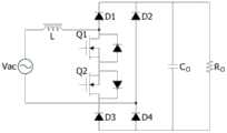
图2至图6属于无桥功因校正转换器(bridgeless PFC)构架,可以降低桥式整流二极管的损耗,但是开机涌浪电流以及高输出电压的缺点无法克服。Figures 2 to 6 belong to the bridgeless PFC architecture, which can reduce the losses of the bridge rectifier diodes, but the shortcomings of the inrush current and high output voltage cannot be overcome.
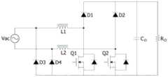
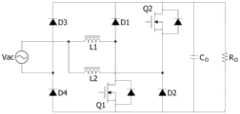
图7与图8属于无桥升降压式交流对直流转换器,可以降低桥式整流的损耗,也能克服开关涌浪电流的问题,同时降低输出电压,惟这样的电路构架产生了元件数量过多、成本过高的问题。Figures 7 and 8 belong to bridgeless buck-boost AC-to-DC converters, which can reduce the loss of bridge rectification, overcome the problem of switching inrush current, and reduce the output voltage at the same time, but such a circuit structure produces a large number of components. Excessive, cost-prohibitive problems.
发明内容SUMMARY OF THE INVENTION
为解决上述现有技术桥式整流损耗、开关涌浪电流、高输出电压、以及元件数量过多、成本过高的问题,本发明提供一种无桥升降压式交流对直流转换器。In order to solve the above-mentioned problems of bridge rectification loss, switching surge current, high output voltage, excessive number of components and high cost in the prior art, the present invention provides a bridgeless buck-boost AC-to-DC converter.
为了达成上述目的所采取的主要技术手段,该无桥升降压式交流对直流转换器包含第一线路、第二线路、第三二极体以及第四二极体。该第一线路具有第一端、第二端以及第三端,该第一端耦接该交流输入电源的第一端,该第二端耦接一接地端,该第三端耦接该直流输出电源的该正极端或该负极端。该第二线路具有第一端、第二端以及第三端,该第一端耦接该交流输入电源的第二端,该第二端耦接该接地端,该第三端耦接该直流输出电源的该正极端或该负极端。该第三二极体耦接该第二线路的该第一端与该接地端之间。该第四二极体耦接该第一线路的该第一端与该接地端之间。In order to achieve the above-mentioned main technical means, the bridgeless buck-boost AC-to-DC converter includes a first line, a second line, a third diode and a fourth diode. The first line has a first end, a second end and a third end, the first end is coupled to the first end of the AC input power supply, the second end is coupled to a ground end, and the third end is coupled to the DC The positive terminal or the negative terminal of the output power supply. The second line has a first end, a second end and a third end, the first end is coupled to the second end of the AC input power supply, the second end is coupled to the ground end, and the third end is coupled to the DC The positive terminal or the negative terminal of the output power supply. The third diode is coupled between the first end of the second line and the ground end. The fourth diode is coupled between the first end of the first line and the ground end.
作为优选,该第一线路包含第一开关、第一电感以及第一二极管。该第一开关具有第一端、第二端以及控制端,其中该第一开关的该第一端耦接该交流输入电源的该第一端。该第一电感具有第一端与第二端,其中该第一电感的该第一端耦接该第一开关的该第二端,该第一电感的该第二端耦接该接地端。该第一二极管具有一阴极端与一阳极端,其中该第一二极管的该阴极端耦接该第一开关的该第二端与该第一电感的该第一端,该第一二极管的该阳极端耦接该直流输出电源的该正极端或该负极端。Preferably, the first circuit includes a first switch, a first inductor and a first diode. The first switch has a first terminal, a second terminal and a control terminal, wherein the first terminal of the first switch is coupled to the first terminal of the AC input power supply. The first inductor has a first terminal and a second terminal, wherein the first terminal of the first inductor is coupled to the second terminal of the first switch, and the second terminal of the first inductor is coupled to the ground terminal. The first diode has a cathode terminal and an anode terminal, wherein the cathode terminal of the first diode is coupled to the second terminal of the first switch and the first terminal of the first inductor. The anode terminal of a diode is coupled to the positive terminal or the negative terminal of the DC output power supply.
作为优选,该第二线路包含第二开关、第二电感以及第二二极体。该第二开关具有第一端、第二端以及控制端,其中该第二开关的该第一端耦接该交流输入电源的该第二端。该第二电感具有第一端与第二端,其中该第二电感的该第一端耦接该第二开关的该第二端,该第二电感的该第二端耦接该接地端。该第二二极体具有一阴极端与阳极端,其中该第二二极体的该阴极端耦接该第二开关的该第二端与该第二电感的该第一端,该第二二极管的该阳极端耦接该直流输出电源的该正极端或该负极端。Preferably, the second circuit includes a second switch, a second inductor and a second diode. The second switch has a first end, a second end and a control end, wherein the first end of the second switch is coupled to the second end of the AC input power supply. The second inductor has a first terminal and a second terminal, wherein the first terminal of the second inductor is coupled to the second terminal of the second switch, and the second terminal of the second inductor is coupled to the ground terminal. The second diode has a cathode end and an anode end, wherein the cathode end of the second diode is coupled to the second end of the second switch and the first end of the second inductor, the second The anode terminal of the diode is coupled to the positive terminal or the negative terminal of the DC output power supply.
作为优选,该第一开关的该控制端接收第一控制信号;当该交流输入电源为正半周且该第一控制信号控制该第一开关导通时,该第一电感进行储能;当该交流输入电源为正半周且该第一控制信号控制该第一开关关断时,该第一电感进行释能。Preferably, the control terminal of the first switch receives a first control signal; when the AC input power is a positive half cycle and the first control signal controls the first switch to be turned on, the first inductor stores energy; When the AC input power is a positive half cycle and the first control signal controls the first switch to be turned off, the first inductor discharges energy.
作为优选,该第一电感通过正半周储能回路进行储能,其中该正半周储能回路是通过该交流输入电源、该第一开关、该第一电感、该第三二极体以及该交流输入电源所形成。Preferably, the first inductor stores energy through a positive half-cycle energy storage circuit, wherein the positive half-cycle energy storage circuit is stored through the AC input power supply, the first switch, the first inductor, the third diode and the AC formed by the input power.
作为优选,该第一电感通过一正半周释能回路进行释能,其中该正半周释能回路是通过该第一电感、耦接该直流输出电源的该正极端与该负极端之间的一负载、该第一二极管以及该第一电感所形成。Preferably, the first inductance discharges energy through a positive half-cycle energy release loop, wherein the positive half-cycle energy release loop is coupled between the positive terminal and the negative terminal of the DC output power through the first inductance The load, the first diode and the first inductor are formed.
作为优选,,该第二开关的该控制端接收一第二控制信号;当该交流输入电源为负半周且该第二控制信号控制该第二开关导通时,该第二电感进行储能;当该交流输入电源为负半周且该第二控制信号控制该第二开关关断时,该第二电感进行释能。Preferably, the control terminal of the second switch receives a second control signal; when the AC input power is in a negative half cycle and the second control signal controls the second switch to be turned on, the second inductor stores energy; When the AC input power is in a negative half cycle and the second control signal controls the second switch to be turned off, the second inductor discharges energy.
作为优选,该第二电感通过一负半周储能回路进行储能,其中该负半周储能回路是通过该交流输入电源、该第二开关、该第二电感、该第四二极体以及该交流输入电源所形成。Preferably, the second inductance stores energy through a negative half-cycle energy storage loop, wherein the negative half-cycle energy storage loop is through the AC input power supply, the second switch, the second inductance, the fourth diode and the formed by AC input power.
作为优选,该第二电感通过一负半周释能回路进行释能,其中该负半周释能回路是通过该第二电感、耦接该直流输出电源的该正极端与该负极端之间的一负载、该第二二极管以及该第二电感所形成。Preferably, the second inductance discharges energy through a negative half-cycle energy release loop, wherein the negative half-cycle energy release loop is coupled between the positive terminal and the negative terminal of the DC output power through the second inductance The load, the second diode and the second inductor are formed.
作为优选,该直流输出电源的该负极端耦接该接地端。Preferably, the negative terminal of the DC output power supply is coupled to the ground terminal.
本发明的有益效果:1、功因校正转换器可以不需要桥式整流电路,进而可提高转换效率;The beneficial effects of the present invention are as follows: 1. The power factor correction converter does not need a bridge rectifier circuit, thereby improving the conversion efficiency;
2、直流输出电源的电压可以高于或低于交流输入电源的电压,因此输出端可选用耐压较低的电容,或亦可使用高耐压功率开关达到高输入涌浪电压的耐受能力;2. The voltage of the DC output power supply can be higher or lower than the voltage of the AC input power supply, so the output terminal can choose a capacitor with a lower withstand voltage, or a high withstand voltage power switch can be used to achieve high input surge voltage tolerance ;
3、无须增加开机的涌浪电流限制器,例如热敏电阻或继电器,如此可避免开机继电器声音,而可作为非网通应用;3. There is no need to add an inrush current limiter, such as a thermistor or a relay, which can avoid the sound of the power-on relay, and can be used as a non-netcom application;
4、可以操作于不连续导通模式、连续导通模式以及临界导通模式。4. Can operate in discontinuous conduction mode, continuous conduction mode and critical conduction mode.
附图说明Description of drawings
为了更清楚地说明本发明实施例或现有技术中的技术方案,下面将对实施例或现有技术描述中所需要使用的附图作简单地介绍,显而易见地,下面描述中的附图仅仅是本发明的一些实施例,对于本领域普通技术人员来讲,在不付出创造性劳动性的前提下,还可以根据这些附图获得其他的附图。In order to explain the embodiments of the present invention or the technical solutions in the prior art more clearly, the following briefly introduces the accompanying drawings that need to be used in the description of the embodiments or the prior art. Obviously, the accompanying drawings in the following description are only These are some embodiments of the present invention, and for those of ordinary skill in the art, other drawings can also be obtained from these drawings without any creative effort.
图1为现有技术的升压型功因校正转换器的电路图;1 is a circuit diagram of a boost-type power factor correction converter in the prior art;
图2为现有技术的无桥功因校正转换器的电路图;2 is a circuit diagram of a bridgeless power factor correction converter in the prior art;
图3为现有技术的无桥功因校正转换器的电路图;3 is a circuit diagram of a prior art bridgeless power factor correction converter;
图4为现有技术的无桥功因校正转换器的电路图;4 is a circuit diagram of a bridgeless power factor correction converter in the prior art;
图5为现有技术的无桥功因校正转换器的电路图;5 is a circuit diagram of a bridgeless power factor correction converter in the prior art;
图6为现有技术的无桥功因校正转换器的电路图;6 is a circuit diagram of a prior art bridgeless power factor correction converter;
图7为现有技术的无桥升降压式交流对直流转换器的电路图;7 is a circuit diagram of a prior art bridgeless buck-boost AC-to-DC converter;
图8为现有技术的无桥升降压式交流对直流转换器的电路图;8 is a circuit diagram of a prior art bridgeless buck-boost AC-to-DC converter;
图9为本发明无桥升降压式交流对直流转换器的电路图;9 is a circuit diagram of a bridgeless buck-boost AC-to-DC converter of the present invention;
图10A为本发明无桥升降压式交流对直流转换器处于一正半周储能操作的电路图;10A is a circuit diagram of a bridgeless buck-boost AC-to-DC converter in a positive half-cycle energy storage operation according to the present invention;
图10B为本发明无桥升降压式交流对直流转换器处于一正半周释能操作的电路图;10B is a circuit diagram of a bridgeless buck-boost AC-to-DC converter in a positive half-cycle energy release operation according to the present invention;
图11A为本发明无桥升降压式交流对直流转换器处于一负半周储能操作的电路图;11A is a circuit diagram of the bridgeless buck-boost AC-to-DC converter of the present invention in a negative half-cycle energy storage operation;
图11B为本发明无桥升降压式交流对直流转换器处于一负半周释能操作的电路图。FIG. 11B is a circuit diagram of the bridgeless buck-boost AC-to-DC converter in a negative half-cycle energy release operation according to the present invention.
图中,Vac:交流输入电源、Vo:直流输出电源、10:第一线路、Q1:第一开关、L1:第一电感、D1:第一二极管、20:第二线路、Q2:第二开关、L2:第二电感、D2:第二二极体、D3:第三二极体、D4:第四二极体、Co:输出电容、Lps:正半周储能回路、Lpr:正半周释能回路、Lns:负半周储能回路、Lnr:负半周释能回路。In the figure, Vac: AC input power, Vo: DC output power, 10: The first line, Q1: The first switch, L1: The first inductor, D1: The first diode, 20: The second line, Q2: The first Two switches, L2: Second inductor, D2: Second diode, D3: Third diode, D4: Fourth diode, Co: Output capacitor, Lps: Positive half cycle energy storage circuit, Lpr: Positive half cycle Energy release circuit, Lns: negative half cycle energy storage circuit, Lnr: negative half cycle energy release circuit.
具体实施方式Detailed ways
为使本发明的目的、技术方案和优点更加清楚明了,下面结合具体实施方式并参照附图,对本发明进一步详细说明。应该理解,这些描述只是示例性的,而并非要限制本发明的范围。此外,在以下说明中,省略了对公知结构和技术的描述,以避免不必要地混淆本发明的概念。In order to make the objectives, technical solutions and advantages of the present invention clearer, the present invention will be further described in detail below with reference to the specific embodiments and the accompanying drawings. It should be understood that these descriptions are exemplary only and are not intended to limit the scope of the invention. Also, in the following description, descriptions of well-known structures and techniques are omitted to avoid unnecessarily obscuring the concepts of the present invention.
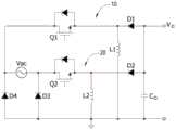
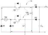
具体实施例一:请参见图9所示,该无桥升降压式交流对直流转换器用以转换交流输入电源Vac,进而在输出电容Co上提供具有正极端与负极端的直流输出电源Vo。该无桥升降压式交流对直流转换器包含第一线路10、第二线路20、第三二极体D3以及第四二极体D4。Embodiment 1: Referring to FIG. 9 , the bridgeless buck-boost AC-to-DC converter is used to convert the AC input power Vac, and then provide a DC output power Vo with a positive terminal and a negative terminal on the output capacitor Co. The bridgeless buck-boost AC-to-DC converter includes a
该第一线路10具有第一端、第二端以及第三端。该第一端耦接该交流输入电源Vac的第一端,该第二端耦接接地端,该第三端耦接该直流输出电源Vo的该正极端或该负极端。该第二线路20具有第一端、第二端以及第三端,该第一端耦接该交流输入电源Vac的第二端,该第二端耦接该接地端,该第三端耦接该直流输出电源Vo的该正极端或该负极端。该第三二极体D3耦接该第二线路20的该第一端与该接地端之间。该第四二极体D4耦接该第一线路10的该第一端与该接地端之间。其中,该直流输出电源Vo的该负极端耦接该接地端。The
具体地,该第一线路10包含第一开关Q1、第一电感L1以及第一二极管D1。该第一开关Q1具有一第一端、第二端以及一控制端,例如为三端的功率开关元件。其中该第一开关Q1的该第一端耦接该交流输入电源Vac的该第一端。该第一电感L1具有第一端与第二端,其中该第一电感L1的该第一端耦接该第一开关Q1的该第二端,该第一电感L1的该第二端耦接该接地端。该第一二极管D1具有阴极端与一阳极端,其中该第一二极管D1的该阴极端耦接该第一开关Q1的该第二端与该第一电感L1的该第一端,该第一二极管D1的该阳极端耦接该直流输出电源Vo的该正极端或该负极端。Specifically, the
具体地,该第二线路20包含第二开关Q2、第二电感L2以及第二二极体D2。该第二开关Q2具有第一端、第二端以及控制端,例如为三端的功率开关元件。其中该第二开关Q2的该第一端耦接该交流输入电源Vac的该第二端。该第二电感L2具有第一端与第二端,其中该第二电感L2的该第一端耦接该第二开关Q2的该第二端,该第二电感L2的该第二端耦接该接地端。该第二二极体D2具有阴极端与阳极端,其中该第二二极体D2的该阴极端耦接该第二开关Q2的该第二端与该第二电感L2的该第一端,该第二二极体D2的该阳极端耦接该直流输出电源Vo的该正极端或该负极端。Specifically, the
请参见图10A与图10B所示,其分别为本发明无桥升降压式交流对直流转换器处于正半周储能操作与正半周释能操作的电路图。该第一开关Q1的该控制端接收第一控制信号。当该交流输入电源Vac为正半周且该第一控制信号控制该第一开关Q1导通时,该第一电感L1进行储能。当该交流输入电源Vac为正半周且该第一控制信号控制该第一开关Q1关断时,该第一电感L1进行释能。Please refer to FIG. 10A and FIG. 10B , which are circuit diagrams of the bridgeless buck-boost AC-to-DC converter in the positive half cycle energy storage operation and the positive half cycle energy release operation, respectively. The control terminal of the first switch Q1 receives a first control signal. When the AC input power Vac is in a positive half cycle and the first control signal controls the first switch Q1 to be turned on, the first inductor L1 stores energy. When the AC input power Vac is in a positive half cycle and the first control signal controls the first switch Q1 to turn off, the first inductor L1 discharges energy.
如图10A所示,该第一电感L1通过正半周储能回路Lps进行储能,其中该正半周储能回路Lps是通过该交流输入电源Vac、该第一开关Q1、该第一电感L1、该第三二极体D3以及该交流输入电源Vac所形成。在此操作下,该第二开关Q2可为导通状态,也可为关断状态。As shown in FIG. 10A , the first inductor L1 stores energy through a positive half-cycle energy storage circuit Lps, wherein the positive half-cycle energy storage circuit Lps is stored through the AC input power supply Vac, the first switch Q1, the first inductor L1, The third diode D3 and the AC input power Vac are formed. Under this operation, the second switch Q2 can be in an on state or in an off state.
如图10B所示,该第一电感L1通过正半周释能回路Lpr进行释能,其中该正半周释能回路Lpr是通过该第一电感L1、耦接该直流输出电源Vo的该正极端与该负极端之间的一负载(图未示)、该第一二极体D1以及该第一电感L1所形成。As shown in FIG. 10B , the first inductor L1 discharges energy through a positive half-cycle energy release loop Lpr, wherein the positive half-cycle energy release loop Lpr is coupled to the positive terminal of the DC output power Vo and the first inductor L1 through the first inductor L1. A load (not shown) between the negative terminals, the first diode D1 and the first inductor L1 are formed.
请参见图11A与图11B所示,其分别为本发明无桥升降压式交流对直流转换器处于负半周储能操作与负半周释能操作的电路图。该第二开关Q2的该控制端接收第二控制信号。当该交流输入电源Vac为负半周且该第二控制信号控制该第二开关Q2导通时,该第二电感L2进行储能。当该交流输入电源Vac为负半周且该第二控制信号控制该第二开关Q2关断时,该第二电感L2进行释能。Please refer to FIG. 11A and FIG. 11B , which are circuit diagrams of the bridgeless buck-boost AC-to-DC converter in the negative half cycle energy storage operation and the negative half cycle energy release operation, respectively. The control terminal of the second switch Q2 receives a second control signal. When the AC input power Vac is in a negative half cycle and the second control signal controls the second switch Q2 to be turned on, the second inductor L2 stores energy. When the AC input power Vac is in a negative half cycle and the second control signal controls the second switch Q2 to turn off, the second inductor L2 discharges energy.
如图11A所示,该第二电感L2通过负半周储能回路Lns进行储能,其中该负半周储能回路Lns是通过该交流输入电源Vac、该第二开关Q2、该第二电感L2、该第四二极体D4以及该交流输入电源Vac所形成。在此操作下,该第一开关Q1可为导通状态,也可为关断状态。As shown in FIG. 11A , the second inductor L2 stores energy through a negative half-cycle energy storage circuit Lns, wherein the negative half-cycle energy storage circuit Lns is stored through the AC input power supply Vac, the second switch Q2, the second inductor L2, The fourth diode D4 and the AC input power Vac are formed. Under this operation, the first switch Q1 can be in an on state or in an off state.
如图11B所示,该第二电感L2通过一负半周释能回路Lnr进行释能,其中该负半周释能回路Lnr是通过该第二电感L2、耦接该直流输出电源Vo的该正极端与该负极端之间的负载(图未示)、该第二二极体D2以及该第二电感L2所形成。As shown in FIG. 11B , the second inductor L2 discharges energy through a negative half-cycle energy release loop Lnr, wherein the negative half-cycle energy release loop Lnr is coupled to the positive terminal of the DC output power Vo through the second inductor L2 The load (not shown) between the negative terminal, the second diode D2 and the second inductor L2 is formed.
以上所述,仅为本发明较佳具体实施例之详细说明与图式,惟本发明之特征并不局限于此,并非用以限制本发明,本发明之所有范围应以下述之申请专利范围为准,凡合于本发明申请专利范围之精神与其类似变化之实施例,皆应包含于本发明之范畴中,任何熟悉该项技艺者在本发明之领域内,可轻易思及之变化或修饰皆可涵盖在以下本案之专利范围。The above descriptions are only detailed descriptions and drawings of the preferred embodiments of the present invention, but the features of the present invention are not limited thereto, and are not intended to limit the present invention. The entire scope of the present invention should be defined as the following claims All the embodiments that conform to the spirit of the scope of the patent application of the present invention and similar variations thereof shall be included in the scope of the present invention. Modifications can be covered by the following patent scope of this case.
Claims (10)
Priority Applications (1)
| Application Number | Priority Date | Filing Date | Title |
|---|---|---|---|
| CN202010346605.1ACN111416532B (en) | 2020-04-27 | 2020-04-27 | A bridgeless buck-boost AC-to-DC converter |
Applications Claiming Priority (1)
| Application Number | Priority Date | Filing Date | Title |
|---|---|---|---|
| CN202010346605.1ACN111416532B (en) | 2020-04-27 | 2020-04-27 | A bridgeless buck-boost AC-to-DC converter |
Publications (2)
| Publication Number | Publication Date |
|---|---|
| CN111416532Atrue CN111416532A (en) | 2020-07-14 |
| CN111416532B CN111416532B (en) | 2022-11-08 |
Family
ID=71494949
Family Applications (1)
| Application Number | Title | Priority Date | Filing Date |
|---|---|---|---|
| CN202010346605.1AActiveCN111416532B (en) | 2020-04-27 | 2020-04-27 | A bridgeless buck-boost AC-to-DC converter |
Country Status (1)
| Country | Link |
|---|---|
| CN (1) | CN111416532B (en) |
Cited By (7)
| Publication number | Priority date | Publication date | Assignee | Title |
|---|---|---|---|---|
| CN113037074A (en)* | 2021-02-26 | 2021-06-25 | 广州金升阳科技有限公司 | Bridgeless voltage reduction power factor correction circuit |
| CN113224942A (en)* | 2021-06-16 | 2021-08-06 | 广东工业大学 | Non-isolated Buck-Boost bridgeless PFC converter system |
| CN114204803A (en)* | 2020-08-28 | 2022-03-18 | 中山旭贵明电子有限公司 | Power supply conversion circuit and current converter for split-phase power supply system |
| CN114900057A (en)* | 2022-04-29 | 2022-08-12 | 湖南珂拓电子科技有限公司 | High Efficiency Buck-Boost Rectifier Topology and Control Method |
| CN116365900A (en)* | 2023-03-01 | 2023-06-30 | 西南交通大学 | AC input asymmetric bridgeless buck PFC converter |
| CN117060710A (en)* | 2023-08-21 | 2023-11-14 | 哈尔滨工业大学 | Single-phase bridgeless buck-boost PFC converter |
| CN118826512A (en)* | 2024-08-30 | 2024-10-22 | 西南交通大学 | High-efficiency bridgeless boost rectifier circuit for low-voltage energy recovery sources |
Citations (7)
| Publication number | Priority date | Publication date | Assignee | Title |
|---|---|---|---|---|
| TW200938988A (en)* | 2008-03-11 | 2009-09-16 | Delta Electronics Inc | Bridgeless PFC for critical conduction mode and controlling method thereof |
| CN101931319A (en)* | 2009-06-08 | 2010-12-29 | 康舒科技股份有限公司 | Bridgeless Power Factor Correction Circuit |
| CN104218825A (en)* | 2013-05-30 | 2014-12-17 | 弗莱克斯电子有限责任公司 | Bridgeless pfc power converter with high efficiency |
| CN104300810A (en)* | 2013-07-17 | 2015-01-21 | 台达电子企业管理(上海)有限公司 | Power factor correction converter and control method |
| CN107204717A (en)* | 2017-06-07 | 2017-09-26 | 福州大学 | A kind of Bridgeless boost type CUK pfc circuits |
| CN109104087A (en)* | 2018-11-08 | 2018-12-28 | 亚瑞源科技(深圳)有限公司 | A kind of DC-DC converter with no bridge type power factor debugging functions |
| CN110299832A (en)* | 2018-03-21 | 2019-10-01 | 群光电能科技股份有限公司 | Without bridge alternating expression power factor corrector and its control method |
- 2020
- 2020-04-27CNCN202010346605.1Apatent/CN111416532B/enactiveActive
Patent Citations (7)
| Publication number | Priority date | Publication date | Assignee | Title |
|---|---|---|---|---|
| TW200938988A (en)* | 2008-03-11 | 2009-09-16 | Delta Electronics Inc | Bridgeless PFC for critical conduction mode and controlling method thereof |
| CN101931319A (en)* | 2009-06-08 | 2010-12-29 | 康舒科技股份有限公司 | Bridgeless Power Factor Correction Circuit |
| CN104218825A (en)* | 2013-05-30 | 2014-12-17 | 弗莱克斯电子有限责任公司 | Bridgeless pfc power converter with high efficiency |
| CN104300810A (en)* | 2013-07-17 | 2015-01-21 | 台达电子企业管理(上海)有限公司 | Power factor correction converter and control method |
| CN107204717A (en)* | 2017-06-07 | 2017-09-26 | 福州大学 | A kind of Bridgeless boost type CUK pfc circuits |
| CN110299832A (en)* | 2018-03-21 | 2019-10-01 | 群光电能科技股份有限公司 | Without bridge alternating expression power factor corrector and its control method |
| CN109104087A (en)* | 2018-11-08 | 2018-12-28 | 亚瑞源科技(深圳)有限公司 | A kind of DC-DC converter with no bridge type power factor debugging functions |
Cited By (11)
| Publication number | Priority date | Publication date | Assignee | Title |
|---|---|---|---|---|
| CN114204803A (en)* | 2020-08-28 | 2022-03-18 | 中山旭贵明电子有限公司 | Power supply conversion circuit and current converter for split-phase power supply system |
| CN114204803B (en)* | 2020-08-28 | 2023-09-22 | 中山旭贵明电子有限公司 | Power supply conversion circuit and converter for split-phase power supply system |
| CN113037074A (en)* | 2021-02-26 | 2021-06-25 | 广州金升阳科技有限公司 | Bridgeless voltage reduction power factor correction circuit |
| WO2022179564A1 (en)* | 2021-02-26 | 2022-09-01 | 广州金升阳科技有限公司 | Bridgeless voltage-drop power factor correction circuit |
| CN113224942A (en)* | 2021-06-16 | 2021-08-06 | 广东工业大学 | Non-isolated Buck-Boost bridgeless PFC converter system |
| CN113224942B (en)* | 2021-06-16 | 2022-04-15 | 广东工业大学 | Non-isolated Buck-Boost bridgeless PFC converter system |
| CN114900057A (en)* | 2022-04-29 | 2022-08-12 | 湖南珂拓电子科技有限公司 | High Efficiency Buck-Boost Rectifier Topology and Control Method |
| CN116365900A (en)* | 2023-03-01 | 2023-06-30 | 西南交通大学 | AC input asymmetric bridgeless buck PFC converter |
| CN116365900B (en)* | 2023-03-01 | 2023-11-03 | 西南交通大学 | AC input asymmetric bridgeless buck PFC converter |
| CN117060710A (en)* | 2023-08-21 | 2023-11-14 | 哈尔滨工业大学 | Single-phase bridgeless buck-boost PFC converter |
| CN118826512A (en)* | 2024-08-30 | 2024-10-22 | 西南交通大学 | High-efficiency bridgeless boost rectifier circuit for low-voltage energy recovery sources |
Also Published As
| Publication number | Publication date |
|---|---|
| CN111416532B (en) | 2022-11-08 |
Similar Documents
| Publication | Publication Date | Title |
|---|---|---|
| CN111416532B (en) | A bridgeless buck-boost AC-to-DC converter | |
| US11223275B2 (en) | Switching mode power supply circuit | |
| US8098500B2 (en) | Phase shift full bridge converter with reduced current stress | |
| US8736238B2 (en) | Buck and buck/boost converter systems having auxiliary circuits and method thereof | |
| CN103401466B (en) | Inverter system | |
| US11128220B2 (en) | Switching mode power supply circuit for three phase AC input | |
| TWI737177B (en) | Bridgeless step-up and step-down ac-to-dc converter | |
| Pandey et al. | Canonical switching cell (CSC) converter-based power factor-corrected battery charger for e-rickshaw | |
| WO2020052617A1 (en) | Bridgeless triple-rectifier boost power supply circuit | |
| CN110165921A (en) | One kind having the quasi- Z-source inverter of high output voltage gain switch inductive type | |
| CN115580121A (en) | Lightning protected power supply | |
| TWI320989B (en) | ||
| CN100514807C (en) | EMI-reducing single-stage power factor correcting circuit | |
| TWI658678B (en) | Uninterruptible power supply apparatus | |
| CN104779784A (en) | Single-phase power factor corrector with voltage boosting and reduction functions | |
| US20220311331A1 (en) | Adaptive energy storage circuit | |
| CN103683895B (en) | Bridgeless power factor corrector with single inductive element and method of operation thereof | |
| CN111525783A (en) | Converter and switch mode power supply | |
| CN112689363A (en) | Power converter | |
| TW201806297A (en) | Power factor correction circuit and corrector thereof | |
| Hsu et al. | A single stage single switch valley switching Flyback-Forward converter with regenerative snubber and PFC for LED light source system | |
| CN109962474A (en) | Uninterruptible power supply device | |
| CN212033991U (en) | Three-phase LC series current-limiting circuit | |
| CN206620063U (en) | Single-phase optocoupler times flow pattern buck rectifier | |
| TW201411309A (en) | Bridgeless power factor corrector with single choke and method of operating the same |
Legal Events
| Date | Code | Title | Description |
|---|---|---|---|
| PB01 | Publication | ||
| PB01 | Publication | ||
| SE01 | Entry into force of request for substantive examination | ||
| SE01 | Entry into force of request for substantive examination | ||
| GR01 | Patent grant | ||
| GR01 | Patent grant |