CN111403463B - Touch display panel, manufacturing method thereof and display device - Google Patents
Touch display panel, manufacturing method thereof and display deviceDownload PDFInfo
- Publication number
- CN111403463B CN111403463BCN202010234947.4ACN202010234947ACN111403463BCN 111403463 BCN111403463 BCN 111403463BCN 202010234947 ACN202010234947 ACN 202010234947ACN 111403463 BCN111403463 BCN 111403463B
- Authority
- CN
- China
- Prior art keywords
- layer
- touch
- overlapping
- base substrate
- display panel
- Prior art date
- Legal status (The legal status is an assumption and is not a legal conclusion. Google has not performed a legal analysis and makes no representation as to the accuracy of the status listed.)
- Active
Links
Images


Classifications
- H—ELECTRICITY
- H10—SEMICONDUCTOR DEVICES; ELECTRIC SOLID-STATE DEVICES NOT OTHERWISE PROVIDED FOR
- H10K—ORGANIC ELECTRIC SOLID-STATE DEVICES
- H10K59/00—Integrated devices, or assemblies of multiple devices, comprising at least one organic light-emitting element covered by group H10K50/00
- H10K59/40—OLEDs integrated with touch screens
- G—PHYSICS
- G06—COMPUTING OR CALCULATING; COUNTING
- G06F—ELECTRIC DIGITAL DATA PROCESSING
- G06F3/00—Input arrangements for transferring data to be processed into a form capable of being handled by the computer; Output arrangements for transferring data from processing unit to output unit, e.g. interface arrangements
- G06F3/01—Input arrangements or combined input and output arrangements for interaction between user and computer
- G06F3/03—Arrangements for converting the position or the displacement of a member into a coded form
- G06F3/041—Digitisers, e.g. for touch screens or touch pads, characterised by the transducing means
- G06F3/0412—Digitisers structurally integrated in a display
- H—ELECTRICITY
- H10—SEMICONDUCTOR DEVICES; ELECTRIC SOLID-STATE DEVICES NOT OTHERWISE PROVIDED FOR
- H10K—ORGANIC ELECTRIC SOLID-STATE DEVICES
- H10K59/00—Integrated devices, or assemblies of multiple devices, comprising at least one organic light-emitting element covered by group H10K50/00
- H10K59/10—OLED displays
- H—ELECTRICITY
- H10—SEMICONDUCTOR DEVICES; ELECTRIC SOLID-STATE DEVICES NOT OTHERWISE PROVIDED FOR
- H10K—ORGANIC ELECTRIC SOLID-STATE DEVICES
- H10K71/00—Manufacture or treatment specially adapted for the organic devices covered by this subclass
Landscapes
- Engineering & Computer Science (AREA)
- General Engineering & Computer Science (AREA)
- Theoretical Computer Science (AREA)
- Human Computer Interaction (AREA)
- Physics & Mathematics (AREA)
- General Physics & Mathematics (AREA)
- Manufacturing & Machinery (AREA)
- Electroluminescent Light Sources (AREA)
- Devices For Indicating Variable Information By Combining Individual Elements (AREA)
Abstract
Translated fromChinese
Description
Translated fromChinese技术领域technical field
本申请涉及显示技术领域,具体而言,涉及一种触控显示面板及其制备方法、显示装置。The present application relates to the field of display technology, in particular, to a touch display panel, a manufacturing method thereof, and a display device.
背景技术Background technique
屏内触控(Incell Touch)技术在显示领域是一种极具优势的解决方案,其以窄边框、低成本、高触摸性能、更轻薄等优势一直是技术开发的热点。In-screen touch (Incell Touch) technology is a very advantageous solution in the display field. It has always been a hot spot in technology development due to its advantages such as narrow frame, low cost, high touch performance, and thinner.
在OLED显示领域,特别是OLED穿戴显示设备中,将触控结构内嵌于OLED面板中,可以节省玻璃成本和贴合成本,使得面板重量轻、透光度高,更满足显示面板对品质的要求。但由于屏内膜层结构变得复杂,保证触控结构能够与触控信号线稳定接触是保证良好触控效果的关键问题。In the field of OLED display, especially in OLED wearable display devices, embedding the touch structure in the OLED panel can save glass cost and bonding cost, make the panel light in weight and high in light transmittance, and better meet the quality requirements of the display panel. Require. However, due to the complexity of the film layer structure in the screen, ensuring that the touch structure can be in stable contact with the touch signal line is the key issue to ensure a good touch effect.
需要说明的是,在上述背景技术部分发明的信息仅用于加强对本申请的背景的理解,因此可以包括不构成对本领域普通技术人员已知的现有技术的信息。It should be noted that the information disclosed in the above background technology section is only used to enhance the understanding of the background of the application, and therefore may include information that does not constitute prior art known to those of ordinary skill in the art.
发明内容Contents of the invention
本申请的目的在于提供一种触控显示面板及其制备方法、显示装置,解决现有技术存在的一种或多种问题。The purpose of the present application is to provide a touch display panel, a manufacturing method thereof, and a display device, so as to solve one or more problems existing in the prior art.
根据本申请的一个方面,提供一种触控显示面板,包括:According to one aspect of the present application, a touch display panel is provided, including:
相对设置的衬底基板和封装盖板,所述衬底基板和封装盖板均包括显示区和围绕所述显示区设置的周边区;A base substrate and a packaging cover plate that are oppositely arranged, and each of the base substrate and the packaging cover plate includes a display area and a peripheral area arranged around the display area;
触控电极层,设于所述封装盖板的显示区;The touch electrode layer is arranged in the display area of the package cover;
第一搭接层,设于所述封装盖板的周边区,连接所述触控电极层,且所述第一搭接层的材料为导电材料;The first bonding layer is arranged in the peripheral area of the packaging cover and connected to the touch electrode layer, and the material of the first bonding layer is a conductive material;
支撑层,设于所述衬底基板的周边区;a supporting layer disposed on the peripheral area of the base substrate;
第二搭接层,设于所述衬底基板的周边区且覆盖所述支撑层,所述第二搭接层的材料为导电材料,所述第二搭接层与所述第一搭接层接触;The second overlapping layer is arranged on the peripheral area of the base substrate and covers the supporting layer, the material of the second overlapping layer is a conductive material, and the second overlapping layer is connected to the first overlapping layer. layer contact;
触控信号线,设于所述衬底基板的周边区,与所述第二搭接层电连接。The touch signal line is arranged in the peripheral area of the base substrate and is electrically connected with the second bonding layer.
在本申请的一种示例性实施例中,所述触控电极层包括相互绝缘的第一触控电极层和第二触控电极层,所述第一搭接层包括多个第一电极,所述第二触控电极层包括多个第二电极,所述第一搭接层包括多个第一搭接部,多个所述第一搭接部与各所述第一电极、各所述第二电极一一对应的电连接,所述第二搭接层包括多个第二搭接部,各所述第二搭接部与各所述第一搭接部一一对应接触。In an exemplary embodiment of the present application, the touch electrode layer includes a first touch electrode layer and a second touch electrode layer that are insulated from each other, the first overlapping layer includes a plurality of first electrodes, The second touch electrode layer includes a plurality of second electrodes, the first bonding layer includes a plurality of first bonding parts, and the multiple first bonding parts are connected to each of the first electrodes and each of the first bonding parts. The second electrodes are electrically connected in one-to-one correspondence, the second overlapping layer includes a plurality of second overlapping portions, and each of the second overlapping portions is in one-to-one contact with each of the first overlapping portions.
在本申请的一种示例性实施例中,所述支撑层包括多个支撑部,所述多个支撑部与各所述第二搭接部一一对应设置。In an exemplary embodiment of the present application, the support layer includes a plurality of support portions, and the plurality of support portions are provided in one-to-one correspondence with each of the second overlapping portions.
在本申请的一种示例性实施例中,所述第一触控电极层和第二触控电极层同层设置或不同层设置。In an exemplary embodiment of the present application, the first touch electrode layer and the second touch electrode layer are arranged in the same layer or in different layers.
在本申请的一种示例性实施例中,各所述第二搭接部均包括依次层叠设置的第一透明导电氧化物层和第一金属层,所述第一金属层与对应的所述第一搭接部接触。In an exemplary embodiment of the present application, each of the second overlapping parts includes a first transparent conductive oxide layer and a first metal layer stacked in sequence, and the first metal layer and the corresponding The first laps are in contact.
在本申请的一种示例性实施例中,所述触控显示面板还包括设于所述衬底基板显示区的发光器件,所述发光器件包括阳极层,所述阳极层包括依次层叠设置的第二透明导电氧化物层、第二金属层和第三透明导电氧化物层;其中,所述第一透明导电氧化物层与所述第二透明导电氧化物层同层设置,所述第一金属层和第二金属层同层设置。In an exemplary embodiment of the present application, the touch display panel further includes a light-emitting device disposed in the display area of the base substrate, the light-emitting device includes an anode layer, and the anode layer includes sequentially stacked The second transparent conductive oxide layer, the second metal layer and the third transparent conductive oxide layer; wherein, the first transparent conductive oxide layer and the second transparent conductive oxide layer are arranged in the same layer, and the first transparent conductive oxide layer The metal layer and the second metal layer are arranged on the same layer.
在本申请的一种示例性实施例中,所述第一透明导电氧化物层的材料为透明氧化铟锡,所述第一金属层的材料为Ag。In an exemplary embodiment of the present application, the material of the first transparent conductive oxide layer is transparent indium tin oxide, and the material of the first metal layer is Ag.
根据本申请的另一个方面,提供一种触控显示面板的制备方法,包括:According to another aspect of the present application, a method for manufacturing a touch display panel is provided, including:
提供一衬底基板和封装盖板,所述衬底基板和封装盖板均包括显示区和围绕所述显示区设置的周边区;A base substrate and a package cover are provided, each of which includes a display area and a peripheral area disposed around the display area;
在所述封装盖板的显示区形成触控电极层,采用导电材料在所述封装盖板的周边区形成第一搭接层,所述第一搭接层连接所述触控电极层;A touch electrode layer is formed in the display area of the package cover, and a first overlapping layer is formed in the peripheral area of the package cover by using a conductive material, and the first overlap layer is connected to the touch electrode layer;
在所述衬底基板的周边区形成支撑层和触控信号线;forming a supporting layer and a touch signal line in the peripheral area of the base substrate;
采用导电材料在所述衬底基板的周边区形成覆盖所述支撑层的第二搭接层,且使所述触控信号线与所述第二搭接层电连接;forming a second bonding layer covering the support layer in the peripheral region of the base substrate by using a conductive material, and electrically connecting the touch signal line to the second bonding layer;
将所述衬底基板和封装盖板对盒,使所述第二搭接层与所述触控电极层接触。The base substrate and the packaging cover plate are boxed together, so that the second bonding layer is in contact with the touch electrode layer.
在本申请的一种示例性实施例中,所述制备方法还包括,在所述衬底基板显示区形成发光器件,所述发光器件包括阳极层,其中,形成所述阳极层和所述第二搭接层包括:In an exemplary embodiment of the present application, the preparation method further includes forming a light emitting device in the display area of the base substrate, the light emitting device includes an anode layer, wherein the anode layer and the second The second lap layer includes:
在所述衬底基板上通过同步构图工艺形成位于所述显示区的第二透明导电氧化物层和位于所述周边区的第一透明导电氧化物层;forming a second transparent conductive oxide layer located in the display area and a first transparent conductive oxide layer located in the peripheral area on the base substrate through a simultaneous patterning process;
通过同步构图工艺形成位于所述显示区的第二金属层和位于所述周边区的第一金属层;forming a second metal layer located in the display area and a first metal layer located in the peripheral area through a simultaneous patterning process;
通过同步构图工艺形成位于所述显示区的第四透明导电氧化物层和位于所述周边区的第三透明导电氧化物层;forming a fourth transparent conductive oxide layer located in the display area and a third transparent conductive oxide layer located in the peripheral area through a simultaneous patterning process;
采用光刻工艺去除所述第三透明导电氧化物层;removing the third transparent conductive oxide layer by photolithography;
对所述第一金属层进行加热,使所述第一金属层生长并能与所述触控电极层接触。The first metal layer is heated so that the first metal layer grows and can be in contact with the touch electrode layer.
根据本申请的第三个方面,提供一种显示装置,包括上述任意一项所述的触控显示面板。According to a third aspect of the present application, a display device is provided, including the touch display panel described in any one of the above.
本申请的触控显示面板中在在封装盖板上设置第一搭接层,衬底基板上对应位置设置第二搭接层,并通过支撑层顶起,使第一搭接层和第二搭接层直接接触,从而将触控电极层产生的信号传递至触控信号线。该结构的第一搭接层能与第二搭接层保持稳定的接触,避免接触不良,确保触控信号的稳定传递,进而可以保证触控面板的良好品质。In the touch display panel of the present application, the first overlapping layer is arranged on the package cover, and the second overlapping layer is arranged at the corresponding position on the base substrate, and is lifted by the supporting layer, so that the first overlapping layer and the second The overlapping layer is in direct contact, so as to transmit the signal generated by the touch electrode layer to the touch signal line. The first overlapping layer of this structure can maintain stable contact with the second overlapping layer, avoid poor contact, ensure stable transmission of touch signals, and thus ensure good quality of the touch panel.
应当理解的是,以上的一般描述和后文的细节描述仅是示例性和解释性的,并不能限制本申请。It is to be understood that both the foregoing general description and the following detailed description are exemplary and explanatory only and are not restrictive of the application.
附图说明Description of drawings
此处的附图被并入说明书中并构成本说明书的一部分,示出了符合本申请的实施例,并与说明书一起用于解释本申请的原理。显而易见地,下面描述中的附图仅仅是本申请的一些实施例,对于本领域普通技术人员来讲,在不付出创造性劳动的前提下,还可以根据这些附图获得其他的附图。The accompanying drawings, which are incorporated in and constitute a part of this specification, illustrate embodiments consistent with the application and together with the description serve to explain the principles of the application. Apparently, the drawings in the following description are only some embodiments of the present application, and those skilled in the art can obtain other drawings according to these drawings without creative efforts.
图1为本实施方式衬底基板的俯视结构示意图;FIG. 1 is a schematic top view of a substrate substrate in this embodiment;
图2为本实施方式封装基板的仰视结构示意图;FIG. 2 is a schematic bottom view of the package substrate in this embodiment;
图3为本实施方式对自电容式触控显示面板的结构示意图;FIG. 3 is a schematic structural diagram of a self-capacitive touch display panel in this embodiment;
图4为本实施方式为互电容式触控显示面板的一种结构示意图;FIG. 4 is a schematic structural diagram of a mutual capacitive touch display panel in this embodiment;
图5为本实施方式为互电容式触控显示面板的另一种结构示意图;FIG. 5 is a schematic diagram of another structure of a mutual capacitive touch display panel in this embodiment;
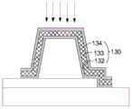
图6为本实施方式中一种第二搭接层的结构示意图;FIG. 6 is a schematic structural view of a second overlapping layer in this embodiment;
图7为本实施方式中触控显示面板的制备方法流程图;FIG. 7 is a flowchart of a method for manufacturing a touch display panel in this embodiment;
图8为本实施方式中掩膜板的结构示意图;FIG. 8 is a schematic structural diagram of a mask plate in this embodiment;
图9为本实施方式中对第二搭接层进行光刻工艺的示意图;FIG. 9 is a schematic diagram of performing a photolithography process on the second bonding layer in this embodiment;
图10为本实施方式中剥离上层ITO后的第二搭接层的示意图;10 is a schematic diagram of the second overlapping layer after peeling off the upper layer ITO in this embodiment;
图11为第一搭接层分别为三层和双层时接触效果的扫描电镜图;Fig. 11 is the scanning electron micrograph of the contact effect when the first overlapping layer is respectively three-layer and double-layer;
图12为第一搭接层分别为三层和双层时金属Ag的透射电镜图。Fig. 12 is a transmission electron microscope image of metal Ag when the first overlapping layer is three layers and two layers respectively.
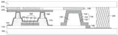
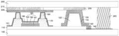
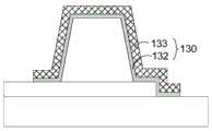
图中:100、衬底基板;110、平坦层;120、支撑层;130、第二搭接层;131、第二搭接部;140、触控信号线;150、引线;160、阳极;170、像素界定层;180、隔垫物;190、发光层;101、阴极;132、第一透明导电氧化物层;133、第一金属层;134、第三透明导电氧化物层;161、第二透明导电氧化物层;162、第二金属层;163、第四透明导电氧化物层;In the figure: 100, base substrate; 110, flat layer; 120, support layer; 130, second overlapping layer; 131, second overlapping portion; 140, touch signal line; 150, lead wire; 160, anode; 170. Pixel defining layer; 180. Spacer; 190. Light emitting layer; 101. Cathode; 132. First transparent conductive oxide layer; 133. First metal layer; 134. Third transparent conductive oxide layer; 161. The second transparent conductive oxide layer; 162, the second metal layer; 163, the fourth transparent conductive oxide layer;
200、封装盖板;210、触控电极层、211、第一触控电极层;212、第二触控电极层;220、绝缘层;230、第一搭接层;231、第一搭接部;240、封装胶。200, package cover plate; 210, touch electrode layer, 211, first touch electrode layer; 212, second touch electrode layer; 220, insulating layer; 230, first overlapping layer; 231, first overlapping Department; 240, packaging glue.
300、掩膜板。300. Mask plate.
具体实施方式Detailed ways
现在将参考附图更全面地描述示例实施方式。然而,示例实施方式能够以多种形式实施,且不应被理解为限于在此阐述的实施方式;相反,提供这些实施方式使得本申请将全面和完整,并将示例实施方式的构思全面地传达给本领域的技术人员。图中相同的附图标记表示相同或类似的结构,因而将省略它们的详细描述。Example embodiments will now be described more fully with reference to the accompanying drawings. Example embodiments may, however, be embodied in many forms and should not be construed as limited to the embodiments set forth herein; rather, these embodiments are provided so that this application will be thorough and complete, and will fully convey the concept of example embodiments to those skilled in the art. The same reference numerals in the drawings denote the same or similar structures, and thus their detailed descriptions will be omitted.
本申请实施方式中提供了一种触控显示面板,应用于OLED显示面板中。参考图1-图3,本申请实施方式的触控显示面板包括对盒设置的衬底基板100和封装盖板200,衬底基板100和封装盖板200均包括显示区和围绕显示区设置的周边区;衬底基板100的显示区设置有发光器件;封装盖板200的显示区设置有触控电极层210,周边区设置有第一搭接层230,第一搭接层230电连接触控电极层210,且第二搭接层130的材料为导电材料;衬底基板100的周边区设置有支撑层120,支撑层120上覆盖有导电的第二搭接层130,第二搭接层130与第一搭接层230接触;衬底基板100的周边区还设置有触控信号线140,触控信号线140与第二搭接层130电连接。Embodiments of the present application provide a touch display panel, which is applied to an OLED display panel. Referring to FIG. 1-FIG. 3, the touch display panel according to the embodiment of the present application includes a
本实施方式中,触控电极层210和第一搭接层230设置在封装盖板200上,触控信号线140和第二搭接层130均设置在衬底基板100上,第一搭接层230和第二搭接层130均为导电材料且二者直接接触,使触控电极层210产生的信号可以传递至触控信号线140。为了实现第一搭接层230和第二搭接层130的接触,在衬底基板100上设置支撑层120,利用支撑层120将第二搭接层130顶起,可以使第一搭接层230始终与第二搭接层130保持稳定的搭接,防止接触不良,确保触控信号的稳定传递,进而保证触控面板的良好品质。In this embodiment, the
下面对本申请实施方式的触控显示面板进行详细说明:The touch display panel in the implementation manner of the present application will be described in detail below:
在本实施方式中,图1和图2所示均可以用于手表等穿戴设备中的椭圆形触控显示面板,图1所示为其中衬底基板100的俯视结构示意图,仅示出了周边区第二搭接层130的结构,图2所示为其中封装盖板200的仰视结构示意图,简要示出了显示区触控电极层210结构和周边区第一搭接层230的结构。该显示面板将触控芯片pin脚设置在面板下方,同时将触控信号线140从左右两端向下延伸至触控芯片pin脚。因此第一搭接层230、第二搭接层130和支撑层120均设置在面板左右两侧,将触控电极层210的各信号从左右两侧分别传递至触控信号线140上。In this embodiment, both Fig. 1 and Fig. 2 can be used for oval touch display panels in wearable devices such as watches. The structure of the
图3所示为图1和图2对盒后的触控显示面板在X-X’向的截面示意图,图中仅示出了周边区和最靠近周边区的显示区,显示区仅示出了一个子像素的结构,周边区仅示出了与搭接区相关的部分结构。Fig. 3 is a schematic cross-sectional view of the touch display panel in the XX' direction after the boxes in Fig. 1 and Fig. 2 are boxed. In the figure, only the peripheral area and the display area closest to the peripheral area are shown. The structure of a sub-pixel is shown, and the peripheral area only shows a part of the structure related to the overlapping area.
具体地,衬底基板100上设置有平坦层110,用于对衬底基板100进行平坦化,子像素设置在平坦层110(PLN)上,包括阳极160、用于定义开口区的像素界定层170(PDL)、设于阳极160上的发光层190、设于像素界定层170上的隔垫物180(PS),以及整面覆盖的阴极101。Specifically, the
封装盖板200上,触控电极层210包括相互绝缘的第一触控电极层211和第二触控电极层212,第一触控电极层211包括多个相互绝缘的第一电极,第二触控电极层212包括多个相互绝缘的第二电极,第一电极和第二电极分别作为感测电极(Rx)和驱动电极(Tx)。相应的,第一搭接层230包括多个第一搭接部231,每个电极都对应连接一个第一搭接部231。举例而言,在图2所示的封装盖板200上,触控电极层210一共包括四个第一电极和三个第二电极,第一搭接层230包括七个第一搭接部231,每个电极都对应连接一个第一搭接部231,并通过引线150与各第一搭接部231连接。该图中将七个第一搭接部231分布在显示区的两侧,以保证面板两侧宽度基板一致。第一搭接部231的材料与第一电极或第二电极材料可以相同或不同。On the
需要说明的是,图2中由触控电极层210引出的引线150前半部分简要绘制成了一条线,本领域技术人员应当了解,实际上每个电极都有单独的引线150与第一搭接部231连接。It should be noted that in FIG. 2 , the first half of the
对应的,衬底基板100上的第二搭接层130包括多个第二搭接部131,多个第二搭接部131与各第一搭接部231一一对应设置,以实现电连接。举例而言,在图1所示的衬底基板100上,第二搭接层130包括七个第二搭接部131,其中四个第二搭接部131的位置与四个第一搭接部231一一对应,另外三个第二搭接部131的位置与另外三个第二搭接部131一一对应。Correspondingly, the
对应的,支撑层120也包括多个支撑部,各支撑部可以看作是在平坦层110上设置的凸起,各支撑部与各第二搭接部131一一对应设置,用于将第二搭接部131顶起,使得每个第二搭接部131都能与第一搭接部231接触,保证信号顺利传递。举例而言,在图1所示的衬底基板100上,支撑层120也包括七个支撑部,七个支撑部分别设置在对应的第二搭接部131下方,但由于遮挡该图无法看到支撑层120。Correspondingly, the supporting
需要说明的是,图1和图2中的触控电极层210仅为一种示例性结构,实际上第一搭接部231、第二搭接部131和支撑部的数量和位置还可以根据显示面板的形状、触控电极层210的形状、触控信号线140的走线设计等进行对应的设置,本申请不对此进行特殊限定。It should be noted that the
本实施方式的触控搭接方式既可以适用于自电容式触控显示面板,也可以适用于互电容式触控显示面板。The touch overlapping method of this embodiment can be applied to both the self-capacitive touch display panel and the mutual-capacitive touch display panel.
在一种具体实施例中,如图3所示,第一触控电极层211和第二触控电极层212同层设置,即各第一电极和各第二电极同层设置,组成自电容式触控显示面板。自电容式是指将电极(即第一电极和第二电极)制作成横向、纵向电极阵列,并分别与地构成电容,即电极对地的电容。当手指触摸到电容面板时,手指的电容将会叠加到屏体电容上,使屏体电容量增加。在触摸检测时,自电容触控显示面板依次分别检测横向与纵向电极阵列,根据触摸前后电容的变化,分别确定横向坐标和纵向坐标,然后组合成平面的触摸坐标。In a specific embodiment, as shown in FIG. 3 , the first
在另一种具体实施例中,如图4所示,第一触控电极层211和第二触控电极层212不同层设置,两个电极层之间通过绝缘层220隔开,组成互电容式触控显示面板。互电容式触控显示面板是指将两层电极(即第一电极和第二电极)制作成横向、纵向电极阵列,两层电极交叉的地方将会形成电容,也即这两组电极分别构成了电容的两极。当手指触摸到电容屏时,影响了触摸点附近两个电极之间的耦合,从而改变了这两个电极之间的电容量。这样可以得到所有横向和纵向电极交汇点的电容值大小,根据触摸前后电容的变化,分别确定横向坐标和纵向坐标,然后组合成平面的触摸坐标。In another specific embodiment, as shown in FIG. 4 , the first
需要注意的是,由于第一电极和第二电极位于不同层,二者与衬底基板100的距离不同,此时需要保证各第一搭接部231相对于封装盖板200的高度一致,以使对盒后各第一搭接部231均能与各第二搭接部131接触。It should be noted that since the first electrode and the second electrode are located on different layers, and the distance between the two and the
本实施方式中,支撑层120也设置在平坦层110上,为绝缘材料,具体可以采用平坦化层材料,例如SiC、SiO等无机材料,或光刻胶等有机材料。第二搭接层130的材料为导体材料,以实现将触控电极层210和触控信号线140电连接的作用。具体而言,第二搭接层130的导体材料包括但不限于金属导体和半导体氧化物。为了简化制备工艺,第二搭接层130的材料可以采用发光器件中的阳极160材料,即透明半导体氧化物/金属/透明半导体氧化物(如ITO/Ag/ITO等)的复合材料,由此可以通过同步构图工艺形成阳极160和第二搭接层130。In this embodiment, the
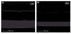
图3-6所示的结构虽然可以实现触控搭接,但当第二搭接层130膜层高度不够或其他膜层过高时,衬底基板100和封装盖板200对盒时,容易在第二搭接层130和第一搭接层230之间留下空隙,导致接触不良,进而影响触控信号的有效传递,无法实现准确的触控。如图11所示,为该结构第一搭接层230和第二搭接层130的接触效果图,由图中可以看出,第一搭接层230和第二搭接层130之间具有空隙,二者会导致触控障碍。Although the structure shown in FIGS. 3-6 can realize touch bonding, when the film height of the
在本实施例中,为了避免接触不良,第二搭接层130设置为两层,即包括依次层叠设置的第一透明导电氧化物层132和第一金属层133,参考图6,第一金属层133与对应的第一搭接层230接触。也就是说,第一透明导电氧化物层132位于下层,覆盖在支撑层120上,第一金属层133位于上层,覆盖在第一透明导电氧化物层132上,直接与对应的第一搭接层230接触。In this embodiment, in order to avoid poor contact, the
具体而言,发光器件包括阳极160、有机发光层190和阴极101,阳极160包括由下至上依次层叠设置的第二透明导电氧化物层161、第二金属层162和第四透明导电氧化物层163;其中,第二搭接层130的第一透明导电氧化物层132与发光器件的第二透明导电氧化物层161同层设置,第二搭接层130的第一金属层133和发光器件的的第二金属层162同层设置。此处,同层设置是指采用相同材料通过同一步构图工艺形成。具体的,第一透明导电氧化物层132材料可以是ITO,第一金属层133材料可以是Ag。Specifically, the light-emitting device includes an
如此设置的原因是,由于第一金属层133上不再覆盖其他膜层(如ITO),在显示面板对盒后的制备工艺的加热阶段,第一金属层133将会继续生长,直至与上方的第一搭接层230接触,使得第一金属层133和第一搭接层230之间不再有空隙,确保完全接触。而且,该结构的第二搭接层130仍然可以与阳极160通过同步构图工艺形成,仅需要剥离第一金属层133上方的透明导电氧化物层即可。关于制备方法,后续会进行详细说明。The reason for this setting is that since the
在本实施方式中,第二搭接层130和触控信号线140之间可以通过引线150实现电连接,即引线150一端电连接第二搭接层130,另一端电连接触控信号线140,如图6所示。引线150和触控信号线140均可以采用现有膜层(例如栅极层等)进行走线设计。在如图所示的实施例中,引线150设置于衬底基板100上且未被平坦层110覆盖,其位于支撑层120远离显示区的一侧,第二搭接层130覆盖在支撑层120上且向远离显示区的方向延伸并覆盖在引线150上,使得第二搭接层130和引线150直接接触,通过引线150将第二搭接层130和触控信号线140连接。在其他实施例中,第二搭接层130也可以不直接覆盖在引线150上,而是通过过孔与引线150进行电连接,也可以实现与触控信号线140电连接。引线150可以根据衬底基板100的各种走线的实际情况进行具体设计,此处不再赘述。In this embodiment, the electrical connection between the
如图3-6所示的结构中,封装盖板200的显示区还包括设置在触控电极层210远离盖板一侧的绝缘层220,利用绝缘层220将触控电极层210和发光器件的阴极101隔开,防止触控信号和阴极101信号互相干扰。封装盖板200和衬底基板100之间还设置有封装胶240,用于阻挡水氧入侵。In the structure shown in FIGS. 3-6 , the display area of the
本申请实施方式还提供一种触控显示面板的制备方法,参考图7所示的流程图,包括:The embodiment of the present application also provides a method for manufacturing a touch display panel, referring to the flowchart shown in FIG. 7 , including:
步骤S100,提供一衬底基板100和封装盖板200,衬底基板100和封装盖板200均包括显示区和围绕显示区设置的周边区;Step S100, providing a
步骤S200,在封装盖板200的显示区形成触控电极层210,采用导电材料在封装盖板200的周边区形成第一搭接层230,第一搭接层230连接触控电极层210;Step S200, forming a
步骤S300,在衬底基板100的周边区形成支撑层120和触控信号线140;Step S300, forming the supporting
步骤S400,采用导电材料在衬底基板100的周边区形成覆盖支撑层120的第二搭接层130,且使触控信号线140与第二搭接层130电连接;Step S400, using conductive material to form a
步骤S500,将衬底基板100和封装盖板200对盒,使第二搭接层130与第一搭接层230接触。In step S500 , the
以如图3-6所示的结构为例,步骤S100中,衬底基板100上通常形成有位于显示区的TFT阵列,还可以形成平坦层110以对衬底基板100进行平坦化。Taking the structure shown in FIGS. 3-6 as an example, in step S100 , a TFT array located in the display area is usually formed on the
步骤S200中,触控电极层210的形成根据其具体结构进行,当其为自电容式触控结构时,将第一触控电极层211和第二触控电极层212均在同一层形成,当其为互电容式触控结构时,依次形成第一触控电极层211、绝缘层220和第二触控电极层212。具体制备此处不再赘述。需要说明的是,触控电极层210还需延伸至封装盖板200的周边区,以与位于周边区的触控搭接部电连接。第一搭接层230可以与第一触控电极层211或第二触控电极层212通过同步构图工艺形成。In step S200, the
进一步地,该步骤还包括在触控电极层210上形成绝缘层220,以使后续对盒后触控电极层210和发光器件的阴极101相互绝缘。Further, this step also includes forming an insulating
步骤S300中,支撑层120制备方法可以根据材料进行选择,例如,当其为无机材料时可以采用沉积法等方法,当其为有机材料时可以采用蒸镀等方法,制备高度根据需要设计。In step S300, the preparation method of the
步骤S400中,第二搭接层130采用与发光器件的阳极160相同的材料时,可以与发光器件的阳极160通过一个掩膜版同步形成,由此可以得到图3-图5所示的结构。当需要形成图6所示的结构时,第二搭接层130仍然能与发光器件的阳极160同步形成,但需要增加一道工序用于去除最上层的透明导电氧化物层。In step S400, when the
具体的,发光器件的形成通常包括:在平坦层110上形成各子像素对应的阳极160,再形成像素界定层170定义各子像素的开口区,并在像素定义层上形成隔垫物180,然后在开口区内蒸镀相应的发光层190,最后形成覆盖整个显示区的阴极101。Specifically, the formation of the light emitting device generally includes: forming an
以阳极材料为ITO/Ag/ITO为例,形成发光器件的阳极和第二搭接层130包括以下步骤:Taking the anode material as ITO/Ag/ITO as an example, forming the anode of the light-emitting device and the
步骤S01,在衬底基板100上通过同步构图工艺形成位于显示区的第二透明导电氧化物层161(ITO)和位于周边区的第一透明导电氧化物层132(ITO);Step S01, forming a second transparent conductive oxide layer 161 (ITO) in the display area and a first transparent conductive oxide layer 132 (ITO) in the peripheral area on the
步骤S02,通过同步构图工艺形成位于显示区的第二金属层162(Ag)和位于周边区的第一金属层133(Ag);Step S02, forming the second metal layer 162 (Ag) in the display area and the first metal layer 133 (Ag) in the peripheral area through a simultaneous patterning process;
步骤S03,通过同步构图工艺形成位于显示区的第四透明导电氧化物层163(ITO)和位于所述周边区的第三透明导电氧化物层134(ITO);Step S03, forming the fourth transparent conductive oxide layer 163 (ITO) in the display area and the third transparent conductive oxide layer 134 (ITO) in the peripheral area through a simultaneous patterning process;
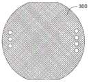
步骤S04,采用光刻工艺去除第三透明导电氧化物层134。由于该步骤中仅需要去除第二搭接层130最上层的ITO层,因此可以采用光刻掩膜工艺,此步骤掩膜板300结构如图8所示,该掩膜板300在衬底基板100周边区的对应位置具有开口。具体的,现在衬底基板100上涂覆光刻胶,通过光刻工艺将支撑层120顶起位置的第三透明导电氧化物层134刻蚀掉,暴露出第一金属层133。该步骤中,刻蚀采用干法刻蚀,避免刻蚀液影响下方的金属层,光刻和剥离的可参考图9-图10所示。In step S04, the third transparent
步骤S05,对第一金属层133进行加热,使Ag继续生长并能与第一搭接层230接触。对第一金属层133加热可以通过面板后续制备步骤中现有的加热步骤实现,以简化制备工艺。例如在制备隔垫物180时,会采用加热方式对隔垫物180进行固化,在此步骤中Ag会受热生长;在对衬底基板100和封装盖板200对盒后进行Frit封装时,也会采用加热方式对封装胶240进行固化,在此步骤中Ag也会受热生长。在这些步骤中,Ag都会生长使得最终与第一搭接层230紧密的贴合在一起。Step S05 , heating the
第二搭接层130采用双层结构相比采用三层结构,在整个制备过程中仅仅在衬底基板100制备过程中增加了的一道掩膜工艺,该工艺位于阳极蒸镀后,不需要对衬底基板100显示区和封装盖板200的制备进行任何改动,工艺简单,易于实施。The
图11分别示出了不同结构的第二搭接层130在与第一搭接层230对盒后的扫描电镜图,图中(a)表示第二搭接层为三层结构时的接触效果,明显可以看到中间的缝隙。图中(b)表示上述方法制备的双层结构的接触效果,可以看出支撑层120和第二搭接层130的总厚度约为3.95μm,第一搭接层230和第二搭接层130之间不再具有空隙,二者实现了良好的接触。Fig. 11 shows the scanning electron micrographs of the
图12分别示出了不同结构时Ag的透射电镜图,图中(a)表示第二搭接层为三层结构时的Ag层,图中(b)表示第二搭接层为双层结构时的Ag层。由图可知,上述方法制备的双层结构中Ag层厚度明显增加,说明Ag层确实得到了生长。Figure 12 shows the transmission electron microscope images of Ag in different structures, in which (a) represents the Ag layer when the second bonding layer is a three-layer structure, and (b) represents that the second bonding layer is a double-layer structure When the Ag layer. It can be seen from the figure that the thickness of the Ag layer in the double-layer structure prepared by the above method is obviously increased, indicating that the Ag layer has indeed been grown.
本申请实施方式还提供一种显示装置,该显示装置包括上述实施方式的触控显示面板。由于该显示装置具有上述触控显示面板,因此具有相同的有益效果,本申请在此不再赘述。Embodiments of the present application further provide a display device, which includes the touch display panel of the above embodiments. Since the display device has the above-mentioned touch display panel, it has the same beneficial effects, and the present application will not repeat them here.
本申请对于显示装置的适用不做具体限制,其可以是电视机、笔记本电脑、平板电脑、可穿戴显示设备、手机、车载显示、导航、电子书、数码相框、广告灯箱等任何具有显示功能的产品或部件。This application does not specifically limit the application of display devices, which can be TVs, notebook computers, tablet computers, wearable display devices, mobile phones, vehicle displays, navigation, e-books, digital photo frames, advertising light boxes, etc. product or part.
虽然本说明书中使用相对性的用语,例如“上”“下”来描述图标的一个组件对于另一组件的相对关系,但是这些术语用于本说明书中仅出于方便,例如根据附图中所述的示例的方向。能理解的是,如果将图标的装置翻转使其上下颠倒,则所叙述在“上”的组件将会成为在“下”的组件。当某结构在其它结构“上”时,有可能是指某结构一体形成于其它结构上,或指某结构“直接”设置在其它结构上,或指某结构通过另一结构“间接”设置在其它结构上。Although relative terms such as "upper" and "lower" are used in this specification to describe the relative relationship of one component of an icon to another component, these terms are used in this specification only for convenience, for example, according to the description in the accompanying drawings directions for the example described above. It will be appreciated that if the illustrated device is turned over so that it is upside down, then elements described as being "upper" will become elements that are "lower". When a structure is "on" another structure, it may mean that a structure is integrally formed on another structure, or that a structure is "directly" placed on another structure, or that a structure is "indirectly" placed on another structure through another structure. other structures.
用语“一个”、“一”、“该”、“所述”和“至少一个”用以表示存在一个或多个要素/组成部分/等;用语“包括”和“具有”用以表示开放式的包括在内的意思并且是指除了列出的要素/组成部分/等之外还可存在另外的要素/组成部分/等。The terms "a", "an", "the", "said" and "at least one" are used to indicate the presence of one or more elements/components/etc; the terms "comprising" and "have" are used to indicate an open The inclusive meaning and means that additional elements/components/etc. may be present in addition to the listed elements/components/etc.
本领域技术人员在考虑说明书及实践这里公开的发明后,将容易想到本申请的其它实施方案。本申请旨在涵盖本申请的任何变型、用途或者适应性变化,这些变型、用途或者适应性变化遵循本申请的一般性原理并包括本申请未公开的本技术领域中的公知常识或惯用技术手段。说明书和实施例仅被视为示例性的,本申请的真正范围和精神由所附的权利要求指出。Other embodiments of the present application will be readily apparent to those skilled in the art from consideration of the specification and practice of the invention disclosed herein. This application is intended to cover any modification, use or adaptation of the application, these modifications, uses or adaptations follow the general principles of the application and include common knowledge or conventional technical means in the technical field not disclosed in the application . The specification and examples are to be considered exemplary only, with a true scope and spirit of the application indicated by the appended claims.
Claims (9)
Translated fromChinesePriority Applications (2)
| Application Number | Priority Date | Filing Date | Title |
|---|---|---|---|
| CN202310316262.8ACN116367658A (en) | 2020-03-30 | 2020-03-30 | Touch display panel and display device |
| CN202010234947.4ACN111403463B (en) | 2020-03-30 | 2020-03-30 | Touch display panel, manufacturing method thereof and display device |
Applications Claiming Priority (1)
| Application Number | Priority Date | Filing Date | Title |
|---|---|---|---|
| CN202010234947.4ACN111403463B (en) | 2020-03-30 | 2020-03-30 | Touch display panel, manufacturing method thereof and display device |
Related Child Applications (1)
| Application Number | Title | Priority Date | Filing Date |
|---|---|---|---|
| CN202310316262.8ADivisionCN116367658A (en) | 2020-03-30 | 2020-03-30 | Touch display panel and display device |
Publications (2)
| Publication Number | Publication Date |
|---|---|
| CN111403463A CN111403463A (en) | 2020-07-10 |
| CN111403463Btrue CN111403463B (en) | 2023-04-28 |
Family
ID=71414131
Family Applications (2)
| Application Number | Title | Priority Date | Filing Date |
|---|---|---|---|
| CN202310316262.8APendingCN116367658A (en) | 2020-03-30 | 2020-03-30 | Touch display panel and display device |
| CN202010234947.4AActiveCN111403463B (en) | 2020-03-30 | 2020-03-30 | Touch display panel, manufacturing method thereof and display device |
Family Applications Before (1)
| Application Number | Title | Priority Date | Filing Date |
|---|---|---|---|
| CN202310316262.8APendingCN116367658A (en) | 2020-03-30 | 2020-03-30 | Touch display panel and display device |
Country Status (1)
| Country | Link |
|---|---|
| CN (2) | CN116367658A (en) |
Families Citing this family (4)
| Publication number | Priority date | Publication date | Assignee | Title |
|---|---|---|---|---|
| US12219825B2 (en) | 2021-02-09 | 2025-02-04 | Boe Technology Group Co., Ltd. | Display substrate and method for manufacturing the same, and display device |
| CN113054140B (en)* | 2021-03-18 | 2022-10-21 | 昆山国显光电有限公司 | Display panel, preparation method thereof and display device |
| CN113407058A (en)* | 2021-06-23 | 2021-09-17 | 昆山国显光电有限公司 | Touch control display panel |
| CN116075198A (en)* | 2023-02-24 | 2023-05-05 | 武汉天马微电子有限公司 | Display panel and display device |
Family Cites Families (5)
| Publication number | Priority date | Publication date | Assignee | Title |
|---|---|---|---|---|
| CN105158955B (en)* | 2015-10-26 | 2019-02-12 | 天马微电子股份有限公司 | Display panel and manufacturing method thereof |
| CN106229332B (en)* | 2016-09-21 | 2019-04-05 | 上海天马微电子有限公司 | Display panel, manufacturing method thereof and flexible display device |
| CN107068720B (en)* | 2017-04-19 | 2019-08-27 | 上海天马微电子有限公司 | Organic light-emitting diode display panel and display device |
| CN107092400B (en)* | 2017-06-27 | 2019-10-01 | 上海天马微电子有限公司 | Touch display panel and touch display device comprising same |
| CN107342370B (en)* | 2017-07-06 | 2019-05-07 | 武汉天马微电子有限公司 | Display panel and display device |
- 2020
- 2020-03-30CNCN202310316262.8Apatent/CN116367658A/enactivePending
- 2020-03-30CNCN202010234947.4Apatent/CN111403463B/enactiveActive
Also Published As
| Publication number | Publication date |
|---|---|
| CN111403463A (en) | 2020-07-10 |
| CN116367658A (en) | 2023-06-30 |
Similar Documents
| Publication | Publication Date | Title |
|---|---|---|
| CN111403463B (en) | Touch display panel, manufacturing method thereof and display device | |
| CN108231800B (en) | A kind of flexible display panels and preparation method thereof, display device | |
| CN107994036B (en) | Substrate and preparation method thereof, display panel, display device | |
| US11641772B2 (en) | Display device | |
| CN107665902B (en) | Organic light-emitting display and method of making the same | |
| US11522039B2 (en) | Stretchable display panel and display device | |
| CN110308822B (en) | Touch display panel and manufacturing method thereof | |
| CN111796718A (en) | Touch display panel, preparation method thereof, and display device | |
| WO2021081765A1 (en) | Display substrate, preparation method therefor, and display device | |
| WO2021258462A1 (en) | Display panel and display device | |
| CN107203296A (en) | Display panel, manufacturing method thereof and display device | |
| CN103677406B (en) | Touch panel and touch display panel | |
| CN111900192B (en) | Display panel and display device | |
| WO2021217793A1 (en) | Organic light emitting display and manufacturing method therefor | |
| CN111208916B (en) | Touch display panel and display device | |
| CN112310183B (en) | Display substrate and preparation method thereof, display device | |
| WO2020118910A1 (en) | Touch display device and manufacturing method therefor | |
| WO2021248453A1 (en) | Display panel and manufacturing method therefor, and display apparatus | |
| KR101721259B1 (en) | Electrostatic capacity type touch screen panel and method of manufacturing the same | |
| JP2025519304A (en) | Display panel and display device | |
| WO2023225957A9 (en) | Display panel and display device | |
| CN114840098A (en) | Touch display panel and manufacturing method thereof, touch display screen and spliced screen | |
| US11392258B2 (en) | Touch panel including dielectric structure, display panel and display device | |
| CN116472514A (en) | Array substrate and display device | |
| WO2021159293A1 (en) | Display panel, display device, and manufacturing method of display panel |
Legal Events
| Date | Code | Title | Description |
|---|---|---|---|
| PB01 | Publication | ||
| PB01 | Publication | ||
| SE01 | Entry into force of request for substantive examination | ||
| SE01 | Entry into force of request for substantive examination | ||
| GR01 | Patent grant | ||
| GR01 | Patent grant |