CN111403283A - Embedded germanium silicon fabrication method and embedded germanium silicon structure - Google Patents
Embedded germanium silicon fabrication method and embedded germanium silicon structureDownload PDFInfo
- Publication number
- CN111403283A CN111403283ACN202010138897.XACN202010138897ACN111403283ACN 111403283 ACN111403283 ACN 111403283ACN 202010138897 ACN202010138897 ACN 202010138897ACN 111403283 ACN111403283 ACN 111403283A
- Authority
- CN
- China
- Prior art keywords
- gate
- silicon germanium
- embedded
- germanium
- angstroms
- Prior art date
- Legal status (The legal status is an assumption and is not a legal conclusion. Google has not performed a legal analysis and makes no representation as to the accuracy of the status listed.)
- Pending
Links
- LEVVHYCKPQWKOP-UHFFFAOYSA-N[Si].[Ge]Chemical compound[Si].[Ge]LEVVHYCKPQWKOP-UHFFFAOYSA-N0.000titleclaimsabstractdescription125
- 238000004519manufacturing processMethods0.000titleclaimsabstractdescription31
- 238000000034methodMethods0.000titleclaimsdescription38
- 229910000577Silicon-germaniumInorganic materials0.000claimsabstractdescription129
- 238000005530etchingMethods0.000claimsabstractdescription58
- 230000004888barrier functionEffects0.000claimsabstractdescription38
- 239000000758substrateSubstances0.000claimsabstractdescription10
- 239000004065semiconductorSubstances0.000claimsabstractdescription9
- 125000006850spacer groupChemical group0.000claimsabstractdescription8
- 238000004140cleaningMethods0.000claimsabstractdescription7
- 238000000407epitaxyMethods0.000claimsabstractdescription5
- XUIMIQQOPSSXEZ-UHFFFAOYSA-NSiliconChemical compound[Si]XUIMIQQOPSSXEZ-UHFFFAOYSA-N0.000description12
- 229910052710siliconInorganic materials0.000description12
- 239000010703siliconSubstances0.000description12
- 230000008569processEffects0.000description11
- 230000015572biosynthetic processEffects0.000description7
- 238000010586diagramMethods0.000description7
- WGTYBPLFGIVFAS-UHFFFAOYSA-Mtetramethylammonium hydroxideChemical compound[OH-].C[N+](C)(C)CWGTYBPLFGIVFAS-UHFFFAOYSA-M0.000description6
- 229910052581Si3N4Inorganic materials0.000description5
- 239000010408filmSubstances0.000description5
- 229910052732germaniumInorganic materials0.000description5
- GNPVGFCGXDBREM-UHFFFAOYSA-Ngermanium atomChemical compound[Ge]GNPVGFCGXDBREM-UHFFFAOYSA-N0.000description5
- HQVNEWCFYHHQES-UHFFFAOYSA-Nsilicon nitrideChemical compoundN12[Si]34N5[Si]62N3[Si]51N64HQVNEWCFYHHQES-UHFFFAOYSA-N0.000description5
- VYPSYNLAJGMNEJ-UHFFFAOYSA-NSilicium dioxideChemical compoundO=[Si]=OVYPSYNLAJGMNEJ-UHFFFAOYSA-N0.000description3
- 238000000231atomic layer depositionMethods0.000description3
- 238000005229chemical vapour depositionMethods0.000description3
- 229910052814silicon oxideInorganic materials0.000description3
- IJGRMHOSHXDMSA-UHFFFAOYSA-NAtomic nitrogenChemical compoundN#NIJGRMHOSHXDMSA-UHFFFAOYSA-N0.000description2
- 229910021419crystalline siliconInorganic materials0.000description2
- 238000000151depositionMethods0.000description2
- 230000008021depositionEffects0.000description2
- 150000002500ionsChemical class0.000description2
- 238000012986modificationMethods0.000description2
- 230000004048modificationEffects0.000description2
- 238000001039wet etchingMethods0.000description2
- 238000001312dry etchingMethods0.000description1
- 230000000694effectsEffects0.000description1
- 238000005040ion trapMethods0.000description1
- 238000001459lithographyMethods0.000description1
- 239000000463materialSubstances0.000description1
- 229910052757nitrogenInorganic materials0.000description1
- 229920002120photoresistant polymerPolymers0.000description1
- 239000013589supplementSubstances0.000description1
- 239000010409thin filmSubstances0.000description1
Images


Classifications
- H—ELECTRICITY
- H10—SEMICONDUCTOR DEVICES; ELECTRIC SOLID-STATE DEVICES NOT OTHERWISE PROVIDED FOR
- H10D—INORGANIC ELECTRIC SEMICONDUCTOR DEVICES
- H10D30/00—Field-effect transistors [FET]
- H10D30/01—Manufacture or treatment
- H10D30/021—Manufacture or treatment of FETs having insulated gates [IGFET]
- H—ELECTRICITY
- H10—SEMICONDUCTOR DEVICES; ELECTRIC SOLID-STATE DEVICES NOT OTHERWISE PROVIDED FOR
- H10D—INORGANIC ELECTRIC SEMICONDUCTOR DEVICES
- H10D30/00—Field-effect transistors [FET]
- H10D30/60—Insulated-gate field-effect transistors [IGFET]
- H10D30/791—Arrangements for exerting mechanical stress on the crystal lattice of the channel regions
- H10D30/797—Arrangements for exerting mechanical stress on the crystal lattice of the channel regions being in source or drain regions, e.g. SiGe source or drain
- H—ELECTRICITY
- H10—SEMICONDUCTOR DEVICES; ELECTRIC SOLID-STATE DEVICES NOT OTHERWISE PROVIDED FOR
- H10D—INORGANIC ELECTRIC SEMICONDUCTOR DEVICES
- H10D62/00—Semiconductor bodies, or regions thereof, of devices having potential barriers
- H10D62/10—Shapes, relative sizes or dispositions of the regions of the semiconductor bodies; Shapes of the semiconductor bodies
- H10D62/13—Semiconductor regions connected to electrodes carrying current to be rectified, amplified or switched, e.g. source or drain regions
- H10D62/149—Source or drain regions of field-effect devices
- H10D62/151—Source or drain regions of field-effect devices of IGFETs
- H—ELECTRICITY
- H10—SEMICONDUCTOR DEVICES; ELECTRIC SOLID-STATE DEVICES NOT OTHERWISE PROVIDED FOR
- H10D—INORGANIC ELECTRIC SEMICONDUCTOR DEVICES
- H10D84/00—Integrated devices formed in or on semiconductor substrates that comprise only semiconducting layers, e.g. on Si wafers or on GaAs-on-Si wafers
- H10D84/01—Manufacture or treatment
- H10D84/0123—Integrating together multiple components covered by H10D12/00 or H10D30/00, e.g. integrating multiple IGBTs
- H10D84/0126—Integrating together multiple components covered by H10D12/00 or H10D30/00, e.g. integrating multiple IGBTs the components including insulated gates, e.g. IGFETs
- H10D84/013—Manufacturing their source or drain regions, e.g. silicided source or drain regions
- H—ELECTRICITY
- H10—SEMICONDUCTOR DEVICES; ELECTRIC SOLID-STATE DEVICES NOT OTHERWISE PROVIDED FOR
- H10D—INORGANIC ELECTRIC SEMICONDUCTOR DEVICES
- H10D84/00—Integrated devices formed in or on semiconductor substrates that comprise only semiconducting layers, e.g. on Si wafers or on GaAs-on-Si wafers
- H10D84/01—Manufacture or treatment
- H10D84/02—Manufacture or treatment characterised by using material-based technologies
- H10D84/03—Manufacture or treatment characterised by using material-based technologies using Group IV technology, e.g. silicon technology or silicon-carbide [SiC] technology
- H10D84/038—Manufacture or treatment characterised by using material-based technologies using Group IV technology, e.g. silicon technology or silicon-carbide [SiC] technology using silicon technology, e.g. SiGe
- H—ELECTRICITY
- H10—SEMICONDUCTOR DEVICES; ELECTRIC SOLID-STATE DEVICES NOT OTHERWISE PROVIDED FOR
- H10D—INORGANIC ELECTRIC SEMICONDUCTOR DEVICES
- H10D84/00—Integrated devices formed in or on semiconductor substrates that comprise only semiconducting layers, e.g. on Si wafers or on GaAs-on-Si wafers
- H10D84/80—Integrated devices formed in or on semiconductor substrates that comprise only semiconducting layers, e.g. on Si wafers or on GaAs-on-Si wafers characterised by the integration of at least one component covered by groups H10D12/00 or H10D30/00, e.g. integration of IGFETs
- H10D84/82—Integrated devices formed in or on semiconductor substrates that comprise only semiconducting layers, e.g. on Si wafers or on GaAs-on-Si wafers characterised by the integration of at least one component covered by groups H10D12/00 or H10D30/00, e.g. integration of IGFETs of only field-effect components
- H10D84/83—Integrated devices formed in or on semiconductor substrates that comprise only semiconducting layers, e.g. on Si wafers or on GaAs-on-Si wafers characterised by the integration of at least one component covered by groups H10D12/00 or H10D30/00, e.g. integration of IGFETs of only field-effect components of only insulated-gate FETs [IGFET]
Landscapes
- Metal-Oxide And Bipolar Metal-Oxide Semiconductor Integrated Circuits (AREA)
- Insulated Gate Type Field-Effect Transistor (AREA)
Abstract
Translated fromChinese
Description
Translated fromChinese技术领域technical field
本发明涉及半导体领域,特别是涉及一种用于半导体器件生产中的嵌入式锗硅制作方法。本发明还涉及一种用于半导体器件生产中的嵌入式锗硅结构。The invention relates to the field of semiconductors, in particular to a method for manufacturing embedded silicon germanium used in the production of semiconductor devices. The invention also relates to an embedded silicon germanium structure for use in the production of semiconductor devices.
背景技术Background technique
在半导体制造工艺中,为提高PMOS器件载流子迁移率,业界普通采用锗硅沉积技术。现有技术中制作SIGMA型锗硅沟槽的方法包括以下步骤:在衬底上形成有源层;在有源层上形成晶硅栅极层;形成晶硅栅极侧墙;形成锗硅硬掩模层;锗硅光刻;锗硅干法刻蚀形成U型沟槽;光刻胶干法剥离和湿法清洗;TMAH处理形成SIGMA型锗硅沟槽;锗硅外延沉积,参考图1至图3所示。In the semiconductor manufacturing process, in order to improve the carrier mobility of the PMOS device, the silicon germanium deposition technology is generally used in the industry. The method for fabricating a SIGMA-type silicon-germanium trench in the prior art includes the following steps: forming an active layer on a substrate; forming a crystalline silicon gate layer on the active layer; forming a crystalline silicon gate spacer; Mask layer; GeSi lithography; GeSi dry etching to form U-shaped trenches; Photoresist dry stripping and wet cleaning; TMAH treatment to form SIGMA SiGe trenches; GeSi epitaxial deposition, refer to Figure 1 as shown in Figure 3.
现有的PMOS嵌入式锗硅尖端距离沟道之间的距离T2G(tip to gate)受限于硅到栅极之间的距离S2G(silicon to gate)以及沟槽深度,导致T2G不能现继续缩小,这就限制了锗硅对沟道的应力的提升。The distance T2G (tip to gate) between the existing PMOS embedded silicon germanium tip and the channel is limited by the distance S2G (silicon to gate) between the silicon and the gate and the depth of the trench, so that the T2G cannot continue to shrink. , which limits the increase of SiGe stress on the channel.
发明内容SUMMARY OF THE INVENTION
在发明内容部分中引入了一系列简化形式的概念,该简化形式的概念均为本领域现有技术简化,这将在具体实施方式部分中进一步详细说明。本发明的发明内容部分并不意味着要试图限定出所要求保护的技术方案的关键特征和必要技术特征,更不意味着试图确定所要求保护的技术方案的保护范围。A series of concepts in simplified form are introduced in the summary of the invention, and the concepts in the simplified form are all simplifications of the prior art in the art, which will be further described in detail in the detailed description. The Summary of the Invention section of the present invention is not intended to attempt to limit the key features and essential technical features of the claimed technical solution, nor is it intended to attempt to determine the protection scope of the claimed technical solution.
本发明要解决的技术问题是提供一种保持嵌入式锗硅结构侧墙厚度、锗硅硬掩膜刻蚀阻挡层厚度和锗硅沟槽最终深度等参数都不变的情况下,能减小到栅极之间的距离(S2G)的嵌入式锗硅制作方法。The technical problem to be solved by the present invention is to provide a method that can reduce the thickness of the sidewall of the embedded germanium-silicon structure, the thickness of the silicon-germanium hard mask etching barrier layer and the final depth of the germanium-silicon trench and other parameters. Embedding silicon germanium fabrication method for distance to gate (S2G).
本发明要解决的另一技术问题是提供一种保持嵌入式锗硅结构侧墙厚度、锗硅硬掩膜刻蚀阻挡层厚度和锗硅沟槽最终深度等参数都不变的情况下,能提高锗硅对沟道的应力,并能增大锗硅体积的嵌入式锗硅结构。Another technical problem to be solved by the present invention is to provide a method that can maintain the parameters such as the thickness of the sidewall of the embedded germanium-silicon structure, the thickness of the silicon-germanium hard mask etching barrier layer, and the final depth of the germanium-silicon trench. An embedded silicon germanium structure that increases the stress of silicon germanium on the channel and can increase the volume of silicon germanium.
为解决上述技术问题,本发明提供一种用于包括但不限于PMOS器件制作工艺的嵌入式锗硅制作方法,包括以下步骤:In order to solve the above technical problems, the present invention provides an embedded silicon germanium fabrication method including but not limited to a PMOS device fabrication process, comprising the following steps:
S1,在半导体衬底上依次生成有源区、栅极、栅极绝缘层和锗硅硬掩膜刻蚀阻挡层;其中,步骤S1中生成有源区、栅极、栅极绝缘层和锗硅硬掩膜刻蚀阻挡层的工艺均可以采用现有工艺技术实现;S1, an active region, a gate, a gate insulating layer and a silicon germanium hard mask etching barrier are sequentially generated on the semiconductor substrate; wherein, in step S1, an active region, a gate, a gate insulating layer and a germanium are generated The process of etching the barrier layer of the silicon hard mask can be realized by the existing process technology;
可选择的,所述锗硅硬掩膜刻蚀阻挡层自上而下依次包含原子层沉积氮化硅、原子层氧化硅薄膜;Optionally, the silicon germanium hard mask etching barrier layer sequentially includes atomic layer deposition silicon nitride and atomic layer silicon oxide film from top to bottom;
可选择的,所述栅极两侧形成侧墙以及顶部的化学气相沉积氮化硅薄膜;Optionally, sidewalls are formed on both sides of the gate and a chemical vapor deposition silicon nitride film is formed on the top;
可选择的,有源区带有P型浅掺杂的N离子阱;Optionally, the active region has a P-type shallowly doped N ion well;
S2,执行刻蚀,在两栅极之间的有源区中形成截面为坛形的浅沟槽,所述浅沟槽侧壁的一部分位于所述锗硅硬掩膜刻蚀阻挡层和栅极侧墙正下方;其中,所述坛形包括但不限于中间大两端小的常见坛形。S2, perform etching to form a shallow trench with an altar-shaped cross-section in the active region between the two gates, and a part of the sidewall of the shallow trench is located on the silicon germanium hard mask etching barrier layer and the gate Right below the pole side wall; wherein, the altar shape includes but is not limited to the common altar shape with large middle and small ends.
可选择的,步骤S2包括以下子步骤;Optionally, step S2 includes the following sub-steps;
S2.1,第一次刻蚀,形成所述浅沟槽的上半部,使L1<T1+T2,L1是浅沟槽侧壁顶点与栅极之间距离,T1是栅极侧墙厚度,T2是锗硅硬掩膜刻蚀阻挡层厚度;S2.1, the first etching to form the upper half of the shallow trench, so that L1<T1+T2, L1 is the distance between the top of the sidewall of the shallow trench and the gate, and T1 is the thickness of the gate sidewall , T2 is the thickness of the silicon germanium hard mask etching barrier;
S2.2,第二次刻蚀,形成所述浅沟槽的下半部。S2.2, a second etching to form the lower half of the shallow trench.
可选择的,所述浅沟槽的上半部为一倒置的碗形结构,所述浅沟槽的下半部为一正置碗形结构,所述倒置的碗形结构和正置碗形结构的碗口相接形成所述坛形浅沟槽。Optionally, the upper half of the shallow groove is an inverted bowl-shaped structure, the lower half of the shallow groove is an upright bowl-shaped structure, the inverted bowl-shaped structure and the upright bowl-shaped structure The bowl mouths are connected to form the altar-shaped shallow groove.
可选择的,所述第一次刻蚀采用各向同性等离子体对所述有源区进行横向和纵向刻蚀;Optionally, the first etching uses isotropic plasma to perform lateral and vertical etching on the active region;
所述第二次刻蚀采用各向异性等离子体对所述有源区进行纵向刻蚀。The second etching uses anisotropic plasma to longitudinally etch the active region.
可选择的,所述第一次刻蚀参数范围为5~20mt/3~600w/T/Bias0~300V/5~150CF4/5~10s;Optionally, the parameter range of the first etching is 5~20mt/3~600w/T/Bias0~300V/5~150CF4/5~10s;
所述第二次刻蚀参数范围为20~50mt/200~500w/200~600v/2~10O2/150~350HBr/150~300He/30~50s。The second etching parameter range is 20-50mt/200-500w/200-600v/2-10O2/150-350HBr/150-300He/30-50s.
S3,清洗去除刻蚀残留物;S3, cleaning to remove the etching residue;
可选择的,采用湿法清洗去除刻蚀残留物。Alternatively, wet cleaning is used to remove etching residues.
S4,刻蚀所述浅沟槽形成sigma型深沟槽,所述sigma型深沟槽顶部的一部分与所述硅硬掩膜刻蚀阻挡层或栅极侧墙相邻,所述sigma型深沟槽两侧分别形成有向外延伸的尖端,所述尖端位于栅极正下方的有源区中;S4, etch the shallow trench to form a sigma deep trench, a part of the top of the sigma deep trench is adjacent to the silicon hard mask etch barrier or gate spacer, and the sigma deep trench is Two sides of the trench are respectively formed with outwardly extending tips, and the tips are located in the active region just below the gate;
可选择的,采用湿法刻蚀所述坛形浅沟槽形成sigma型深沟槽,湿法刻蚀采用四甲基氢氧化铵溶液。Optionally, a sigma-type deep trench is formed by wet etching the altar-shaped shallow trench, and a tetramethylammonium hydroxide solution is used for the wet etching.
S5,在sigma型深沟槽内生长锗硅外延形成嵌入式锗硅区。所述sigma型深沟槽两侧的尖端经锗硅外延生长形成锗硅尖端;S5, growing SiGe epitaxy in the sigma type deep trench to form an embedded SiGe region. The tips on both sides of the sigma deep trench are epitaxially grown on germanium to form silicon germanium tips;
可选择的,所述嵌入式锗硅区两侧分别形成有向外延伸的锗硅尖端,所述锗硅尖端与其上方栅极竖直方向距离范围为100埃~200埃;Optionally, two sides of the embedded silicon germanium region are respectively formed with silicon germanium tips extending outward, and the vertical distance between the silicon germanium tip and the gate above it ranges from 100 angstroms to 200 angstroms;
所述嵌入式锗硅尖端与其上方栅极水平方向距离范围为-10埃~30埃;The horizontal distance between the embedded silicon germanium tip and the gate above it in the horizontal direction ranges from -10 angstroms to 30 angstroms;
所述嵌入式锗硅区深度范围为550埃~850埃。The depth of the embedded SiGe region ranges from 550 angstroms to 850 angstroms.
本发明提供一种用于包括但不限于PMOS器件制作工艺的嵌入式锗硅结构,包括:衬底上方形成的有源区,有源区上形成有栅极,栅极两侧形成有栅极侧墙,栅极顶部形成有栅极绝缘层,锗硅硬掩膜刻蚀阻挡层覆盖在栅极绝缘层和栅极侧墙上;The present invention provides an embedded silicon germanium structure including but not limited to a PMOS device fabrication process, comprising: an active region formed above a substrate, a gate formed on the active region, and gates formed on both sides of the gate sidewalls, a gate insulating layer is formed on the top of the gate, and a silicon germanium hard mask etching barrier layer covers the gate insulating layer and the gate sidewalls;
其中,两栅极之间的有源区中形成有嵌入式锗硅区,所述嵌入式锗硅区顶部的一部分与所述硅硬掩膜刻蚀阻挡层或栅极侧墙相邻,所述嵌入式锗硅区两侧分别形成有向外延伸的锗硅尖端,所述锗硅尖端位于栅极正下方的有源区中。Wherein, an embedded germanium silicon region is formed in the active region between the two gates, and a part of the top of the embedded germanium silicon region is adjacent to the silicon hard mask etching barrier layer or the gate sidewall, so Two sides of the embedded silicon germanium region are respectively formed with silicon germanium tips extending outward, and the silicon germanium tips are located in the active region just below the gate.
可选择的,L2<T1+T2,L2是嵌入式锗硅区侧壁顶点与栅极之间距离,T1是栅极侧墙厚度,T2是锗硅硬掩膜刻蚀阻挡层厚度。Optionally, L2<T1+T2, L2 is the distance between the apex of the sidewall of the embedded SiGe region and the gate, T1 is the thickness of the gate sidewall, and T2 is the thickness of the SiGe hard mask etching barrier layer.
可选择的,所述锗硅尖端与其上方栅极之间距离范围为100埃~200埃。Optionally, the distance between the silicon germanium tip and the gate above it ranges from 100 angstroms to 200 angstroms.
所述嵌入式锗硅区深度范围为550埃~850埃。The depth of the embedded SiGe region ranges from 550 angstroms to 850 angstroms.
本发明提供的嵌入式锗硅制作方法及嵌入式锗硅结构。在栅极侧墙及锗硅硬掩膜刻蚀阻挡层正下方有锗硅相邻,所述锗硅尖端到沟道的距离H2比现有的锗硅尖端到沟道的距离h2更小,所述锗硅尖端到栅极的距离T2G比现有的锗硅尖端到栅极的距离t2g更小。因此,所述锗硅的体积比现有的锗硅更大,所述锗硅的应力比现有的锗硅更大。本发明一方面提升了锗硅对沟道的应力,另一方面还增大了锗硅的体积,进一步的提升了锗硅对沟道的应力,从而提高PMOS器件性能。The invention provides an embedded silicon germanium fabrication method and an embedded silicon germanium structure. There are germanium-silicon adjacent to the gate sidewall and the silicon-germanium hard mask etching barrier layer, and the distance H2 between the germanium-silicon tip and the channel is smaller than the existing distance h2 from the germanium-silicon tip to the channel, The distance T2G from the silicon germanium tip to the gate is smaller than the existing distance t2g from the silicon germanium tip to the gate. Therefore, the volume of the SiGe is larger than that of the existing SiGe, and the stress of the SiGe is larger than that of the existing SiGe. The present invention improves the stress of silicon germanium on the channel on the one hand, and increases the volume of silicon germanium on the other hand, further improves the stress of silicon germanium on the channel, thereby improving the performance of the PMOS device.
附图说明Description of drawings
本发明附图旨在示出根据本发明的特定示例性实施例中所使用的方法、结构和/或材料的一般特性,对说明书中的描述进行补充。然而,本发明附图是未按比例绘制的示意图,因而可能未能够准确反映任何所给出的实施例的精确结构或性能特点,本发明附图不应当被解释为限定或限制由根据本发明的示例性实施例所涵盖的数值或属性的范围。下面结合附图与具体实施方式对本发明作进一步详细的说明:The drawings of the present invention are intended to supplement the description in the specification by illustrating the general characteristics of methods, structures and/or materials used in certain exemplary embodiments according to the present invention. However, the drawings of the present invention are schematic representations not to scale and thus may not accurately reflect the precise structural or performance characteristics of any given embodiment, and the drawings of the present invention should not be construed as limiting or limiting the scope of the invention in accordance with the present invention. The range of values or properties encompassed by the exemplary embodiments. The present invention will be described in further detail below in conjunction with the accompanying drawings and specific embodiments:
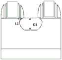
图1是现有技术嵌入式锗硅制作方法示意图一,其显示形成U形浅沟槽。FIG. 1 is a schematic diagram 1 of a prior art method for manufacturing an embedded silicon germanium, which shows the formation of a U-shaped shallow trench.
图2是现有技术嵌入式锗硅制作方法示意图二,其显示形成sigma型深沟槽。FIG. 2 is a second schematic diagram of a prior art method for manufacturing embedded silicon germanium, which shows the formation of a sigma type deep trench.
图3是现有技术嵌入式锗硅制作方法示意图三,其显示形成嵌入式锗硅区。FIG. 3 is a schematic diagram 3 of a prior art method for manufacturing an embedded silicon germanium, which shows the formation of an embedded silicon germanium region.
图4是本发明嵌入式锗硅制作方法流程示意图。FIG. 4 is a schematic flowchart of a method for manufacturing embedded silicon germanium according to the present invention.
图5是本发明嵌入式锗硅制作方法示意图一,其显示形成浅沟槽上半部分。FIG. 5 is a schematic diagram 1 of the method for fabricating the embedded silicon germanium according to the present invention, which shows the formation of the upper half of the shallow trench.
图6是本发明嵌入式锗硅制作方法示意图二,其显示形成坛形浅沟槽。FIG. 6 is a second schematic diagram of the method for manufacturing the embedded silicon germanium according to the present invention, which shows the formation of a shallow trench in the shape of an altar.
图7是本发明嵌入式锗硅制作方法示意图三,其显示形成sigma型深沟槽。FIG. 7 is a schematic diagram 3 of the method for manufacturing the embedded silicon germanium according to the present invention, which shows the formation of a sigma type deep trench.
图8是本发明嵌入式锗硅制作方法示意图三,其显示形成嵌入式锗硅外延区。FIG. 8 is a schematic diagram 3 of the method for manufacturing the embedded silicon germanium according to the present invention, which shows the formation of the embedded silicon germanium epitaxial region.
附图标记说明Description of reference numerals
1 是衬底1 is the substrate
2 是有源区2 is the active area
3 是栅极3 is the gate
4 是锗硅硬掩膜刻蚀阻挡层4 is the silicon germanium hard mask etch barrier
5 是栅极侧墙5 is the gate sidewall
6 是栅极绝缘层6 is the gate insulating layer
7 是现有技术U形浅沟槽7 is the prior art U-shaped shallow trench
8 是现有技术sigma型深沟槽8 is the prior art sigma type deep groove
9 是现有技术锗硅外延区9 is the prior art silicon germanium epitaxial region
10 是本发明浅沟槽的上半部10 is the upper half of the shallow trench of the present invention
11 是本发明锗硅外延区11 is the silicon germanium epitaxial region of the present invention
12 是本发明嵌入式锗硅区顶部与所述硅硬掩膜刻蚀阻挡层或栅极侧墙相邻的位置12 is the position where the top of the embedded germanium silicon region of the present invention is adjacent to the silicon hard mask etching barrier layer or gate spacer
13 是本发明锗硅尖端13 is the silicon germanium tip of the present invention
l1 是现有技术U形浅沟槽侧壁顶点与其旁侧栅极水平方向距离l1 is the horizontal distance between the vertex of the sidewall of the U-shaped shallow trench and its side gate in the prior art
d1 是现有技术U形浅沟槽深度d1 is the depth of the prior art U-shaped shallow trench
d2 是现有技术sigma型深沟槽深度d2 is the prior art sigma deep trench depth
h2 是现有技术锗硅尖端与其上方栅极竖直方向距离h2 is the vertical distance between the prior art GeSi tip and the gate above it
t2g 是现有技术锗硅尖端与其上方栅极水平方向距离t2g is the horizontal distance between the prior art SiGe tip and the gate above it
L1 是本发明浅沟槽侧壁顶点与其上方栅极水平方向距离L1 is the horizontal distance between the top of the sidewall of the shallow trench in the present invention and the gate above it
L2 是本发明嵌入式锗硅区侧壁顶点与其上方栅极水平方向距离L2 is the horizontal distance between the sidewall apex of the embedded SiGe region and the gate above it in the present invention
D1 是本发明坛形浅沟槽深度D1 is the depth of the altar-shaped shallow groove of the present invention
D2 是本发明sigma型深沟槽深度D2 is the depth of the sigma deep groove of the present invention
H2 是本发明锗硅尖端与其上方栅极竖直方向距离H2 is the vertical distance between the silicon germanium tip of the present invention and the gate above it
T2G 是本发明锗硅尖端与其上方栅极水平方向距离。T2G is the horizontal distance between the SiGe tip of the present invention and the gate above it.
具体实施方式Detailed ways
以下通过特定的具体实施例说明本发明的实施方式,本领域技术人员可由本说明书所公开的内容充分地了解本发明的其他优点与技术效果。本发明还可以通过不同的具体实施方式加以实施或应用,本说明书中的各项细节也可以基于不同观点加以应用,在没有背离发明总的设计思路下进行各种修饰或改变。需说明的是,在不冲突的情况下,以下实施例及实施例中的特征可以相互组合。本发明下述示例性实施例可以多种不同的形式来实施,并且不应当被解释为只限于这里所阐述的具体实施例。应当理解的是,提供这些实施例是为了使得本发明的公开彻底且完整,并且将这些示例性具体实施例的技术方案充分传达给本领域技术人员。The embodiments of the present invention are described below through specific specific embodiments, and those skilled in the art can fully understand other advantages and technical effects of the present invention from the contents disclosed in this specification. The present invention can also be implemented or applied through different specific embodiments, and various details in this specification can also be applied based on different viewpoints, and various modifications or changes can be made without departing from the general design idea of the invention. It should be noted that the following embodiments and features in the embodiments may be combined with each other under the condition of no conflict. The following exemplary embodiments of the present invention may be embodied in many different forms and should not be construed as limited to the specific embodiments set forth herein. It should be understood that these embodiments are provided so that this disclosure will be thorough and complete, and will fully convey the technical solutions of these exemplary embodiments to those skilled in the art.
如图4所示,本发明提供一种用于包括但不限于PMOS器件制作工艺的嵌入式锗硅制作方法第一实施例,包括以下步骤:As shown in FIG. 4 , the present invention provides a first embodiment of an embedded silicon germanium fabrication method including but not limited to a PMOS device fabrication process, including the following steps:
S1,在半导体衬底上依次生成有源区、栅极、栅极绝缘层和锗硅硬掩膜刻蚀阻挡层;其中,步骤S1中生成有源区、栅极、栅极绝缘层和锗硅硬掩膜刻蚀阻挡层的工艺均可以采用现有工艺技术实现,本发明不再赘述;S1, an active region, a gate, a gate insulating layer and a silicon germanium hard mask etching barrier are sequentially generated on the semiconductor substrate; wherein, in step S1, an active region, a gate, a gate insulating layer and a germanium are generated The process of etching the barrier layer of the silicon hard mask can be realized by using the existing process technology, which is not repeated in the present invention;
可选择的,所述锗硅硬掩膜刻蚀阻挡层自上而下依次包含原子层沉积氮化硅、原子层氧化硅薄膜;Optionally, the silicon germanium hard mask etching barrier layer sequentially includes atomic layer deposition silicon nitride and atomic layer silicon oxide film from top to bottom;
可选择的,所述栅极两侧形成侧墙以及顶部的化学气相沉积氮化硅薄膜;Optionally, sidewalls are formed on both sides of the gate and a chemical vapor deposition silicon nitride film is formed on the top;
可选择的,有源区带有P型浅掺杂的N离子阱;Optionally, the active region has a P-type shallowly doped N ion well;
S2,执行刻蚀,在两栅极之间的有源区中形成截面为坛形的浅沟槽,所述浅沟槽侧壁的一部分位于所述硅硬掩膜刻蚀阻挡层和栅极侧墙正下方;S2, perform etching to form a shallow trench with an altar-shaped cross-section in the active region between the two gates, and a portion of the sidewall of the shallow trench is located between the silicon hard mask etching barrier layer and the gate directly below the side wall;
S3,清洗去除刻蚀残留物;S3, cleaning to remove the etching residue;
S4,刻蚀所述浅沟槽形成sigma型深沟槽,所述sigma型深沟槽顶部的一部分与所述硅硬掩膜刻蚀阻挡层或栅极侧墙相邻,所述sigma型深沟槽两侧分别形成有向外延伸的尖端,所述尖端位于栅极正下方的有源区中;S4, etch the shallow trench to form a sigma deep trench, a part of the top of the sigma deep trench is adjacent to the silicon hard mask etch barrier or gate spacer, and the sigma deep trench is Two sides of the trench are respectively formed with outwardly extending tips, and the tips are located in the active region just below the gate;
S5,在sigma型深沟槽内生长锗硅外延形成嵌入式锗硅区,所述sigma型深沟槽两侧的尖端经锗硅外延生长形成锗硅尖端。S5 , growing SiGe epitaxy in the sigma-type deep trench to form an embedded SiGe region, and the tips on both sides of the sigma-type deep trench are epitaxially grown with SiGe to form SiGe tips.
本发明提供一种用于包括但不限于PMOS器件制作工艺的嵌入式锗硅制作方法第二实施例,包括以下步骤:The present invention provides a second embodiment of an embedded silicon germanium fabrication method including but not limited to a PMOS device fabrication process, including the following steps:
S1,在半导体衬底上依次生成有源区、栅极、栅极绝缘层和锗硅硬掩膜刻蚀阻挡层;其中,步骤S1中生成有源区、栅极、栅极绝缘层和锗硅硬掩膜刻蚀阻挡层的工艺均可以采用现有工艺技术实现;S1, an active region, a gate, a gate insulating layer and a silicon germanium hard mask etching barrier are sequentially generated on the semiconductor substrate; wherein, in step S1, an active region, a gate, a gate insulating layer and a germanium are generated The process of etching the barrier layer of the silicon hard mask can be realized by the existing process technology;
可选择的,所述锗硅硬掩膜刻蚀阻挡层自上而下依次包含原子层沉积氮化硅、原子层氧化硅薄膜;所述栅极两侧形成侧墙以及顶部的化学气相沉积氮化硅薄膜;有源区带有P型浅掺杂的N离子阱;Optionally, the silicon germanium hard mask etching barrier layer sequentially includes atomic layer deposition silicon nitride and atomic layer silicon oxide film from top to bottom; sidewalls are formed on both sides of the gate and chemical vapor deposition nitrogen is formed on the top. Silicon thin film; active region with P-type shallowly doped N ion trap;
S2,执行刻蚀,在两栅极之间的有源区中形成截面为坛形的浅沟槽,所述浅沟槽侧壁的一部分位于所述锗硅硬掩膜刻蚀阻挡层和栅极侧墙正下方;其中,所述坛形包括但不限于中间大两端小的常见坛形。S2, perform etching to form a shallow trench with an altar-shaped cross-section in the active region between the two gates, and a part of the sidewall of the shallow trench is located on the silicon germanium hard mask etching barrier layer and the gate Right below the pole side wall; wherein, the altar shape includes but is not limited to the common altar shape with large middle and small ends.
其中,步骤S2包括以下子步骤;Wherein, step S2 includes the following sub-steps;
S2.1,参考图5所示,采用各向同性等离子体对所述有源区进行横向和纵向刻蚀形成所述浅沟槽的上半部,刻蚀参数范围为5~20mt/3~600w/T/Bias0~300V/5~150CF4/5~10s,使L1<T1+T2,L1是浅沟槽侧壁顶点与栅极之间距离,T1是栅极侧墙厚度,T2是锗硅硬掩膜刻蚀阻挡层厚度;S2.1, as shown in FIG. 5 , use isotropic plasma to etch the active region laterally and vertically to form the upper half of the shallow trench, and the etching parameters range from 5 to 20mt/3~ 600w/T/Bias0~300V/5~150CF4/5~10s, so that L1<T1+T2, L1 is the distance between the top of the sidewall of the shallow trench and the gate, T1 is the thickness of the gate sidewall, T2 is the germanium silicon Hard mask etch barrier thickness;
S2.2,参考图6所示,采用各向异性等离子体对所述有源区进行纵向刻蚀形成所述浅沟槽的下半部,刻蚀参数范围为20~50mt/200~500w/200~600v/2~10O2/150~350HBr/150~300He/30~50s。S2.2, as shown in FIG. 6, the active region is longitudinally etched by anisotropic plasma to form the lower half of the shallow trench, and the etching parameters range from 20 to 50 mt/200 to 500 w/ 200~600v/2~10O2/150~350HBr/150~300He/30~50s.
所述浅沟槽的上半部为一倒置的碗形结构,所述浅沟槽的下半部为一正置碗形结构,所述倒置的碗形结构和正置碗形结构的碗口相接形成所述坛形浅沟槽。The upper half of the shallow groove is an inverted bowl-shaped structure, and the lower half of the shallow groove is an upright bowl-shaped structure. Then, the altar-shaped shallow groove is formed.
S3,采用湿法清洗去除刻蚀残留物。S3, using wet cleaning to remove etching residues.
S4,参考图7所示,采用四甲基氢氧化铵溶液刻蚀所述浅沟槽形成sigma型深沟槽,所述sigma型深沟槽顶部的一部分与所述锗硅硬掩膜刻蚀阻挡层或栅极侧墙相邻,所述sigma型深沟槽两侧分别形成有向外延伸的尖端,所述尖端位于栅极正下方的有源区中;S4 , as shown in FIG. 7 , the shallow trench is etched with tetramethyl ammonium hydroxide solution to form a sigma type deep trench, and a part of the top of the sigma type deep trench is etched with the silicon germanium hard mask The barrier layer or the gate spacer is adjacent, and outwardly extending tips are respectively formed on both sides of the sigma deep trench, and the tips are located in the active region directly below the gate;
S5,参考图8所示,在sigma型深沟槽内生长锗硅外延形成嵌入式锗硅区。所述sigma型深沟槽两侧的尖端经锗硅外延生长形成锗硅尖端;S5 , as shown in FIG. 8 , silicon germanium epitaxy is grown in the sigma type deep trench to form an embedded silicon germanium region. The tips on both sides of the sigma deep trench are epitaxially grown on germanium to form silicon germanium tips;
其中,所述嵌入式锗硅区两侧分别形成有向外延伸的锗硅尖端,所述锗硅尖端与其上方栅极竖直方向距离范围为100埃~200埃;Wherein, two sides of the embedded silicon germanium region are respectively formed with silicon germanium tips extending outward, and the vertical distance between the silicon germanium tip and the gate above it ranges from 100 angstroms to 200 angstroms;
所述嵌入式锗硅尖端与其上方栅极水平方向距离范围为-10埃~30埃;The horizontal distance between the embedded silicon germanium tip and the gate above it in the horizontal direction ranges from -10 angstroms to 30 angstroms;
所述嵌入式锗硅区深度范围为550~850埃。The depth of the embedded silicon germanium region ranges from 550 to 850 angstroms.
参考图8所示,本发明提供一种用于包括但不限于PMOS器件制作工艺的嵌入式锗硅结构第一实施例,包括:衬底上方形成的有源区,有源区上形成有栅极,栅极两侧形成有栅极侧墙,栅极顶部形成有栅极绝缘层,锗硅硬掩膜刻蚀阻挡层覆盖在栅极绝缘层和栅极侧墙上;Referring to FIG. 8 , the present invention provides a first embodiment of an embedded germanium-silicon structure for a fabrication process including but not limited to a PMOS device, including: an active region formed over a substrate, and a gate formed on the active region Gate, gate sidewalls are formed on both sides of the gate, a gate insulating layer is formed on the top of the gate, and a silicon germanium hard mask etching barrier layer covers the gate insulating layer and the gate sidewall;
其中,两栅极之间的有源区中形成有嵌入式锗硅区,所述嵌入式锗硅区顶部的一部分与所述硅硬掩膜刻蚀阻挡层或栅极侧墙相邻,所述嵌入式锗硅区两侧分别形成有向外延伸的锗硅尖端,所述锗硅尖端位于栅极正下方的有源区中。Wherein, an embedded germanium silicon region is formed in the active region between the two gates, and a part of the top of the embedded germanium silicon region is adjacent to the silicon hard mask etching barrier layer or the gate sidewall, so Two sides of the embedded silicon germanium region are respectively formed with silicon germanium tips extending outward, and the silicon germanium tips are located in the active region just below the gate.
其中,L2<T1+T2,L2是嵌入式锗硅区侧壁顶点与栅极之间距离,T1是栅极侧墙厚度,T2是锗硅硬掩膜刻蚀阻挡层厚度。Wherein, L2<T1+T2, L2 is the distance between the apex of the sidewall of the embedded SiGe region and the gate, T1 is the thickness of the gate sidewall, and T2 is the thickness of the SiGe hard mask etching barrier layer.
所述锗硅尖端与其上方栅极竖直方向距离范围为100埃~200埃;The vertical distance between the silicon germanium tip and the gate above it ranges from 100 angstroms to 200 angstroms;
所述嵌入式锗硅尖端与其上方栅极水平方向距离范围为-10埃~30埃;The horizontal distance between the embedded silicon germanium tip and the gate above it in the horizontal direction ranges from -10 angstroms to 30 angstroms;
所述嵌入式锗硅区深度范围为550埃~850埃。The depth of the embedded SiGe region ranges from 550 angstroms to 850 angstroms.
在此,参照作为示例性实施例的优选实施例(和中间结构)的示意性剖面图来描述根据本发明的示例性实施例。这样,预计会出现例如由制造技术和/或容差引起的示出的形状的变化。因此,示例性实施例不应当被解释为仅限于在此示出的区域的具体形状,而是还可以包含例如由制造所导致的形状偏差。因此,图所示出的区域实质上是示意性的,它们的形状并非意图示出器件中的各区域的实际形状,而且也并非意图限制根据本发明的示例性实施例的范围。除非另有定义,否则这里所使用的全部术语(包括技术术语和科学术语)都具有与本发明所属领域的普通技术人员通常理解的意思相同的意思。还将理解的是,除非这里明确定义,否则诸如在通用字典中定义的术语这类术语应当被解释为具有与它们在相关领域语境中的意思相一致的意思,而不以理想的或过于正式的含义加以解释。Exemplary embodiments in accordance with the present invention are described herein with reference to schematic cross-sectional illustrations of preferred embodiments (and intermediate structures) that are exemplary embodiments. As such, variations in the shapes shown, for example due to manufacturing techniques and/or tolerances, are expected. Thus, example embodiments should not be construed as limited to the specific shapes of the regions shown herein, but may also incorporate deviations in shapes resulting from, for example, manufacturing. Thus, the regions illustrated in the figures are schematic in nature and their shapes are not intended to illustrate the actual shape of various regions of a device and are not intended to limit the scope of exemplary embodiments in accordance with the present invention. Unless otherwise defined, all terms (including technical and scientific terms) used herein have the same meaning as commonly understood by one of ordinary skill in the art to which this invention belongs. It will also be understood that, unless expressly defined herein, terms such as those defined in a general dictionary should be construed to have meanings consistent with their meanings in the relevant art context, rather than ideally or excessively The formal meaning is explained.
以上通过具体实施方式和实施例对本发明进行了详细的说明,但这些并非构成对本发明的限制。在不脱离本发明原理的情况下,本领域的技术人员还可做出许多变形和改进,这些也应视为本发明的保护范围。The present invention has been described in detail above through specific embodiments and examples, but these are not intended to limit the present invention. Without departing from the principles of the present invention, those skilled in the art can also make many modifications and improvements, which should also be regarded as the protection scope of the present invention.
Claims (10)
Translated fromChinesePriority Applications (1)
| Application Number | Priority Date | Filing Date | Title |
|---|---|---|---|
| CN202010138897.XACN111403283A (en) | 2020-03-03 | 2020-03-03 | Embedded germanium silicon fabrication method and embedded germanium silicon structure |
Applications Claiming Priority (1)
| Application Number | Priority Date | Filing Date | Title |
|---|---|---|---|
| CN202010138897.XACN111403283A (en) | 2020-03-03 | 2020-03-03 | Embedded germanium silicon fabrication method and embedded germanium silicon structure |
Publications (1)
| Publication Number | Publication Date |
|---|---|
| CN111403283Atrue CN111403283A (en) | 2020-07-10 |
Family
ID=71430515
Family Applications (1)
| Application Number | Title | Priority Date | Filing Date |
|---|---|---|---|
| CN202010138897.XAPendingCN111403283A (en) | 2020-03-03 | 2020-03-03 | Embedded germanium silicon fabrication method and embedded germanium silicon structure |
Country Status (1)
| Country | Link |
|---|---|
| CN (1) | CN111403283A (en) |
Cited By (2)
| Publication number | Priority date | Publication date | Assignee | Title |
|---|---|---|---|---|
| CN114121805A (en)* | 2021-11-24 | 2022-03-01 | 上海华力集成电路制造有限公司 | Method for adjusting NWE |
| CN119342884A (en)* | 2024-12-19 | 2025-01-21 | 安徽大学 | Semiconductor structure and method for manufacturing the same |
Citations (4)
| Publication number | Priority date | Publication date | Assignee | Title |
|---|---|---|---|---|
| CN103187277A (en)* | 2011-12-28 | 2013-07-03 | 中芯国际集成电路制造(上海)有限公司 | Manufacture method of semiconductor device |
| CN103187285A (en)* | 2011-12-29 | 2013-07-03 | 中芯国际集成电路制造(上海)有限公司 | Semiconductor structure and formation method thereof |
| CN104716042A (en)* | 2013-12-12 | 2015-06-17 | 中芯国际集成电路制造(上海)有限公司 | Semiconductor device manufacturing method |
| US20160056261A1 (en)* | 2014-08-22 | 2016-02-25 | Globalfoundries Inc. | Embedded sigma-shaped semiconductor alloys formed in transistors |
- 2020
- 2020-03-03CNCN202010138897.XApatent/CN111403283A/enactivePending
Patent Citations (4)
| Publication number | Priority date | Publication date | Assignee | Title |
|---|---|---|---|---|
| CN103187277A (en)* | 2011-12-28 | 2013-07-03 | 中芯国际集成电路制造(上海)有限公司 | Manufacture method of semiconductor device |
| CN103187285A (en)* | 2011-12-29 | 2013-07-03 | 中芯国际集成电路制造(上海)有限公司 | Semiconductor structure and formation method thereof |
| CN104716042A (en)* | 2013-12-12 | 2015-06-17 | 中芯国际集成电路制造(上海)有限公司 | Semiconductor device manufacturing method |
| US20160056261A1 (en)* | 2014-08-22 | 2016-02-25 | Globalfoundries Inc. | Embedded sigma-shaped semiconductor alloys formed in transistors |
Cited By (3)
| Publication number | Priority date | Publication date | Assignee | Title |
|---|---|---|---|---|
| CN114121805A (en)* | 2021-11-24 | 2022-03-01 | 上海华力集成电路制造有限公司 | Method for adjusting NWE |
| CN119342884A (en)* | 2024-12-19 | 2025-01-21 | 安徽大学 | Semiconductor structure and method for manufacturing the same |
| CN119342884B (en)* | 2024-12-19 | 2025-03-04 | 安徽大学 | Semiconductor structure and preparation method thereof |
Similar Documents
| Publication | Publication Date | Title |
|---|---|---|
| CN104992979B (en) | Multi-gate semiconductor device with self-aligned epitaxial source and drain | |
| US10014371B2 (en) | Stressed nanowire stack for field effect transistor | |
| KR100869771B1 (en) | Forming abrupt source drain metal gate transistors | |
| CN101960584B (en) | Semiconductor device and method of manufacture thereof | |
| US20050101093A1 (en) | Method for preventing to form a spacer undercut in seg pre-clean process | |
| CN101159233A (en) | Gate etch process for high voltage field effect transistors | |
| CN111048420B (en) | Method for manufacturing lateral double-diffused transistor | |
| CN103545212A (en) | Semiconductor device manufacturing method | |
| TWI480951B (en) | Wide trench terminal structure for semiconductor components | |
| CN102832128B (en) | Manufacturing method of semiconductor device | |
| US8377788B2 (en) | SiGe heterojunction bipolar transistor and method of forming a SiGe heterojunction bipolar transistor | |
| CN114744044A (en) | A trench type silicon carbide MOSFET with triple protection gate oxide layer and preparation method thereof | |
| JP2022500879A (en) | Transistor manufacturing method and gate all-around device structure | |
| CN103578996B (en) | Transistor fabrication process | |
| CN111403283A (en) | Embedded germanium silicon fabrication method and embedded germanium silicon structure | |
| CN104064468B (en) | Semiconductor devices and forming method thereof | |
| CN108231594A (en) | A kind of manufacturing method of FinFET device | |
| WO2023108784A1 (en) | Semiconductor device and method for manufacturing same | |
| CN104064465B (en) | The forming method of semiconductor devices | |
| CN106098783A (en) | A kind of low-power consumption fin formula field effect transistor and preparation method thereof | |
| CN107154429B (en) | Fin-shaped field effect transistor and preparation method thereof | |
| CN209199936U (en) | Group III-V semiconductor device with T-type grid | |
| JP3910473B2 (en) | Heterojunction bipolar transistor and manufacturing method thereof | |
| JPWO2003026018A1 (en) | Semiconductor device and manufacturing method thereof | |
| CN103377939B (en) | Fabrication method of trench power semiconductor structure |
Legal Events
| Date | Code | Title | Description |
|---|---|---|---|
| PB01 | Publication | ||
| PB01 | Publication | ||
| SE01 | Entry into force of request for substantive examination | ||
| SE01 | Entry into force of request for substantive examination | ||
| RJ01 | Rejection of invention patent application after publication | ||
| RJ01 | Rejection of invention patent application after publication | Application publication date:20200710 |