CN111403277B - Integrated circuit layout and method with double patterning - Google Patents
Integrated circuit layout and method with double patterningDownload PDFInfo
- Publication number
- CN111403277B CN111403277BCN202010259126.6ACN202010259126ACN111403277BCN 111403277 BCN111403277 BCN 111403277BCN 202010259126 ACN202010259126 ACN 202010259126ACN 111403277 BCN111403277 BCN 111403277B
- Authority
- CN
- China
- Prior art keywords
- pattern
- spacer
- pitch
- mandrel
- forming
- Prior art date
- Legal status (The legal status is an assumption and is not a legal conclusion. Google has not performed a legal analysis and makes no representation as to the accuracy of the status listed.)
- Active
Links
Images


Classifications
- H—ELECTRICITY
- H01—ELECTRIC ELEMENTS
- H01L—SEMICONDUCTOR DEVICES NOT COVERED BY CLASS H10
- H01L22/00—Testing or measuring during manufacture or treatment; Reliability measurements, i.e. testing of parts without further processing to modify the parts as such; Structural arrangements therefor
- H01L22/10—Measuring as part of the manufacturing process
- H01L22/12—Measuring as part of the manufacturing process for structural parameters, e.g. thickness, line width, refractive index, temperature, warp, bond strength, defects, optical inspection, electrical measurement of structural dimensions, metallurgic measurement of diffusions
- H—ELECTRICITY
- H01—ELECTRIC ELEMENTS
- H01L—SEMICONDUCTOR DEVICES NOT COVERED BY CLASS H10
- H01L21/00—Processes or apparatus adapted for the manufacture or treatment of semiconductor or solid state devices or of parts thereof
- H01L21/02—Manufacture or treatment of semiconductor devices or of parts thereof
- H01L21/04—Manufacture or treatment of semiconductor devices or of parts thereof the devices having potential barriers, e.g. a PN junction, depletion layer or carrier concentration layer
- H01L21/18—Manufacture or treatment of semiconductor devices or of parts thereof the devices having potential barriers, e.g. a PN junction, depletion layer or carrier concentration layer the devices having semiconductor bodies comprising elements of Group IV of the Periodic Table or AIIIBV compounds with or without impurities, e.g. doping materials
- H01L21/26—Bombardment with radiation
- H01L21/263—Bombardment with radiation with high-energy radiation
- H01L21/265—Bombardment with radiation with high-energy radiation producing ion implantation
- H01L21/266—Bombardment with radiation with high-energy radiation producing ion implantation using masks
- H—ELECTRICITY
- H01—ELECTRIC ELEMENTS
- H01L—SEMICONDUCTOR DEVICES NOT COVERED BY CLASS H10
- H01L21/00—Processes or apparatus adapted for the manufacture or treatment of semiconductor or solid state devices or of parts thereof
- H01L21/02—Manufacture or treatment of semiconductor devices or of parts thereof
- H01L21/04—Manufacture or treatment of semiconductor devices or of parts thereof the devices having potential barriers, e.g. a PN junction, depletion layer or carrier concentration layer
- H01L21/18—Manufacture or treatment of semiconductor devices or of parts thereof the devices having potential barriers, e.g. a PN junction, depletion layer or carrier concentration layer the devices having semiconductor bodies comprising elements of Group IV of the Periodic Table or AIIIBV compounds with or without impurities, e.g. doping materials
- H01L21/30—Treatment of semiconductor bodies using processes or apparatus not provided for in groups H01L21/20 - H01L21/26
- H01L21/302—Treatment of semiconductor bodies using processes or apparatus not provided for in groups H01L21/20 - H01L21/26 to change their surface-physical characteristics or shape, e.g. etching, polishing, cutting
- H01L21/306—Chemical or electrical treatment, e.g. electrolytic etching
- H01L21/308—Chemical or electrical treatment, e.g. electrolytic etching using masks
- H01L21/3083—Chemical or electrical treatment, e.g. electrolytic etching using masks characterised by their size, orientation, disposition, behaviour, shape, in horizontal or vertical plane
- H01L21/3086—Chemical or electrical treatment, e.g. electrolytic etching using masks characterised by their size, orientation, disposition, behaviour, shape, in horizontal or vertical plane characterised by the process involved to create the mask, e.g. lift-off masks, sidewalls, or to modify the mask, e.g. pre-treatment, post-treatment
- H—ELECTRICITY
- H01—ELECTRIC ELEMENTS
- H01L—SEMICONDUCTOR DEVICES NOT COVERED BY CLASS H10
- H01L21/00—Processes or apparatus adapted for the manufacture or treatment of semiconductor or solid state devices or of parts thereof
- H01L21/70—Manufacture or treatment of devices consisting of a plurality of solid state components formed in or on a common substrate or of parts thereof; Manufacture of integrated circuit devices or of parts thereof
- H01L21/71—Manufacture of specific parts of devices defined in group H01L21/70
- H01L21/76—Making of isolation regions between components
- H01L21/762—Dielectric regions, e.g. EPIC dielectric isolation, LOCOS; Trench refilling techniques, SOI technology, use of channel stoppers
- H01L21/76224—Dielectric regions, e.g. EPIC dielectric isolation, LOCOS; Trench refilling techniques, SOI technology, use of channel stoppers using trench refilling with dielectric materials
- H—ELECTRICITY
- H10—SEMICONDUCTOR DEVICES; ELECTRIC SOLID-STATE DEVICES NOT OTHERWISE PROVIDED FOR
- H10D—INORGANIC ELECTRIC SEMICONDUCTOR DEVICES
- H10D84/00—Integrated devices formed in or on semiconductor substrates that comprise only semiconducting layers, e.g. on Si wafers or on GaAs-on-Si wafers
- H10D84/01—Manufacture or treatment
- H10D84/0123—Integrating together multiple components covered by H10D12/00 or H10D30/00, e.g. integrating multiple IGBTs
- H10D84/0126—Integrating together multiple components covered by H10D12/00 or H10D30/00, e.g. integrating multiple IGBTs the components including insulated gates, e.g. IGFETs
- H10D84/0158—Integrating together multiple components covered by H10D12/00 or H10D30/00, e.g. integrating multiple IGBTs the components including insulated gates, e.g. IGFETs the components including FinFETs
- H—ELECTRICITY
- H10—SEMICONDUCTOR DEVICES; ELECTRIC SOLID-STATE DEVICES NOT OTHERWISE PROVIDED FOR
- H10D—INORGANIC ELECTRIC SEMICONDUCTOR DEVICES
- H10D84/00—Integrated devices formed in or on semiconductor substrates that comprise only semiconducting layers, e.g. on Si wafers or on GaAs-on-Si wafers
- H10D84/01—Manufacture or treatment
- H10D84/02—Manufacture or treatment characterised by using material-based technologies
- H10D84/03—Manufacture or treatment characterised by using material-based technologies using Group IV technology, e.g. silicon technology or silicon-carbide [SiC] technology
- H10D84/038—Manufacture or treatment characterised by using material-based technologies using Group IV technology, e.g. silicon technology or silicon-carbide [SiC] technology using silicon technology, e.g. SiGe
- H—ELECTRICITY
- H10—SEMICONDUCTOR DEVICES; ELECTRIC SOLID-STATE DEVICES NOT OTHERWISE PROVIDED FOR
- H10D—INORGANIC ELECTRIC SEMICONDUCTOR DEVICES
- H10D86/00—Integrated devices formed in or on insulating or conducting substrates, e.g. formed in silicon-on-insulator [SOI] substrates or on stainless steel or glass substrates
- H10D86/01—Manufacture or treatment
- H10D86/011—Manufacture or treatment comprising FinFETs
- Y—GENERAL TAGGING OF NEW TECHNOLOGICAL DEVELOPMENTS; GENERAL TAGGING OF CROSS-SECTIONAL TECHNOLOGIES SPANNING OVER SEVERAL SECTIONS OF THE IPC; TECHNICAL SUBJECTS COVERED BY FORMER USPC CROSS-REFERENCE ART COLLECTIONS [XRACs] AND DIGESTS
- Y10—TECHNICAL SUBJECTS COVERED BY FORMER USPC
- Y10S—TECHNICAL SUBJECTS COVERED BY FORMER USPC CROSS-REFERENCE ART COLLECTIONS [XRACs] AND DIGESTS
- Y10S438/00—Semiconductor device manufacturing: process
- Y10S438/942—Masking
Landscapes
- Engineering & Computer Science (AREA)
- Physics & Mathematics (AREA)
- Manufacturing & Machinery (AREA)
- Computer Hardware Design (AREA)
- Microelectronics & Electronic Packaging (AREA)
- Power Engineering (AREA)
- Condensed Matter Physics & Semiconductors (AREA)
- General Physics & Mathematics (AREA)
- High Energy & Nuclear Physics (AREA)
- Health & Medical Sciences (AREA)
- Toxicology (AREA)
- Preparing Plates And Mask In Photomechanical Process (AREA)
Abstract
Description
Translated fromChinese本申请是于2013年11月22日提交的申请号为201310601880.3,名称为“集成电路布局以及具有双重图案的方法”的分案申请。This application is a divisional application filed on November 22, 2013 with application number 201310601880.3 and titled "Integrated Circuit Layout and Method with Double Pattern".
技术领域technical field
本发明涉及半导体技术领域,更具体地,涉及集成电路布局以及具有双重图案结构的方法。The present invention relates to the field of semiconductor technology, and more particularly, to integrated circuit layouts and methods with double patterned structures.
背景技术Background technique
半导体技术不断地发展至更小的部件尺寸,例如低至28纳米、20纳米以及更低的部件尺寸。各种具有小部件尺寸的集成电路(IC)部件通过各种技术形成在半导体晶圆上。例如,双重图案用于形成具有小间距的多个部件。然而,并没有通过双重图案制造不规则图案的有效方法。Semiconductor technology continues to evolve to smaller feature sizes, for example down to 28 nm, 20 nm, and lower feature sizes. Various integrated circuit (IC) components with small feature sizes are formed on semiconductor wafers by various techniques. For example, double patterning is used to form multiple features with small pitches. However, there is no efficient method for making irregular patterns by double patterning.
因此,需要一种方法和光掩模结构以提供用于解决上述问题的先进的IC技术的有效IC设计和制造。Therefore, there is a need for a method and photomask structure to provide efficient IC design and fabrication for advanced IC technologies that address the above-mentioned problems.
发明内容Contents of the invention
为了解决现有技术中所存在的问题,根据本发明的一个方面,提供了一种用于集成电路(IC)的方法,包括:In order to solve the problems existing in the prior art, according to one aspect of the present invention, a method for an integrated circuit (IC) is provided, comprising:
通过第一光刻工艺在衬底上形成心轴图案;forming a mandrel pattern on the substrate by a first photolithography process;
在所述心轴图案的侧壁上形成第一间隔件图案;forming a first spacer pattern on sidewalls of the mandrel pattern;
去除所述心轴图案;removing the mandrel pattern;
在所述第一间隔件图案的侧壁上形成第二间隔件图案;forming a second spacer pattern on sidewalls of the first spacer pattern;
去除所述第一间隔件图案;以及removing the first spacer pattern; and
将所述第二间隔件图案用作蚀刻掩模来蚀刻所述衬底。The substrate is etched using the second spacer pattern as an etch mask.
在可选实施例中,所述方法还包括:通过第二光刻工艺在所述第二间隔件图案上形成切割图案;以及,在蚀刻所述衬底之前,去除所述切割图案的开口内的所述第二间隔件图案的部分。In an optional embodiment, the method further includes: forming a cutting pattern on the second spacer pattern by a second photolithography process; and, before etching the substrate, removing part of the second spacer pattern.
在可选实施例中,蚀刻所述衬底包括:在所述衬底中形成沟槽图案,并且所述沟槽图案包括具有可变节距的多个岛状部件。In an alternative embodiment, etching the substrate includes forming a trench pattern in the substrate, and the trench pattern includes a plurality of island-like features with a variable pitch.
在可选实施例中,所述心轴图案包括多个第一部件,所述多个第一部件具有第一宽度L并且以第一间距S间隔开;所述第一间隔件图案包括多个第二部件,每个所述第二部件均具有第二宽度b;所述第二间隔件图案包括多个第三部件,每个所述第三部件均具有第三宽度c;以及,所述可变节距由参数L、S、b和c共同确定。In an alternative embodiment, the pattern of mandrels includes a plurality of first features having a first width L and being spaced apart by a first spacing S; the first pattern of spacers includes a plurality of second features each having a second width b; the second spacer pattern comprising a plurality of third features each having a third width c; and, the The variable pitch is jointly determined by the parameters L, S, b and c.
在可选实施例中,所述沟槽图案中的所述多个岛状部件包括彼此不同的第一节距P1和第二节距P2。In an alternative embodiment, the plurality of island-shaped features in the trench pattern include first and second pitches P1 and P2 that are different from each other.
在可选实施例中,P1等于b和c的和;以及,P2等于L-c。In an alternative embodiment, P1 is equal to the sum of b and c; and, P2 is equal to L-c.
在可选实施例中,所述可变节距由参数L、S、b和c共同确定包括:根据P2=L-c确定L和c;以及,根据P1=b+c确定b。In an optional embodiment, the variable pitch being jointly determined by parameters L, S, b and c includes: determining L and c according to P2=L-c; and determining b according to P1=b+c.
在可选实施例中,所述方法还包括:根据S=L-2c确定S。In an optional embodiment, the method further includes: determining S according to S=L-2c.
在可选实施例中,所述岛状部件还包括第三节距P3,并且根据S=P3-c来确定第一间距S。In an optional embodiment, the island-shaped part further includes a third pitch P3, and the first distance S is determined according to S=P3-c.
在可选实施例中,所述心轴图案的形成包括:在所述衬底上沉积心轴材料层;以及,通过进一步包括以下步骤的工序来图案化所述心轴材料层:在所述心轴材料层上涂布光刻胶层;使用限定具有所述第一间距S和所述第一宽度L的所述心轴图案的掩模对所述光刻胶层执行曝光工艺;显影所述光刻胶层以形成具有开口的光刻胶图案;以及,穿过所述光刻胶图案的开口蚀刻所述心轴材料层,从而形成所述心轴图案。In an alternative embodiment, forming the mandrel pattern comprises: depositing a layer of mandrel material on the substrate; and patterning the layer of mandrel material by a process further comprising the step of: coating a photoresist layer on the mandrel material layer; performing an exposure process on the photoresist layer using a mask defining the mandrel pattern having the first spacing S and the first width L; developing the the photoresist layer to form a photoresist pattern having openings; and etching the mandrel material layer through the openings of the photoresist pattern to form the mandrel pattern.
在可选实施例中,在所述心轴图案的侧壁上形成所述第一间隔件图案包括:在所述衬底和所述心轴图案上沉积具有等于b的第一厚度的第一间隔件材料层;以及,对所述第一间隔件材料层执行第一各向异性蚀刻,从而形成所述第一间隔件图案。In an alternative embodiment, forming the first spacer pattern on sidewalls of the mandrel pattern includes depositing a first spacer pattern having a first thickness equal to b on the substrate and the mandrel pattern. a spacer material layer; and performing a first anisotropic etch on the first spacer material layer, thereby forming the first spacer pattern.
在可选实施例中,在所述第一间隔件图案的侧壁上形成所述第二间隔件图案包括:在所述衬底和所述第一间隔件图案上沉积具有等于c的第二厚度的第二间隔件材料层;以及,对所述第二间隔件材料层执行第二各向异性蚀刻,从而形成所述第二间隔件图案。In an optional embodiment, forming the second spacer pattern on the sidewalls of the first spacer pattern includes: depositing a second spacer with a value equal to c on the substrate and the first spacer pattern. and performing a second anisotropic etch on the second spacer material layer to form the second spacer pattern.
在可选实施例中,所述心轴图案中的所述第一部件包括第一间距S1和大于S1的第二间距S2;以及,将所述第二宽度b确定为小于S2/2并且至少等于S1/2,从而使得具有所述第一间距的邻近的两个所述第二部件合并在一起。In an alternative embodiment, said first features in said mandrel pattern comprise a first spacing S1 and a second spacing S2 greater than S1; and said second width b is determined to be smaller than S2/2 and at least is equal to S1/2, so that adjacent two of the second components with the first spacing are merged together.
在可选实施例中,去除所述切割图案的开口内的所述第二间隔件图案的部分包括去除邻近的两个所述第二部件。In an alternative embodiment, removing portions of said second spacer pattern within openings of said cut pattern comprises removing adjacent two of said second features.
根据本发明的另一实施例,还提供了一种用于集成电路(IC)的方法,包括:According to another embodiment of the present invention, there is also provided a method for an integrated circuit (IC), comprising:
接收具有多个部件的IC布局;Receive IC layouts with multiple components;
确定所述多个部件中的节距;determining a pitch in the plurality of components;
基于所述部件中的所述节距来确定掩模参数和工艺参数;以及determining mask parameters and process parameters based on the pitch in the features; and
根据所述掩模参数来制造掩模。A mask is fabricated according to the mask parameters.
在可选实施例中,所述方法还包括:根据所述工艺参数并且使用所述掩模来制造晶圆。In an optional embodiment, the method further comprises: fabricating a wafer according to the process parameters and using the mask.
在可选实施例中,所述掩模参数包括在所述部件中限定的宽度L和间距S;以及,所述工艺参数包括将要沉积在所述晶圆上的第一间隔件材料层的第一厚度b以及将要沉积在所述晶圆上的第二间隔件材料层的第二厚度c。In an alternative embodiment, the mask parameters include a width L and a spacing S defined in the features; and, the process parameters include a first spacer material layer to be deposited on the wafer. a thickness b and a second thickness c of the second spacer material layer to be deposited on the wafer.
在可选实施例中,所述晶圆的制造包括:沉积具有所述第一厚度b的所述第一间隔件材料层;以及,对所述第一间隔件材料层进行第一各向异性蚀刻,从而形成第一间隔件图案。In an optional embodiment, the manufacturing of the wafer includes: depositing the first spacer material layer with the first thickness b; and performing a first anisotropy on the first spacer material layer etch to form a first spacer pattern.
在可选实施例中,所述晶圆的制造包括:沉积具有所述第二厚度c的所述第二间隔件材料层;以及,对所述第二间隔件材料层进行第二各向异性蚀刻,从而形成第二间隔件图案。In an optional embodiment, the fabrication of the wafer comprises: depositing the second spacer material layer having the second thickness c; and performing a second anisotropy on the second spacer material layer. etch to form a second spacer pattern.
根据本发明的又一方面,还提供了一种用于集成电路(IC)的方法,包括:According to yet another aspect of the present invention, there is also provided a method for an integrated circuit (IC), comprising:
接收具有多个部件的IC布局,所述多个部件具有彼此不同的第一节距P1和第二节距P2;receiving an IC layout having a plurality of components having a first pitch P1 and a second pitch P2 different from each other;
根据P2=L-c确定第一工艺参数c,其中L为所述部件的第一宽度;以及determining the first process parameter c according to P2=L-c, where L is the first width of the feature; and
根据P1=b+c确定第二工艺参数b。The second process parameter b is determined according to P1=b+c.
在可选实施例中,所述方法还包括:制造晶圆,所述晶圆的制造进一步包括:根据所述IC布局在所述晶圆上形成心轴图案;沉积具有第一厚度b的第一间隔件材料层;执行第一各向异性蚀刻以在所述心轴图案的侧壁上形成第一间隔件图案;去除所述心轴图案;沉积具有第二厚度c的第二间隔件材料层;执行第二各向异性蚀刻以在所述第一间隔件图案的侧壁上形成第二间隔件图案;去除所述第一间隔件图案;以及,将所述第二间隔件图案用作蚀刻掩模来蚀刻所述晶圆。In an optional embodiment, the method further includes: manufacturing a wafer, the manufacturing of the wafer further includes: forming a mandrel pattern on the wafer according to the IC layout; depositing a first thickness b a layer of spacer material; performing a first anisotropic etch to form a first spacer pattern on sidewalls of the mandrel pattern; removing the mandrel pattern; depositing a second spacer material having a second thickness c layer; performing a second anisotropic etching to form a second spacer pattern on a sidewall of the first spacer pattern; removing the first spacer pattern; and, using the second spacer pattern as An etch mask is used to etch the wafer.
附图说明Description of drawings
当结合附图进行阅读时,根据下面详细的描述可以最佳理解本发明的方面。应该强调的是,根据工业中的标准实践,附图中的各个部件没有按比例绘制。实际上,为了清楚的讨论,示出的部件的尺寸可以任意增加或减少。Aspects of the invention are best understood from the following detailed description when read with the accompanying figures. It is emphasized that, in accordance with the standard practice in the industry, various features in the figures are not drawn to scale. In fact, the dimensions of the illustrated components may be arbitrarily increased or decreased for clarity of discussion.
图1是根据本发明各方面构建的集成电路(IC)方法的实施例的流程图。Figure 1 is a flowchart of an embodiment of an integrated circuit (IC) method constructed in accordance with aspects of the present invention.
图2-10是在一个或多个实施例中的根据本发明各方面构建的并且处于各个制造阶段的半导体结构的截面图。2-10 are cross-sectional views of semiconductor structures constructed in accordance with aspects of the invention and at various stages of fabrication in one or more embodiments.
图11是在一个或多个实施例中的根据本发明各方面构建的半导体结构的截面图。11 is a cross-sectional view of a semiconductor structure constructed in accordance with aspects of the present invention in one or more embodiments.
图12是根据本发明各方面构建的IC方法的实施例的流程图。Figure 12 is a flowchart of an embodiment of an IC method constructed in accordance with aspects of the present invention.
图13是在一个或多个其他实施例中的根据本发明各方面构建的半导体结构的截面图。Figure 13 is a cross-sectional view of a semiconductor structure constructed in accordance with aspects of the present invention, in one or more other embodiments.
图14-17是在一个或多个实施例中的根据本发明各方面构建的且处于各个制造阶段的半导体结构的俯视图。14-17 are top views of semiconductor structures constructed in accordance with aspects of the present invention and at various stages of fabrication in one or more embodiments.
图18-22是在一个或多个实施例中的根据本发明各方面构建的且处于各个制造阶段的半导体结构的俯视图。18-22 are top views of semiconductor structures constructed in accordance with aspects of the present invention and at various stages of fabrication in one or more embodiments.
图23-29是在一个或多个实施例中的根据本发明各方面构建的且处于各个制造阶段的半导体结构的俯视图。23-29 are top views of semiconductor structures constructed in accordance with aspects of the present invention and at various stages of fabrication in one or more embodiments.
图30-36是在一个或多个实施例中的根据本发明各方面构建的且处于各个制造阶段的半导体结构的俯视图。30-36 are top views of semiconductor structures constructed in accordance with aspects of the present invention and at various stages of fabrication in one or more embodiments.
图37-38是在一个或多个实施例中的根据本发明各方面构建的且处于各个制造阶段的半导体结构的俯视图。37-38 are top views of semiconductor structures constructed in accordance with aspects of the present invention and at various stages of fabrication in one or more embodiments.
图39是根据本发明各方面构建的IC方法的另一实施例的流程图。Figure 39 is a flowchart of another embodiment of an IC method constructed in accordance with aspects of the present invention.
图40是根据本发明各方面构建的IC方法的另一实施例的流程图。Figure 40 is a flowchart of another embodiment of an IC method constructed in accordance with aspects of the present invention.
图41是在一个或多个实施例中的根据本发明各方面构建的切割图案的俯视图。Figure 41 is a top view of a cutting pattern constructed in accordance with aspects of the present invention, in one or more embodiments.
具体实施方式Detailed ways
可以理解,以下公开提供了许多不同的实施例或实例,以实施本发明的不同特征。下面将描述组件和布置的具体实例以简化本发明。当然它们仅为举例说明而并不旨在限制本发明。本发明可能在各个实例中重复参考数字和/或字母。该重复是为了简明和清楚的目的,并且其自身并非指代所讨论的各个实施例和/或结构之间的关系。It is to be understood that the following disclosure provides many different embodiments, or examples, for implementing different features of the invention. Specific examples of components and arrangements are described below to simplify the present disclosure. They are, of course, illustrative only and are not intended to limit the invention. The present invention may repeat reference numerals and/or letters in various instances. This repetition is for the purposes of brevity and clarity and does not in itself imply a relationship between the various embodiments and/or structures discussed.
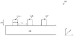
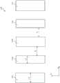
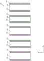
图1是在一个或多个实施例中的根据本发明各个方面构建的用于制造集成电路(IC)的方法20的流程图。图2-10是处于各个制造阶段的半导体结构100的截面图。半导体结构100是由方法20制造的半导体结构的一个实例。参考图1至图10共同描述方法20和半导体结构100。FIG. 1 is a flowchart of a method 20 for fabricating an integrated circuit (IC) constructed in accordance with various aspects of the present invention, in one or more embodiments. 2-10 are cross-sectional views of the
方法20开始于操作22,在衬底102上形成硬掩模图案104。硬掩模图案104是伪图案并且将会在后续的制造阶段去除。硬掩模图案104也称为心轴图案104。衬底102包括诸如硅晶圆的半导体衬底。可选地,衬底102包括锗、硅锗或其他适合的半导体材料。衬底102也可包括诸如n型阱和p型阱的多个掺杂区。在一个实施例中,衬底102包括外延(或epi)半导体层。在另一实施例中,衬底102包括通过适合的技术(诸如称为注氧隔离(SIMOX)的技术)形成的用于隔离的隐埋介电材料层。在一些实施例中,衬底102可以为诸如绝缘体上硅(SOI)的绝缘体上半导体。Method 20 begins at operation 22 , forming
在操作22中,设计者接收或提供IC布局(或IC设计图案)。在一个实例中,设计者可为与分配为根据IC布局制造IC产品的半导体制造商分离的设计公司或者设计团队。在多个实施例中,半导体制造商能够制造光掩模(掩模)、半导体晶圆或者这两者。IC布局包括设计用于IC产品并且基于IC产品的规格的多个几何图案。例如,IC布局包括限定鳍状有源区结构的图案,其中,多个诸如鳍状场效应晶体管(FinFET)的IC器件形成在鳍状有源区结构上。在一个实施例中,IC图案限定在光掩模(掩模)中。In operation 22, a designer receives or provides an IC layout (or IC design pattern). In one example, the designer may be a design house or design team separate from the semiconductor manufacturer assigned to manufacture IC products according to the IC layout. In various embodiments, a semiconductor manufacturer can manufacture photomasks (masks), semiconductor wafers, or both. The IC layout includes a plurality of geometric patterns designed for the IC product and based on the specifications of the IC product. For example, an IC layout includes a pattern defining a fin-shaped active area structure on which a plurality of IC devices, such as fin field effect transistors (FinFETs), are formed. In one embodiment, the IC pattern is defined in a photomask (mask).
在本实施例中,心轴图案104限定多个开口,从而使得衬底102在开口内露出。在一个实施例中,心轴图案104的形成包括沉积诸如介电材料(例如氧化硅、氮化硅)的心轴材料层;形成光刻胶图案;以及将光刻胶层用作蚀刻掩模来蚀刻心轴材料层,从而形成心轴图案104。光刻胶图案包括对辐射束敏感的光刻胶材料,并且由光刻工艺来形成。在一个实例中,光刻工艺包括在心轴材料层上涂布光刻胶层,根据IC布局对光刻胶层实施光刻曝光工艺,以及对所曝光的光刻胶层进行显影以形成光刻胶图案。光刻曝光工艺使用诸如光(诸如紫外光-UV、深紫外光-DUV或超紫外光-EUV)的辐射束以化学地改变光刻胶层的曝光的部分。在本实施例中,光刻曝光工艺利用了具有限定于其上的IC布局的掩模。该掩模可为二元掩模、相移掩模(phase shift mask,PSM)或反射掩模(诸如用于EUV光刻曝光工艺的反射掩模)。In this embodiment, the
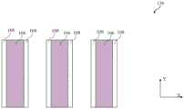
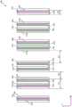
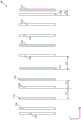
心轴图案104包括沿Y方向定向并且在垂直于Y方向的X方向上间隔开的多个第一部件。第一部件的实例也称作104,或者具体地分别称作104A、104B和104C。如图2中所示,第一部件104具有第一宽度L和第一间距S。特别地,第一宽度L可为常量或可选地为部件和部件之间变化的变量。类似地,第一间距S可为常量或可为在不同部件之间变化的变量。The
方法20进行至操作24,在心轴图案104的侧壁上形成第一间隔件图案106,如图3所示。在一个实施例中,第一间隔件图案106的形成包括在衬底102和心轴图案104上沉积第一间隔件材料层,然后对第一间隔件材料层实施第一各向异性蚀刻,从而形成第一间隔件图案106。第一间隔件材料层可包括诸如氧化硅、氮化硅或碳化硅但不同于心轴材料层的介电材料以获得在第一各向异性蚀刻期间的蚀刻选择性。第一间隔件材料层的沉积包括诸如化学汽相沉积(CVD)的适合的技术。第一间隔件材料层的厚度称作第一工艺参数“b”。在一个实例中,第一各向异性蚀刻可包括等离子体蚀刻。第一间隔件图案106包括沿Y方向定向并且在X方向上相互间隔开的多个第二部件。Method 20 proceeds to
方法20进行至操作26,去除心轴图案104,如图4所示。通过蚀刻工艺去除心轴图案104,该工艺选择性地去除心轴材料层但是基本上不蚀刻第一间隔件材料层。如图4中所示,第一间隔件图案106中的第二部件具有第二宽度,该第二宽度基本上等于第一间隔件材料层的沉积厚度“b”。Method 20 proceeds to
方法20进行至操作28,在第一间隔件图案106的侧壁上形成第二间隔件图案108,如图5所示。在一个实施例中,第二间隔件图案108的形成包括将第二间隔件材料层沉积在衬底102和第一间隔件图案106上,然后对第二间隔件材料层实施第二各向异性蚀刻,从而形成第二间隔件图案108。第二间隔件材料层可包括诸如氧化硅、氮化硅或碳化硅但不同于第一间隔件材料层的介电材料以获得在第二各向异性蚀刻期间的蚀刻选择性。第二间隔件材料层的沉积包括诸如CVD的适合的技术。第二间隔件材料层的厚度称作第二工艺参数“c”。在一个实例中,第二各向异性蚀刻可包括等离子体蚀刻。第二间隔件图案108包括沿Y方向定向并且在X方向上相互间隔开的多个第三部件。Method 20 proceeds to
方法20进行至操作30,去除第一间隔件图案106,如图6中所示。通过蚀刻工艺去除第一间隔件图案106,该工艺选择性地去除第一间隔件材料层但是基本上不蚀刻第二间隔件材料层。如图6所示,第二间隔件图案108中的第三部件具有第三宽度,该第三宽度基本上等于第二间隔件材料层的沉积厚度“c”。Method 20 proceeds to
方法20进行至操作32,形成具有开口112的切割图案110,使得开口112内的第三部件的子集未被覆盖,如图7所示。切割图案110在随后的蚀刻工艺期间用作蚀刻掩模以去除第二间隔件图案108中的第三部件的子集。切割图案110可包括由第二光刻工艺图案化的光刻胶层。第二光刻工艺可利用诸如浸没式光刻的适合的光刻技术。可选地,切割图案110包括不同于第二间隔件材料层的硬掩模材料(诸如氧化硅或氮化硅的介电材料)以获得蚀刻选择性,并且通过包括沉积介电材料层、在介电材料层上形成光刻胶图案以及将光刻胶图案用作蚀刻掩模来蚀刻介电材料层的工序图案化。切割图案110和限定于其上的多个开口112在图41中以俯视图进一步示出。Method 20 proceeds to
方法20进行至操作34,去除第二间隔件图案108中的第三部件的子集,如图8所示。通过蚀刻工艺去除第二间隔件图案108中的第三部件的子集,该蚀刻工艺选择性地去除第二间隔件材料层但是基本上不蚀刻切割图案110。如图9中所示,此后,通过适合的工艺去除切割图案110。在切割图案110是光刻胶图案的一个实例中,通过湿法剥离或等离子体灰化去除切割图案110。在切割图案110是介电材料的硬掩模图案的另一实例中,可通过湿蚀刻工艺去除切割图案110以选择性地去除硬掩模材料。第二间隔件图案仍标记为108但是由于去除了第三部件的子集,因而减少了第二间隔件图案。Method 20 proceeds to
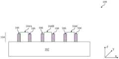
方法20进行至操作36,将第二间隔件图案108用作蚀刻掩模来蚀刻衬底102以在衬底102中形成多个沟槽114,参考图10。设计施加于衬底102的蚀刻工艺以选择性地蚀刻衬底102,诸如选择性地蚀刻硅。蚀刻工艺可包括干蚀刻和/或湿蚀刻并且可包括多个蚀刻步骤以优化蚀刻效果。例如,蚀刻工艺包括干蚀刻以基本上去除大部分以及湿蚀刻以进一步去除剩余部分。在一个实施例中,一个或多个硬掩模层设置在衬底102上。在此情况下,第二间隔件图案108用于图案化硬掩模层。此后,将衬底102图案化以形成穿过图案化的硬掩模层的沟槽114。Method 20 proceeds to
可选地,第二间隔件图案108用作离子注入掩模。对衬底施加离子注入工艺以穿过第二间隔件图案108的开口在衬底102中形成多种掺杂部件。第二间隔件图案108中的第三部件防止离子注入将掺杂剂引入由第三部件保护的区域中的衬底。Optionally, the
此后,通过诸如湿蚀刻的适合的蚀刻工艺去除第二间隔件图案108。方法20可包括在操作22-26之前,之间或之后的其他操作。例如,方法20包括操作38,在衬底102中形成IC图案。在本实施例中,第二间隔件图案108限定用于FinFET的鳍状有源区。在这种情况下,操作38在衬底102中形成鳍状有源区。Thereafter, the
在一个实施例中,操作38包括形成浅沟槽隔离(STI)部件和将STI部件开槽以形成鳍状有源区。STI部件的形成可实施包括以下步骤的工序:沉积一个或多个介电材料以填充沟槽;以及执行诸如化学机械抛光(CMP)的抛光工艺,以去除衬底上的过量的介电材料并且平坦化顶部表面。STI部件的开槽可包括蚀刻工艺以选择性地蚀刻STI部件,使得STI部件被开槽在衬底102的顶部表面之下。In one embodiment,
在另一实施例中,操作38包括形成STI部件以及在衬底102上选择性地外延生长半导体材料,从而形成鳍状有源区。选择性地外延生长在衬底102上的半导体材料可与衬底的半导体材料相同或可选地不同。例如,衬底102包括硅,并且选择性地外延生长于其上的半导体材料包括锗(Ge)、硅锗(SiGe)或诸如III-V族半导体材料的在组成上不同于硅的其他半导体材料。在另一实例中,衬底102包括锗或硅锗,并且选择性地外延生长于其上的半导体材料包括硅或在组成上不同的其他半导体材料。In another embodiment,
所公开的方法20形成具有不同结构的第二间隔件图案108(图6或图9中示出)。特别地,第二间隔件图案108可包括不规则图案。例如,第二间隔件图案具有非周期性结构。具体地,在不规则图案中,第二间隔件图案108中的第三部件具有在第三部件之间变化的可变节距。在方法200中,引入并定义了两组参数:第一组包括称作掩模参数的L和S,并且第二组包括称作工艺参数的b和c。掩模参数与用于方法20的光刻工艺的掩模相关。掩模参数还可包括与切割图案110相关的其他参数。工艺参数与诸如沉积以分别形成第一和第二间隔件材料层的各种工艺操作相关联。方法20还包括选择掩模参数和工艺参数的多种组合的步骤,以形成不同的IC图案,特别是不规则IC图案。下面根据各个实施例进一步描述。The disclosed method 20 forms the second spacer pattern 108 (shown in FIG. 6 or FIG. 9 ) having a different structure. In particular, the
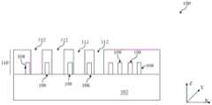
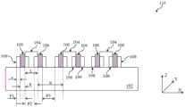
图11示出了半导体结构100的截面图,但是多个部件仅为更好的理解的目的而出现,虽然在现实中那些部件不会在相同的制造阶段出现,因此图11中的结构称作半导体结构116。可以理解,结构116仅用于说明的目的。图13示出了根据另一实施例的半导体结构134的截面图。结构134与结构116相似,其中多个部件仅为更好理解的目的而出现,虽然在现实中那些部件不会在相同的制造阶段出现。结构134还包括具有一个或多个切割开口112的切割图案。各个参数标记在图11和图13中以用于下面的描述。图12是在各个实施例中的根据本发明的各方面构建的用于制造IC图案的方法120的流程图。方法120用于确定多个参数并且与方法20结合以形成具有各种结构(特别是各种不规则结构)的IC图案。例如,执行方法120以确定掩模和工艺参数;并执行方法20以根据由方法120确定的参数来形成IC图案。参考图11至图13并进一步参考其他附图来描述方法120。FIG. 11 shows a cross-sectional view of a
方法120开始于操作122,接收具有多个第三部件的IC布局,第三部件是诸如图9中的、可在衬底102中限定多个鳍状有源区的第二间隔件图案108。Method 120 begins at
方法120可进行至操作124,确定第三部件(也称作108)中的一些节距。第三部件沿Y方向定向并且在X方向上相互分隔开。在一个实施例中,第三部件108在X方向上以具有一个节距P1的周期性结构配置。将节距定义为从第二间隔件图案中的一个部件的边缘到第二间隔件图案中的邻近部件的相同边缘的尺寸。在另一实施例中,第三部件108在X方向上以具有两个节距P1和P2或可选地具有诸如P1、P2和P3的多个节距的非周期性结构(不规则结构)配置。在不规则结构中,第三部件的第一子集具有一个节距(诸如P1)并且第三部件的第二子集具有另一节距(诸如P2)等。Method 120 may proceed to
方法120进行至操作126,确定第三部件108中的每个节距的相应值。那些值可直接从IC布局中提取。例如,P1是82nm,以及P2是94nm。Method 120 proceeds to
方法120进行至操作128,基于IC布局,特别是基于节距的相应值,来确定各个掩模参数和工艺参数。掩模参数包括限定在掩模中以在方法20的第一光刻工艺中形成心轴图案104的L和S。工艺参数包括用于方法20以分别沉积第一和第二间隔件材料层的b和c。那些参数在图11中标出。随后根据各个实例进一步描述确定那些参数的方法。在一个实例中,如图11所示,第一节距P1=b+c、第二节距P2=L-c,以及第三节距P3=S-2b-c。然而,通过穿过切割图案110的开口112的蚀刻去除心轴图案104的两个邻近第一部件之间的间隙内的第二间隔件图案108的第三部件的情况下,第三节距P3=S+c。基于那些等式,可基于节距P1、P2和P3来确定参数L、S、b和c。Method 120 proceeds to
在一种情况下,在确定参数期间可有更多的自由性。在这种情况下,可根据诸如掩模检查规则和制造能力的其他考虑进一步调整该参数。In one case, there may be more freedom during the determination of the parameters. In this case, this parameter can be further tuned based on other considerations such as mask inspection rules and manufacturing capabilities.
在其他情况下,可能没有足够自由度来选择适合的参数。例如在有四个或更多节距的情况下,恰当地设计切割图案110以在方法20中的第二光刻工艺期间获得不规则图案,从而形成切割图案110。如图13所示,切割图案包括限定要去除的多个第三部件的一个或多个开口112。为此目的,切割图案可设计为具有不同的宽度、间距、一个或多个节距。另外或可选地,工艺参数b和/或c可设计成引起合并以获得具有多个节距的不规则图案。切割图案可设计为去除合并的部件。In other cases, there may not be enough degrees of freedom to choose suitable parameters. Cutting
在节距数目为2的另一实例中,可通过要求P1=P2、P2=P3或P1=P3来形成不规则图案。在节距数目为1的又一实例中,可通过要求P1=P2=P3来形成不规则图案。In another example where the number of pitches is 2, the irregular pattern can be formed by requiring P1=P2, P2=P3 or P1=P3. In yet another example where the number of pitches is 1, an irregular pattern can be formed by requiring P1 = P2 = P3.
在另一实例中,通过调整L和S从而使得S<=2b并且|L-S|=2c,第一间隔件图案106中的第二部件合并,并且得到具有节距P1=(L+S)/2的周期(规则)图案。在一个特定实例中,b=24、c=12、S=48并且L=72,因此P1=60。那些值可为诸如纳米(nm)的任何合适的单位。In another example, by adjusting L and S such that S<=2b and |L−S|=2c, the second features in the
在另一实例中,通过调整L和S从而使得S<=2b+2c并且将“D”设定为在方法20的操作32和34期间要去除的伪部件(如图13中所示),获得了具有一个节距为L-c并且另一节距为S+c的非周期(不规则)图案。在一个特定实例中,c=12、S=72并且L=80,因此一个节距为58并且另一节距为84。出于诸如优化工艺窗口的其他考虑,参数b具有可调整的自由度。In another example, by adjusting L and S such that S<=2b+2c and setting "D" as the dummy component to be removed during
方法120进行至操作130,根据IC图案和所确定的掩模参数来制造掩模。操作130可包括根据所确定的掩模参数来产生心轴图案并且制造限定心轴图案的掩模。操作130还可包括根据所确定的掩模参数产生切割图案并且制造限定切割图案的掩模。掩模可为二元掩模、相移掩模、反射掩模或其他适合的掩模。Method 120 proceeds to
方法120进行至操作132,在相应的光刻工艺期间基于所确定的工艺参数并使用掩模来制造晶圆。在本实施例中,操作132包括方法20。例如,操作132包括使用根据掩模参数L和S设计的掩模通过第一光刻工艺来形成心轴图案104;通过包括根据所确定的工艺参数b沉积具有第一厚度的第一间隔件材料层的工序来形成第一间隔件图案106;以及通过包括根据所确定的工艺参数c沉积具有第二厚度的第二间隔件材料层的工序来形成第二间隔件图案108。Method 120 proceeds to
操作132还可包括通过使用根据与切割图案相关联的掩模参数(诸如切割图案中的切割部件的相应宽度和间隔)设计的掩模的第二光刻工艺来形成切割图案110。
下面根据各个实施例来描述方法20和120的其他实施例。图14至图17是根据一个实施例所构建的处于各个制造阶段的半导体结构136的俯视图。通过方法120根据所接收的IC布局来确定各个掩模参数和工艺参数并且通过方法20来实现半导体结构136的制造。Other embodiments of methods 20 and 120 are described below according to various embodiments. 14-17 are top views of a
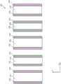
参考图14,心轴图案104形成在衬底102上。为了简明,衬底102在下面的附图中不再示出。心轴图案104包括周期结构中的具有第一宽度L和第一间距S的多个第一部件。在本实施例中,比率L/S等于3/2或1.5。在用于说明的一个实例中,宽度L约为72nm并且间距S约为48nm。心轴图案104通过诸如方法20的操作22的工序来形成。Referring to FIG. 14 , a
参考图15,第一间隔件图案106通过诸如方法20的操作24的适合工序形成在心轴图案104的侧壁上。特别地,第一间隔件图案106的第二部件在心轴图案104的第一部件之间的间隙内合并在一起。在这种情况下,第一间隔件材料层的沉积厚度b等于第一间距S的一半,用公式表示为b=S/2。在上述实例中,沉积厚度b约为24nm。Referring to FIG. 15 , a
参考图16,心轴图案104通过诸如方法20的操作26的工序去除,以及第二间隔件图案108通过诸如方法20的操作28的适合工序形成在第一间隔件图案106的侧壁上。特别地,第二间隔件材料层的沉积厚度c等于第一厚度b的一半,用公式表示为c=b/2。在上述实例中,沉积厚度c约为12nm。Referring to FIG. 16 , the
参考图17,第一间隔件图案106通过诸如方法20的操作30的工序去除,从而形成了具有节距P=S+c或P=(L+S)/2的周期结构(规则结构)的第二间隔件图案108。在上述实例中,第二间隔件图案108的节距约为60nm。Referring to FIG. 17, the
更通常地,对于结构136,调整那些参数使得S<=2b以及|L-S|=2c,第二间隔件图案108的周期结构具有节距P=(L+S)/2。More generally, those parameters are adjusted such that S<=2b and |L−S|=2c for the
图18-22是根据另一实施例构建的处于各个制造阶段的半导体结构138的俯视图。通过方法120根据所接收的IC布局来确定各个掩模参数和工艺参数,并且通过方法20来实现半导体结构138的制造。18-22 are top views of a
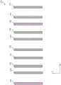
参考图18,心轴图案104形成在衬底102上。为了简明,未示出衬底102。心轴图案104包括周期结构中的具有第一宽度L和第一间距S的多个第一部件。在本实施例中,比率L/S等于1/2或0.5。在用于示例说明的一个实例中,宽度L为约48nm并且间距S为约96nm。心轴图案104通过诸如方法20的操作22的工序来形成。Referring to FIG. 18 , a
参考图19,第一间隔件图案106通过诸如方法20的操作24的适合的工序形成在心轴图案104的侧壁上。特别地,第一间隔件材料层的沉积厚度b等于第一宽度L的一半,用公式表示为b=L/2。在上述实例中,沉积厚度b为约24nm。Referring to FIG. 19 , a
参考图20,通过诸如方法20的操作26的工序去除心轴图案104。Referring to FIG. 20 , the
参考图21,第二间隔件图案108通过诸如方法20的操作28的适合工序形成在第一间隔件图案106的侧壁上。特别地,第二间隔件材料层的沉积厚度c等于第一厚度b的一半,用公式表示为c=b/2。在上述实例中,沉积厚度c为约12nm。Referring to FIG. 21 ,
参考图22,第一间隔件图案106由诸如方法20的操作30的工序去除,从而形成了具有节距P=b+c或P=(L+S)/4的周期结构(规则结构)的第二间隔件图案108。在上述实例中,第二间隔件图案108的节距为约36nm。Referring to FIG. 22, the
图23-29是根据另一实施例构建的处于各个制造阶段的半导体结构140的俯视图。通过方法120根据所接收的IC布局来确定各个掩模参数和工艺参数,并且通过方法20来实现半导体结构140的制造。23-29 are top views of a
参考图23,心轴图案104形成在衬底102上。为了简明,未示出衬底102。心轴图案104包括非周期结构中的具有第一间距S的多个第一部件。然而,如图23所示,第一部件包括具有一个宽度L1的第一子集以及具有另一宽度L2的第二子集。L1大于L2。在本实施例中,比率(L1-L2)/(L2-S)等于1/2或0.5。在用于说明的一个实例中,宽度L1为约106nm,L2为约94nm并且间距S为约70nm。心轴图案104通过诸如方法20的操作22的工序来形成。Referring to FIG. 23 , a
参考图24,第一间隔件图案106通过诸如方法20的操作24的适合的工序形成在心轴图案104的侧壁上。在本实例中,第一间隔件材料层的沉积厚度b等于L2-S。在上述实例中,沉积厚度b为约24nm。Referring to FIG. 24 , a
参考图25,心轴图案104通过诸如方法20的操作26的工序去除。Referring to FIG. 25 , the
参考图26,第二间隔件图案108通过诸如方法20的操作28的适合的工序形成在第一间隔件图案106的侧壁上。特别地,第二间隔件材料层的沉积厚度c等于第一厚度b的一半,用公式表示为c=b/2。在这种情况下,如图26所示,第二间隔件图案108中的一些第三部件合并在一起。在上述实例中,沉积厚度c为约12nm。第二间隔件图案108具有多个节距,诸如图26中分别地示出的节距P1、P2、P3和P4。具体地,P1=S+c、P2=L2-c、P3=L1-c和P4=b+c。由于合并的第三部件将在随后的操作中去除,因而在限定多个节距中不考虑合并的第三部件。在上述实例中,P1=70nm+12nm=82nm;P2=94nm-12nm=82nm;P3=106nm-12nm=94nm;以及P4=24nm+12nm=36nm.Referring to FIG. 26 ,
参考图27,第一间隔件图案106通过诸如方法20的操作30的工序去除。Referring to FIG. 27 , the
参考图28,切割图案110通过诸如方法20的操作32的工序形成在衬底102和第二间隔件图案108上。切割图案110包括限定了第二间隔件图案108的要去除的部分的多个开口112。在本实施例中,开口112与所合并的第三部件对准。Referring to FIG. 28 , a
参考图29,切割图案110的开口112内的第二间隔件图案108的部分由诸如方法20的操作34的工序去除,从而形成具有多个节距的不规则结构的第二间隔件图案108的最终结构。Referring to FIG. 29 , portions of the
图30-36是根据另一实施例构建的处于各个制造阶段的半导体结构142的俯视图。通过方法120根据所接收的IC布局来确定各个掩模参数和工艺参数并且通过方法20来实现半导体结构142的制造。30-36 are top views of a
参考图30,心轴图案104形成在衬底102上。心轴图案104包括在周期结构中的具有宽度L和间距S的多个第一部件。Referring to FIG. 30 , a
参考图31,第一间隔件图案106通过诸如方法20的操作24的适合的工序形成在心轴图案104的侧壁上。Referring to FIG. 31 , a
参考图32,心轴图案104由诸如方法20的操作26的工序去除。Referring to FIG. 32 , the
参考图33,第二间隔件图案108通过诸如方法20的操作28的适合的工序形成在第一间隔件图案106的侧壁上。Referring to FIG. 33 ,
参考图34,第一间隔件图案106由诸如方法20的操作30的工序去除。Referring to FIG. 34 , the
参考图35,切割图案110通过诸如方法20的操作32的工序形成在衬底102和第二间隔件图案108上。切割图案110包括限定了要去除的第二间隔件图案108的部分的多个开口112。在本实施例中,切割图案110具有带有相应的宽度和间隔的多个开口的不规则结构。如图35中所示,开口112A具有第一宽度,从而使得第二间隔件图案108仅有一个部件在其内露出。开口112B具有第二宽度,从而使得第二间隔件图案108的两个部件在其内露出。开口112C具有第三宽度,从而使得第二间隔件图案108的三个部件在其内露出。切割图案110可具有不同尺寸的其他开口。此外,邻近的开口之间的距离在不同的位置可以变化。例如,第二开口112B和第三开口112C之间的间距不同于第三开口112C和第四开口112D之间的间距。Referring to FIG. 35 , a
参考图36,切割图案110的开口112内的第二间隔件图案108的部分由诸如方法20的操作34的工序去除,从而形成具有多个节距的不规则结构的第二间隔件图案108的最终结构。Referring to FIG. 36 , portions of the
图37-38是根据另一实施例构建的处于各个制造阶段的半导体结构114的俯视图。通过方法120根据所接收的IC布局来确定各个掩模参数和工艺参数并且通过方法20来实现半导体结构144的制造。37-38 are top views of a
形成半导体结构144的工序类似于形成半导体结构142的工序,其中不规则切割图案110用于获得具有多个节距和配置的第二间隔件图案108的最终结构。此外,如图37所示,半导体结构144中的心轴图案104进一步限定为另一不规则结构。例如,图37中的心轴图案104包括彼此不同的诸如L1、L2和L3的多个宽度。The process of forming the
心轴图案104由心轴掩模所限定,并且由第一光刻工艺形成。切割图案110由切割掩模所限定,并且由第二光刻工艺形成。如图38所示,通过结合心轴掩模中的第一不规则图案和切割掩模中的第二不规则图案,第二间隔件图案108的更为复杂的结构形成在衬底102上。因此,所述方法提供了更大的自由度以调整第二间隔件图案108的最终结构。The
图39是用于制造IC图案的方法150的流程图。此外,方法150用于确定多种参数并且与方法20相结合以形成具有多种结构(特别是多种不规则结构)的IC图案。例如,执行方法150以确定掩模和工艺参数;并且根据由方法150所确定的参数执行方法20以形成IC图案。方法150可为方法120的一个实例。参考图39、图11和其他附图来描述方法150。FIG. 39 is a flowchart of a
方法150开始于操作152,接收具有多个第三部件的IC布局,诸如图9中的可限定衬底102中多个鳍状有源区的第二间隔件图案108。在本实施例中,IC布局具有两个节距P1和P2。
方法150可进行至操作154,确定第三部件108中的节距的相应值。那些值可从IC布局直接提取。在本实例中,确定节距P1和P2。
方法150进行至操作156,基于IC布局特别是基于相应的节距P1和P2来确定掩模参数L和工艺参数c。在本实例中,如图11所示,第一节距P1=b+c并且第二节距P2=L-c。基于公式P2=L-c,确定参数L和c。
方法150进行至操作158,基于IC布局特别是基于相应的节距P1确定工艺参数b。在本实例中,基于第一节距P1=b+c,确定参数b。The
方法150进行至操作160,基于IC布局特别是基于空间关系S=L-2c(意味着要求第三节距P3=P2)确定掩模参数S。如图11所示,由于P2=L-c并且P3=S+c,P2=P3给出了S=L-2c的条件。基于公式S=L-2c,确定参数S。
方法150进行至操作162,根据IC图案和所确定的包括L和S的掩模参数来制造掩模。操作162可包括根据所确定的掩模参数产生心轴图案并制造限定心轴图案的掩模。操作162还可包括根据所确定的掩模参数产生切割图案并制造限定切割图案的掩模。掩模可为二元掩模、相移掩模、反射掩模或其他适合的掩模。
方法150可进行至操作164,基于所确定的工艺参数且在相应的光刻工艺期间使用掩模来制造晶圆。在本实施例中,操作164包括方法20。例如,操作164包括使用根据掩模参数L和S设计的掩模通过第一光刻工艺来形成心轴图案104;通过包括根据所确定的工艺参数b来沉积具有第一厚度的第一间隔件材料层的工序来形成第一间隔件图案106;以及通过根据所确定的工艺参数c沉积具有第二厚度的第二间隔件材料层的工序来形成第二间隔件图案108。
操作164还可包括通过使用根据与切割图案相关联的掩模参数(诸如切割图案中的切割部件的相应宽度和间隔)设计的掩模的第二光刻工艺来形成切割图案110。
图40是用于制造IC图案的方法170的流程图。此外,方法170用于确定多种参数并且与方法20相结合以形成具有多种结构(特别是多种不规则结构)的IC图案。例如,执行方法170以确定掩模和工艺参数;并且根据由方法170所确定的参数执行方法20以形成IC图案。方法170可为方法120的一个实例。参考图40、图11和其他附图来描述方法170。FIG. 40 is a flowchart of a
方法170开始于操作172,接收具有多个第三部件的IC布局,第三部件为诸如图9中的可在衬底102中限定多个鳍状有源区的第二间隔件图案108。在本实施例中,IC布局具有节距P1、P2和P3。
方法170可进行至操作174,确定第三部件108中的节距的相应值。那些值可从IC布局直接提取。在本实例中,确定节距P1、P2和P3。
方法170进行至操作176,基于IC布局特别是基于相应的节距P1和P2来确定掩模参数L和工艺参数c。在本实例中,第一节距P1=b+c,第二节距P2=L-c以及第三节距P3=S+c(假定在心轴图案104的两个邻近的第一部件之间的间隙内的第二间隔件图案108的第三部件通过穿过切割图案110的开口112的蚀刻被去除)。否则,如图11所示,P3=S-2b-c。基于公式P2=L-c,确定参数L和c。
方法170进行至操作178,基于IC布局特别是基于相应的节距P1确定工艺参数b。在本实例中,基于第一节距P1=b+c,确定参数b。The
方法170进行至操作180,基于IC布局特别是基于相应的节距P3确定掩模参数S。在本实例中,基于第三节距P3=S+c,确定参数S。否则,如果切割图案110不被应用于去除心轴图案104的邻近的第三部件之间的间隙内的第三部件,基于公式P3=S-2b-c来确定参数S。
方法170进行至操作182,根据IC图案和所确定的包括L和S的掩模参数来制造掩模。操作182可包括根据所确定的掩模参数并制造限定心轴图案的掩模产生心轴图案。操作182还可包括根据所确定的掩模参数并制造限定切割图案的掩模产生切割图案。掩模可为二元掩模、相移掩模、反射掩模或其他适合的掩模。
方法170进行至操作184,基于所确定的工艺参数并且在相应的光刻工艺期间使用掩模来制造晶圆。在本实施例中,操作184包括方法20。例如,操作184包括使用根据掩模参数L和S设计的掩模通过第一光刻工艺来形成心轴图案104;通过包括根据所确定的工艺参数b来沉积具有第一厚度的第一间隔件材料层的工序来形成第一间隔件图案106;以及通过包括根据所确定的工艺参数c来沉积具有第二厚度的第二间隔件材料层的工序来形成第二间隔件图案108。
操作184还可包括通过使用根据与切割图案相关的掩模参数(诸如切割图案中的切割部件的相应宽度和间隔)设计的掩模的第二光刻工艺来形成切割图案110。
通过使用所公开的方法,由方法20通过调节各个掩模和工艺参数来形成复杂的IC图案,各个掩模和工艺参数是由方法120进一步获得的。特别地,所公开的方法能够形成具有多个节距的非周期(不规则)结构的图案。其他优势可出现在不同的实施例中。例如,通过实施所公开的方法,可以通过更少的制造步骤和/或更低的分辨率的光刻系统来形成复杂的结构,因此减少了制造成本。可在不背离本发明的精神的情况下实施其他实施例和变形例。在一个实施例中,通过公开的方法不是形成鳍状有源区而是形成诸如用于场效应晶体管的多个栅电极或者用于互连结构的金属线的其他IC部件。Using the disclosed method, complex IC patterns are formed by method 20 by adjusting various mask and process parameters, which are further obtained by method 120 . In particular, the disclosed methods are capable of forming patterns of aperiodic (irregular) structures with multiple pitches. Other advantages may arise in different embodiments. For example, by implementing the disclosed methods, complex structures may be formed with fewer fabrication steps and/or lower resolution photolithography systems, thereby reducing fabrication costs. Other embodiments and modifications can be implemented without departing from the spirit of the invention. In one embodiment, instead of fin-shaped active regions, other IC components such as multiple gate electrodes for field effect transistors or metal lines for interconnect structures are formed by the disclosed method.
因此,本发明提供了集成电路(IC)设计方法。方法包括通过第一光刻工艺在衬底上形成心轴图案;在心轴图案的侧壁上形成第一间隔件图案;去除心轴图案;在第一间隔件图案的侧壁上形成第二间隔件图案;去除第一间隔件图案;以及将第二间隔件图案用作蚀刻掩模来蚀刻衬底。Accordingly, the present invention provides integrated circuit (IC) design methods. The method includes forming a mandrel pattern on a substrate through a first photolithography process; forming a first spacer pattern on a sidewall of the mandrel pattern; removing the mandrel pattern; forming a second spacer on a sidewall of the first spacer pattern removing the first spacer pattern; and etching the substrate using the second spacer pattern as an etching mask.
本发明还提供了用于集成电路(IC)的方法的另一实施例。该方法包括接收具有多个部件的IC布局;确定多个部件中的节距;基于部件中的节距确定掩模参数和工艺参数;以及根据掩模参数制造掩模。The present invention also provides another embodiment of a method for an integrated circuit (IC). The method includes receiving an IC layout having a plurality of features; determining pitches in the plurality of features; determining mask parameters and process parameters based on the pitches in the features; and fabricating a mask based on the mask parameters.
本发明还提供了用于集成电路(IC)的方法的另一实施例。该方法包括接收具有多个部件的IC布局,其中所述多个部件具有相互不同的第一节距P1和第二节距P2;根据P2=L-c确定第一工艺参数c,其中L是部件的第一宽度;以及根据P1=b+c确定第二工艺参数b。The present invention also provides another embodiment of a method for an integrated circuit (IC). The method includes receiving an IC layout having a plurality of components, wherein the plurality of components have mutually different first pitch P1 and second pitch P2; determining a first process parameter c according to P2=L-c, where L is a pitch of the component the first width; and determining the second process parameter b according to P1=b+c.
上面概述了若干实施例的特征从而使得本领域技术人员可以更好地理解下面的详细描述。本领域技术人员应该理解,可以很容易地使用本发明作为基础来设计或更改其他用于达到与这里所介绍实施例相同的目的和/或获得相同优点的工艺和结构。本领域技术人员也应该意识到,这样的等效构造并不背离本发明的精神和范围,并且在不背离本发明的精神和范围的情况下,可以作出各种变化、替换以及改变。The foregoing outlines features of several embodiments so that those skilled in the art may better understand the detailed description that follows. Those skilled in the art should understand that the present invention can be easily used as a basis to design or modify other processes and structures for achieving the same purpose and/or obtaining the same advantages as the embodiments presented here. Those skilled in the art should also realize that such equivalent constructions do not depart from the spirit and scope of the invention, and that they could make various changes, substitutions and alterations herein without departing from the spirit and scope of the invention.
Claims (20)
Priority Applications (1)
| Application Number | Priority Date | Filing Date | Title |
|---|---|---|---|
| CN202010259126.6ACN111403277B (en) | 2013-08-20 | 2013-11-22 | Integrated circuit layout and method with double patterning |
Applications Claiming Priority (4)
| Application Number | Priority Date | Filing Date | Title |
|---|---|---|---|
| US13/971,363US8987008B2 (en) | 2013-08-20 | 2013-08-20 | Integrated circuit layout and method with double patterning |
| US13/971,363 | 2013-08-20 | ||
| CN201310601880.3ACN104425214A (en) | 2013-08-20 | 2013-11-22 | Integrated circuit layout and method with double patterning |
| CN202010259126.6ACN111403277B (en) | 2013-08-20 | 2013-11-22 | Integrated circuit layout and method with double patterning |
Related Parent Applications (1)
| Application Number | Title | Priority Date | Filing Date |
|---|---|---|---|
| CN201310601880.3ADivisionCN104425214A (en) | 2013-08-20 | 2013-11-22 | Integrated circuit layout and method with double patterning |
Publications (2)
| Publication Number | Publication Date |
|---|---|
| CN111403277A CN111403277A (en) | 2020-07-10 |
| CN111403277Btrue CN111403277B (en) | 2023-05-23 |
Family
ID=52480722
Family Applications (2)
| Application Number | Title | Priority Date | Filing Date |
|---|---|---|---|
| CN202010259126.6AActiveCN111403277B (en) | 2013-08-20 | 2013-11-22 | Integrated circuit layout and method with double patterning |
| CN201310601880.3APendingCN104425214A (en) | 2013-08-20 | 2013-11-22 | Integrated circuit layout and method with double patterning |
Family Applications After (1)
| Application Number | Title | Priority Date | Filing Date |
|---|---|---|---|
| CN201310601880.3APendingCN104425214A (en) | 2013-08-20 | 2013-11-22 | Integrated circuit layout and method with double patterning |
Country Status (2)
| Country | Link |
|---|---|
| US (1) | US8987008B2 (en) |
| CN (2) | CN111403277B (en) |
Families Citing this family (24)
| Publication number | Priority date | Publication date | Assignee | Title |
|---|---|---|---|---|
| US9711368B2 (en)* | 2013-04-15 | 2017-07-18 | United Microelectronics Corp. | Sidewall image transfer process |
| US9274413B2 (en)* | 2013-09-11 | 2016-03-01 | United Microelectronics Corp. | Method for forming layout pattern |
| US9401310B2 (en)* | 2014-02-03 | 2016-07-26 | Applied Materials, Inc. | Method to form trench structure for replacement channel growth |
| TWI557784B (en)* | 2014-09-18 | 2016-11-11 | 聯華電子股份有限公司 | Method for manufacturing fin field effect transistor |
| WO2016093087A1 (en)* | 2014-12-09 | 2016-06-16 | 東京エレクトロン株式会社 | Pattern forming method, gas cluster ion beam irradiation system and pattern forming apparatus |
| TWI697796B (en)* | 2015-04-10 | 2020-07-01 | 聯華電子股份有限公司 | Layout resetting method for modified layout processing |
| KR102403736B1 (en) | 2015-11-02 | 2022-05-30 | 삼성전자주식회사 | Semiconductor device and method of manufacturing the same |
| TWI677923B (en)* | 2015-11-10 | 2019-11-21 | 聯華電子股份有限公司 | Semiconductor device and method for fabricating the same |
| US9472464B1 (en)* | 2016-03-04 | 2016-10-18 | Globalfoundries Inc. | Methods to utilize merged spacers for use in fin generation in tapered IC devices |
| US10056265B2 (en)* | 2016-03-18 | 2018-08-21 | Taiwan Semiconductor Manufacturing Co., Ltd. | Directed self-assembly process with size-restricted guiding patterns |
| US9911606B2 (en)* | 2016-04-28 | 2018-03-06 | Taiwan Semiconductor Manufacturing Co., Ltd. | Mandrel spacer patterning in multi-pitch integrated circuit manufacturing |
| US9779944B1 (en)* | 2016-09-13 | 2017-10-03 | International Business Machines Corporation | Method and structure for cut material selection |
| US9818640B1 (en)* | 2016-09-21 | 2017-11-14 | Globalfoundries Inc. | Apparatus and method of forming self-aligned cuts in a non-mandrel line of an array of metal lines |
| US9818613B1 (en)* | 2016-10-18 | 2017-11-14 | Taiwan Semiconductor Manufacturing Company, Ltd. | Self-aligned double spacer patterning process |
| TWI604569B (en)* | 2016-11-15 | 2017-11-01 | 新唐科技股份有限公司 | Semiconductor device and method of forming same |
| US10418252B2 (en) | 2016-12-16 | 2019-09-17 | Taiwan Semiconductor Manufacturing Co, Ltd. | Fin-like field effect transistor patterning methods for increasing process margins |
| CN109216163A (en)* | 2017-06-29 | 2019-01-15 | 中芯国际集成电路制造(上海)有限公司 | The manufacturing method of semiconductor devices |
| US10276374B2 (en) | 2017-09-20 | 2019-04-30 | Globalfoundries Inc. | Methods for forming fins |
| CN109558025B (en)* | 2017-09-27 | 2024-04-02 | 京东方科技集团股份有限公司 | Touch panel, manufacturing method thereof and display device |
| US10991584B2 (en)* | 2017-12-19 | 2021-04-27 | International Business Machines Corporation | Methods and structures for cutting lines or spaces in a tight pitch structure |
| US11127594B2 (en)* | 2017-12-19 | 2021-09-21 | Tokyo Electron Limited | Manufacturing methods for mandrel pull from spacers for multi-color patterning |
| US10818505B2 (en)* | 2018-08-15 | 2020-10-27 | Taiwan Semiconductor Manufacturing Co., Ltd. | Self-aligned double patterning process and semiconductor structure formed using thereof |
| CN113451123B (en)* | 2020-03-24 | 2025-06-17 | 中芯国际集成电路制造(上海)有限公司 | Semiconductor structure and method for forming the same |
| CN116741626A (en)* | 2022-03-04 | 2023-09-12 | 长鑫存储技术有限公司 | Preparation method of semiconductor structure and semiconductor structure |
Citations (2)
| Publication number | Priority date | Publication date | Assignee | Title |
|---|---|---|---|---|
| CN101490807A (en)* | 2006-07-10 | 2009-07-22 | 美光科技公司 | Pitch reduction techniques using alternating spacer deposition during formation of semiconductor devices and systems including semiconductor devices |
| CN101512726A (en)* | 2006-09-14 | 2009-08-19 | 美光科技公司 | Efficient pitch doubling process |
Family Cites Families (8)
| Publication number | Priority date | Publication date | Assignee | Title |
|---|---|---|---|---|
| US6875703B1 (en)* | 2004-01-20 | 2005-04-05 | International Business Machines Corporation | Method for forming quadruple density sidewall image transfer (SIT) structures |
| US7345370B2 (en)* | 2005-01-12 | 2008-03-18 | International Business Machines Corporation | Wiring patterns formed by selective metal plating |
| US7776744B2 (en)* | 2005-09-01 | 2010-08-17 | Micron Technology, Inc. | Pitch multiplication spacers and methods of forming the same |
| US7488685B2 (en)* | 2006-04-25 | 2009-02-10 | Micron Technology, Inc. | Process for improving critical dimension uniformity of integrated circuit arrays |
| US7862962B2 (en) | 2009-01-20 | 2011-01-04 | Taiwan Semiconductor Manufacturing Company, Ltd. | Integrated circuit layout design |
| US8324036B2 (en)* | 2009-11-09 | 2012-12-04 | International Business Machines Corporation | Device having and method for forming fins with multiple widths for an integrated circuit |
| US8513131B2 (en)* | 2011-03-17 | 2013-08-20 | International Business Machines Corporation | Fin field effect transistor with variable channel thickness for threshold voltage tuning |
| KR101671082B1 (en)* | 2011-12-29 | 2016-10-31 | 인텔 코포레이션 | Spacer assisted pitch division lithography |
- 2013
- 2013-08-20USUS13/971,363patent/US8987008B2/enactiveActive
- 2013-11-22CNCN202010259126.6Apatent/CN111403277B/enactiveActive
- 2013-11-22CNCN201310601880.3Apatent/CN104425214A/enactivePending
Patent Citations (2)
| Publication number | Priority date | Publication date | Assignee | Title |
|---|---|---|---|---|
| CN101490807A (en)* | 2006-07-10 | 2009-07-22 | 美光科技公司 | Pitch reduction techniques using alternating spacer deposition during formation of semiconductor devices and systems including semiconductor devices |
| CN101512726A (en)* | 2006-09-14 | 2009-08-19 | 美光科技公司 | Efficient pitch doubling process |
Also Published As
| Publication number | Publication date |
|---|---|
| CN104425214A (en) | 2015-03-18 |
| US20150056724A1 (en) | 2015-02-26 |
| CN111403277A (en) | 2020-07-10 |
| US8987008B2 (en) | 2015-03-24 |
Similar Documents
| Publication | Publication Date | Title |
|---|---|---|
| CN111403277B (en) | Integrated circuit layout and method with double patterning | |
| CN103247574B (en) | The cutting mask pattern metallization processes of fin formula field effect transistor (FINFET) device | |
| CN102969353B (en) | Many fin devices and its manufacture method | |
| US10049885B2 (en) | Method for patterning a plurality of features for fin-like field-effect transistor (FinFET) devices | |
| US9589848B2 (en) | FinFET structures having silicon germanium and silicon channels | |
| US8603893B1 (en) | Methods for fabricating FinFET integrated circuits on bulk semiconductor substrates | |
| CN103247575B (en) | The Patternized technique of fin formula field effect transistor (FinFET) device | |
| US9236269B2 (en) | Field effect transistor (FinFET) device with a planar block area to enable variable Fin pitch and width | |
| US9318334B2 (en) | Method for fabricating semiconductor device | |
| US9634000B2 (en) | Partially isolated fin-shaped field effect transistors | |
| TWI705502B (en) | Finfet device and method for manufacturing the same | |
| KR20110011558A (en) | How to double your pattern density | |
| US9214356B2 (en) | Mechanisms for forming patterns | |
| US20150380261A1 (en) | Mechanisms for Forming Patterns Using Multiple Lithography Processes | |
| US20150014772A1 (en) | Patterning fins and planar areas in silicon | |
| CN109119470B (en) | Boundary spacer structures and integration | |
| US20190378717A1 (en) | Integration of device regions | |
| CN105789049A (en) | Method for patterning a plurality of features for fin-like field-effect transistor (finfet) devices | |
| CN110783175B (en) | Manufacturing method of embedded germanium-silicon, CMOS (complementary Metal oxide semiconductor) device and germanium-silicon growth region layout | |
| KR20090076130A (en) | Semiconductor device and manufacturing method thereof | |
| CN104934480B (en) | Fin formula field effect transistor structure and preparation method thereof | |
| US9553026B1 (en) | Semiconductor device and method for fabricating the same |
Legal Events
| Date | Code | Title | Description |
|---|---|---|---|
| PB01 | Publication | ||
| PB01 | Publication | ||
| SE01 | Entry into force of request for substantive examination | ||
| SE01 | Entry into force of request for substantive examination | ||
| GR01 | Patent grant | ||
| GR01 | Patent grant |