CN111402945A - Integrated circuit chip and die testing without cell arrays - Google Patents
Integrated circuit chip and die testing without cell arraysDownload PDFInfo
- Publication number
- CN111402945A CN111402945ACN201911251874.3ACN201911251874ACN111402945ACN 111402945 ACN111402945 ACN 111402945ACN 201911251874 ACN201911251874 ACN 201911251874ACN 111402945 ACN111402945 ACN 111402945A
- Authority
- CN
- China
- Prior art keywords
- signal
- integrated circuit
- data
- circuit chip
- selection signal
- Prior art date
- Legal status (The legal status is an assumption and is not a legal conclusion. Google has not performed a legal analysis and makes no representation as to the accuracy of the status listed.)
- Granted
Links
Images


Classifications
- G—PHYSICS
- G11—INFORMATION STORAGE
- G11C—STATIC STORES
- G11C29/00—Checking stores for correct operation ; Subsequent repair; Testing stores during standby or offline operation
- G11C29/006—Checking stores for correct operation ; Subsequent repair; Testing stores during standby or offline operation at wafer scale level, i.e. wafer scale integration [WSI]
- G—PHYSICS
- G11—INFORMATION STORAGE
- G11C—STATIC STORES
- G11C29/00—Checking stores for correct operation ; Subsequent repair; Testing stores during standby or offline operation
- G11C29/04—Detection or location of defective memory elements, e.g. cell constructio details, timing of test signals
- G11C29/08—Functional testing, e.g. testing during refresh, power-on self testing [POST] or distributed testing
- G11C29/12—Built-in arrangements for testing, e.g. built-in self testing [BIST] or interconnection details
- G11C29/12015—Built-in arrangements for testing, e.g. built-in self testing [BIST] or interconnection details comprising clock generation or timing circuitry
- G—PHYSICS
- G01—MEASURING; TESTING
- G01R—MEASURING ELECTRIC VARIABLES; MEASURING MAGNETIC VARIABLES
- G01R31/00—Arrangements for testing electric properties; Arrangements for locating electric faults; Arrangements for electrical testing characterised by what is being tested not provided for elsewhere
- G01R31/28—Testing of electronic circuits, e.g. by signal tracer
- G01R31/317—Testing of digital circuits
- G01R31/31701—Arrangements for setting the Unit Under Test [UUT] in a test mode
- G—PHYSICS
- G11—INFORMATION STORAGE
- G11C—STATIC STORES
- G11C29/00—Checking stores for correct operation ; Subsequent repair; Testing stores during standby or offline operation
- G11C29/02—Detection or location of defective auxiliary circuits, e.g. defective refresh counters
- G11C29/025—Detection or location of defective auxiliary circuits, e.g. defective refresh counters in signal lines
- G—PHYSICS
- G11—INFORMATION STORAGE
- G11C—STATIC STORES
- G11C29/00—Checking stores for correct operation ; Subsequent repair; Testing stores during standby or offline operation
- G11C29/04—Detection or location of defective memory elements, e.g. cell constructio details, timing of test signals
- G11C29/08—Functional testing, e.g. testing during refresh, power-on self testing [POST] or distributed testing
- G11C29/12—Built-in arrangements for testing, e.g. built-in self testing [BIST] or interconnection details
- G11C29/14—Implementation of control logic, e.g. test mode decoders
- G—PHYSICS
- G11—INFORMATION STORAGE
- G11C—STATIC STORES
- G11C29/00—Checking stores for correct operation ; Subsequent repair; Testing stores during standby or offline operation
- G11C29/04—Detection or location of defective memory elements, e.g. cell constructio details, timing of test signals
- G11C29/08—Functional testing, e.g. testing during refresh, power-on self testing [POST] or distributed testing
- G11C29/12—Built-in arrangements for testing, e.g. built-in self testing [BIST] or interconnection details
- G11C29/44—Indication or identification of errors, e.g. for repair
- G11C29/4401—Indication or identification of errors, e.g. for repair for self repair
- G—PHYSICS
- G11—INFORMATION STORAGE
- G11C—STATIC STORES
- G11C29/00—Checking stores for correct operation ; Subsequent repair; Testing stores during standby or offline operation
- G11C29/70—Masking faults in memories by using spares or by reconfiguring
- G11C29/78—Masking faults in memories by using spares or by reconfiguring using programmable devices
- G11C29/80—Masking faults in memories by using spares or by reconfiguring using programmable devices with improved layout
- G11C29/816—Masking faults in memories by using spares or by reconfiguring using programmable devices with improved layout for an application-specific layout
- G—PHYSICS
- G11—INFORMATION STORAGE
- G11C—STATIC STORES
- G11C5/00—Details of stores covered by group G11C11/00
- G11C5/02—Disposition of storage elements, e.g. in the form of a matrix array
- G—PHYSICS
- G11—INFORMATION STORAGE
- G11C—STATIC STORES
- G11C5/00—Details of stores covered by group G11C11/00
- G11C5/06—Arrangements for interconnecting storage elements electrically, e.g. by wiring
- H—ELECTRICITY
- H01—ELECTRIC ELEMENTS
- H01L—SEMICONDUCTOR DEVICES NOT COVERED BY CLASS H10
- H01L23/00—Details of semiconductor or other solid state devices
- H01L23/52—Arrangements for conducting electric current within the device in operation from one component to another, i.e. interconnections, e.g. wires, lead frames
- H01L23/538—Arrangements for conducting electric current within the device in operation from one component to another, i.e. interconnections, e.g. wires, lead frames the interconnection structure between a plurality of semiconductor chips being formed on, or in, insulating substrates
- H01L23/5384—Conductive vias through the substrate with or without pins, e.g. buried coaxial conductors
- H—ELECTRICITY
- H01—ELECTRIC ELEMENTS
- H01L—SEMICONDUCTOR DEVICES NOT COVERED BY CLASS H10
- H01L25/00—Assemblies consisting of a plurality of semiconductor or other solid state devices
- H01L25/03—Assemblies consisting of a plurality of semiconductor or other solid state devices all the devices being of a type provided for in a single subclass of subclasses H10B, H10D, H10F, H10H, H10K or H10N, e.g. assemblies of rectifier diodes
- H01L25/04—Assemblies consisting of a plurality of semiconductor or other solid state devices all the devices being of a type provided for in a single subclass of subclasses H10B, H10D, H10F, H10H, H10K or H10N, e.g. assemblies of rectifier diodes the devices not having separate containers
- H01L25/065—Assemblies consisting of a plurality of semiconductor or other solid state devices all the devices being of a type provided for in a single subclass of subclasses H10B, H10D, H10F, H10H, H10K or H10N, e.g. assemblies of rectifier diodes the devices not having separate containers the devices being of a type provided for in group H10D89/00
- H01L25/0657—Stacked arrangements of devices
- G—PHYSICS
- G11—INFORMATION STORAGE
- G11C—STATIC STORES
- G11C5/00—Details of stores covered by group G11C11/00
- G11C5/02—Disposition of storage elements, e.g. in the form of a matrix array
- G11C5/025—Geometric lay-out considerations of storage- and peripheral-blocks in a semiconductor storage device
- H—ELECTRICITY
- H01—ELECTRIC ELEMENTS
- H01L—SEMICONDUCTOR DEVICES NOT COVERED BY CLASS H10
- H01L2224/00—Indexing scheme for arrangements for connecting or disconnecting semiconductor or solid-state bodies and methods related thereto as covered by H01L24/00
- H01L2224/01—Means for bonding being attached to, or being formed on, the surface to be connected, e.g. chip-to-package, die-attach, "first-level" interconnects; Manufacturing methods related thereto
- H01L2224/10—Bump connectors; Manufacturing methods related thereto
- H01L2224/15—Structure, shape, material or disposition of the bump connectors after the connecting process
- H01L2224/16—Structure, shape, material or disposition of the bump connectors after the connecting process of an individual bump connector
- H01L2224/161—Disposition
- H01L2224/16135—Disposition the bump connector connecting between different semiconductor or solid-state bodies, i.e. chip-to-chip
- H01L2224/16145—Disposition the bump connector connecting between different semiconductor or solid-state bodies, i.e. chip-to-chip the bodies being stacked
- H01L2224/16146—Disposition the bump connector connecting between different semiconductor or solid-state bodies, i.e. chip-to-chip the bodies being stacked the bump connector connecting to a via connection in the semiconductor or solid-state body
- H—ELECTRICITY
- H01—ELECTRIC ELEMENTS
- H01L—SEMICONDUCTOR DEVICES NOT COVERED BY CLASS H10
- H01L2225/00—Details relating to assemblies covered by the group H01L25/00 but not provided for in its subgroups
- H01L2225/03—All the devices being of a type provided for in the same main group of the same subclass of class H10, e.g. assemblies of rectifier diodes
- H01L2225/04—All the devices being of a type provided for in the same main group of the same subclass of class H10, e.g. assemblies of rectifier diodes the devices not having separate containers
- H01L2225/065—All the devices being of a type provided for in the same main group of the same subclass of class H10
- H01L2225/06503—Stacked arrangements of devices
- H01L2225/06513—Bump or bump-like direct electrical connections between devices, e.g. flip-chip connection, solder bumps
- H—ELECTRICITY
- H01—ELECTRIC ELEMENTS
- H01L—SEMICONDUCTOR DEVICES NOT COVERED BY CLASS H10
- H01L2225/00—Details relating to assemblies covered by the group H01L25/00 but not provided for in its subgroups
- H01L2225/03—All the devices being of a type provided for in the same main group of the same subclass of class H10, e.g. assemblies of rectifier diodes
- H01L2225/04—All the devices being of a type provided for in the same main group of the same subclass of class H10, e.g. assemblies of rectifier diodes the devices not having separate containers
- H01L2225/065—All the devices being of a type provided for in the same main group of the same subclass of class H10
- H01L2225/06503—Stacked arrangements of devices
- H01L2225/06517—Bump or bump-like direct electrical connections from device to substrate
- H—ELECTRICITY
- H01—ELECTRIC ELEMENTS
- H01L—SEMICONDUCTOR DEVICES NOT COVERED BY CLASS H10
- H01L2225/00—Details relating to assemblies covered by the group H01L25/00 but not provided for in its subgroups
- H01L2225/03—All the devices being of a type provided for in the same main group of the same subclass of class H10, e.g. assemblies of rectifier diodes
- H01L2225/04—All the devices being of a type provided for in the same main group of the same subclass of class H10, e.g. assemblies of rectifier diodes the devices not having separate containers
- H01L2225/065—All the devices being of a type provided for in the same main group of the same subclass of class H10
- H01L2225/06503—Stacked arrangements of devices
- H01L2225/06541—Conductive via connections through the device, e.g. vertical interconnects, through silicon via [TSV]
- H—ELECTRICITY
- H01—ELECTRIC ELEMENTS
- H01L—SEMICONDUCTOR DEVICES NOT COVERED BY CLASS H10
- H01L23/00—Details of semiconductor or other solid state devices
- H01L23/48—Arrangements for conducting electric current to or from the solid state body in operation, e.g. leads, terminal arrangements ; Selection of materials therefor
- H01L23/481—Internal lead connections, e.g. via connections, feedthrough structures
- H—ELECTRICITY
- H01—ELECTRIC ELEMENTS
- H01L—SEMICONDUCTOR DEVICES NOT COVERED BY CLASS H10
- H01L23/00—Details of semiconductor or other solid state devices
- H01L23/48—Arrangements for conducting electric current to or from the solid state body in operation, e.g. leads, terminal arrangements ; Selection of materials therefor
- H01L23/488—Arrangements for conducting electric current to or from the solid state body in operation, e.g. leads, terminal arrangements ; Selection of materials therefor consisting of soldered or bonded constructions
- H01L23/498—Leads, i.e. metallisations or lead-frames on insulating substrates, e.g. chip carriers
- H01L23/49811—Additional leads joined to the metallisation on the insulating substrate, e.g. pins, bumps, wires, flat leads
- H01L23/49816—Spherical bumps on the substrate for external connection, e.g. ball grid arrays [BGA]
- H—ELECTRICITY
- H01—ELECTRIC ELEMENTS
- H01L—SEMICONDUCTOR DEVICES NOT COVERED BY CLASS H10
- H01L23/00—Details of semiconductor or other solid state devices
- H01L23/52—Arrangements for conducting electric current within the device in operation from one component to another, i.e. interconnections, e.g. wires, lead frames
- H01L23/538—Arrangements for conducting electric current within the device in operation from one component to another, i.e. interconnections, e.g. wires, lead frames the interconnection structure between a plurality of semiconductor chips being formed on, or in, insulating substrates
- H01L23/5385—Assembly of a plurality of insulating substrates
- H—ELECTRICITY
- H01—ELECTRIC ELEMENTS
- H01L—SEMICONDUCTOR DEVICES NOT COVERED BY CLASS H10
- H01L25/00—Assemblies consisting of a plurality of semiconductor or other solid state devices
- H01L25/03—Assemblies consisting of a plurality of semiconductor or other solid state devices all the devices being of a type provided for in a single subclass of subclasses H10B, H10D, H10F, H10H, H10K or H10N, e.g. assemblies of rectifier diodes
- H01L25/04—Assemblies consisting of a plurality of semiconductor or other solid state devices all the devices being of a type provided for in a single subclass of subclasses H10B, H10D, H10F, H10H, H10K or H10N, e.g. assemblies of rectifier diodes the devices not having separate containers
- H01L25/065—Assemblies consisting of a plurality of semiconductor or other solid state devices all the devices being of a type provided for in a single subclass of subclasses H10B, H10D, H10F, H10H, H10K or H10N, e.g. assemblies of rectifier diodes the devices not having separate containers the devices being of a type provided for in group H10D89/00
- H01L25/0652—Assemblies consisting of a plurality of semiconductor or other solid state devices all the devices being of a type provided for in a single subclass of subclasses H10B, H10D, H10F, H10H, H10K or H10N, e.g. assemblies of rectifier diodes the devices not having separate containers the devices being of a type provided for in group H10D89/00 the devices being arranged next and on each other, i.e. mixed assemblies
- H—ELECTRICITY
- H01—ELECTRIC ELEMENTS
- H01L—SEMICONDUCTOR DEVICES NOT COVERED BY CLASS H10
- H01L25/00—Assemblies consisting of a plurality of semiconductor or other solid state devices
- H01L25/18—Assemblies consisting of a plurality of semiconductor or other solid state devices the devices being of the types provided for in two or more different main groups of the same subclass of H10B, H10D, H10F, H10H, H10K or H10N
- H—ELECTRICITY
- H01—ELECTRIC ELEMENTS
- H01L—SEMICONDUCTOR DEVICES NOT COVERED BY CLASS H10
- H01L2924/00—Indexing scheme for arrangements or methods for connecting or disconnecting semiconductor or solid-state bodies as covered by H01L24/00
- H01L2924/15—Details of package parts other than the semiconductor or other solid state devices to be connected
- H01L2924/151—Die mounting substrate
- H01L2924/1517—Multilayer substrate
- H01L2924/15192—Resurf arrangement of the internal vias
- H—ELECTRICITY
- H01—ELECTRIC ELEMENTS
- H01L—SEMICONDUCTOR DEVICES NOT COVERED BY CLASS H10
- H01L2924/00—Indexing scheme for arrangements or methods for connecting or disconnecting semiconductor or solid-state bodies as covered by H01L24/00
- H01L2924/15—Details of package parts other than the semiconductor or other solid state devices to be connected
- H01L2924/151—Die mounting substrate
- H01L2924/153—Connection portion
- H01L2924/1531—Connection portion the connection portion being formed only on the surface of the substrate opposite to the die mounting surface
- H01L2924/15311—Connection portion the connection portion being formed only on the surface of the substrate opposite to the die mounting surface being a ball array, e.g. BGA
Landscapes
- Engineering & Computer Science (AREA)
- Microelectronics & Electronic Packaging (AREA)
- Power Engineering (AREA)
- Physics & Mathematics (AREA)
- General Physics & Mathematics (AREA)
- Condensed Matter Physics & Semiconductors (AREA)
- Computer Hardware Design (AREA)
- General Engineering & Computer Science (AREA)
- For Increasing The Reliability Of Semiconductor Memories (AREA)
- Semiconductor Integrated Circuits (AREA)
Abstract
Translated fromChinese
Description
Translated fromChinese相关申请的交叉引用CROSS-REFERENCE TO RELATED APPLICATIONS
本申请要求于2019年1月3日提交的申请号为10-2019-0000682的韩国专利申请的优先权,其全部内容通过引用合并于此。This application claims priority to Korean Patent Application No. 10-2019-0000682 filed on January 3, 2019, the entire contents of which are incorporated herein by reference.
技术领域technical field
示例性实施例总体上涉及集成电路芯片和存储器件,并且更具体地,涉及不具有存储器存储(memory storage)的集成电路芯片的晶圆级测试。Exemplary embodiments relate generally to integrated circuit chips and memory devices, and more particularly, to wafer-level testing of integrated circuit chips without memory storage.
背景技术Background technique
半导体封装通常是指由塑料、陶瓷、金属、玻璃等制成的外壳,以容纳一个或多个集成电路芯片或半导体器件。封装半导体器件有很多好处。封装为通过引线、焊盘、焊球、引脚、电线等与印刷电路板的外部互连提供了很好的平台。封装还为避免外部环境危害(如机械损坏、化学腐蚀和光害)提供了良好的屏蔽。另外,封装可以提供用于耗散由封装的半导体器件产生的热量的方式。Semiconductor packaging generally refers to an enclosure made of plastic, ceramic, metal, glass, etc., to house one or more integrated circuit chips or semiconductor devices. Packaging semiconductor devices has many benefits. The package provides a good platform for external interconnection to the printed circuit board through leads, pads, solder balls, pins, wires, etc. The encapsulation also provides good shielding from external environmental hazards such as mechanical damage, chemical corrosion, and light pollution. Additionally, packaging may provide a means for dissipating heat generated by the packaged semiconductor device.
在半导体晶圆级(wafer level)制造数千个单独的集成电路。然后将集成电路从半导体晶圆切割成单独的裸片。单个集成电路在封装之前经过功能完整性测试。可以在晶圆级执行裸片的测试。Thousands of individual integrated circuits are fabricated at the semiconductor wafer level. The integrated circuits are then diced from the semiconductor wafer into individual dies. Individual integrated circuits are tested for functional integrity prior to packaging. Die testing can be performed at the wafer level.
更高的性能和更好的小型化是半导体封装工业的持续追求。三维(3D)封装是指对层叠在彼此顶部并通过穿通硅通孔(TSV)或穿通电极彼此互连的若干个半导体芯片进行封装。可以通过垂直层叠两个或更多个集成电路芯片来实现具有三维(3D)结构的层叠存储器件。垂直层叠的集成电路芯片可以被安装在用于半导体封装的基板上,同时通过穿通硅通孔(TSV)或穿通电极彼此电耦接。Higher performance and better miniaturization are ongoing pursuits of the semiconductor packaging industry. Three-dimensional (3D) packaging refers to the packaging of several semiconductor chips stacked on top of each other and interconnected to each other by through-silicon vias (TSVs) or through electrodes. A stacked memory device having a three-dimensional (3D) structure can be realized by vertically stacking two or more integrated circuit chips. Vertically stacked integrated circuit chips may be mounted on a substrate for semiconductor packaging while being electrically coupled to each other through through silicon vias (TSVs) or through electrodes.
三维(3D)封装比二维(2D)封装提供更高的性能和更好的小型化。二维(2D)结构使用导线或凸块将半导体芯片布置在印刷电路板(PCB)的水平表面上。垂直层叠的半导体芯片在印刷电路板(PCB)上比横向分布的半导体芯片需要更少的占位面积。与在二维封装中相比,在三维(3D)封装中对穿通电极的使用提供了更高的通信带宽和更短的数据路径。由于信号传输是通过由穿通电极形成的垂直输入/输出线和宽的存储器总线来执行的,因此层叠的半导体存储器件可以以更高的速度运行。Three-dimensional (3D) packaging offers higher performance and better miniaturization than two-dimensional (2D) packaging. Two-dimensional (2D) structures use wires or bumps to arrange semiconductor chips on the horizontal surface of a printed circuit board (PCB). Vertically stacked semiconductor chips require less footprint on a printed circuit board (PCB) than laterally distributed semiconductor chips. The use of through electrodes in three-dimensional (3D) packaging provides higher communication bandwidth and shorter data paths than in two-dimensional packaging. Since signal transmission is performed through vertical input/output lines formed by through electrodes and wide memory bus lines, the stacked semiconductor memory device can operate at a higher speed.
与在封装之后执行测试不同,在封装之前对单个半导体器件进行测试将更少形成浪费,因为在封装之后发现有缺陷的芯片就会为时已晚,而不可避免地丢弃整个封装。Testing individual semiconductor devices prior to packaging is less wasteful than performing testing after packaging, as defective chips are found too late after packaging and the entire package is inevitably discarded.
发明内容SUMMARY OF THE INVENTION
在一个实施例中,一种集成电路芯片可以包括:第一穿通电极和第二穿通电极,该第一穿通电极和第二穿通电极穿通集成电路芯片而形成;传输电路,其适用于响应于选择信号而选择分别通过第一穿通电极和第二穿通电极传输的信号之中的一者,并且将选择的信号传输至数据线;以及选择信号生成电路,其适用于在测试操作期间通过触发选择信号来生成选择信号。In one embodiment, an integrated circuit chip may include: a first through electrode and a second through electrode formed through the integrated circuit chip; a transmission circuit adapted to respond to a selection signal to select one of the signals transmitted through the first through electrodes and the second through electrodes, respectively, and transmit the selected signal to the data line; and a selection signal generation circuit adapted to select the signal by triggering during the test operation to generate the selection signal.
在一个实施例中,一种集成电路芯片包括:第一数据节点和第二数据节点;第一锁存电路和第二锁存电路,它们适用于储存分别通过第一数据节点和第二数据节点输入的数据;传输电路,其适用于在测试操作期间响应于选择信号而交替地将储存在第一锁存电路和第二锁存电路中的数据传输到第一数据节点。In one embodiment, an integrated circuit chip includes: a first data node and a second data node; a first latch circuit and a second latch circuit adapted to store storage through the first data node and the second data node, respectively input data; a transfer circuit adapted to alternately transfer data stored in the first latch circuit and the second latch circuit to the first data node in response to a select signal during a test operation.
在一个实施例中,一种存储器件包括:第一集成电路芯片;以及层叠在第一集成电路芯片之上的多个第二集成电路芯片,其中,第一集成电路芯片和第二集成电路芯片通过多个穿通电极来发送/接收数据,所述多个穿通电极穿通第一集成电路芯片和第二集成电路芯片而形成,其中,第一集成电路芯片包括:传输电路,其适用于响应于选择信号而选择通过多个穿通电极之中的第一穿通电极和第二穿通电极传输的数据之中的一者,并且将选择的数据传输至数据线;以及选择信号生成电路,其适用于在测试操作期间通过触发选择信号来生成选择信号。In one embodiment, a memory device includes: a first integrated circuit chip; and a plurality of second integrated circuit chips stacked over the first integrated circuit chip, wherein the first integrated circuit chip and the second integrated circuit chip Data is transmitted/received through a plurality of through electrodes formed through a first integrated circuit chip and a second integrated circuit chip, wherein the first integrated circuit chip includes a transmission circuit adapted to respond to selection signal to select one of the data transmitted through the first through electrode and the second through electrode among the plurality of through electrodes, and transmit the selected data to the data line; and a selection signal generation circuit suitable for use in testing The selection signal is generated during operation by toggling the selection signal.
在一个实施例中,一种通过利用修复电路对不具有单元阵列的集成电路芯片执行晶圆级测试以在晶圆级测试期间生成测试信号的方法,所述修复电路被配置为修复有缺陷的穿通电极,该方法包括:基于读取数据选通信号来生成触发信号;提供与两个锁存电路耦接的两个穿通电极,该两个锁存电路被配置为储存来自耦接的穿通电极的测试数据;将所述触发信号提供给穿通电极修复电路作为选择信号,其中,所述修复电路被配置为响应于所述触发信号的逻辑电平来选择所述两个穿通电极之一;并且在晶圆级测试期间,通过响应于触发信号而输出两个锁存电路的逻辑电平来生成测试信号。In one embodiment, a method for generating test signals during wafer-level testing by performing wafer-level testing on an integrated circuit chip without an array of cells using repair circuitry configured to repair defective a through electrode, the method comprising: generating a trigger signal based on a read data strobe signal; providing two through electrodes coupled with two latch circuits configured to store information from the coupled through electrodes providing the trigger signal to a through electrode repair circuit as a selection signal, wherein the repair circuit is configured to select one of the two through electrodes in response to a logic level of the trigger signal; and During wafer level testing, test signals are generated by outputting logic levels of two latch circuits in response to trigger signals.
附图说明Description of drawings
图1示出了根据本发明实施例的具有封装在其中的存储器件的存储系统。FIG. 1 illustrates a memory system with a memory device packaged therein in accordance with an embodiment of the present invention.
图2示出了根据本发明实施例的图1的第一集成电路芯片。FIG. 2 illustrates the first integrated circuit chip of FIG. 1 according to an embodiment of the present invention.
图3示出了根据本发明实施例的图2的分频电路。FIG. 3 shows the frequency dividing circuit of FIG. 2 according to an embodiment of the present invention.
图4示出了根据本发明实施例的图2的选择信号生成电路。FIG. 4 shows the selection signal generating circuit of FIG. 2 according to an embodiment of the present invention.
图5示出了根据本发明实施例的图2的第一集成电路芯片的信号波形。FIG. 5 illustrates signal waveforms of the first integrated circuit chip of FIG. 2 according to an embodiment of the present invention.
具体实施方式Detailed ways
下面将参照附图更详细地描述各种实施例。然而,本发明可以以不同的形式实施,并且不应被解释为限于这里阐述的本公开的实施例。而是,提供这些实施例,以使得本公开将是透彻和完整的,并将向本领域技术人员充分传达本发明的范围。贯穿本公开,在本发明的各个附图和实施例中,相同的附图标记指代相同的部件。Various embodiments will be described in more detail below with reference to the accompanying drawings. The present invention may, however, be embodied in different forms and should not be construed as limited to the embodiments of the present disclosure set forth herein. Rather, these embodiments are provided so that this disclosure will be thorough and complete, and will fully convey the scope of the invention to those skilled in the art. Throughout this disclosure, like reference numerals refer to like parts in the various figures and embodiments of the invention.
各个实施例可以针对能够通过切换数据路径来生成触发数据、并使用该触发数据来测试数据路径的集成电路芯片。Various embodiments may be directed to integrated circuit chips capable of generating trigger data by switching data paths and using the trigger data to test the data paths.
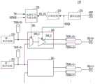
参考图1,根据本公开的实施例的存储系统100可以特别包括形成在中介层130和封装基板140上方的存储器件110和处理器120。Referring to FIG. 1 , a
如图1所示,中介层130形成在封装基板140上方,并且存储器件110和处理器120形成在中介层130上方。中介层130可以是在一个连接与另一连接之间进行路由的电接口。通过使用中介层130,可以将一连接重新路由到不同的连接,和/或可以将一连接扩展到更宽的间距。中介层130的作用是在处理器120和存储器件110之间提供路径,因此,中介层130所提供的电互连路径在存储器件110和处理器120之间提供了更紧密的集成。因此,中介层130可以为处理器120与存储器件110之间的高速通信提供有效的方式。中介层130(其可以是硅芯片,但是是无源的而没有晶体管)可以提供密度更大的配置,该配置在给定的区域中比片外封装(off-chip package)具有更多的连接和走线。As shown in FIG. 1 , the
在图1中,处理器120可以执行存储器控制功能。处理器120可以是存储器控制器,或者存储器控制器可以被集成到处理器120中作为其的一部分。因此,处理器120特别包括管理数据流入和流出存储器件110的数字电路。处理器120可以包括各种处理器,例如中央处理单元(CPU)、图形处理单元(GPU)以及应用处理器(AP)。存储器控制器120和存储器件110中的每一个具有接口PHY,并且存储器控制器120和存储器件110的相应接口PHY通过中介层130彼此耦接。In FIG. 1, a
存储器件110包括多个集成电路芯片112和114。图1中所示的存储器件110是具有彼此层叠在顶部上的多个裸片112和114的三维(3D)半导体器件。这种三维(3D)层叠减少了占位面积,并使得封装的整体尺寸更小,并且可以适用于高带宽存储操作而同时所需功耗更低。三维集成存储器件110包括具有用于与处理器120通信的逻辑电路的基底裸片114(或也称为第一集成电路芯片114)和层叠在基底裸片114上的多个核心裸片112(或也称为第二集成电路芯片112)。The
如图1所示,基底裸片114通过穿通硅通孔(TSV)或穿通电极和微凸块与核心裸片112互连。存储器件110的垂直层叠的裸片112和114通过穿通硅通孔(TSV)或穿通电极互连,并通过中介层130与处理器120通信。由于存储器件110被设置得如此靠近处理器120,并且经由中介层130互连,因此它们之间存在较短的数据路径。较短的数据路径与存储器件110的宽的存储器总线相结合,意味着处理器120可以以较低的潜伏时间与存储器件110进行高速通信。As shown in FIG. 1 , the
例如,存储器件110可以是高带宽存储器(HBM),尽管本公开的存储器件110的范围不仅限于高带宽存储器(HBM)。作为高带宽存储器(HBM),存储器件110可以例如包括用于3D层叠DRAM裸片112的高性能RAM接口114,其可以与处理器120结合使用,如上所述,处理器120可以是诸如GPU、CPU、AP等的高性能处理器。For example, the
基底裸片(即,第一集成电路芯片)114,其通过穿通硅通孔(TSV)或穿通电极与垂直层叠的核心裸片112电耦接,可以通过接口PHY向/从处理器120发送/接收数据。The base die (ie, the first integrated circuit chip) 114, which is electrically coupled to the vertically stacked core die 112 through through-silicon vias (TSVs) or through electrodes, can send/from the
每个核心裸片112可以包括用于在其中储存数据的单元阵列以及用于向单元阵列写入数据和从单元阵列读取数据的电路。另一方面,基底裸片114可以包括用于与核心裸片112和处理器120进行接口的逻辑电路。以这种方式配置,显著地增加了存储器件110的输入/输出单元的数量,从而有效地增加了带宽。如上所述,以这种方式配置的存储器件110的示例可以包括高带宽存储器(HBM)。Each core die 112 may include a cell array for storing data therein and circuitry for writing data to and reading data from the cell array. On the other hand, base die 114 may include logic circuitry for interfacing with core die 112 and
基底裸片114和核心裸片112可以分别被制造,然后彼此耦接。在将基底裸片114和核心裸片112耦接之前,可以分别测试它们。也就是说,为了测试基底裸片114是否具有缺陷,在将基底裸片114耦接到核心裸片112之前,基底裸片114可以输入/输出数据。可以将测试配置为在每个级别测试不良裸片。即,可以在将裸片112和裸片114安装成层叠之前分别对它们进行测试,或者也可以在它们被层叠之后对它们进行测试。然而,在安装裸片112和裸片114之前分别对它们进行测试将提供的优势在于,能够在封装之前仅丢弃有缺陷的裸片而不是整个裸片层叠。Base die 114 and core die 112 may be fabricated separately and then coupled to each other. Before coupling the base die 114 and the core die 112, they may be tested separately. That is, to test whether the base die 114 has defects, the base die 114 may input/output data prior to coupling the base die 114 to the core die 112 . Tests can be configured to test bad dies at each level. That is, the
在每个裸片112或114中可以形成有成千上万的穿通硅通孔(TSV)和相应的焊盘。垂直层叠的核心裸片112的最顶部裸片可以不需要穿通硅通孔(TSV)或穿通电极;然而,出于制造方便或出于其他原因,核心裸片112的最顶部裸片仍可以可选地设置有穿通硅通孔(TSV)或穿通电极。穿通硅通孔(TSV)或穿通电极执行作为用于数据传输、I/O、电源等的有效路径的功能,但是穿通硅通孔(TSV)或穿通电极在设计时要考虑冗余。这样,穿通硅通孔(TSV)或穿通电极本身也被测试,以准确确定哪些TSV有缺陷并且无法满足性能预期。然后可以用冗余的穿通硅通孔(TSV)或穿通电极来替换有缺陷的穿通硅通孔(TSV)或穿通电极。即使在将裸片安装成垂直层叠之后才发现有缺陷的穿通硅通孔(TSV),也仅用冗余的穿通硅通孔(TSV)或穿通电极来替换通过测试而确定的有缺陷的穿通硅通孔(TSV)或穿通电极。即使在安装之后才发现有缺陷的穿通硅通孔(TSV),也可以通过保留垂直层叠的裸片的功能完整性(而不是必须丢弃整个裸片层叠)来消除浪费并提高成品率。Thousands of through silicon vias (TSVs) and corresponding pads may be formed in each die 112 or 114 . The topmost die of the vertically stacked core dies 112 may not require through silicon vias (TSVs) or through electrodes; however, the topmost die of the core dies 112 may still be available for manufacturing convenience or for other reasons. Through silicon vias (TSVs) or through electrodes are optionally provided. Through silicon vias (TSVs) or through electrodes perform functions as efficient paths for data transfer, I/O, power, etc., but through silicon vias (TSVs) or through electrodes are designed with redundancy in mind. In this way, through silicon vias (TSVs) or through electrodes themselves are also tested to determine exactly which TSVs are defective and fail to meet performance expectations. Defective through silicon vias (TSVs) or through electrodes can then be replaced with redundant through silicon vias (TSVs) or through electrodes. Even if the defective through silicon vias (TSVs) are discovered after the die is mounted in a vertical stack, only redundant through silicon vias (TSVs) or through electrodes are used to replace the defective through silicon vias (TSVs) determined by testing Through Silicon Vias (TSVs) or through electrodes. Even if defective through-silicon vias (TSVs) are discovered after installation, waste can be eliminated and yield improved by preserving the functional integrity of the vertically stacked die (rather than having to discard the entire die stack).
与核心裸片112不同,基底裸片114可以不具有用于储存数据的单元阵列,并且在没有单元阵列的情况下,测试基底裸片114可能是困难的过程,因为将难以生成例如用于测试基底裸片114的输入/输出线所需的各种模式的数据。当在层叠所述芯片之前对基底裸片114执行晶圆测试时,由于因在基底裸片114中缺乏单元阵列而无法生成各种模式的测试信号,因此对用于执行读取和写入操作的信号线的测试、对检查每个数据总线的建立/保持余量的测试、对缺陷筛选和其他输入/输出性能等的测试将会是困难的。Unlike core die 112, base die 114 may not have a cell array for storing data, and without a cell array, testing base die 114 may be a difficult process because it would be difficult to generate, for example, for testing Various patterns of data required by the input/output lines of the base die 114 . When wafer testing is performed on the base die 114 prior to stacking the chips, since various patterns of test signals cannot be generated due to the lack of a cell array in the base die 114, read and write operations are performed on the base die 114. It will be difficult to test the signal lines of the original data bus, test to check the setup/hold margin of each data bus, test for defect screening and other input/output performance, etc.
然而,根据本公开的实施例,提供了在层叠之前单独地测试不具有单元阵列的基底裸片114的各种方式。基底裸片114设置有用于修复有缺陷的穿通硅通孔(TSV)或穿通电极的修复电路,但是直到将基底裸片114安装为垂直层叠中的基底裸片时,可能都不需要该穿通硅通孔(TSV)修复电路。更具体地,穿通硅通孔(TSV)修复电路可以包括选择电路(例如,包括多路复用器MUX的电路),该选择电路用于选择例如冗余的穿通硅通孔(TSV)或穿通电极,以便用无缺陷的穿通硅通孔(TSV)或穿通电极来替换有缺陷的穿通硅通孔(TSV)或穿通电极。然而,当单独地测试基底裸片114时,该穿通硅通孔(TSV)修复电路不一定会被需要或使用。根据本公开的实施例,在仅有基底裸片114的测试期间,具有选择电路的穿通硅通孔(TSV)修复电路被用于生成各种模式的测试数据,因此,即使在基底裸片114中未配备任何单元阵列,仅有基底裸片114的晶圆级测试也是可能的。However, in accordance with embodiments of the present disclosure, various ways of individually testing the base dies 114 without the cell array prior to stacking are provided. Base die 114 is provided with repair circuitry for repairing defective through silicon vias (TSVs) or through electrodes, but may not be needed until base die 114 is mounted as a base die in a vertical stack Through hole (TSV) repair circuit. More specifically, a through silicon via (TSV) repair circuit may include a selection circuit (eg, a circuit including a multiplexer MUX) for selecting, for example, redundant through silicon vias (TSVs) or through Electrodes to replace defective through silicon vias (TSVs) or through electrodes with non-defective through silicon vias (TSVs) or through electrodes. However, this through silicon via (TSV) repair circuit may not necessarily be required or used when the base die 114 is tested individually. According to embodiments of the present disclosure, during testing of only the base die 114 , through-silicon via (TSV) repair circuits with select circuits are used to generate various patterns of test data, therefore, even when the base die 114 is tested No cell arrays are provided in the device, wafer level testing of only the base die 114 is also possible.
现在参考图2,将根据本公开的实施例更详细地描述基底裸片(或第一集成电路芯片)114的与数据传输有关的一部分。Referring now to FIG. 2, a portion of the base die (or first integrated circuit chip) 114 related to data transfer will be described in more detail in accordance with embodiments of the present disclosure.
第一集成电路芯片114特别包括解码电路210、分频电路220、选择信号生成电路230、传输电路240和241、锁存电路250和251、穿通硅通孔(TSV)或穿通电极TSVR<0>和TSVR<1>、以及数据节点DQ<0>和DQ<1>。The first
如上所述,第一集成电路芯片114可以包括垂直穿通其内部而形成的多个穿通电极,如TSVR<0>和TSVR<1>。当在多个穿通电极TSVR<0>和TSVR<1>中的一个中出现缺陷时,第一集成电路芯片114可以用相邻的穿通电极或另一个穿通电极来替换有缺陷的穿通电极。As described above, the first
图2示出了第一集成电路芯片114的多个穿通电极中的第一穿通电极TSVR<0>和第二穿通电极TSVR<1>。类似地,在图2中,第一集成电路芯片114包括第一传输电路240和第二传输电路241、第一锁存电路250和第二锁存电路251、以及分别与第一穿通电极TSVR<0>和第二穿通电极TSVR<1>对应的第一数据节点DQ<0>和第二数据节点DQ<1>。然而,应注意的是,本实施例的范围不限于此。FIG. 2 shows a first through electrode TSVR<0> and a second through electrode TSVR<1> among the plurality of through electrodes of the first
分别对应于第一穿通电极TSVR<0>和第二穿通电极TSVR<1>的第一数据节点DQ<0>和第二数据节点DQ<1>用作用于向/从存储器控制器120发送/接收数据的节点。第一数据节点DQ<0>和第二数据节点DQ<1>可以通过微凸块等连接到中介层130,并且可以通过中介层130连接到存储器控制器120的接口PHY。The first data node DQ<0> and the second data node DQ<1> respectively corresponding to the first through electrode TSVR<0> and the second through electrode TSVR<1> are used for transmitting/to/from the
第一锁存电路250和第二锁存电路251可以储存通过第一穿通电极TSVR<0>和第二穿通电极TSVR<1>发送/接收的数据。在写入操作期间,通过第一数据节点DQ<0>和第二数据节点DQ<1>输入的数据可以储存在第一锁存电路250和第二锁存电路251中,并传输到相应的第一穿通电极TSVR<0>和第二穿通电极TSVR<1>。在读取操作期间,从第二集成电路芯片112读取的数据可以分别储存在第一锁存电路250和第二锁存电路251中以通过第一穿通电极TSVR<0>和第二穿通电极TSVR<1>进行传输。在根据本公开的实施例的测试操作期间,可以通过第一数据节点DQ<0>和第二数据节点DQ<1>输入具有不同逻辑电平的数据,并且可以分别将其储存在第一锁存电路250和第二锁存电路251中。The
来自第一穿通电极TSVR<0>和第二穿通电极TSVR<1>的信号通过第一传输电路240和第二传输电路241被传输到第一数据节点DQ<0>和第二数据节点DQ<1>。即,在读取操作期间,从第二集成电路芯片112读取的数据通过第一穿通电极TSVR<0>和第二穿通电极TSVR<1>输入,并且第一传输电路240和第二传输电路241可以用于将输入数据通过数据线TIORL<0:1>和TIORH<0:1>传输到第一数据节点DQ<0>和第二数据节点DQ<1>。第一传输电路240和第二传输电路241可以对输入数据进行串行至并行转换,并将转换的数据传输至数据线TIORL<0:1>和TIORH<0:1>。如图2所示是用于以1:2的比率进行数据的串行至并行转换的操作,但是本实施例的范围不限于此。Signals from the first through electrode TSVR<0> and the second through electrode TSVR<1> are transmitted to the first and second data nodes DQ<0> and DQ< through the
第一传输电路240可以响应于选择信号SEL来选择通过第一穿通电极TSVR<0>传输的信号和通过第二穿通电极TSVR<1>传输的信号中的一者,并且将选择的信号传输至第一数据节点DQ<0>。根据实施例,在测试操作期间,第一传输电路240可以响应于选择信号SEL而交替地将储存在第一锁存电路250和第二锁存电路251中的数据传输到第一数据节点DQ<0>。即,由于在测试操作期间具有不同逻辑电平的数据被储存在第一锁存电路250和第二锁存电路251中,因此第一传输电路240可以将触发(toggle)至不同逻辑电平的数据传输至第一数据节点DQ<0>。The
第一传输电路240可以包括选择器240_1和读取驱动器240_2。选择器240_1可以响应于选择信号SEL来选择通过第一穿通电极TSVR<0>传输的信号和通过第二穿通电极TSVR<1>传输的信号中的一者。读取驱动器240_2可以响应于读取数据选通信号RDQS将由选择器240_1选择的信号传输到第一数据节点DQ<0>。The
例如,当选择信号SEL被去激活为逻辑低电平时,选择器240_1可以选择通过第一穿通电极TSVR<0>传输的信号。另一方面,当选择信号SEL被激活到逻辑高电平时,选择器240_1可以选择通过第二穿通电极TSVR<1>传输的信号。因此,当选择信号SEL被去激活为逻辑低电平时,读取驱动器240_2可以将通过第一穿通电极TSVR<0>传输的信号传输到第一数据节点DQ<0>,并且当选择信号SEL被激活为逻辑高电平时,读取驱动器240_2可以将通过第二穿通电极TSVR<1>传输的信号传输到第一数据节点DQ<0>。For example, when the selection signal SEL is deactivated to a logic low level, the selector 240_1 may select a signal transmitted through the first through electrode TSVR<0>. On the other hand, when the selection signal SEL is activated to a logic high level, the selector 240_1 may select a signal transmitted through the second through electrode TSVR<1>. Therefore, when the selection signal SEL is deactivated to a logic low level, the read driver 240_2 may transfer the signal transmitted through the first through electrode TSVR<0> to the first data node DQ<0>, and when the selection signal SEL is deactivated When activated as a logic high level, the read driver 240_2 may transmit the signal transmitted through the second through electrode TSVR<1> to the first data node DQ<0>.
与第一传输电路240的操作相似,第二传输电路241可以响应于第二穿通电极TSVR<1>和第三穿通电极(图2中未示出)而操作。因此,在此将省略对第二传输电路241的操作的重复描述。Similar to the operation of the
解码电路210可以通过对从存储器控制器120输入的命令/地址进行解码来生成用于控制内部操作的信号。在读取操作期间,解码电路210可以通过对列地址ADD进行解码来生成读取命令信号。解码电路210可以通过将该读取命令信号与时钟同步来生成用于控制读取操作的信号,即,读取数据选通信号RDQS。The
分频电路220可以通过对经由解码电路210生成的读取数据选通信号RDQS进行分频来生成分频信号RD_OD。分频电路220可以通过将读取数据选通信号RDQS的周期加倍来生成分频信号RD_OD。The
根据实施例,在正常操作期间,选择信号生成电路230可以基于修复信息来生成选择信号SEL。另一方面,在测试操作期间,选择信号生成电路230可以使用分频信号RD_OD来生成选择信号SEL,或触发的选择信号SEL。选择信号生成电路230可以接收测试模式信号TM、修复信息信号REPAIR和分频信号RD_OD,根据本公开的实施例将参考图4更详细地描述选择信号生成电路230的配置和操作。According to an embodiment, during normal operation, the selection
参考图3,图2的分频电路220特别包括:串联耦接的第一传送单元310和第二传送单元320。Referring to FIG. 3 , the
第一传送单元310可以响应于读取数据选通信号RDQS将反馈的分频信号RD_OD传送到第二传送单元320。当读取数据选通信号RDQS在逻辑高电平被去激活时,三态反相器311和锁存器314可以被关断,并且三态反相器312和313可以被导通。当读取数据选通信号RDQS被激活为逻辑低电平时,三态反相器311和锁存器314可以被导通。当通过这样的操作将读取数据选通信号RDQS激活为逻辑低电平时,反馈的分频信号RD_OD可以被传送到第二传送单元320。第一传送单元310可以进一步包括接收复位信号RSTB的与非门315和反相器316。当复位信号RSTB被激活为逻辑低电平时,第一传送单元310可以被复位。The
第二传送单元320可以响应于读取数据选通信号RDQS将第一传送单元310的输出信号反相,并输出该反相的信号作为分频信号RD_OD。当读取数据选通信号RDQS在逻辑高电平被去激活时,三态反相器321和锁存器324可以被关断,并且三态反相器322和323可以被导通。当读取数据选通信号RDQS被激活为逻辑低电平时,三态反相器321和锁存器324可以被导通。当通过这样的操作将读取数据选通信号RDQS激活为逻辑低电平时,第二传送单元320可以将第一传送单元310的输出信号反相,并且输出反相的信号作为分频信号RD_OD。第二传送单元320可以进一步包括接收复位信号RSTB的反相器326和或非门325。当复位信号RSTB被激活为逻辑低电平时,第二传送单元320可以被复位。The
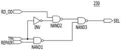
图4示出了根据本公开实施例的图2的选择信号生成电路230。选择信号生成电路230可以特别包括反相器INV以及第一门NAND1、第二门NAND2和第三门NAND3,根据本公开的实施例,第一、第二和第三门全都是与非门。但是,也可以通过其他逻辑门的组合来执行相同的逻辑运算。FIG. 4 illustrates the selection
第一门NAND1可以接收测试模式信号TM和修复信息信号REPAIR。第一门NAND1可以对测试模式信号TM和修复信息信号REPAIR执行与非逻辑运算,并且输出与非逻辑运算的结果值。The first gate NAND1 may receive the test mode signal TM and the repair information signal REPAIR. The first gate NAND1 may perform a NAND logic operation on the test mode signal TM and the repair information signal REPAIR, and output a result value of the NAND logic operation.
第二门NAND2可以接收分频信号RD_OD和由反相器INV反相的测试模式信号TM。第二门NAND2可以对分频信号RD_OD和反相的测试模式信号TM执行与非逻辑运算,并且输出与非逻辑运算的结果值。The second gate NAND2 may receive the frequency-divided signal RD_OD and the test mode signal TM inverted by the inverter INV. The second gate NAND2 may perform a NAND logic operation on the frequency-divided signal RD_OD and the inverted test mode signal TM, and output a result value of the NAND logic operation.
第三门NAND3可以接收第一门NAND1和第二门NAND2的输出信号。第三门NAND3可以对第一门NAND1和第二门NAND2的输出信号执行与非逻辑运算,并且输出与非逻辑运算的结果值作为选择信号SEL。The third gate NAND3 may receive output signals of the first gate NAND1 and the second gate NAND2. The third gate NAND3 may perform a NAND logic operation on the output signals of the first gate NAND1 and the second gate NAND2, and output a result value of the NAND logic operation as a selection signal SEL.
根据实施例,当第一集成电路芯片114执行正常操作时,可以将测试模式信号TM去激活为逻辑高电平。当测试模式信号TM处于逻辑高电平时,第一门NAND1可以根据修复信息信号REPAIR来激活或去激活输出信号。另一方面,第二门NAND2可以输出高电平的输出信号,无论分频信号RD_OD如何。因此,第三门NAND3可以根据第一门NAND1的输出信号来激活或去激活选择信号SEL。According to an embodiment, when the first
当第一集成电路芯片114执行正常操作时,选择信号生成电路230可以根据修复信息信号REPAIR来激活或去激活选择信号SEL。修复信息信号REPAIR可以根据在第一穿通电极TSVR<0>中是否检测到缺陷而被激活或去激活。When the first
例如,当在第一穿通电极TSVR<0>中未检测到缺陷时,可以将修复信息信号REPAIR去激活为逻辑低电平。根据低电平的修复信息信号REPAIR,选择信号生成电路230可以将选择信号SEL去激活为逻辑低电平。如上所述,当选择信号SEL处于逻辑低电平时,第一传输电路240可以选择通过第一穿通电极TSVR<0>传输的信号,并且将选择的信号传输至第一数据节点DQ<0>。For example, when no defect is detected in the first through electrode TSVR<0>, the repair information signal REPAIR may be deactivated to a logic low level. According to the repair information signal REPAIR at a low level, the selection
另一方面,当在第一穿通电极TSVR<0>中检测到缺陷时,修复信息信号REPAIR可以被激活为逻辑高电平。根据高电平的修复信息信号REPAIR,选择信号生成电路230可以将选择信号SEL激活为逻辑高电平。如上所述,当选择信号SEL处于逻辑高电平时,第一传输电路240可以选择通过第二穿通电极TSVR<1>传输的信号,并将选择的信号传输至第一数据节点DQ<0>。On the other hand, when a defect is detected in the first through electrode TSVR<0>, the repair information signal REPAIR may be activated to a logic high level. According to the repair information signal REPAIR at a high level, the selection
根据实施例,当第一集成电路芯片114执行测试操作时,测试模式信号TM可以被激活为逻辑低电平。当对第一集成电路芯片114执行晶圆级测试时,测试模式信号TM可以被激活为逻辑低电平。然而,本实施例的范围不限于此。According to an embodiment, when the first
当测试模式信号TM处于逻辑低电平时,第一门NAND1可以输出高电平的输出信号,无论修复信息信号REPAIR如何。另一方面,第二门NAND2可以根据分频信号RD_OD来激活或去激活输出信号。因此,第三门NAND3可以根据第二门NAND2的输出信号来激活或去激活选择信号SEL。When the test mode signal TM is at a logic low level, the first gate NAND1 may output a high level output signal regardless of the repair information signal REPAIR. On the other hand, the second gate NAND2 may activate or deactivate the output signal according to the frequency division signal RD_OD. Therefore, the third gate NAND3 may activate or deactivate the selection signal SEL according to the output signal of the second gate NAND2.
当第一集成电路芯片114执行测试操作时,选择信号生成电路230可以根据分频信号RD_OD来激活或去激活选择信号SEL。由于分频信号RD_OD根据读取数据选通信号RDQS触发,因此在读取操作期间选择信号生成电路230可以通过触发选择信号SEL来生成选择信号SEL。第一传输电路240可以交替地将储存在第一锁存电路250和第二锁存电路251中的数据传输到第一数据节点DQ<0>。When the first
图5示出了根据本公开的实施例的图2的第一集成电路芯片114的信号波形。FIG. 5 illustrates signal waveforms of the first
图5示出了由第一传输电路240从第一穿通电极TSVR<0>和第二穿通电极TSVR<1>传输到第一数据节点DQ<0>的数据的波形以及用于控制该数据的信号的波形。如上所述,传输到第一数据节点DQ<0>的数据可以通过第一数据线TIORL<0>和第二数据线TIORH<0>并行传输。因此,如图5所示是与数据有关的多个控制信号。FIG. 5 shows waveforms of data transferred from the first through electrode TSVR<0> and the second through electrode TSVR<1> to the first data node DQ<0> by the
当在第一集成电路芯片114进入测试模式之后开始写入操作时,可以通过第一数据节点DQ<0>和第二数据节点DQ<1>输入测试数据。测试数据可以被传输到第一穿通电极TSVR<0>和第二穿通电极TSVR<1>,并且最终被储存在第一锁存电路250和第二锁存电路251中。When the write operation is started after the first
根据实施例,可以将具有彼此不同的逻辑电平(例如,1:0)的第一数据和第二数据分别储存在与第一穿通电极TSVR<0>和第二穿通电极TSVR<1>相对应的第一锁存电路250和第二锁存电路251中。测试数据可以是触发数据(toggling data)。尽管通过第一数据节点DQ<0>和第二数据节点DQ<1>输入的测试数据是触发的,但最后的输入数据可以具有不同的值。According to an embodiment, the first data and the second data having different logic levels (eg, 1:0) from each other may be stored in phases with the first through electrode TSVR<0> and the second through electrode TSVR<1>, respectively. in the corresponding
当在写入操作之后开始读取操作时,解码电路210可以通过对列地址ADD进行解码来生成第一读取数据选通信号RDQSL和第二读取数据选通信号RDQSH。分频电路220可以通过对第一读取数据选通信号RDQSL和第二读取数据选通信号RDQSH进行分频来生成第一分频信号RD_ODL和第二分频信号RD_ODH。When the read operation is started after the write operation, the
每当第一读取数据选通信号RDQSL和第二读取数据选通信号RDQSH转变为逻辑低电平时,第一分频信号RD_ODL和第二分频信号RD_ODH的逻辑电平可以转变。第一分频信号RD_ODL和第二分频信号RD_ODH可以具有通过使第一读取数据选通信号RDQSL和第二读取数据选通信号RDQSH的周期加倍而增加的周期。每当第一读取数据选通信号RDQSL和第二读取数据选通信号RDQSH被激活时,第一分频信号RD_ODL和第二分频信号RD_ODH可以交替地具有高电平值和低电平值。可以根据实施例以各种方式执行分频方法或操作,并且本实施例不限于此。Whenever the first read data strobe signal RDQSL and the second read data strobe signal RDQSH transition to a logic low level, the logic levels of the first frequency division signal RD_ODL and the second frequency division signal RD_ODH may transition. The first and second frequency-divided signals RD_ODL and RD_ODH may have periods increased by doubling periods of the first and second read data strobe signals RDQSL and RDQSH. Whenever the first read data strobe signal RDQSL and the second read data strobe signal RDQSH are activated, the first frequency division signal RD_ODL and the second frequency division signal RD_ODH may alternately have a high level value and a low level value. The frequency dividing method or operation may be performed in various ways according to the embodiment, and the embodiment is not limited thereto.
因此,当第一数据选通信号RDQSL被第一次激活(在图5中,用带圆圈的“1”①来标记)时,第一分频信号RD_ODL可以具有逻辑低电平。选择信号生成电路230可以响应于低电平的分频信号RD_ODL将选择信号SEL去激活为逻辑低电平。当选择信号SEL处于逻辑低电平时,选择器240_1可以选择储存在第一穿通电极TSVR<0>(即,第一锁存电路250)中的第一数据1。读取驱动器240_2可以响应于第一读取数据选通信号RDQSL将选择的第一数据1传输至第一数据线TIORL<0>。Therefore, when the first data strobe signal RDQSL is activated for the first time (marked with a circled "1" ① in FIG. 5 ), the first frequency division signal RD_ODL may have a logic low level. The selection
然后,当第一数据选通信号RDQSL被第二次激活(在图5中,用带圆圈的“2”②来标记)时,第一分频信号RD_ODL可以具有逻辑高电平。选择信号生成电路230可以响应于高电平的分频信号RD_ODL将选择信号SEL激活为逻辑高电平。当选择信号SEL处于逻辑高电平时,选择器240_1可以选择储存在第二穿通电极TSVR<1>(即,第二锁存电路251)中的第二数据0。读取驱动器240_2可以响应于第一读取数据选通信号RDQSL将选择的第二数据0传输至第一数据线TIORL<0>。Then, when the first data strobe signal RDQSL is activated for the second time (marked with a circled "2" ② in FIG. 5 ), the first frequency division signal RD_ODL may have a logic high level. The selection
类似地,当第二读取数据选通信号RDQSH被第一次激活(在图5中,用带圆圈的“3”③来标记)并且第二分频信号RD_ODH具有逻辑低电平时,选择信号生成电路230可以将选择信号SEL去激活为逻辑低电平。第一传输电路240可以选择储存在第一穿通电极TSVR<0>(即,第一锁存电路250)中的第一数据1,并且将选择的数据传输到第二数据线TIORH<0>。当第二读取数据选通信号RDQSH被第二次激活(在图5中,用带圆圈的“4”④来标记)并且第二分频信号RD_ODH具有逻辑高电平时,选择信号生成电路230可以将选择信号SEL激活为逻辑高电平。第一传输电路240可以选择储存在第二穿通电极TSVR<1>(即,第二锁存电路251)中的第二数据0,并且将选择的数据传输到第二数据线TIORH<0>。Similarly, when the second read data strobe signal RDQSH is activated for the first time (marked with a circled "3" ③ in FIG. 5 ) and the second frequency division signal RD_ODH has a logic low level, the selection signal The
根据本公开的实施例,集成电路芯片可以使用用于控制读取操作的读取数据选通信号RDQSL和RDQSH来触发要通过数据线TIORL<0>和TIORH<0>传输的数据。即,集成电路芯片可以根据数据的带宽来传输逻辑高电平和逻辑低电平的数据,从而检查数据线TIORL<0>和TIORH<0>的建立/保持余量或者检测缺陷。According to an embodiment of the present disclosure, the integrated circuit chip may use read data strobe signals RDQSL and RDQSH for controlling a read operation to trigger data to be transmitted through the data lines TIORL<0> and TIORH<0>. That is, the integrated circuit chip can transmit data of logic high level and logic low level according to the bandwidth of the data, thereby checking the setup/hold margins of the data lines TIORL<0> and TIORH<0> or detecting defects.
根据本公开的实施例,集成电路芯片可以通过切换数据路径来触发通过数据路径而传输的数据。特别地,即使像基底裸片一样的情况在集成电路芯片中未设置存储单元阵列,集成电路芯片也可以将触发数据传输到数据路径,并检查数据路径的建立/保持余量或者检测缺陷。此外,由于集成电路芯片可以使用安装在基底裸片中的修复电路来切换数据路径,因此可以测试数据输入/输出线而无需另外的电路配置或增加信号负载。According to an embodiment of the present disclosure, the integrated circuit chip can trigger data transmitted through the data path by switching the data path. In particular, even if the memory cell array is not provided in the integrated circuit chip as in the case of the base die, the integrated circuit chip can transmit trigger data to the data path and check the setup/hold margin of the data path or detect defects. Furthermore, since the integrated circuit chip can switch data paths using repair circuits mounted in the base die, data input/output lines can be tested without additional circuit configuration or increased signal loading.
尽管出于说明性目的描述了各种实施例,但是对本领域技术人员显而易见的是,在不脱离如所附权利要求书所限定的本发明的精神和范围的情况下,可以进行各种改变和修改。While various embodiments have been described for illustrative purposes, it will be apparent to those skilled in the art that various changes and modifications can be made therein without departing from the spirit and scope of the invention as defined by the appended claims. Revise.
Claims (24)
Translated fromChineseApplications Claiming Priority (2)
| Application Number | Priority Date | Filing Date | Title |
|---|---|---|---|
| KR1020190000682AKR102739815B1 (en) | 2019-01-03 | 2019-01-03 | Integrated circuit chip |
| KR10-2019-0000682 | 2019-01-03 |
Publications (2)
| Publication Number | Publication Date |
|---|---|
| CN111402945Atrue CN111402945A (en) | 2020-07-10 |
| CN111402945B CN111402945B (en) | 2023-09-29 |
Family
ID=71405151
Family Applications (1)
| Application Number | Title | Priority Date | Filing Date |
|---|---|---|---|
| CN201911251874.3AActiveCN111402945B (en) | 2019-01-03 | 2019-12-09 | Integrated circuit chip and die testing without cell array |
Country Status (3)
| Country | Link |
|---|---|
| US (2) | US12009043B2 (en) |
| KR (1) | KR102739815B1 (en) |
| CN (1) | CN111402945B (en) |
Cited By (4)
| Publication number | Priority date | Publication date | Assignee | Title |
|---|---|---|---|---|
| CN107688694A (en)* | 2016-08-05 | 2018-02-13 | 新思科技有限公司 | Defect sign and waveform analysis are perceived using the unit of multiple gating points |
| CN115547404A (en)* | 2022-11-30 | 2022-12-30 | 普赛微科技(杭州)有限公司 | Test architecture and method for advanced packaging of MRAM memory |
| WO2024244923A1 (en)* | 2023-05-26 | 2024-12-05 | 长鑫科技集团股份有限公司 | Semiconductor chip, semiconductor structure and semiconductor device |
| WO2025129731A1 (en)* | 2023-12-18 | 2025-06-26 | 长鑫科技集团股份有限公司 | Memory chip, logic chip, chip stacking structure, and memory |
Families Citing this family (4)
| Publication number | Priority date | Publication date | Assignee | Title |
|---|---|---|---|---|
| KR102791111B1 (en)* | 2020-02-03 | 2025-04-07 | 삼성전자주식회사 | Stacked memory device, and operating method thereof |
| KR102732814B1 (en) | 2020-07-09 | 2024-11-20 | 현대모비스 주식회사 | Braking Apparatus for Vehicle |
| US12241931B1 (en)* | 2022-01-12 | 2025-03-04 | Marvell Asia Pte Ltd | Method and apparatus for capture clock control to minimize toggling during testing |
| US20230395566A1 (en)* | 2022-06-02 | 2023-12-07 | Micron Technology, Inc. | Repeater scheme for inter-die signals in multi-die package |
Citations (18)
| Publication number | Priority date | Publication date | Assignee | Title |
|---|---|---|---|---|
| CN101494088A (en)* | 2008-01-25 | 2009-07-29 | 恩益禧电子股份有限公司 | Semiconductor integrated circuit device and method of testing same |
| US20100060310A1 (en)* | 2008-09-10 | 2010-03-11 | Qualcomm Incorporated | Systems and Methods Utilizing Redundancy in Semiconductor Chip Interconnects |
| US20100295600A1 (en)* | 2009-05-20 | 2010-11-25 | Qualcomm Incorporated | Method and Apparatus for Providing Through Silicon VIA (TSV) Redundancy |
| US20110006391A1 (en)* | 2009-07-10 | 2011-01-13 | Jeong-Woo Lee | Semiconductor device |
| US20120104388A1 (en)* | 2010-10-29 | 2012-05-03 | Hynix Semiconductor Inc. | Three-dimensional stacked semiconductor integrated circuit and tsv repair method thereof |
| CN102520340A (en)* | 2012-01-06 | 2012-06-27 | 日月光半导体制造股份有限公司 | Semiconductor package component with test structure and test method thereof |
| CN102539852A (en)* | 2012-03-14 | 2012-07-04 | 中南大学 | Test head for automatically detecting wafer-level packaged chips and implementing method for test head |
| CN102592647A (en)* | 2011-01-14 | 2012-07-18 | 海力士半导体有限公司 | Semiconductor apparatus, method for assigning chip IDs therein, and method for setting chip IDs |
| CN102655101A (en)* | 2012-03-30 | 2012-09-05 | 北京大学 | Built-in self test and built-in self-repairing technology of TSV (Through Silicon Via) interconnection of 3D chip |
| CN102738119A (en)* | 2011-04-13 | 2012-10-17 | 台湾积体电路制造股份有限公司 | Through-silicon vias for semicondcutor substrate and method of manufacture |
| US8339879B2 (en)* | 2009-11-30 | 2012-12-25 | SK Hynix Inc. | Repair circuit and semiconductor apparatus including the same |
| KR20140030608A (en)* | 2012-09-03 | 2014-03-12 | 에스케이하이닉스 주식회사 | Tsv structure of semiconductor memory device and testing method thereof |
| US8717839B2 (en)* | 2011-02-22 | 2014-05-06 | Elpida Memory, Inc. | Semiconductor device having plural penetration electrodes penetrating through semiconductor substrate and testing method thereof |
| US8917569B2 (en)* | 2011-01-31 | 2014-12-23 | SK Hynix Inc. | Semiconductor apparatus transmitting fuse information and repair method thereof |
| US20160141014A1 (en)* | 2012-06-29 | 2016-05-19 | SK Hynix Inc. | Semiconductor integrated circuit |
| US20180107387A1 (en)* | 2016-07-13 | 2018-04-19 | Samsung Electronics Co., Ltd. | Interface circuits configured to interface with multi-rank memory |
| CN109037193A (en)* | 2018-09-05 | 2018-12-18 | 长鑫存储技术有限公司 | Through silicon via detection circuit and method, IC chip |
| CN109037192A (en)* | 2018-08-31 | 2018-12-18 | 长鑫存储技术有限公司 | Through silicon via fault tolerable circuit and method, integrated circuit |
Family Cites Families (3)
| Publication number | Priority date | Publication date | Assignee | Title |
|---|---|---|---|---|
| KR102146470B1 (en) | 2014-01-17 | 2020-08-21 | 에스케이하이닉스 주식회사 | Semiconductor appratus having through silicon via |
| US10083722B2 (en)* | 2016-06-08 | 2018-09-25 | Samsung Electronics Co., Ltd. | Memory device for performing internal process and operating method thereof |
| US10468386B1 (en)* | 2018-11-08 | 2019-11-05 | Micron Technology, Inc. | TSV redundancy and TSV test select scheme |
- 2019
- 2019-01-03KRKR1020190000682Apatent/KR102739815B1/enactiveActive
- 2019-10-29USUS16/667,738patent/US12009043B2/enactiveActive
- 2019-12-09CNCN201911251874.3Apatent/CN111402945B/enactiveActive
- 2024
- 2024-04-01USUS18/623,201patent/US20240257897A1/enactivePending
Patent Citations (20)
| Publication number | Priority date | Publication date | Assignee | Title |
|---|---|---|---|---|
| CN101494088A (en)* | 2008-01-25 | 2009-07-29 | 恩益禧电子股份有限公司 | Semiconductor integrated circuit device and method of testing same |
| US20100060310A1 (en)* | 2008-09-10 | 2010-03-11 | Qualcomm Incorporated | Systems and Methods Utilizing Redundancy in Semiconductor Chip Interconnects |
| US8384417B2 (en)* | 2008-09-10 | 2013-02-26 | Qualcomm Incorporated | Systems and methods utilizing redundancy in semiconductor chip interconnects |
| US20100295600A1 (en)* | 2009-05-20 | 2010-11-25 | Qualcomm Incorporated | Method and Apparatus for Providing Through Silicon VIA (TSV) Redundancy |
| US20110006391A1 (en)* | 2009-07-10 | 2011-01-13 | Jeong-Woo Lee | Semiconductor device |
| US8339879B2 (en)* | 2009-11-30 | 2012-12-25 | SK Hynix Inc. | Repair circuit and semiconductor apparatus including the same |
| US20120104388A1 (en)* | 2010-10-29 | 2012-05-03 | Hynix Semiconductor Inc. | Three-dimensional stacked semiconductor integrated circuit and tsv repair method thereof |
| CN102467964A (en)* | 2010-10-29 | 2012-05-23 | 海力士半导体有限公司 | Three-dimensional stacked semiconductor integrated circuit and through-silicon via repair method thereof |
| CN102592647A (en)* | 2011-01-14 | 2012-07-18 | 海力士半导体有限公司 | Semiconductor apparatus, method for assigning chip IDs therein, and method for setting chip IDs |
| US8917569B2 (en)* | 2011-01-31 | 2014-12-23 | SK Hynix Inc. | Semiconductor apparatus transmitting fuse information and repair method thereof |
| US8717839B2 (en)* | 2011-02-22 | 2014-05-06 | Elpida Memory, Inc. | Semiconductor device having plural penetration electrodes penetrating through semiconductor substrate and testing method thereof |
| CN102738119A (en)* | 2011-04-13 | 2012-10-17 | 台湾积体电路制造股份有限公司 | Through-silicon vias for semicondcutor substrate and method of manufacture |
| CN102520340A (en)* | 2012-01-06 | 2012-06-27 | 日月光半导体制造股份有限公司 | Semiconductor package component with test structure and test method thereof |
| CN102539852A (en)* | 2012-03-14 | 2012-07-04 | 中南大学 | Test head for automatically detecting wafer-level packaged chips and implementing method for test head |
| CN102655101A (en)* | 2012-03-30 | 2012-09-05 | 北京大学 | Built-in self test and built-in self-repairing technology of TSV (Through Silicon Via) interconnection of 3D chip |
| US20160141014A1 (en)* | 2012-06-29 | 2016-05-19 | SK Hynix Inc. | Semiconductor integrated circuit |
| KR20140030608A (en)* | 2012-09-03 | 2014-03-12 | 에스케이하이닉스 주식회사 | Tsv structure of semiconductor memory device and testing method thereof |
| US20180107387A1 (en)* | 2016-07-13 | 2018-04-19 | Samsung Electronics Co., Ltd. | Interface circuits configured to interface with multi-rank memory |
| CN109037192A (en)* | 2018-08-31 | 2018-12-18 | 长鑫存储技术有限公司 | Through silicon via fault tolerable circuit and method, integrated circuit |
| CN109037193A (en)* | 2018-09-05 | 2018-12-18 | 长鑫存储技术有限公司 | Through silicon via detection circuit and method, IC chip |
Cited By (5)
| Publication number | Priority date | Publication date | Assignee | Title |
|---|---|---|---|---|
| CN107688694A (en)* | 2016-08-05 | 2018-02-13 | 新思科技有限公司 | Defect sign and waveform analysis are perceived using the unit of multiple gating points |
| CN107688694B (en)* | 2016-08-05 | 2021-05-04 | 新思科技有限公司 | Cell-aware defect characterization and waveform analysis using multiple strobe points |
| CN115547404A (en)* | 2022-11-30 | 2022-12-30 | 普赛微科技(杭州)有限公司 | Test architecture and method for advanced packaging of MRAM memory |
| WO2024244923A1 (en)* | 2023-05-26 | 2024-12-05 | 长鑫科技集团股份有限公司 | Semiconductor chip, semiconductor structure and semiconductor device |
| WO2025129731A1 (en)* | 2023-12-18 | 2025-06-26 | 长鑫科技集团股份有限公司 | Memory chip, logic chip, chip stacking structure, and memory |
Also Published As
| Publication number | Publication date |
|---|---|
| US12009043B2 (en) | 2024-06-11 |
| KR20200084600A (en) | 2020-07-13 |
| US20240257897A1 (en) | 2024-08-01 |
| KR102739815B1 (en) | 2024-12-09 |
| CN111402945B (en) | 2023-09-29 |
| US20200219582A1 (en) | 2020-07-09 |
Similar Documents
| Publication | Publication Date | Title |
|---|---|---|
| CN111402945B (en) | Integrated circuit chip and die testing without cell array | |
| US10074579B1 (en) | Stacked semiconductor device | |
| US9134959B2 (en) | Integrated circuit die stack | |
| US9780073B2 (en) | Using interrupted through-silicon-vias in integrated circuits adapted for stacking | |
| KR101109562B1 (en) | Ultra high bandwidth memory die stack | |
| CN105144377B (en) | Flexible memory system with controller and memory stack | |
| US8384432B2 (en) | Semiconductor device and information processing system including the same | |
| US11456283B2 (en) | Stacked semiconductor device and test method thereof | |
| US20170083398A1 (en) | Repair circuit, semiconductor apparatus and semiconductor system using the same | |
| TW201301472A (en) | Semiconductor device | |
| US20200158776A1 (en) | Stacked semiconductor device and test method thereof | |
| CN110033798B (en) | integrated circuit chip | |
| TW201417219A (en) | Through-silicon via self-routing circuit and routing method thereof | |
| JP2012174309A (en) | Semiconductor device and method of testing the same | |
| KR20150047292A (en) | Semiconductor appratus and testing method thereof | |
| US11495498B2 (en) | Semiconductor device and test method thereof | |
| US11416425B2 (en) | Memory | |
| CN114295868A (en) | Test methods for stacked chips and stacked chips | |
| US20210231732A1 (en) | Semiconductor device having micro-bumps and test method thereof | |
| US20250299761A1 (en) | Semiconductor device | |
| CN116189743A (en) | Integrated circuit chip and operation method thereof |
Legal Events
| Date | Code | Title | Description |
|---|---|---|---|
| PB01 | Publication | ||
| PB01 | Publication | ||
| SE01 | Entry into force of request for substantive examination | ||
| SE01 | Entry into force of request for substantive examination | ||
| GR01 | Patent grant | ||
| GR01 | Patent grant |