CN111386538A - Photonic neural network system - Google Patents
Photonic neural network systemDownload PDFInfo
- Publication number
- CN111386538A CN111386538ACN201880075224.5ACN201880075224ACN111386538ACN 111386538 ACN111386538 ACN 111386538ACN 201880075224 ACN201880075224 ACN 201880075224ACN 111386538 ACN111386538 ACN 111386538A
- Authority
- CN
- China
- Prior art keywords
- sensor
- light
- data
- pixel
- display device
- Prior art date
- Legal status (The legal status is an assumption and is not a legal conclusion. Google has not performed a legal analysis and makes no representation as to the accuracy of the status listed.)
- Granted
Links
Images


Classifications
- G—PHYSICS
- G06—COMPUTING OR CALCULATING; COUNTING
- G06N—COMPUTING ARRANGEMENTS BASED ON SPECIFIC COMPUTATIONAL MODELS
- G06N3/00—Computing arrangements based on biological models
- G06N3/02—Neural networks
- G06N3/06—Physical realisation, i.e. hardware implementation of neural networks, neurons or parts of neurons
- G06N3/067—Physical realisation, i.e. hardware implementation of neural networks, neurons or parts of neurons using optical means
- G06N3/0675—Physical realisation, i.e. hardware implementation of neural networks, neurons or parts of neurons using optical means using electro-optical, acousto-optical or opto-electronic means
- G—PHYSICS
- G06—COMPUTING OR CALCULATING; COUNTING
- G06N—COMPUTING ARRANGEMENTS BASED ON SPECIFIC COMPUTATIONAL MODELS
- G06N3/00—Computing arrangements based on biological models
- G06N3/02—Neural networks
- G06N3/04—Architecture, e.g. interconnection topology
- G06N3/045—Combinations of networks
- G—PHYSICS
- G06—COMPUTING OR CALCULATING; COUNTING
- G06N—COMPUTING ARRANGEMENTS BASED ON SPECIFIC COMPUTATIONAL MODELS
- G06N3/00—Computing arrangements based on biological models
- G06N3/02—Neural networks
- G06N3/04—Architecture, e.g. interconnection topology
- G06N3/0464—Convolutional networks [CNN, ConvNet]
- G—PHYSICS
- G06—COMPUTING OR CALCULATING; COUNTING
- G06N—COMPUTING ARRANGEMENTS BASED ON SPECIFIC COMPUTATIONAL MODELS
- G06N3/00—Computing arrangements based on biological models
- G06N3/02—Neural networks
- G06N3/08—Learning methods
- G—PHYSICS
- G06—COMPUTING OR CALCULATING; COUNTING
- G06N—COMPUTING ARRANGEMENTS BASED ON SPECIFIC COMPUTATIONAL MODELS
- G06N3/00—Computing arrangements based on biological models
- G06N3/02—Neural networks
- G06N3/08—Learning methods
- G06N3/084—Backpropagation, e.g. using gradient descent
- G—PHYSICS
- G06—COMPUTING OR CALCULATING; COUNTING
- G06N—COMPUTING ARRANGEMENTS BASED ON SPECIFIC COMPUTATIONAL MODELS
- G06N3/00—Computing arrangements based on biological models
- G06N3/02—Neural networks
- G06N3/08—Learning methods
- G06N3/09—Supervised learning
Landscapes
- Engineering & Computer Science (AREA)
- Physics & Mathematics (AREA)
- Theoretical Computer Science (AREA)
- Health & Medical Sciences (AREA)
- Life Sciences & Earth Sciences (AREA)
- Biomedical Technology (AREA)
- Biophysics (AREA)
- General Health & Medical Sciences (AREA)
- General Physics & Mathematics (AREA)
- Evolutionary Computation (AREA)
- Computational Linguistics (AREA)
- Molecular Biology (AREA)
- Computing Systems (AREA)
- General Engineering & Computer Science (AREA)
- Data Mining & Analysis (AREA)
- Mathematical Physics (AREA)
- Software Systems (AREA)
- Artificial Intelligence (AREA)
- Neurology (AREA)
- Image Analysis (AREA)
- Image Input (AREA)
- Image Processing (AREA)
Abstract
Description
Translated fromChinese技术领域technical field
本发明涉及神经网络,并且更具体地涉及具有光学处理的卷积神经网络。The present invention relates to neural networks, and more particularly to convolutional neural networks with optical processing.
背景技术Background technique
神经网络作为计算系统是公知的,其包括许多简单的、高度互连的处理元件,这些处理元件通过其对外部输入的动态状态响应来处理信息。神经网络识别模式,并且对于数据的聚类和分类是有用的。计算机可以利用神经网络来实现机器学习,其中计算机通过分析训练示例来学习执行一些任务。通常,示例已经由用户提前标记。例如,可以向设置为对象识别系统或图像识别系统的神经网络馈送成千个标记为“猫”或“没有猫”的示例图像,并且然后使用结果来标识其他图像中的猫或指示其他图像中没有猫,这视情况而定。可替代地,可以向设置为对象识别系统的这种神经网络馈送成千个图像的示例,这些图像具有各种对象(例如,猫、牛、马、猪、羊、汽车、卡车、船和飞机)并如这样被标记,并且然后使用结果来标识在其他图像中是否具有任何猫、牛、马、猪、羊、汽车、卡车、船或飞机。Neural networks are well known as computing systems that include many simple, highly interconnected processing elements that process information through their dynamic state responses to external inputs. Neural networks recognize patterns and are useful for clustering and classification of data. Computers can implement machine learning using neural networks, where the computer learns to perform some task by analyzing training examples. Often, examples have been marked in advance by the user. For example, a neural network set up as an object recognition system or an image recognition system could be fed thousands of example images labeled "cat" or "no cat", and the results then used to identify cats in other images or to indicate the presence of cats in other images No cats, it depends on the situation. Alternatively, such a neural network, set up as an object recognition system, can be fed with examples of thousands of images with various objects (e.g., cats, cows, horses, pigs, sheep, cars, trucks, boats, and planes). ) and labeled as such, and the results are then used to identify whether there are any cats, cows, horses, pigs, sheep, cars, trucks, boats, or planes in the other images.
卷积神经网络(CNN)是一种类型的神经网络,其使用相同神经元的许多相同副本,这使得该网络能够具有许多神经元,并且能够在描述神经元如何表现(这是需要学习的)的实际值的数量很小的同时表示计算上很大的模型。卷积是组合两个信号以形成第三信号的一种方式。CNN通常以软件或可编程数字硬件实现。A Convolutional Neural Network (CNN) is a type of neural network that uses many identical copies of the same neurons, which enables the network to have many neurons and is able to describe how neurons behave (this is something that needs to be learned) The number of real values of is small while representing a computationally large model. Convolution is a way of combining two signals to form a third signal. CNNs are usually implemented in software or programmable digital hardware.
深度学习是用于堆叠式神经网络(即,包括多个层的网络)的术语。层由节点组成。节点是进行计算的地方,在人脑中的神经元上呈松散模式,当该节点遇到足够的刺激时就会触发。节点将来自数据的输入与系数的集合(或放大或抑制该输入的权重)进行组合,由此为针对算法正在试图学习的任务的输入指派重要性,例如,哪个输入最有助于在没有错误的情况下对数据进行分类。对这些输入乘以权重的乘积进行求和,然后将总和传递通过节点的激活函数,以确定信号是否以及在何种程度上进一步前进通过网络以影响最终结果,例如,分类的动作。节点层是一行这些神经元状的开关,当通过网络馈送输入时,开关会打开或关闭。从接收数据的初始输入层开始,每层的输出同时是后续层的输入。超过三个节点层被认为是“深度”学习。在深度学习网络中,节点的每层基于先前层的输出来对特征的不同集合进行训练,因此数据(例如,图片、图像、语音等)穿过的层越多,节点可以识别的特征就越复杂。在训练期间,利用被称为反向传播的过程来提供调整,以增加网络下次预测相同类型的图像的可能性。再三进行这样的数据处理和反向传播,直到预测相当准确并且没有改进为止。然后,可以在推理模式下利用该神经网络以对新的输入数据进行分类,并预测根据其训练推理出的结果。Deep learning is the term used for stacked neural networks (ie, networks that include multiple layers). Layers consist of nodes. A node is where computation takes place, loosely patterned on neurons in the human brain, and fires when the node encounters enough stimuli. A node combines an input from the data with a set of coefficients (or weights that amplify or suppress that input), thereby assigning importance to the input for the task the algorithm is trying to learn, e.g. which input is most helpful in the absence of errors to classify the data. The product of these inputs times the weights is summed, and the sum is passed through the node's activation function to determine if and to what extent the signal progresses further through the network to affect the final outcome, e.g., the action of classification. A node layer is a row of these neuron-like switches that turn on or off when an input is fed through the network. Starting from the initial input layer that receives data, the output of each layer is also the input of subsequent layers. Layers of more than three nodes are considered "deep" learning. In a deep learning network, each layer of a node is trained on a different set of features based on the output of the previous layer, so the more layers that data (e.g., pictures, images, speech, etc.) passes through, the more features a node can recognize complex. During training, a process known as backpropagation is used to provide adjustments to increase the likelihood that the network will predict the same type of image next time. Do this data processing and backpropagation over and over again until the predictions are reasonably accurate and there is no improvement. The neural network can then be leveraged in inference mode to classify new input data and predict outcomes inferred from its training.
典型的卷积神经网络除了输入层和输出层外,还具有四个神经元的基本层:卷积层、激活层、池化层和完全连接层。在初始的一个或多个卷积层中,成千个神经元用作滤波器的第一集合,其冲刷图像中的每个部分和像素,从而寻找模式。随着越来越多的图像被处理,每个神经元逐渐学习针对特定特征进行过滤,这改进了准确度。高效地,一个或多个卷积层将图像分解为不同的特征。然后,激活层突出显著特征,例如,在最终标识结果中可能具有价值或重要性的特征。例如,眼睛可能指示脸部而不是煎锅。A typical convolutional neural network has a base layer of four neurons in addition to the input and output layers: convolutional layer, activation layer, pooling layer and fully connected layer. In the initial one or more convolutional layers, thousands of neurons are used as the first set of filters that scour every part and pixel in the image, looking for patterns. As more and more images are processed, each neuron gradually learns to filter for specific features, which improves accuracy. Efficiently, one or more convolutional layers decompose the image into distinct features. The activation layer then highlights salient features, for example, features that may have value or importance in the final identification result. For example, the eyes may indicate the face rather than the frying pan.
跨整个图像的所有卷积和激活会生成大量数据,并且可能使计算机的计算能力不堪重负,因此使用池化将数据压缩为更易于处理的形式。池化是选择最佳数据并丢弃其余数据的过程,从而带来较低分辨率的数据集。可以使用几种类型的池化,更常见类型的池化中的一些是“最大池化”和“平均池化”。All convolutions and activations across the entire image generate a lot of data and can overwhelm the computing power of a computer, so pooling is used to compress the data into a more tractable form. Pooling is the process of selecting the best data and discarding the rest, resulting in a lower resolution dataset. Several types of pooling can be used, some of the more common types are "max pooling" and "average pooling".
最后,在完全连接层中,将每个减少的或“池化的”特征图或数据连接到表示神经网络正在学习或已经被启用以标识例如猫、牛、马、猪、羊、汽车、卡车、船和飞机的项目的输出节点(神经元)。当特征图或数据穿过这些输出节点时,每个节点针对节点标识为其特定项目的任何特征图或数据进行投票。针对已经穿过网络的图像数据的网络的最终输出基于个体节点的投票。在网络的训练的早期,投票可能产生更多错误的输出,但是,随着图像和反向传播的数量不断增加以调整权重并优化训练,准确度会改进,因此最终根据输入数据对结果的预测或推理可以相当准确。Finally, in a fully connected layer, each reduced or "pooled" feature map or data is connected to a representation that the neural network is learning or has been enabled to identify e.g. cats, cows, horses, pigs, sheep, cars, trucks , output nodes (neurons) for items such as boats and planes. As feature maps or data pass through these output nodes, each node votes for any feature maps or data that the node identifies as its specific item. The final output of the network for the image data that has passed through the network is based on the votes of the individual nodes. Early in the training of the network, voting may produce more erroneous outputs, however, as the number of images and backpropagation continues to increase to adjust the weights and optimize training, the accuracy improves, so ultimately the prediction of the outcome based on the input data Or reasoning can be quite accurate.
相关技术的前述示例以及与其相关的限制旨在对主题是说明性的而非排他性或穷举性的。通过阅读说明书并研究附图,相关领域的其他方面和限制对于本领域技术人员将变得显而易见。The foregoing examples of related art, and limitations associated therewith, are intended to be illustrative and not exclusive or exhaustive of the subject matter. Other aspects and limitations of the relevant art will become apparent to those skilled in the art from reading the specification and studying the accompanying drawings.
附图说明Description of drawings
并入本文并形成说明书一部分的附图示出了一些但不是唯一的或排他性的示例实施例和/或特征。旨在将本文公开的实施例和附图认为是说明性的而非限制性的。在附图中:The accompanying drawings, which are incorporated herein and form a part of this specification, illustrate some, but not the only or exclusive, example embodiments and/or features. It is intended that the embodiments and figures disclosed herein are to be regarded in an illustrative rather than a restrictive sense. In the attached image:
图1是针对示例光子神经网络系统的功能框图;1 is a functional block diagram for an example photonic neural network system;
图2是用于对图1中的光子神经网络系统的图像进行光学处理和卷积的示例光子卷积组装件的等距视图,第二傅立叶变换透镜的一部分被示出为脱离的以显示第二传感器-显示设备的光传感器-显示组件的阵列;FIG. 2 is an isometric view of an example photonic convolution assembly used to optically process and convolve an image of the photonic neural network system of FIG. 1, with a portion of the second Fourier transform lens shown disengaged to show the first Two sensors - light sensors of the display device - an array of display components;
图3是图1中的示例光子神经网络中的示例径向调制器的正面主视图;3 is a front elevational view of an example radial modulator in the example photonic neural network of FIG. 1;
图4是图3中的示例径向调制器的中心部分的等距视图以及径向调制器的示例光调制器片段的放大的视图;4 is an isometric view of a central portion of the example radial modulator in FIG. 3 and an enlarged view of an example light modulator segment of the radial modulator;
图5是示出了示例光子神经网络系统的示例光子卷积组装件的卷积函数的等距图;5 is an isometric diagram illustrating a convolution function of an example photonic convolution assembly of an example photonic neural network system;
图6是图2中的示例光子卷积组装件的示意性俯视平面视图,其示出了显示数据帧(图像)的第一传感器-显示设备以及感测经卷积的数据帧的第二传感器-显示设备;6 is a schematic top plan view of the example photonic convolution assembly of FIG. 2 showing a first sensor-display device displaying a frame of data (image) and a second sensor sensing the convoluted frame of data -display screen;
图7是图2中的示例光子卷积组装件的示意性俯视平面视图,其示出了显示数据帧(图像)的第二传感器-显示设备以及感测经卷积的数据帧的第一传感器-显示设备;7 is a schematic top plan view of the example photonic convolution assembly of FIG. 2 showing a second sensor-display device displaying a frame of data (image) and a first sensor sensing the frame of convoluted data -display screen;
图8是第一传感器-显示设备中的发射-接收模块的阵列的功能框图;8 is a functional block diagram of an array of transmit-receive modules in a first sensor-display device;
图9是发射-接收模块的阵列的一部分的放大的等距视图;9 is an enlarged isometric view of a portion of an array of transmit-receive modules;
图10是示例发射-接收模块的放大的等距视图;10 is an enlarged isometric view of an example transmit-receive module;
图11是图9和图10中的示例发射-接收模块的示例光发射器元件的透视视图;11 is a perspective view of an example light transmitter element of the example transmit-receive module of FIGS. 9 and 10;
图12是到传感器-显示设备的外部接口的示例系统接口的功能框图;12 is a functional block diagram of an example system interface to an external interface of a sensor-display device;
图13是传感器-显示设备的示例外部接口的功能框图;13 is a functional block diagram of an example external interface of a sensor-display device;
图14是用于发射-接收模块的阵列的行和列控制线寄存器的示意图;14 is a schematic diagram of row and column control line registers for an array of transmit-receive modules;
图15是到发射-接收模块的模拟数据线的示意图;15 is a schematic diagram of an analog data line to a transmit-receive module;
图16是在池化链中互连的阵列中的发射-接收模块(trixel)中的一些的示意性表示;Figure 16 is a schematic representation of some of the transmit-receive modules (trixels) in an array interconnected in a pooling chain;
图17是发射-接收模块(像素)的池化边界线与相邻的发射-接收模块(trixel)的互连的放大的示意图;17 is an enlarged schematic diagram of the interconnection of the pooled boundary lines of a transmit-receive module (pixel) and an adjacent transmit-receive module (trixel);
图18是用于示例光子神经网络系统10的示例发射接收模块中的存储体(memorybank)的示例存储器移位驱动器;18 is an example memory shift driver for a memory bank in an example transmit-receive module of example photonic
图19是用于存储体的示例模拟存储器读取接口的示意图;19 is a schematic diagram of an example analog memory read interface for a memory bank;
图20是示出了对池化链平均的发射-接收模块(trixel)模拟存储器读取的示意图;20 is a schematic diagram showing a transmit-receive module (trixel) simulated memory read averaged over a pooled chain;
图21是示出了对池化链最大的发射-接收模块(trixel)模拟存储器读取的示意图;Figure 21 is a schematic diagram showing a maximum transmit-receive module (trixel) simulated memory read to a pooled chain;
图22是示出了到外部数据线的发射-接收模块(trixel)模拟存储器读取的示意图;Figure 22 is a schematic diagram showing a transmit-receive module (trixel) simulated memory read to an external data line;
图23是示出了发射-接收模块(trixel)模拟存储器峰值保存的示意图;23 is a schematic diagram illustrating a transmit-receive module (trixel) analog memory peak preservation;
图24示出了发射-接收模块(trixel)模拟存储器峰值重置;Figure 24 shows a transmit-receive module (trixel) analog memory peak reset;
图25示出了示例整流线性单元(ReLU)响应的图形表示;Figure 25 shows a graphical representation of an example Rectified Linear Unit (ReLU) response;
图26是示出了写入发射-接收模块(trixel)的模拟存储器中的示意图;Figure 26 is a schematic diagram showing writing into the emulated memory of the transmit-receive module (trixel);
图27是示出了从外部数据线加载模拟存储器的示意图;Figure 27 is a schematic diagram showing loading of analog memory from an external data line;
图28是示出了标志存储器写入电路的示意图;28 is a schematic diagram showing a flag memory write circuit;
图29是示出了标志存储器读取电路的示意图;Figure 29 is a schematic diagram showing a flag memory read circuit;
图30是示出了用于将发射-接收模块(trixel)传感器读取到池化链的光学控制线设置的示意图;30 is a schematic diagram showing the optical control line setup for reading the transmit-receive module (trixel) sensor to the pooling chain;
图31是示出了用于重置发射-接收模块(trixel)传感器的光学控制线的示意图;31 is a schematic diagram showing optical control lines for resetting a transmit-receive module (trixel) sensor;
图32是示出了用于从池化链写入光发射器元件(调制器)的光学控制线设置的示意图;32 is a schematic diagram showing the optical control line setup for writing light emitter elements (modulators) from a pooled chain;
图33A-33B示出了发射-接收模块(trixel)电路的概况的示意图;33A-33B are schematic diagrams showing an overview of a transmit-receive module (trixel) circuit;
图34示出了具有用于在训练模式下对校正数据帧进行傅立叶变换的傅立叶光传感器设备的示例光子卷积组装件;34 shows an example photonic convolution assembly with a Fourier light sensor device for Fourier transforming a frame of correction data in training mode;
图35是示例傅立叶光传感器设备的示意性等距视图;以及35 is a schematic isometric view of an example Fourier light sensor device; and
图36示出了具有用于将真实世界的数据帧(图像)引入到光子卷积组装件中的相机透镜实施例的示例光子卷积组装件。36 shows an example photonic convolution assembly with a camera lens embodiment for introducing real-world data frames (images) into the photonic convolution assembly.
具体实施方式Detailed ways
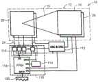
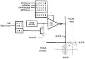
图1中示出了示例光子神经网络系统10的功能框图,并且图2中示出了用于对光子神经网络系统10的图像进行光学处理和卷积的示例光子卷积组装件12的等距视图。利用该光子神经网络系统10的卷积是通过光学傅立叶变换执行的,这与数字空间卷积相比大大提高了速度、分辨率和功率效率,因此与典型的计算卷积和利用计算机算法进行的处理相比,产生并使用神经网络可以以快几个数量级的速度完成,并且功耗要低得多。功耗非常低,这是因为所有的卷积和求和都是完全模拟的、全帧的光子计算。求和是通过在电容式光传感器中构建电荷来完成的,如将在下面解释的,这是模拟过程。传感器是非常低噪声的,并且没有定时或其他瞬态噪声源,因此求和是非常低噪声的过程。光子神经网络10可以接受并处理任何数据(例如,图像、视频、声音、语音模式或通常由卷积神经网络处理的任何事物),并且该光子神经网络10支持所有现有的卷积神经网络架构和训练方法。光子神经网络10还提供了以光速处理的全分辨率的全帧图像并行性,并且具有其中每个数据元素都处于其针对下一阶段的理想位置的架构,因此效率接近100%。根据该描述可以理解其他优点。A functional block diagram of an example photonic
参考图1和图2两者,利用光子卷积组装件12执行对示例光子神经网络系统10的图像的光学处理。本质上,第一传感器-显示设备14投影数据帧(例如,图像或诸如声音、语音模式、视频等之类的其他数据的光学表示)作为经调制的光场15,通过第一傅立叶变换透镜16并通过偏振片18到达放置在透镜16的焦平面中的径向调制器设备20,如将在下面更详细地解释的。基于由支持电子件(在下面更详细地描述)经由电子数据接口22提供给第一传感器-显示设备14的值或信号,来由第一传感器-显示设备14形成由第一传感器-显示设备14投影的数据帧。傅立叶变换透镜16可以是衍射透镜、实心凸透镜或者是可以使用的任何其他形式的傅立叶变换透镜。而且,纤维面板(未示出)可以被放置在透镜16的前方,以在光进入透镜16之前使光准直。Referring to both FIGS. 1 and 2 , optical processing of images of the example photonic
透镜16在焦平面(也称为傅立叶变换平面)处,因此在径向调制器设备20的表面处,将数据帧(例如,图像)变换为其傅立叶当量。径向调制器设备20基于由支持电子件(在下面更详细地描述)经由电子数据接口24加载到径向调制器设备20中的模式(也称为“滤波器”)调制包括数据帧的傅立叶当量的光场15,并且将经调制的数据帧反射到检测结果的第二传感器-显示设备26。包括经调制的数据帧的经反射的光场在从径向调制器设备20到第二传感器-显示设备26的距离中逆傅立叶变换回到空间域中,因此入射在第二传感器-显示设备26上的经调制的数据帧是已经通过径向调制器设备20(即,未被径向调制器设备20滤出的)数据帧的空间域特征。由第二传感器-显示模块26在逐个像素的基础上检测结果,其中入射在每个像素上的光产生与光的强度和光入射在像素上的时间成正比的电荷。可以由径向调制器设备20利用一个或多个滤波器(模式)对从第一传感器-显示设备发射的每个数据帧进行调制。而且,第二传感器-显示设备可以从第一传感器-显示设备14接收由应用于径向调制器设备20中的一个或多个滤波器调制的一个或多个数据帧。因此,针对第二传感器-显示设备26中的每个像素构建的电荷可以是一个或多个数据帧的一个或多个经调制(即,经滤波)的模式的总和,如将在下面更详细地描述的,由此构成由第一传感器-显示设备14投影的一个或多个数据帧的卷积。The
例如,可以由第一传感器-显示设备14顺序地投影一个数据帧,首先以红色,然后以绿色,并且然后以蓝色,并且径向调制器设备20可以将相同或不同的滤波器(模式调制)应用于红色投影、绿色投影和蓝色投影中的每一个。所有这些经调制的数据帧都可以由第二传感器-显示设备26顺序地检测,其中来自那些顺序调制的数据帧中的每一个的光添加到针对每个相应的像素的电荷。然后,针对每个相应的像素的这些电荷被转移到相应的存储器单元,这些存储器单元存储针对每个相应的像素的这些经求和的结果,由此包括在空间域中的数据帧的卷积的存储的像素值,该数据帧由第一传感器-显示设备14投影在空间域中,并由径向调制器设备20中的滤波器在傅立叶变换域中进行卷积。For example, a frame of data may be sequentially projected by the first sensor-
可以针对来自第一传感器-显示设备14的相同数据帧的红色投影、绿色投影和蓝色投影重复该过程,但是利用径向调制器设备20中不同的滤波器,因此来自傅立叶变换域的不同的调制模式由径向调制器设备20反射到第二传感器-显示设备26,由此在第二传感器-显示设备26的存储体中产生另一经求和的结果以及另一经卷积的数据帧的存储的像素值的另一集合。根据由第一传感器-显示设备14针对径向调制器设备20的所有的那些不同的滤波器应用投影的数据帧,在第二传感器-显示设备26中的那些累积的经卷积的数据帧形成3D卷积块。总之,来自第一传感器-显示设备14的数据帧由径向调制器设备20与傅立叶平面中的一系列滤波器进行相乘,并且由第二传感器-显示设备以在第二传感器-显示设备26的存储器中构建3D卷积块的序列进行求和。假定具有足够的存储器容量来存储针对3D卷积块中所有经卷积的数据帧的所有像素值,则可以将任何数量的这种经卷积的数据帧累积到3D卷积块中。该3D卷积块可以被认为是神经网络中的第一级。This process can be repeated for the red, green and blue projections of the same data frame from the first sensor-
对于下一卷积块或下一级,第一传感器-显示设备14和第二传感器-显示设备26交换功能。在第二传感器-显示设备26的存储器中的3D卷积块变为针对下一卷积序列的数据帧。例如,第二传感器-显示设备26的存储器中的3D卷积块中的每个累积的经卷积的数据帧由第二传感器-显示设备26通过第二傅立叶变换透镜28投影到径向调制器设备20,其中该数据帧与滤波器进行相乘并且反射到第一传感器-显示设备14。第一传感器-显示设备14检测一系列这种经卷积的且经求和的数据帧并对其求和,以在第一传感器-显示设备14的存储器中构建下一3D卷积块。For the next convolution block or stage, the first sensor-
该过程周期在图5中示意性地示出。This process cycle is shown schematically in FIG. 5 .
对于任何卷积神经网络架构,可以根据需要多次重复在第一传感器-显示设备14与第二传感器-显示设备26之间反复对数据帧投影的那些卷积过程周期。随着在随后的周期中应用更多的滤波器,可以通过将来自多个像素检测的累积的电荷馈送到一个存储器单元中而不是将来自每个像素检测的累积的电荷馈送到个体存储器单元中来对卷积进行池化,如将在下面更详细地描述的。因此,可以利用示例光子神经网络10来开发具有许多抽象级别的卷积神经网络。For any convolutional neural network architecture, those cycles of the convolution process that repeatedly project the data frame between the first sensor-
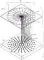
图3中示出了示例径向调制器设备20的正面主视图,并且图4中示出了示例径向调制器设备20的中心部分的透视视图,以及示例径向调制器设备20中的示例片段光调制器的放大的视图。径向调制器设备20具有光学有源区域30,该光学有源区域30包括多个光调制楔形片段32(楔状片段),楔状片段32中的每一个可独立地致动以调制入射在相应的楔状片段32上的光。在图2、图3和图4中示出的示例径向调制器设备20中,楔状片段32被分组为多个楔状扇区34,这些楔状扇区34中的每一个从中心组件36径向向外延伸,并且一起形成径向调制器设备20的光学有源区域30。在图3和图4中,只有楔状片段32和扇区43中的一些标记有那些附图标记,以避免附图中的混乱,但是利用该图示,本领域技术人员将看到并理解所有楔状片段32和楔状扇区34在示例径向调制器设备20中的位置。在图3和图4中示出的示例径向调制器设备20中,楔状片段32被布置为形成圆形的光学有源区域30,但是也可以使用其他形状。A front elevational view of the example
如上面所解释的,在可以激活每个楔状片段32以透射光、阻挡光或在完全透射和阻挡之间调制光的透射的意义上,楔状片段32中的每一个是光学有源的。因此,可以利用一个或多个楔状片段32的任何组合来调制入射在光学有源区域30上的光束或光场。可以设计并构造空间光调制器从而以多种方式调制光。例如,于2006年9月5日授予Rikk Crill的美国专利第7,103,223号说明了在与图2和图3中的径向调制器设备20类似的径向空间光调制器中使用双折射液晶材料来调制楔状片段。Zhang等人的文章“Active metasurfacemodulator with electro-optic polymer using bimodal plasmonic resonance”(Optics Express,Vol.25,No.24,2017年11月17日)描述了具有电光聚合物的电可调金属光栅,其调制光并适用于超薄表面法向应用。在图4中示出了这样的超颖表面(metasurface)光调制器元件40,其被成形以用作示例径向调制器设备20中的光学有源楔状片段32,该超颖表面光调制器元件40包括金属光栅结构42。光栅结构42包括夹在底部金属(例如,Au)层46与相互交错的顶部薄金属(例如,Au)光栅层48之间的电光聚合物44,这些全部构建在衬底50上。光栅44的周期短于光的波长,因此衍射是禁止的。顶部金属层48的厚度大于集肤深度,以消除从入射光L到电光聚合物44中的直接耦合。底部金属层46也具有相同的厚度,使得其用作几乎完美的反射镜。本质上,光L进入超颖表面光调制器元件40的顶部,在电光聚合物44中发生相移(该电光聚合物44通过施加极化电压45而周期性地极化),从底部金属层46反射离开,在其第二次(即,反射)通过期间进一步相移,并且在光的偏振旋转90度的情况下离开顶部表面。示例径向调制器设备20中的其他楔状片段32具有相同类型的光调制器元件40,但是使其尺寸和形状适合并基本上填充每个特定的楔状片段32。中心组件36也可以具有光调制器元件40。As explained above, each of the wedge-shaped
图2-7中示出的并且如上面所描述的示例径向调制器设备20是反射设备,其中入射光由楔状片段32调制并被反射。然而,径向调制器可以替代地是透射设备,其中入射光被调制并透射通过径向调制器。当然,必须重新布置光学组件(例如,传感器-显示设备、透镜和偏振片)的位置,以将光场以适当的序列路由到相应的光学组件,但是本领域技术人员在他们变得熟悉上面描述的示例光子神经网络10之后将知道如何进行这种重新布置。The example
如图3和图4中示出的并且如上面简要解释的,光学有源楔状片段32被分组为多个楔状扇区34,这些楔状扇区34从圆形的中心组件36径向地延伸到光学有源区域30的外围。楔状片段32也以同心环布置在中心组件36周围。除了最里面的同心环之外,楔状片段32的每个同心环的外半径是紧接着相邻的内环的外半径的两倍,这与傅立叶变换中的比例分布相匹配。因此,楔状扇区34中的每个径向向外的在后面的楔状片段32的长度是紧接着在前面的楔状片段32的长度的两倍。对径向调制器如何用作图像的傅立叶变换平面上的滤波器的详细解释可以例如参见于2006年9月5日授予Rikk Crill的美国专利第7,103,223号。足以在这里说,来自空间域中较高空间频率形状含量的光能比来自较低空间频率含量的光能径向向外扩散得更远,而来自较低空间频率含量和来自较高空间频率含量的光能的角度定向和强度则在图像的傅立叶变换中被保留。因此,由放置在距傅立叶变换平面中的经傅立叶变换的图像的中心(光轴)特定角度定向和特定径向距离处的特定的楔状片段32所透射的光能将在投影中逆傅立叶变换回到空间域中,以仅显示原始图像中具有与特定的楔状片段32相同的角度定向的形状内容(特征),并且仅显示该角度定向中具有与这样的光能在傅立叶变换平面中被扩散的径向程度相对应的范围内的空间频率的形状内容(特征)。这些经逆傅立叶变换的特征(形状内容)的光强度(亮度)将与原始图像中具有的那些特征(形状内容)的光强度(亮度)相对应,并且这些经逆傅立叶变换的特征将位于它们在原始图像中所位于的相同位置中。当然,原始图像的光能中所包括的在傅立叶变换平面中由特定的楔状片段32阻挡并且不被透射的形状内容(特征)将在回到空间域中的经逆傅立叶变换的图像中丢失。而且,光能中所包括的仅在傅立叶变换平面中由特定的楔状片段32部分地阻挡并因此部分地透射的形状内容(特征)将如上面所解释的以相同的角度定向和特定的空间频率逆傅立叶变换回到空间域,但强度(亮度)降低。因此,如上面所解释的并且如将在下面更详细地解释的,回到空间域的经逆傅立叶变换的图像是在构建针对如图5中示出的神经网络的3D卷积块时被检测到并使用的卷积图像,其中原始图像的形状内容(特征)中的一些以完全或部分强度(亮度)在经逆傅立叶变换的图像中被保留,并且其中形状内容(特征)中的一些在经逆傅立叶变换的图像中被完全删除。As shown in FIGS. 3 and 4 and as briefly explained above, the optically
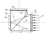
因此,参考图5,第一滤波器54经由数据接口24加载到径向调制器设备20中,该第一滤波器54将楔状片段32设置为以由第一滤波器54设置的模式完全地或部分地透射光或者阻挡光。包括例如一堆LEGOTM玩具积木52的图像的第一数据帧50经由数据接口22加载到第一传感器-显示设备14中,因此将第一传感器-显示设备14中的显示组件(图5中未显示)设置为显示包括LEGOTM玩具积木52的图像的数据帧,如图5中可以看出的。激光照明13指向第一传感器-显示设备14,该激光照明13实质上把包括LEGOTM玩具积木的图像的数据帧50的光通过第一傅立叶变换透镜16并通过偏振片18投向径向调制器设备20,该径向调制器设备20放置在傅立叶变换平面中距第一傅立叶变换透镜16焦距F1处,即,在第一傅立叶变换透镜16的焦平面中,也如图6中示意性地示出的。傅立叶变换透镜16将包括图像50的光场15聚焦到径向调制器设备20的表面上的焦点处。包括LEGOTM玩具积木52的图像的数据帧50通过径向调制器设备20的楔状片段32在傅立叶变换域中利用滤波器进行卷积,该滤波器完全地或部分地反射一些光或阻挡图像中包括的一些光,如上面所解释的。楔状片段32相移,因此旋转经反射的光的偏振,使得由径向调制器设备20反射的光由偏振片18反射到第二传感器-显示设备26,如由经反射的光场56所指示的。因此,如上面所解释的,在入射在第二传感器-显示设备26上的经卷积的图像中,LEGOTM玩具积木52的图像的原始数据帧50的一些形状内容(特征)丢失或强度减弱,即,被滤出,如图5中示出的。经卷积的数据帧(图像)在第二传感器-显示设备26处被检测到,并且在第二传感器-显示设备26中与一些随后的经卷积的图像进行求和以形成第一经卷积的且经求和的数据帧(图像)58。可以将该第一经卷积的且经求和的数据帧(图像)58转移到存储体中,以用于与随后的经卷积的且经求和的数据帧(图像)进行累积,从而构建3D卷积块64,如图5中示意性地示出的。Thus, with reference to FIG. 5 , a first filter 54 is loaded into the
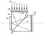
然后,第二传感器-显示设备26和第一传感器-显示设备14如上面所解释地交换角色,使得第二传感器-显示设备26进入显示模式,并且第一传感器-显示设备14进入传感器模式。在第二传感器-显示设备26在显示模式下的情况下,该第一经卷积的且经求和的数据帧(图像)58然后由第二传感器-显示设备26投影回到径向调制器设备20,如图7中示意性地示出的,第一经卷积的且经求和的数据帧(图像)58在该径向调制器设备20中利用附加的滤波器进行卷积,并且然后由径向调制器设备20反射回第一传感器-显示设备14。该角色交换在图7中示意性地示出,其中第二传感器-显示设备26切换到显示模式,并且第一传感器-显示设备14切换到传感器模式。在显示模式下,第二传感器-显示设备26的显示组件被编程为显示第一经卷积的且经求和的数据帧(图像)58。因此,在第二传感器-显示设备26上的激光照明60把第一经卷积的且经求和的数据帧(图像)58的光通过第二傅立叶变换透镜28沿着第二光轴62投向偏振片18,该偏振片18将光场64沿着第一光轴61反射到径向调制器设备20。第二傅立叶变换透镜28与径向调制器设备20之间的沿着第二光轴62和第一光轴61的光学距离等于第二傅立叶变换透镜28的焦距。因此,在傅立叶变换平面中的径向调制器设备20处的光场64是第一经卷积的且经求和的数据帧(图像)58的傅立叶变换。径向调制器设备20将滤波器应用于该第一经卷积的且经求和的数据帧的傅立叶变换,以向数据帧提供第二卷积,并且如上面所解释的在相移的情况下反射该数据帧,以然后沿第一光轴61传播到第一传感器-显示设备14。如上面所解释的现在处于检测器的交换角色中的第一传感器-显示设备14检测由径向调制器设备20应用的滤波器卷积的数据帧(图像)。然后,由第一传感器-显示设备14检测到的经卷积的数据帧(图像)由第一传感器-显示设备14与第一传感器-检测器设备14随后检测到的一些其他经卷积的数据帧(图像)进行求和,并且将这种经卷积的且经求和的数据帧(图像)转移到存储体,并且用于构建第二3D卷积块66,这在图7中示意性地示出。The second sensor-
然后,再次交换第一传感器-显示设备14和第二传感器-显示设备26的角色,并且由第一传感器-显示设备14感测并求和的经卷积的且经求和的数据帧然后通过系统以如上面所描述的相同的方式投影回去以进行以下操作:由径向调制器设备20进行卷积并且然后由第二传感器-显示设备26检测并求和以继续构建第一3D卷积块64;以及通过系统发送回去以利用附加滤波器进行卷积并且求和以继续构建第二3D卷积块66。该过程根据需要循环多次以构建越来越深的卷积,或者直到推理神经网络完成为止。The roles of the first sensor-
第一传感器-显示设备14和第二传感器-显示设备26可以各自具有存储体(如在下面更详细解释的),以用于存储其接收到的并与随后接收到的经卷积的数据帧(图像)进行求和以构建3D卷积块64、66和随后的卷积块的经卷积的数据帧(图像)。因此,除了加载到系统中的第一数据帧(图像)之外,输入数据帧可以始终驻留在来自先前的卷积周期的传感器-显示设备14、26中的一个的存储体中。一系列滤波器68与由相应的第一传感器-显示设备14和第二传感器-显示设备26显示数据帧(图像)同步地被加载到径向调制器设备20中,以用于利用滤波器对数据帧(图像)进行卷积。The first sensor-
除了已经在傅立叶变换域中光学地计算之外,来自该光子神经网络系统10的卷积与由传统数字方法计算出的卷积相同。然而,利用其中每个数据元素都处于其针对周期的下一卷积阶段的理想位置的架构以光速处理的任何分辨率的全帧并行性(如在下面更详细地解释的)的效率接近100%,因此如上面所描述的以及在下面更详细地描述的,利用示例光子神经网络系统10构建卷积块提供了比由传统数字方法计算出的卷积更高的功率和速度。The convolution from the photonic
如上面所解释的,第一传感器-显示设备14和第二传感器-显示设备26中的每一个都具有在逐个像素的基础上的光检测能力和图像显示能力两者。在该示例光子神经网络系统10中,第一传感器-显示设备14和第二传感器显示设备26具有本质上彼此相同的组件和结构,因此下面主要参考第一传感器-显示设备14来描述这些设备的细节,但应理解,这些细节也表示第二传感器-显示设备26。因此,在以下描述中,有时将第一传感器-显示设备14简称为传感器-显示设备14。示例传感器-显示设备14的功能框图在图8中示出,并且包括发射-接收模块82的阵列80,发射-接收模块82中的每一个具有光透射和光检测元件以及存储体,如将在下面更详细地描述的。提供用于阵列80中的发射-接收模块82的行控件和列控件以及到外部控制电路(图8中未示出)的混合的模拟和数字接口24,以用于输入和输出数据,这将在下面更详细地描述。图9中示意性地示出的阵列80的放大的部分示出了阵列80中的示例发射-接收模块82,并且图10中示出了示例发射-接收模块82的进一步放大的示意性表示。示例发射-接收模块82中的每一个包括微型光发射器元件84和微型光检测器(传感器)元件86两者,这些元件对于发射-接收模块足够小并且彼此足够接近,以在具有足够分辨率的图像或数据帧的基本相同的像素位置处高效地用作光的发射器和光的接收器,以用于操作有用的神经网络,例如,神经网络结果与来自典型的计算卷积并且利用计算机算法处理的神经网络结果至少一样有用。例如,对于其中示例光子神经网络系统10与来自典型的计算卷积并且利用计算机算法处理的神经网络结果一样有用的神经网络结果,微型光发射器元件84和微型光检测器元件86可以彼此偏移不大于40微米,并且两者都在具有不大于160平方微米的面积的发射-接收模块82内适合。As explained above, the first sensor-
如图10中最佳看出的,除了光发射器元件84和光传感器或检测器元件86之外,示例发射-接收模块82还具有调制器驱动器88、存储体90、存储器接口92、模拟和数字控制元件94、用于与阵列80中相邻的发射-接收模块82进行池化连接的池化连接96、池化控制元件98以及感测放大器100。在显示模式下,例如,当第一传感器-显示设备如上面所解释地将数据帧(图像)投影到径向调制器20时,将激光照明指向发射-接收模块82的背面,如图2、图5和图6中示出的。第一数据帧(图像)由用于数据帧(图像)的每个像素的像素值组成。这些像素值以将在激光照明的光场中创建第一数据帧(图像)的模式被馈送到阵列80的相应的发射-接收模块82中。对于如图10中示出的发射-接收模块82中的单独一个发射-接收模块,像素值被馈送到模拟和数字控制元件94中,该模拟和数字控制元件94将像素值移位到调制驱动器88。调制驱动器88根据像素值调制光发射器元件84上的电压,从而以这样的方式调制入射在光发射器元件84上的激光照明:在其他光发射器元件84正在发射光的相应的像素的同时发射激光照明的像素,这些像素一起将数据帧(图像)施加到通过阵列80发射的激光场上。在第一数据帧(图像)由第一传感器-显示设备14发射并且经卷积的数据帧(图像)被引导回到该第一传感器-显示设备14之后,包括该经卷积的数据帧(图像)的光场入射在第一传感器-显示设备14的阵列80中的所有发射-接收模块82的传感器86上。因此,阵列中每个发射-接收模块82上的传感器86检测入射光场的像素,因此检测入射光场包括的数据帧(图像)的像素。本领域技术人员理解光传感器(例如,电荷耦合设备(CCD))如何构成并运作,并且这种光传感器或类似的光传感器可以用于传感器86。本质上,每个光传感器都具有光感测光电二极管或电容式组件,其通过吸收光子中的能量中的大部分并且创建与入射光强度成正比的电荷并且在电容式组件中累积电荷来响应光的入射光子。光入射在传感器上的时间越长,电容式组件中累积的电荷就越多。因此,入射在每个传感器86上的光能的像素使电荷构建在该传感器86中,并且电荷的幅度与该像素中的入射光的强度和该像素中的光入射在传感器86上的时间成正比。As best seen in FIG. 10, in addition to
如上面所解释的,如果将一系列的经卷积的数据帧(图像)发射到传感器显示设备14并由传感器显示设备14接收,则包括顺序的数据帧(图像)的顺序的光场的光能(光子)会在传感器86中带来电荷,因此来自由个体传感器86感测到的顺序的光场的光场能量的顺序的像素可以被累积(即,被添加)到该个体传感器86的电容式组件,由此导致传感器86中累积的电荷,这些电荷是来自在该特定像素位置处的光场的序列的光能的总和。因此,由传感器-显示设备14的发射-接收模块82的阵列80在逐个像素的基础上感测由传感器-显示设备14接收到的经卷积的数据帧(图像)的序列并对其求和。然后,如上面所解释的,当规定数量的个体经卷积的数据帧(图像)已经被接收并求和时,每个个体发射-接收模块82的传感器86中的累积的(经求和的)电荷被移位到该个体发射-接收模块82的存储体90中。将传感器86中的累积的(经求和的)电荷移位到存储体90中的相同操作在阵列90中的所有发射-接收模块82中同时发生。因此,在执行该移位操作时,发射-接收模块92的阵列90已经将由对输入数据帧(图像)的卷积的该系列或序列进行的卷积和求和产生的完整经卷积的且经求和的数据帧(图像)存储在发射-接收模块92的个体存储体90中。参考图10,针对在该特定的发射-接收模块82的像素位置处的该第一经卷积的且经求和的数据帧(图像)的像素值从传感器86移位到第一存储器单元102中。因此,阵列80的所有发射-接收模块82的存储体90中的所有第一存储器单元102的复合物包括在逐个像素的基础上的经卷积的且经求和的数据帧(图像)。As explained above, if a series of convoluted data frames (images) are transmitted to and received by the
然后,当如上面所描述地对数据帧(图像)的随后的第二系列或序列进行卷积并求和时,随着来自第一经卷积的且经求和的数据帧(图像)的像素的电荷同时被移位到存储器90的第二存储器单元104,在传感器86中的针对所产生的第二经卷积的且经求和的数据帧(图像)的像素的累积的电荷被移位到第一存储器单元102中。本领域技术人员理解如何制造并操作这样的移位寄存器存储器,因此出于该解释的目的,详细描述不是必要的。该相同的过程在阵列80中的其他发射-接收模块82中同时发生。因此,阵列80的所有发射-接收模块82的存储体90中的所有第一存储器单元102和第二存储器单元104的复合物包括在逐个像素的基础上的第一经卷积的且经求和的数据帧(图像)和第二经卷积的且经求和的数据帧(图像)。Then, when the subsequent second series or sequence of data frames (images) are convolved and summed as described above, with the The charges of the pixels are simultaneously shifted to the
如上面所描述的,随着越来越多的数据帧(图像)的随后的系列或序列被卷积并求和,这种顺序的经卷积的且经求和的数据帧(图像)的经求和的像素值按序列移位到第一存储器单元102中,而每个在前面的像素值沿着存储体90的存储器单元移位地更远,并且如上面所解释的,该过程在阵列80的所有发射-接收模块82中同时发生。因此,来自卷积和求和的所有系列或序列的所有这种经卷积的且经求和的数据帧(图像)在逐个像素的基础上存储在发射-接收模块82的阵列80中的存储体90的存储器单元中。这种经卷积的且经求和的数据帧(图像)中的每一个有时被称为卷积,因此发射-接收模块82的阵列80可以在逐个像素的基础上保持如发射-接收模块82的个体存储体90中存在的个体存储器单元一样多的卷积。例如,图9和图10中示意性地示出的示例发射-接收模块82各自具有由64个个体存储器单元102、104、……、n组成的存储体90。因此,在全分辨率逐个像素的基础上,发射-接收模块82的示例阵列80可以保持如数据帧(图像)的64个卷积一样多的卷积。当将发射-接收模块82(参见图1)中的光发射器元件84和光传感器元件86与相邻的发射-接收模块82的光发射器元件84和光传感器元件86池化到一起时,如在下面更详细地描述的,池化的组中的所有光发射器元件84和光传感器元件86对于数据帧(图像)的粗略的表示显示相同的亮度。在这样的池化条件下,池化的组中的发射-接收模块82的存储体90可以顺序使用,以保存针对发射-接收模块82的整个池化的组的感测到的且经求和的结果,并且由此增加有效存储器容量和深度。例如,如果各自具有包括64个存储器单元的存储体90的发射-接收模块82被池化为5×5个组,即,每组二十五个发射-接收模块82,则每个组的有效存储器容量或深度是1600个存储器单元(64×25=1600)。因此,可以将顺序的经卷积的且经求和的数据帧(图像)首先馈送到组中的发射-接收模块82中的一个中,直到该发射-接收模块82的存储体90被填充为止,并且然后可以将更多的顺序的经卷积的且经求和的数据帧(图像)馈送到组中的第二发射-接收模块82中,直到该第二发射-接收设备82的存储体90也被填充为止,并且然后继续顺序地填充该组中其余的发射-接收模块82的相应的存储体90。如果组中的所有发射-接收模块82的存储体90都被填充,则存储器中的卷积的该块的深度将为1600。将阵列80中的发射-接收模块82的存储器90中的卷积聚合在一起是卷积块,例如,图5中示意性地示出的3D卷积块65。当在阵列中针对最后一个3D卷积块累积了期望数量的这种卷积时,可以在逐个像素的基础上从存储体90中读出这些卷积,以供传感器-显示设备14在处理的结束处通过电子数据接口22发送回去以输出神经网络结果。As described above, as more and more subsequent series or sequences of data frames (images) are convolved and summed, the convolved and summed data frames (images) of this order have The summed pixel values are shifted in sequence into the first memory cell 102, while each preceding pixel value is shifted further along the memory cells of the
然而,重要的是重申,在利用示例光子神经网络系统10重复地对数据帧进行进一步卷积和求和的深度学习过程期间,针对最新形成的卷积块的像素值仍驻留在个体发射-接收模块82中的个体存储体90的存储器单元中。因此,当传感器-显示设备14从传感器模式(其中卷积块在发射-接收模块82的存储器90中累积)切换到显示模式(其中卷积块通过系统10的光学组件被发送回去以用于更深的卷积处理)时,针对包括卷积块的经卷积的且经求和的数据帧(图像)中的每一个的像素值都可以直接从存储器90的存储器单元102、104、……、n读取(移位)到调制器驱动器88,而不进行任何进一步的处理以及将数据转移到外部计算机处理、存储器以及其他组件或功能中或从其中转移出来。相反,当从传感器模式切换到显示模式时,包括卷积块的个体数据帧(图像)的像素值从存储器90顺序地直接读取(移位)到调制驱动器88,该调制驱动器88驱动光发射器元件84来以这样的方式调制入射在发射-接收模块82上的激光:将要在该卷积周期中进一步卷积的数据帧(图像)的像素值写入(施加)到光场中。因此,由于将阵列80中的所有发射-接收模块82同时切换到显示模式,并且将这些模块中的每一个中的像素值写入(施加)到激光场中,所以在由传感器-显示设备14发送的光场中的这些像素值的复合物复制了在阵列80中的发射-接收模块82的存储体90中经求和的且存储的先前经卷积的数据帧(图像)。然后,将包括先前经卷积的且经求和的数据帧(图像)的光场通过傅立叶变换透镜16投影到径向调制器20,以利用滤波器在傅立叶变换平面中进一步卷积,并且该光场然后在另一(例如,第二)传感器-显示设备26处进行检测,如上面所解释的。However, it is important to reiterate that during the deep learning process of further convolving and summing the data frame iteratively with the example photonic
还如上面所解释的,这些卷积和求和过程利用许多滤波器通过许多周期再三重复。而且,第一传感器-显示设备14和第二传感器-显示设备在它们相应的光轴61、62(参见图2、图6和图7)上以这样的方式对齐:在第一传感器-显示设备14中的发射-接收模块82与在第二传感器-显示设备26中的对应的发射-接收模块82在光学上对齐,使得在第一传感器-显示设备14和第二传感器-显示设备26的相应的阵列80之间(包括在对应的发射-接收模块之间)存在完全的光学对准。因此,示例光子神经网络10以光速执行全帧、全分辨率、完全平行的卷积。如将在下面更详细地描述的,诸如增益、阈值(ReLU)、最大或平均池化以及其他功能之类的其他效果是与专用电路同时执行的,并且这些效果表示没有附加的时间延迟。实际上,可以容纳任何卷积神经网络架构,包括例如VGG16或Inception-Resnet-v2。所有处理完全在传感器-显示设备14、26上完成,而不将数据帧(图像)重新定位到这些设备中以及重新定位到这些设备外。在推理操作中,用户应用仅需加载图像并在几微秒后接受结果。As also explained above, these convolution and summation processes are repeated over and over again through many cycles using many filters. Furthermore, the first sensor-
在发射-接收模块82中的微型光发射器元件84可以是发出或调制光的任何光调制器设备。对上面描述的示例光子神经网络系统10的描述包括光发射器元件84,该光发射器元件84通过允许或禁止光透射通过光发射器元件来调制入射在光发射器元件背面的激光。然而,如本领域技术人员一旦变得理解上面描述的示例光子神经网络就能够理解的,光发射器元件84可以由反射光调制器设备代替,该反射光调制器设备调制入射光并进行反射,这将要求激光照明入射在光从其反射的光发射器元件的相同表面上,并且将要求重新布置光学元件。作为另一替代方案,光发射器元件84可以由光发射管代替,这将消除对照在调制器背面并穿过调制器的激光场的需要。The miniature
图11中示出了一个示例光发射器元件84,其类似于图4中示出的并且在上面描述的超颖表面光调制器元件40来调制入射光的相位。然而,由于图11中的该示例光发射器元件84是光透射元件而不是图4中的光反射元件,因此底部金属层46在光栅结构之间是有空隙的,以像顶部电极48那样相互交错,使得入射光L被电光聚合物44进行相位调制以由电光聚合物44阻挡或者被允许穿过光栅结构42。衬底50对于光L是透明的。极化电压45由发射-接收模块82的调制器驱动器88根据要施加在光场L中的像素值驱动,如上面所解释的。这种透射光调制器的更多细节可以参见Kosugi等人的文章“Surface-normal electro-optic-polymer modulator with silicon subwavelength grating”(IEICE ElectronicsExpress,Vol.13,No.17,第1-9页,2016年9月10日)。An example
发射-接收器模块82的背面一侧具有覆盖背表面的不透明覆盖物或掩模(未示出),以阻止发射-接收模块82的背面上的激光照明透射通过除了允许光到达并穿过光发射器元件84的孔径之外的发射-接收模块82。包括傅立叶变换透镜16和用于使傅立叶变换透镜16前方的光准直的纤维面板在内的光学组件可以结合到第一传感器-显示设备14的前方。同样地,可以将傅立叶变换透镜28和纤维面板结合到第二传感器-显示设备26的前方。The back side of the transmitter-
现在参考图1,除了光子卷积组装件12的第一传感器-显示设备14和第二传感器-显示设备26以及径向调制器设备20之外,示例光子神经网络系统10还包括外部控制组件,包括例如:(i)电路块110,其实现脉冲输出以驱动径向调制器设备20;(ii)高速模拟-数字电路块112,通过该高速模拟-数字电路块112将数字数据加载到第一传感器-显示设备14和第二传感器-显示设备26以及从其接收数字数据;高带宽存储器(HBM2)114;以及现场可编程门阵列(FPGA)116,其为用于其他系统组件的基本控制和接口设备。HBM2 114为滤波器、状态机步骤和图像数据提供存储。电路块110、HBM2 114和FPGA 116在多芯片模块(MCM)118上,并且到系统10的用户接口名义上通过PCI-快速总线120。Referring now to FIG. 1, the example photonic
在图12中示出了现场可编程门阵列(FPGA)116与第一传感器-显示设备14之间的示例系统接口122的功能框图。图12中的功能框图也表示了在FPGA 116与第二传感器-显示设备26之间的系统接口。为了附图中的方便和简洁起见,在针对电路块110的附图和相关联的描述中有时使用任意术语“RedFive”,并且针对传感器-显示设备14、26有时使用任意术语“Sensay”(传感器(sensor)和显示器(display)的缩写)。还为了方便和简洁起见,有时将发射-接收模块82称为“trixel”(“trixel”是“发射-接收像素(transmit-receive pixel)”的缩写)。A functional block diagram of an
RedFive中的一些用于生成模拟数据以加载Sensay存储器90。由于存储器模块(HBM2)114是由FPGA 116管理的状态机源,因此这些RedFive通过HBM2 114接合。由于FPGA116用于控制反馈回路,因此模拟和数字输入/输出(I/O)通过该FPGA 116接合。一些未使用的位作为用于同步的状态标志被包装回到FPGA 116。Sensay数字I/O使用与RedFive中的一些相同的存储器线,但它们不能被同时访问,因此存储器线的这种双重使用不是冲突的。而且,来自RedFive的传出模拟线中的一些作为到ADC的传入模拟线被共享。用于读取数据并将数据传递给FPGA 116的ADC数量取决于实现方式。Some of the RedFives are used to generate simulated data to load the
图13中示出了Sensay外部接口的功能框图。在图13中,“Sx”用于前面的“SensayA”14或“SensayB”26(在讨论系统时用于区分与Sensay 14、Sensay 26中的任一个相关联的信号)。图8中的数字输入线可以分组为三个一般类别。行控件和列控件在Sensay中加载一组锁存器(参见图14)。全局控制线具有各种功能,这些功能中的每一个将在使用的上下文中描述。全局线可以沿着行或列路由。全局控制线路由到所有的发射-接收模块(trixel)82,并且对于特定的列或行不是唯一的。A functional block diagram of the Sensay external interface is shown in FIG. 13 . In Figure 13, "Sx" is used for the preceding "SensayA" 14 or "SensayB" 26 (used to distinguish signals associated with either of
SxPeakreset重置用于外部增益控制的模拟峰值保持电路。该信号是异步的,但是为了避免数据争用,应仅在使SxFreeze有效时使该信号有效(1)。SxPeakreset resets the analog peak hold circuit for external gain control. This signal is asynchronous, but to avoid data races, it should only be asserted when SxFreeze is asserted (1).
SxSnsreset将传感器重置为模拟SxLevel线的电平。传感器被设计为累积电荷,因此这些传感器需要这种机制来降至预设电平。注意,该重置可以用作全局偏置,以预设传感器电荷电平(并因此在下一次传递时预设调制器电平)。SxSnsreset resets the sensor to the level of the analog SxLevel line. Sensors are designed to accumulate charge, so these sensors need this mechanism to drop to a preset level. Note that this reset can be used as a global bias to preset the sensor charge level (and thus the modulator level on the next pass).
SxPoolmode确定池化中的平均(1)操作或最大(0)操作。SxPoolmode determines the average (1) operations or maximum (0) operations in pooling.
SxFreeze启用和禁用全局存储器访问。如果使SxFreeze有效(1),则所有trixel存储器驱动器都被设置为安全状态,并且不允许进行任何存储器访问或移位。SxFreeze在配置其他控制线时使用,以防止在安排线之前污染数据。在下面的解释中,并不总是提到SxFreeze的功能,但是其动作总是支配的。SxFreeze enables and disables global memory access. If SxFreeze is enabled (1), all trixel memory drives are set to a safe state and no memory accesses or shifts are allowed. SxFreeze is used when configuring other control lines to prevent contamination of data before the line is scheduled. In the explanations below, the functionality of SxFreeze is not always mentioned, but its actions always govern.
SxRWDir确定是读取还是写入启用的存储器。如果设置为“1”,则将数据写入存储器,并且如果设置为“0”,则从存储器读取数据。SxRWDir还门控传感器(光检测器元件)86和调制器(光发射器元件)84的操作。SxRWDir表示调制器模式(0)或传感器模式(1)。SxRWDir determines whether to read or write enabled memory. If set to '1', data is written to memory, and if set to '0', data is read from memory. SxRWDir also gates the operation of sensor (light detector element) 86 and modulator (light emitter element) 84 . SxRWDir represents modulator mode (0) or sensor mode (1).
SxFlagRD、SxFlagWR和SxFlagRST控制用于语义标记的数字标志存储器。SxFlagRST是针对所有标志存储器的全局地址重置。SxFlagRD和SxFlagWR控制存储器访问。SxFlagRD, SxFlagWR, and SxFlagRST control the digital flag memory used for semantic flagging. SxFlagRST is a global address reset for all flag memories. SxFlagRD and SxFlagWR control memory access.
SxShift0、SxShiftl、SxShift2以三相序列从外部驱动,以仅在寻址的trixel(发射-接收模块)82处以顺时针方向或逆时针方向移动移位寄存器存储器90电荷。如果trixel是未寻址的,则其存储器驱动线被强制进入安全状态,并且存储器电荷不受影响。SxShift0, SxShift1, SxShift2 are externally driven in a three-phase sequence to move
SxExtemal确定SxAnalog和SxData线是活动的(1)还是数据移动和访问仅是内部的(0)。SxExtemal determines whether the SxAnalog and SxData lines are active (1) or if data movement and access are internal only (0).
考虑这些信号的四种组合:Consider four combinations of these signals:
图像加载:SxFreeze=0,SxRWDir=1,SxExternal=1。这表示在寻址的trixel 82处的任何存储器单元将从外部SxAnalog线获取数据,并经由内部SxData线将电压放置在(多个)trixel存储体90中。由于存在120条SxAnalog线,因此该动作可以高达120宽。对于其中120宽设置的DAC不适合的实现方式,可以将这些线在外部连接成组,并且可以仅通过按序列启用MEMR线来容纳更窄的访问。不管实现的外部行宽度如何,为了避免争用,典型地一次仅启用一条MEMC线(但是如果需要,可以一次将相同的DAC值发送到整行)。Image loading: SxFreeze=0, SxRWDir=1, SxExternal=1. This means that any memory cell at the addressed
结果保存:SxFreeze=0,SxRWDir=0,SxExternal=1。这表示在寻址的trixel 82处的任何存储器单元将向外部SxAnalog线发送数据,以用于与外部ADC进行转换。再次强调,这可以高达128宽,但是可以在不对Sensay进行设计改变的情况下容纳更窄的实现方式。不管实现的外部行宽度如何,为了避免争用,一次仅启用一个MEMC(为了避免数据争用,这对于读取不是可选的)。The result is saved: SxFreeze=0, SxRWDir=0, SxExternal=1. This means that any memory cell at the addressed
传感器模式:SxFreeze=0,SxRWDir=1,SxExternal=0。这表示在寻址的trixel82处的任何存储器单元将(经由池化链,这将在下面描述)从传感器86获取数据,并且与SxShift0、SxShift1、SxShift2结合,在将现有的电压移位作为存储器值的移位寄存器集合时将电压保存为新的存储器电荷。Sensor Mode: SxFreeze=0, SxRWDir=1, SxExternal=0. This means that any memory cell at the addressed
调制器模式:SxFreeze=0,SxRWDir=0,SxExternal=0。这表示在寻址的trixel82处的任何存储器单元将(经由池化链)把数据发送到调制器(光发射器元件)84,并且与SxShift0、SxShift1、SxShift2结合,将现有的电压移位作为存储器电荷的移位寄存器集合。存储器读取是非破坏性的。Modulator mode: SxFreeze=0, SxRWDir=0, SxExternal=0. This means that any memory cell at the addressed
在图14中示意性地示出了用于trixel(发射-接收模块)82的示例行和列控制线寄存器。在该示例中,行和列控制线寄存器包括235个单独寻址的静态64位锁存器,其被布置为每个trixel具有五条行线和五条列线。这些输出总是活动的,并且在上电时置零。由每个trixel 82使用这些行和列控制线用于相对于其邻居配置自身以用于其功能。通过在SxControl处使数据有效、在SxAddr处设置8位地址并向SxLatch施加脉冲,对锁存器中的每一个进行单独寻址。Example row and column control line registers for trixel (transmit-receive module) 82 are shown schematically in FIG. 14 . In this example, the row and column control line registers include 235 individually addressed static 64-bit latches arranged with five row and five column lines per trixel. These outputs are always active and are set to zero on power-up. These row and column control lines are used by each
当使trixel的MEMR和MEMC两者都有效时,trixel的存储器90被认为是“寻址的”。类似地,当使trixel的OPTC和OPTR两者都有效时,其光学传感器是“寻址的”。当使trixel的ENBR和ENBC都失效时,杂项trixel82功能被禁用。为了完全禁用trixel 82,同样地使其MEMR、MEMC、OPTR、OPTC、FLAGR和FLAGC失效。A trixel's
池化边界线86(POOLC和POOLR)影响trixel 82的整个列和行,并且定义超级trixel的边界,如将在下面更详细地描述的。始终启用最右边和最底端的线,因此只有1079条POOLR线和1919条POOLC线。未连接在64位锁存器中未使用的线。Pooling boundary lines 86 (POOLC and POOLR) affect the entire column and row of
*_SL线和*_SR线在上升沿向左或向右移位它们相应的寄存器。The *_SL and *_SR lines shift their corresponding registers left or right on rising edges.
SxReLU1和SxReLU2(图13)由外部DAC驱动。它们对于所有trixel82是全局的,并且应用传感器86读取值以消除弱信息。SxLevel(图13)也由外部DAC驱动。该SxLevel由所有trixel传感器86使用作为预设电平,并且还将SxLevel求和到调制器驱动88电平中,在其中将SxLevel用作相位偏移。如上面所解释的,由于sensay(传感器-显示设备)14或26在任何时刻都处于传感器模式或调制器(发射)模式,因此不存在争用。SxPeak(图13)模拟输出信号是来自所有trixel(发射-接收模块)82的信号。如在下面更详细地描述的,每个trixel存储器单元将其最高值传递给公共迹线。该迹线的值表示自上次使SxPeakreset有效以来整个trixel阵列看到的最高全局值。这由外部电路用于系统增益和归一化。SxReLU1 and SxReLU2 (Figure 13) are driven by external DACs. They are global to all trixels 82 and
图15中示意性地示出了示例模拟接口。SxAnalog线是120条迹线,每条迹线连接九个相邻的SxData行。换言之,内部SxData0000行迹线至SxData0008行迹线都连接到输出引脚SxAnalog000。SxData0009行迹线至SxData0017行迹线都连接到输出引脚SxAnalog001等。每个SxAnalog引脚都硬连线至九条内部SxData迹线。一次将仅允许一个trixel存储体90来驱动或感测其本地迹线(由外部控制器强制执行)。如果使TMS有效,则所有SxAnalog线和SxData线都连接在一起。An example analog interface is schematically shown in FIG. 15 . The SxAnalog lines are 120 traces, each connecting nine adjacent SxData lines. In other words, the internal SxData0000 row traces to the SxData0008 row traces are all connected to the output pin SxAnalog000. The SxData0009 row traces to the SxData0017 row traces are all connected to the output pins SxAnalog001 and so on. Each SxAnalog pin is hardwired to nine internal SxData traces. Only one
可以注意的是,如上面所讨论的,由于控制线是单独可控的,因此可以仅通过将这些线一起连接到Sensay(传感器-显示设备)外部,并仅启用适当的trixel 82以匹配架构,实现从1至120宽的任何尺寸的输入或输出方案。接口越宽,则加载和卸载操作就越快,但是要求越多的外部电路。这在不改变设计的情况下允许高度定制。It may be noted that, as discussed above, since the control wires are individually controllable, it is possible to simply connect these wires together externally to the Sensay (sensor-display device) and only enable the
在示例光子神经网络系统10中的Sensay(传感器-显示设备)14、26架构在池化链周围构建。如图9、图10和图16中示出的,阵列80中的发射-接收模块(trixel)82中的每一个具有沿着其边缘中的两个(例如,在那些图9、图10和图16在纸上被定向时沿着右边缘和底边缘)的池化边界线96。所有传感器、调制器、存储器读取或存储器写入访问都使用池化链以在trixel(传感器-显示设备)82内以及之间传递模拟数据。池化边界线96的功能是将附近的发射-接收模块(trixel)82从池化链连接或断开连接,从而创建超级trixel或“岛”。在图17中的连接的放大的示意图中,在trixel 82的阵列80中的假设位置nnnn,mmmm处,示出了到相应的相邻trixel 82的边界线96的池化链电路连接。如果POOLC=0,则针对整个列的所有东西trixel池化链连接是开放的。如果POOLR=0,则针对整个行的所有南北trixel池化链连接是开放的。所有其他trixel池化链连接仍然闭合。这种池化结构的效果是创建连接的池化链线的岛。在超级trixel岛上的所有trixel共享该链,该链本质上是单个低阻抗“迹线”。如果使POOLR有效,则连接该trixel的池化链的晶体管将导通,从而将池化链与下一行的在其南部的trixel 82连接起来。如果使POOLC有效,则将池化链与东部的trixel 82连接起来。The Sensay (sensor-display) 14, 26 architecture in the example photonic
如上面所提到的,发射-接收模块(trixel)82中的每一个中的存储体90本质上是移位寄存器,并且移位寄存器设计和技术对本领域技术人员是很好理解的并且可容易获得。图18示出了模拟存储器移位驱动器方案。在寻址的(使MEMC和MEMR有效)且未冻结的(使SxFreeze失效)的情况下,SxShift0、SxShiftl、SxShift2的任何组合将仅传播到实际驱动模拟存储器单元移位板的输出(MemShift0、MemShiftl、MemShift2)。如果对于trixel使MEMC或MEMR失效,或者如果使SxFreeze有效,则模拟存储器驱动器将自动地置于安全状态(MemShift0、MemShift01、MemShift02=010)。As mentioned above, the
图19是用于存储体90(图10)的示例模拟存储器读取接口的示意图。可以读取存储器并且经由内部SxData线将模拟数据路由到外部SxAnalog接口,或者可以通过最大(二极管)电路路径或平均(电阻器)电路路径将模拟数据发送到池化链126(如果该模拟数据大于SxReLU,否则将其置零)。从模拟存储器读取的未经修改的值还用于对二极管隔离的电容器(采样保持电路)进行充电,最终驱动针对整个传感器-显示设备(sensay)14、26的SxPeak值(针对系统增益控制在外部使用)。这些模式的示例在图20-24中示意性地示出。图20示出了对池化链平均的trixel模拟存储器读取。图21示出了对池化链最大的trixel模拟存储器读取。图22示出了到外部数据线的模拟存储器读取。图23示出了trixel模拟存储器峰值保存。图24示出了模拟存储器峰值重置。19 is a schematic diagram of an example analog memory read interface for bank 90 (FIG. 10). The memory can be read and the analog data routed to the external SxAnalog interface via the internal SxData line, or the analog data can be sent to the
整流线性单元(ReLU)通常应用于数据以抑制弱响应。第一传感器-显示设备14和第二传感器-显示设备26(sensay 14、sensay 26)各自具有灵活的双斜率ReLU实现方式,其可以导致图24中示出的各种响应,范围从无影响(示例A)到传统截止(示例B)到可变斜率截止(示例C)。由DAC驱动的两个外部模拟电压控制传递函数。由于sensay 14、sensay 26是单极设计,所以“零”位置名义上位于存储体90电压范围的中心。A Rectified Linear Unit (ReLU) is often applied to the data to suppress weak responses. The first sensor-
写入模拟存储器90比读取简单。当对发射-接收模块(trixel)82的模拟存储器90进行寻址(使MEMC和MEMR两者有效并且SxRWDir=1)时,本地池化链上的任何值都将放在写入焊盘上,如图26中示出的。为了实际上将值保存在模拟存储器单元中,移位线被循环。图27中示出了从外部数据线加载模拟存储器90。Writing to
标志存储器是在用于语义标记实现方式的每个发射-接收模块(trixel)82处的640位的后进先出(LIFO)设备(即,“栈”)。如果SxFlagRST=1,则针对所有发射-接收模块(trixel)82将内部地址指针无条件地设置为零。将值置零不是必要的。除了重置之外,只有在针对假设trixel位置nnnn,mmmm,FLAGRmmmm=l且FLAGCnnnn=l时,存储器才是活动的。如果FLAGRmmmm=0或FLAGCnnnn=0,则没有信号会影响存储器。对于FLAGR和FLAGC,参见图14。The marker memory is a 640-bit last-in-first-out (LIFO) device (ie, a "stack") at each transmit-receive module (trixel) 82 for the semantic marker implementation. If SxFlagRST=1, the internal address pointer is unconditionally set to zero for all transmit-receive modules (trixel) 82. Zeroing the value is not necessary. In addition to reset, the memory is only active for the hypothetical trixel positions nnnn, mmmm, FLAGRmmmm=1 and FLAGCnnnn=1. If FLAGRmmmm=0 or FLAGCnnnn=0, no signal will affect the memory. See Figure 14 for FLAGR and FLAGC.
在图28和图29中分别示出了用于标志存储器写入和用于标志存储器读取的示意图。当SxFlagWR=1时,比较器输出在“D”存储器输入处是有效的。在SxFlagRD=0的同时,在SxFlagWR从“1”变为“0”的下降沿上,将由trixel的当前读取值与池化链上的值相比的状态确定出的当前标志位推送到栈上。换言之,如果模拟存储器读取电压与池化链电压相匹配,则该trixel 82为“主端”,并且存储“1”;否则存储“0”。对于FlagVAL,参见图19。Schematic diagrams for flag memory writing and for flag memory reading are shown in Figures 28 and 29, respectively. When SxFlagWR=1, the comparator output is valid at the "D" memory input. At the same time as SxFlagRD=0, on the falling edge of SxFlagWR from "1" to "0", push the current flag bit determined by the state of the current read value of trixel compared with the value on the pooling chain to the stack superior. In other words, if the analog memory read voltage matches the pooling chain voltage, then the
由于存在非常小的滞后,因此如果多于一个trixel 82具有非常类似的电压电平,它们可能会将自身视为“主端”。在这种情况下,最终的读取将是在扩展传递(expansionpass)期间该池化组中启用的trixel 82的平均电压。由于“竞争”电压几乎相同,因此这将几乎没有实际效果。Since there is very little hysteresis, if more than one
在SxFlagRD=1的上升沿上,当SxFlagWR=0时,读取写入的最后一个位(即,在栈的顶部)并将其作为使能FlagEN=1施加到trixel存储器读取电路(参见图19)。只要SxFlagRD=1,就启用输出。On the rising edge of SxFlagRD=1, when SxFlagWR=0, read the last bit written (ie, at the top of the stack) and apply it as an enable FlagEN=1 to the trixel memory read circuit (see Figure 19). The output is enabled as long as SxFlagRD=1.
如果SxFlagWR=0并且SxFlagRD=0,则FlagEN=1。这是适用的。SxFlagWR=l且SxFlagRD=l是非法的,并且外部控制器不应该应用它。为了避免在存储器输出与比较器输出之间的争用,在这种情况下,FlagEN为三态的。FlagEN=1 if SxFlagWR=0 and SxFlagRD=0. This is applicable. SxFlagWR=1 and SxFlagRD=1 are illegal and should not be applied by the external controller. To avoid contention between the memory output and the comparator output, FlagEN is tri-stated in this case.
在图30、图31和图32中分别示出了光学控制线设置的示例,其用于将发射-接收模块(trixel)82的传感器86读取到池化链,重置传感器86,以及从池化链写入调制器(光发射器元件)84。光学控制线的功能是使得在启用的OPTR线和OPTC线相交处的trixel 82将其光学元件(调制器84或传感器86)连接到池化链。如果SxRWDir=0并且SxExternal=0,则将从池化链读取数据以驱动该trixel调制器84。如果SxRWDir=1并且SxExternal=0,则将从该trixel的传感器86缓冲数据并将该数据放置在池化链上。如果SxExternal=1,则调制器84和传感器86两者都断开连接。可以同时启用多个传感器86;传感器的值的平均值将出现在池化链上以降低噪声。还应注意,如上面所解释的,当传感器86正在对光学信号(数据帧)求和时,sensay 14、sensay 26上没有其他活动(没有时钟等),这将导致非常低的噪声测量。Examples of optical control line setups are shown in Figures 30, 31 and 32, respectively, for reading the
如果在调制器模式(SxRWDir=0)下并且是内部驱动的(SxExternal=0),则所有寻址的trixel存储体90输出将自动池化,并且在相同的超级trixel中(连接到相同的池化链)的所有光发射器元件(调制器)84以相同的亮度“发光”。这通过复制构成了重采样。If in modulator mode (SxRWDir=0) and internally driven (SxExternal=0), all addressed
本地ENB(ENBRmmmm=1和ENBCnnnn=1)允许禁用个体光发射器元件(调制器)84。Local ENBs (ENBRmmmm=1 and ENBCnnnn=1) allow disabling individual light emitter elements (modulators) 84.
针对光发射器元件(调制器)84的驱动电平DL是池化链的总和PC乘以校准传感器值CS+1加上SxLevel;作为公式DL=(PC*(CS+1))+SxLevel。如果SxInvert=1,则驱动器反转;即,100%的电平将是0%的调制,90%的电平将是10%的调制等等。The drive level DL for the light transmitter element (modulator) 84 is the sum of the pooling chains PC times the calibration sensor value CS+1 plus SxLevel; as the formula DL=(PC*(CS+1))+SxLevel. If SxInvert=1, the driver is inverted; that is, a 100% level would be 0% modulation, a 90% level would be 10% modulation, and so on.
图33A-33B中的示意图示出了发射-接收模块(trixel)电路的概况。The schematic diagrams in Figures 33A-33B show an overview of the transmit-receive module (trixel) circuit.
上面的解释基于推理模式下的光子神经网络处理,例如,其中经训练的神经网络用于识别图像、语音、声音等。利用光子神经网络(例如,上面描述的光子神经网络系统10)训练神经网络与数字卷积网络系统相比,具有一些差异。如上面所提到的,在训练典型的数字卷积神经网络系统期间,利用被称为反向传播的过程来提供调整,以增加网络下次预测相同类型的图像的可能性。在典型的数字卷积神经网络中,再三进行这样的数据处理和反向传播,直到预测相当准确并且没有改进为止。然后,可以在推理模式下利用该神经网络以对新的输入数据进行分类,并预测根据其训练推理出的结果。在数字卷积神经网络中,训练相对简单,因为反向传播项和滤波器都在空间域中。采用“正确答案”并返回通过结构以计算校正项很慢,但仍然不要求更改域。在光子神经网络中的训练不是那么直接,因为需要训练的项在频域中,而卷积结果在空间域中。人们可以使用空间域数据,利用快速傅立叶变换(FFT)算法计算校正项,并将其应用于在径向调制器设备20中使用的傅立叶滤波器,但是这种计算是非常计算密集的。The above explanation is based on photonic neural network processing in inference mode, eg, where the neural network is trained to recognize images, speech, sounds, etc. Training a neural network using a photonic neural network (eg, the photonic
相反,上面描述的示例光子神经网络系统10适于将用于训练的校正项转换为傅立叶变换项,然后可以将该傅立叶变换项添加到由径向调制器设备20应用于迭代训练过程中的卷积的滤波器。光学地实现这种转换而不是数字计算的示例适应包括将专用的傅立叶光传感器设备130添加到光子卷积组装件12,如图34中示出的。傅立叶光传感器设备130被放置在与第二传感器-显示设备26轴向对齐的光轴62上与第二传感器-显示设备26在偏振片18的相对侧。傅立叶光传感器设备130还被放置在傅立叶变换平面中距傅立叶变换透镜26等于傅立叶变换透镜26的焦距F2的距离处。因此,傅立叶光传感器设备130被放置在傅立叶变换透镜26的傅立叶变换平面处。在该傅立叶变换平面中,傅立叶光传感器设备130可以检测从第二传感器-显示设备26发射的光中的数据帧或图像的傅立叶变换。因此,用于训练光子神经网络系统10所需要的校正项可以在校正数据帧的空间域中馈送到第二传感器-显示设备10,该第二传感器-显示设备10然后将在光场132中将校正数据帧显示(投影)到傅立叶光传感器设备130。因此,当光场132中的校正数据帧到达傅立叶光传感器设备130时,由傅立叶变换透镜26对其进行傅立叶变换,即,在空间域中的校正数据帧以光速傅立叶变换到傅立叶光传感器设备130处的傅立叶域。然后,傅立叶变换域中的那些校正数据帧由傅立叶光传感器设备130进行检测,并且用于调整针对径向调制器设备20的滤波器。In contrast, the example photonic
通常,在推理模式下,当3D卷积块移位出存储器并通过光子卷积组装件12发送回去以用于进一步的级别的卷积和求和周期,并且利用随后的3D卷积块重新填充存储体90时,发射-接收模块82的存储体90中的特定迭代卷积周期处存在的数据帧会丢失,所有这些都以非常快的速度发生,如上面所解释的。然而,对于训练模式,那些中间数据帧是从第一传感器-显示设备14和第二传感器-显示设备26的存储体90中提取的,并转移到外部存储器中以用于进行反向传播数字计算以及在空间域中写入校正项。然后,将这些校正项作为空间域中的校正数据帧馈送到第二传感器-显示设备26中,以用于投影和傅立叶变换到傅立叶光传感器设备130,如图34中示出的并且如上面所解释的,因此可以在傅立叶域中由傅立叶光传感器设备130检测经傅立叶变换的校正数据帧,以用作径向调制器设备20中的滤波器以用于进一步的卷积周期。这种对中间相关数据的训练模式提取、反向传播数字计算和写入校正项花费一定的时间,因此与操作的推理模式相比,减慢了迭代卷积-求和周期,但仍比数字卷积神经网络训练快得多。Typically, in inference mode, when a 3D convolution block is shifted out of memory and sent back through the
为了在光子卷积组装件12中容纳傅立叶光传感器设备130(例如,如图34中示出的),半波可变偏振板134被放置在第二传感器-显示设备26与偏振片18之间,用于在校正数据帧由第二传感器-显示设备26投影到傅立叶光传感器130时将偏振的平面旋转90度。例如,如果在操作的正常推理模式下,则第二传感器-显示设备26显示从偏振片18反射到径向调制器设备20的经P偏振的光,然后用于将校正数据帧显示或投影到傅立叶光传感器130以进行训练,激活半波可变偏振板134来将投影的光场的偏振的平面旋转90度以进行S偏振,使得所产生的光场132穿过偏振片18到达傅立叶光传感器130。To accommodate the Fourier
校正数据帧具有需要由滤波器提供给特定的楔状片段32以用于训练神经网络的值。因此,提供给第二传感器-显示设备26以用于投影到傅立叶光传感器设备130的那些校正数据帧以与径向调制器设备20的楔状片段32(见图3)相对应的格式提供,该格式需要以校正的方式进行调制以用于训练神经网络,使得那些校正数据将最终放入以校正的方式驱动适当的楔状片段32的滤波器中。因此,傅立叶光传感器设备130以与径向调制器设备20中的楔状片段32相同的模式检测来自第二传感器-检测器设备26的光132,使得光132中的那些校正数据得到检测、处理并被馈送给径向调制器设备20的适当的楔状片段32。The correction data frame has values that need to be provided by the filter to a
为了促进根据与楔状片段32相同的模式检测从第二传感器-显示设备26投影的光,如上面所解释的,示例傅立叶光传感器设备130具有包括多个光传感器元件136的光传感器板135,这些光传感器元件136布置在与径向调制器设备20的楔状片段32和楔状扇区34的模式相对应的光传感器阵列138中,如例如图35中示出的。径向阵列透镜板140被放置在光传感器阵列138的前方,如图35中示出的,并且具有多个个体透镜元件142,这些透镜元件142以与径向调制器设备20的楔状片段32和扇区34相匹配的楔状物和扇区的径向模式布置。这些透镜元件142以与径向调制器设备20的楔状片段32和楔状扇区34的径向模式相对应的径向模式捕获来自第二传感器-显示设备26的入射光132,因此当入射光132中的校正数据帧被制定并编程到第二传感器-显示设备26中时捕获入射光132中的校正数据帧。由相应的透镜元件142捕获的光的片段由透镜元件142作为个体子光束138聚焦到相应的光传感器元件136上,并转换为强度与入射在传感器元件136上的光的强度相对应的电信号,因此将入射光132中的校正数据帧转换为与校正数据帧相对应的电数据信号。那些模拟电数据信号可以被转换成数字信号,以由FPGA 110处理成校正滤波器,然后可以由电路块110对该校正滤波器进行馈送,该电路块110用于经由接口24连接到径向调制器设备20。再次强调,入射光132中的数据帧在傅立叶变换域中由傅立叶变换透镜26进行傅立叶变换并由传感器元件136感测,因此从傅立叶光传感器设备130发送到FPGA 116或其他电处理组件的信号中的校正数据根据需要在傅立叶域中,以用于驱动径向调制器设备20的楔状片段32。由于光学组件的布置,被馈送到第二传感器-显示设备26中的校正数据帧可能必须反转,使得由传感器元件136捕获的光的片段和产生的对应的信号与径向调制器设备20的适当的楔状片段32相匹配。然而,如上面所解释的,校正项是在空间域中计算的,因此不会对训练施加任何算法约束。一旦进行了正常的训练反向传播计算,上面所描述的并且在图34和图35中示出的光学件将空间域校正项转换为径向傅立叶域当量。To facilitate detection of light projected from the second sensor-
在图36中示出的另一实施例中,以这样的方式将相机透镜150安装在光子卷积组装件12上:其中相机透镜150把真实世界场景152的光作为空间域中的数据帧(图像)投向光子卷积组装件12中,以用于如上面描述的在示例光子神经网络10中的处理。例如,如图35中示出的,相机透镜150安装在光轴62上以与第二传感器-显示设备26轴向对齐,并且与第二传感器-显示设备26在偏振片18的相对侧。偏振板154被放置在相机透镜150与偏振片18之间,以用于将由相机透镜150透射的光场156偏振到从偏振片18反射的偏振平面,因此光场156由偏振片18反射到第一传感器-显示设备14,如图36中示出的。第一传感器-显示设备14(参见图9和图10)的发射-接收模块82中的光传感器元件86检测并捕获光场156中的数据帧(图像),并将数据帧(图像)处理到第一传感器-显示设备14中的存储体90中,如上面所解释的。然后,相机透镜150上的快门设备158关闭相机透镜150,以终止通过相机透镜150的光透射,并且然后第一传感器-显示设备14可以开始在推理操作或训练操作中处理通过光子卷积组装件12的数据帧(图像),如上面所解释的。In another embodiment shown in Figure 36, a
带通滤波器160也可以设置有相机透镜150,用于在需要时仅允许光的某些光谱频率透射到光子卷积组装件12中。在需要时,带通滤波器160可以是可变带通滤波器,使得来自真实世界场景152的光的各种光谱频带可以按序列从相机透镜150透射到光子卷积组装件中,同时按序列捕获每个频带中的数据帧(图像),由此提供高光谱图像集,以用于通过光子卷积组装件顺序地进行卷积。这种可变带通滤波器是公知的。例如,可变半波延迟器可以与固定偏振板组合用作可变带通滤波器。这样的可变半波延迟器与固定偏振板组合也可以用作快门。The
前面的描述被认为是对本发明原理的说明。此外,由于本领域技术人员将容易想到许多修改和改变,因此不期望将本发明限制为上面示出并描述的确切构造和过程。因此,可以借助于落入本发明范围内的所有合适的修改和等价物。当在本说明书中使用时,词语“包括(comprise)”、“包括(comprises)”、“包括(comprising)”、“包含(include)”、“包含(including)”和“包含(includes)”旨在指定存在所陈述的特征、整体、组件或步骤,但是它们不排除存在或附加有一个或多个其他特征、整体、组件、步骤或它们的组。The foregoing description is considered to be illustrative of the principles of the present invention. Furthermore, since many modifications and changes will readily occur to those skilled in the art, it is not desired to limit the invention to the precise constructions and procedures shown and described above. Accordingly, all suitable modifications and equivalents falling within the scope of the present invention may be resorted to. As used in this specification, the words "comprise", "comprises", "comprising", "include", "including" and "includes" It is intended to specify the presence of stated features, integers, components or steps, but they do not preclude the presence or addition of one or more other features, integers, components, steps or groups thereof.
Claims (11)
Priority Applications (2)
| Application Number | Priority Date | Filing Date | Title |
|---|---|---|---|
| CN202311324185.7ACN117236400A (en) | 2017-09-20 | 2018-09-20 | data processing array |
| CN202311322152.9ACN117252247A (en) | 2017-09-20 | 2018-09-20 | Sensor display device |
Applications Claiming Priority (5)
| Application Number | Priority Date | Filing Date | Title |
|---|---|---|---|
| US201762561061P | 2017-09-20 | 2017-09-20 | |
| US62/561,061 | 2017-09-20 | ||
| US201862625711P | 2018-02-02 | 2018-02-02 | |
| US62/625,711 | 2018-02-02 | ||
| PCT/US2018/052095WO2019060645A1 (en) | 2017-09-20 | 2018-09-20 | Photonic neural network system |
Related Child Applications (2)
| Application Number | Title | Priority Date | Filing Date |
|---|---|---|---|
| CN202311322152.9ADivisionCN117252247A (en) | 2017-09-20 | 2018-09-20 | Sensor display device |
| CN202311324185.7ADivisionCN117236400A (en) | 2017-09-20 | 2018-09-20 | data processing array |
Publications (2)
| Publication Number | Publication Date |
|---|---|
| CN111386538Atrue CN111386538A (en) | 2020-07-07 |
| CN111386538B CN111386538B (en) | 2023-11-03 |
Family
ID=65806739
Family Applications (3)
| Application Number | Title | Priority Date | Filing Date |
|---|---|---|---|
| CN202311322152.9APendingCN117252247A (en) | 2017-09-20 | 2018-09-20 | Sensor display device |
| CN202311324185.7APendingCN117236400A (en) | 2017-09-20 | 2018-09-20 | data processing array |
| CN201880075224.5AActiveCN111386538B (en) | 2017-09-20 | 2018-09-20 | Photonic Neural Network System |
Family Applications Before (2)
| Application Number | Title | Priority Date | Filing Date |
|---|---|---|---|
| CN202311322152.9APendingCN117252247A (en) | 2017-09-20 | 2018-09-20 | Sensor display device |
| CN202311324185.7APendingCN117236400A (en) | 2017-09-20 | 2018-09-20 | data processing array |
Country Status (6)
| Country | Link |
|---|---|
| US (1) | US11410028B2 (en) |
| EP (1) | EP3685320A4 (en) |
| JP (3) | JP7345191B2 (en) |
| CN (3) | CN117252247A (en) |
| IL (3) | IL315105A (en) |
| WO (1) | WO2019060645A1 (en) |
Cited By (3)
| Publication number | Priority date | Publication date | Assignee | Title |
|---|---|---|---|---|
| WO2022166189A1 (en)* | 2021-02-08 | 2022-08-11 | 清华大学 | Optical artificial neural network smart chip and manufacturing method |
| CN115481712A (en)* | 2021-05-31 | 2022-12-16 | 中国科学院半导体研究所 | Photoelectric fusion convolutional neural network system based on time domain Talbot effect |
| CN119443161A (en)* | 2024-10-22 | 2025-02-14 | 哈尔滨工程大学 | An all-optical convolution computing system based on multi-core optical fiber |
Families Citing this family (16)
| Publication number | Priority date | Publication date | Assignee | Title |
|---|---|---|---|---|
| TWI825046B (en)* | 2017-12-19 | 2023-12-11 | 英商拜西可泰克斯有限公司 | Bicyclic peptide ligands specific for epha2 |
| US11636325B2 (en)* | 2018-10-24 | 2023-04-25 | Macronix International Co., Ltd. | In-memory data pooling for machine learning |
| US11562229B2 (en) | 2018-11-30 | 2023-01-24 | Macronix International Co., Ltd. | Convolution accelerator using in-memory computation |
| US11934480B2 (en) | 2018-12-18 | 2024-03-19 | Macronix International Co., Ltd. | NAND block architecture for in-memory multiply-and-accumulate operations |
| IN201911000737A (en)* | 2019-01-07 | 2019-09-22 | Hcl Technologies Limited | |
| US10977525B2 (en)* | 2019-03-29 | 2021-04-13 | Fuji Xerox Co., Ltd. | Indoor localization using real-time context fusion of visual information from static and dynamic cameras |
| CN111832721B (en)* | 2019-04-15 | 2025-06-17 | 香港科技大学 | All-optical neural network |
| GB2593757B (en) | 2020-04-02 | 2022-04-06 | Graphcore Ltd | Control of processing node operations |
| WO2021211793A1 (en)* | 2020-04-15 | 2021-10-21 | Georgia Tech Research Corporation | Optical co-processor architecture using array of weak optical perceptron |
| US12299597B2 (en) | 2021-08-27 | 2025-05-13 | Macronix International Co., Ltd. | Reconfigurable AI system |
| EP4425381A4 (en)* | 2021-10-25 | 2025-02-19 | Sony Group Corporation | NEURAL NETWORK DEVICE, DETECTION METHOD AND PROGRAM |
| US20240095517A1 (en)* | 2022-09-20 | 2024-03-21 | Advanced Micro Devices, Inc. | Framework for compression-aware training of neural networks |
| US12321603B2 (en) | 2023-02-22 | 2025-06-03 | Macronix International Co., Ltd. | High bandwidth non-volatile memory for AI inference system |
| US12417170B2 (en) | 2023-05-10 | 2025-09-16 | Macronix International Co., Ltd. | Computing system and method of operation thereof |
| CN118410844B (en)* | 2024-06-28 | 2024-09-17 | 东南大学 | An optical fully connected neural network device and its working method |
| CN119312004B (en)* | 2024-12-17 | 2025-03-07 | 中国科学院半导体研究所 | Reconfigurable optical convolution operation device and optical convolution operation method |
Citations (8)
| Publication number | Priority date | Publication date | Assignee | Title |
|---|---|---|---|---|
| US3664458A (en)* | 1971-01-20 | 1972-05-23 | Lorance E Sterns | Ladder scaffold vehicle |
| US5963667A (en)* | 1996-03-26 | 1999-10-05 | Olympus Optical Co., Ltd. | Multiplexing optical system and feature vector transformation apparatus using the same; feature vector detecting and transmitting apparatus; and recognition and classification system using these apparatuses |
| US6529614B1 (en)* | 1998-08-05 | 2003-03-04 | California Institute Of Technology | Advanced miniature processing handware for ATR applications |
| CN101903892A (en)* | 2007-10-19 | 2010-12-01 | 视觉动力公司 | Non-rigidly coupled overlapping feedback-free optical system for spatial filtering of Fourier transform optical patterns |
| US20120186908A1 (en)* | 2011-01-21 | 2012-07-26 | California Manufacturing & Engineering Company, Llc | Aerial work apparatus with laterally offset work platform |
| WO2012127246A1 (en)* | 2011-03-23 | 2012-09-27 | Mbda Uk Limited | Apparatus and method for reconstruction of coded aperture images |
| CN102709297A (en)* | 2011-03-04 | 2012-10-03 | 手持产品公司 | Imaging and decoding device with quantum dot imager |
| CN104335573A (en)* | 2012-03-30 | 2015-02-04 | 匹克希姆公司 | CMOS image sensors implementing full frame digital correlated double sampling with global shutter |
Family Cites Families (82)
| Publication number | Priority date | Publication date | Assignee | Title |
|---|---|---|---|---|
| US3689772A (en) | 1971-08-18 | 1972-09-05 | Litton Systems Inc | Photodetector light pattern detector |
| US3796497A (en) | 1971-12-01 | 1974-03-12 | Ibm | Optical alignment method and apparatus |
| US3771124A (en) | 1972-01-21 | 1973-11-06 | Sperry Rand Corp | Coherent optical processor fingerprint identification apparatus |
| US3891968A (en) | 1974-04-04 | 1975-06-24 | Sperry Rand Corp | Coherent optical processor apparatus with improved fourier transform plane spatial filter |
| JPS5352591Y2 (en) | 1974-06-18 | 1978-12-15 | ||
| DE2857899A1 (en) | 1977-11-12 | 1982-09-23 | ||
| US4360799A (en) | 1980-05-22 | 1982-11-23 | Leighty Robert D | Hybrid optical-digital pattern recognition apparatus and method |
| US4462046A (en) | 1982-07-02 | 1984-07-24 | Amaf Industries Incorporated | Machine vision system utilizing programmable optical parallel processing |
| US4514059A (en) | 1982-09-15 | 1985-04-30 | The United States Of America As Represented By The Secretary Of The Army | Incoherent optical heterodyne Fourier transformer |
| US4573198A (en) | 1982-12-27 | 1986-02-25 | Litton Systems, Inc. | Optical image processing/pattern recognition system |
| US4513441A (en) | 1983-08-02 | 1985-04-23 | Sparta, Inc. | Image comparison system |
| JPS60196856A (en) | 1984-03-20 | 1985-10-05 | Olympus Optical Co Ltd | Picture retrieval registering system |
| DD246466A3 (en) | 1984-12-29 | 1987-06-10 | Zeiss Jena Veb Carl | ARRANGEMENT FOR EVALUATING TWO-DIMENSIONAL OBJECT TEMPLATES |
| US4923297A (en) | 1986-06-23 | 1990-05-08 | Eyedentify, Inc. | Optical alignment system |
| JP2735187B2 (en) | 1987-03-17 | 1998-04-02 | 株式会社東芝 | Information search method |
| US4950050A (en) | 1987-06-19 | 1990-08-21 | Grumman Aerospace Corporation | Optical target recognition system |
| US5173954A (en) | 1988-01-14 | 1992-12-22 | Hamamatsu Photonics Kabushiki Kaisha | Spatial light modulation device and image reconstructing apparatus using the same |
| US4980922A (en) | 1988-05-31 | 1990-12-25 | Grumman Aerospace Corporation | System for output plane calibration of an optical correlator |
| JPH0291607A (en) | 1988-09-28 | 1990-03-30 | Olympus Optical Co Ltd | Endoscope optical system provided with liquid crystal stop |
| US5097352A (en) | 1988-09-28 | 1992-03-17 | Olympus Optical Co., Ltd. | Optical system including liquid crystal devices |
| JP2527807B2 (en) | 1989-05-09 | 1996-08-28 | 住友大阪セメント株式会社 | Optical associative identification device |
| DE69028577T2 (en) | 1989-06-16 | 1997-02-06 | Seiko Instr Inc | Optical pattern recognition device |
| US5257322A (en) | 1989-09-20 | 1993-10-26 | Agency Of Industrial Science And Technology | Method and apparatus for pattern recognition and display with optical correlator |
| GB2238639B (en) | 1989-11-28 | 1993-12-22 | Stc Plc | Data base searching |
| US5323472A (en) | 1990-03-27 | 1994-06-21 | The Boeing Company | Optical image analyzer using optical correlation and opto-electronic feedback |
| US5761655A (en) | 1990-06-06 | 1998-06-02 | Alphatronix, Inc. | Image file storage and retrieval system |
| US5119443A (en) | 1990-06-14 | 1992-06-02 | Bahram Javidi | Nonlinear joint transform optical correlator having varying degrees of nonlinearity |
| US5172000A (en) | 1990-11-02 | 1992-12-15 | Insystems, Inc. | Spatial filter for optically based defect inspection system |
| US5177559A (en) | 1991-05-17 | 1993-01-05 | International Business Machines Corporation | Dark field imaging defect inspection system for repetitive pattern integrated circuits |
| US5528702A (en) | 1991-05-31 | 1996-06-18 | Seiko Instruments Inc. | Optical pattern recognition apparatus with coordinate conversion function |
| US5267332A (en) | 1991-06-19 | 1993-11-30 | Technibuild Inc. | Image recognition system |
| JPH0511303A (en)* | 1991-07-05 | 1993-01-22 | Sony Corp | Optical neuronetwork |
| US5392132A (en)* | 1991-08-09 | 1995-02-21 | Fuji Xerox Co., Ltd. | Facsimile machine |
| FR2680929B1 (en) | 1991-08-30 | 1994-09-30 | Alsthom Cge Alcatel | FREQUENCY SEPARATOR-MIXER DEVICE FOR GUIDED OPTICAL WAVES. |
| US5224173A (en) | 1991-10-29 | 1993-06-29 | Kuhns Roger J | Method of reducing fraud in connection with employment, public license applications, social security, food stamps, welfare or other government benefits |
| US5264912A (en) | 1992-02-07 | 1993-11-23 | Tencor Instruments | Speckle reduction track filter apparatus for optical inspection of patterned substrates |
| US5312513A (en) | 1992-04-03 | 1994-05-17 | Texas Instruments Incorporated | Methods of forming multiple phase light modulators |
| US5309522A (en) | 1992-06-30 | 1994-05-03 | Environmental Research Institute Of Michigan | Stereoscopic determination of terrain elevation |
| JP3378032B2 (en) | 1992-08-28 | 2003-02-17 | 浜松ホトニクス株式会社 | Person verification device |
| US5327286A (en) | 1992-08-31 | 1994-07-05 | Texas Instruments Incorporated | Real time optical correlation system |
| JP2708683B2 (en) | 1992-10-21 | 1998-02-04 | 日本電信電話株式会社 | Special playback control processing method for digital video files |
| US5579471A (en) | 1992-11-09 | 1996-11-26 | International Business Machines Corporation | Image query system and method |
| US5363043A (en) | 1993-02-09 | 1994-11-08 | Sunnybrook Health Science Center | Producing dynamic images from motion ghosts |
| JPH06259157A (en) | 1993-03-10 | 1994-09-16 | Fuji Photo Film Co Ltd | Learning system for self-organization pattern |
| US5729704A (en) | 1993-07-21 | 1998-03-17 | Xerox Corporation | User-directed method for operating on an object-based model data structure through a second contextual image |
| US5471066A (en) | 1993-08-26 | 1995-11-28 | Nikon Corporation | Defect inspection apparatus of rotary type |
| US5841978A (en) | 1993-11-18 | 1998-11-24 | Digimarc Corporation | Network linking method using steganographically embedded data objects |
| US5515453A (en) | 1994-01-21 | 1996-05-07 | Beacon System, Inc. | Apparatus and method for image processing in symbolic space |
| DE4408540C1 (en) | 1994-03-14 | 1995-03-23 | Jenoptik Technologie Gmbh | Arrangement for optical autocorrelation |
| US5418380A (en) | 1994-04-12 | 1995-05-23 | Martin Marietta Corporation | Optical correlator using ferroelectric liquid crystal spatial light modulators and Fourier transform lenses |
| US5659637A (en) | 1994-05-26 | 1997-08-19 | Optical Corporation Of America | Vander lugt optical correlator on a printed circuit board |
| US5802361A (en) | 1994-09-30 | 1998-09-01 | Apple Computer, Inc. | Method and system for searching graphic images and videos |
| US5841907A (en) | 1994-11-14 | 1998-11-24 | The University Of Connecticut | Spatial integrating optical correlator for verifying the authenticity of a person, product or thing |
| US5699449A (en) | 1994-11-14 | 1997-12-16 | The University Of Connecticut | Method and apparatus for implementation of neural networks for face recognition |
| JP3431331B2 (en) | 1995-03-01 | 2003-07-28 | 株式会社日立製作所 | Video encoding device, video transmission device, and video conference device |
| US5761330A (en) | 1995-06-07 | 1998-06-02 | Mytec Technologies, Inc. | Hybrid optical-digital method and apparatus for fingerprint verification |
| US6131067A (en) | 1995-10-09 | 2000-10-10 | Snaptrack, Inc. | Client-server based remote locator device |
| JPH09135358A (en) | 1995-11-08 | 1997-05-20 | Nec Corp | Image encoding device using arithmetic code |
| US5539411A (en) | 1995-11-17 | 1996-07-23 | The United States Of America As Represented By The Secretary Of The Navy | Multistatic radar signature measurement apparatus |
| US5915250A (en) | 1996-03-29 | 1999-06-22 | Virage, Inc. | Threshold-based comparison |
| US5893095A (en) | 1996-03-29 | 1999-04-06 | Virage, Inc. | Similarity engine for content-based retrieval of images |
| GB9608438D0 (en) | 1996-04-24 | 1996-06-26 | Kerr Rodney C | Asset assessment system |
| US6026416A (en) | 1996-05-30 | 2000-02-15 | Microsoft Corp. | System and method for storing, viewing, editing, and processing ordered sections having different file formats |
| US5991781A (en) | 1996-09-27 | 1999-11-23 | Sun Microsystems, Inc. | Method and apparatus for detecting and presenting client side image map attributes including sound attributes using page layout data strings |
| GB9701866D0 (en) | 1997-01-30 | 1997-03-19 | British Telecomm | Information retrieval |
| JPH10262189A (en)* | 1997-03-19 | 1998-09-29 | Nippon Hoso Kyokai <Nhk> | Imaging device |
| US5987183A (en) | 1997-07-31 | 1999-11-16 | Sony Corporation | Image activity data compression and decompression method and apparatus |
| DE69816876T2 (en) | 1998-09-24 | 2004-04-22 | Qinetiq Ltd. | IMPROVEMENTS REGARDING PATTERN RECOGNITION |
| JP2001142029A (en) | 1999-11-12 | 2001-05-25 | Olympus Optical Co Ltd | Optical information processor |
| US6424449B1 (en) | 1999-04-19 | 2002-07-23 | Olympus Optical Co., Ltd. | Optical information processing apparatus for image processing using a reflection type spatial light modulator |
| US20020122595A1 (en) | 1999-06-04 | 2002-09-05 | Rikk Crill | Apparatus and method for radial and angular or rotational analysis of images for shape content and matching |
| US6445822B1 (en) | 1999-06-04 | 2002-09-03 | Look Dynamics, Inc. | Search method and apparatus for locating digitally stored content, such as visual images, music and sounds, text, or software, in storage devices on a computer network |
| US6678411B1 (en) | 1999-06-04 | 2004-01-13 | Look Dynamics, Inc. | Apparatus and method for characterizing, encoding, storing, and searching images by shape |
| US7103223B2 (en) | 2000-03-27 | 2006-09-05 | Look Dynamics, Inc. | Apparatus and method for radial and angular or rotational analysis or images for shape content and matching |
| EP2420822B1 (en) | 2001-06-29 | 2020-09-02 | Universite Libre De Bruxelles | Device intended for obtaining three-dimensional images of a sample by microscopy |
| EP1709617A2 (en) | 2003-12-30 | 2006-10-11 | Trustees Of The Stevens Institute Of Technology | Three-dimensional imaging system using optical pulses, non-linear optical mixers and holographic calibration |
| WO2007043036A1 (en) | 2005-10-11 | 2007-04-19 | Prime Sense Ltd. | Method and system for object reconstruction |
| EP1739977A3 (en) | 2005-06-27 | 2010-10-20 | Sony Corporation | Three-dimensional image display apparatus |
| WO2009127097A1 (en)* | 2008-04-16 | 2009-10-22 | Huawei Technologies Co., Ltd. | Method and apparatus of communication |
| US9389953B2 (en) | 2013-03-04 | 2016-07-12 | Samsung Electronics Co., Ltd. | Semiconductor memory device and system conducting parity check and operating method of semiconductor memory device |
| KR102142589B1 (en) | 2013-03-04 | 2020-08-07 | 삼성전자 주식회사 | Semiconductor Memory Device and System Conducting Parity Check and Operating Method of Semiconductor Memory Device |
| US9904874B2 (en)* | 2015-11-05 | 2018-02-27 | Microsoft Technology Licensing, Llc | Hardware-efficient deep convolutional neural networks |
- 2018
- 2018-09-20ILIL315105Apatent/IL315105A/enunknown
- 2018-09-20EPEP18857686.2Apatent/EP3685320A4/enactivePending
- 2018-09-20ILIL315100Apatent/IL315100A/enunknown
- 2018-09-20ILIL273370Apatent/IL273370B2/enunknown
- 2018-09-20WOPCT/US2018/052095patent/WO2019060645A1/ennot_activeCeased
- 2018-09-20CNCN202311322152.9Apatent/CN117252247A/enactivePending
- 2018-09-20USUS16/137,522patent/US11410028B2/enactiveActive
- 2018-09-20JPJP2020516840Apatent/JP7345191B2/enactiveActive
- 2018-09-20CNCN202311324185.7Apatent/CN117236400A/enactivePending
- 2018-09-20CNCN201880075224.5Apatent/CN111386538B/enactiveActive
- 2023
- 2023-08-29JPJP2023138981Apatent/JP7737157B2/enactiveActive
- 2023-08-29JPJP2023138980Apatent/JP7708448B2/enactiveActive
Patent Citations (8)
| Publication number | Priority date | Publication date | Assignee | Title |
|---|---|---|---|---|
| US3664458A (en)* | 1971-01-20 | 1972-05-23 | Lorance E Sterns | Ladder scaffold vehicle |
| US5963667A (en)* | 1996-03-26 | 1999-10-05 | Olympus Optical Co., Ltd. | Multiplexing optical system and feature vector transformation apparatus using the same; feature vector detecting and transmitting apparatus; and recognition and classification system using these apparatuses |
| US6529614B1 (en)* | 1998-08-05 | 2003-03-04 | California Institute Of Technology | Advanced miniature processing handware for ATR applications |
| CN101903892A (en)* | 2007-10-19 | 2010-12-01 | 视觉动力公司 | Non-rigidly coupled overlapping feedback-free optical system for spatial filtering of Fourier transform optical patterns |
| US20120186908A1 (en)* | 2011-01-21 | 2012-07-26 | California Manufacturing & Engineering Company, Llc | Aerial work apparatus with laterally offset work platform |
| CN102709297A (en)* | 2011-03-04 | 2012-10-03 | 手持产品公司 | Imaging and decoding device with quantum dot imager |
| WO2012127246A1 (en)* | 2011-03-23 | 2012-09-27 | Mbda Uk Limited | Apparatus and method for reconstruction of coded aperture images |
| CN104335573A (en)* | 2012-03-30 | 2015-02-04 | 匹克希姆公司 | CMOS image sensors implementing full frame digital correlated double sampling with global shutter |
Cited By (3)
| Publication number | Priority date | Publication date | Assignee | Title |
|---|---|---|---|---|
| WO2022166189A1 (en)* | 2021-02-08 | 2022-08-11 | 清华大学 | Optical artificial neural network smart chip and manufacturing method |
| CN115481712A (en)* | 2021-05-31 | 2022-12-16 | 中国科学院半导体研究所 | Photoelectric fusion convolutional neural network system based on time domain Talbot effect |
| CN119443161A (en)* | 2024-10-22 | 2025-02-14 | 哈尔滨工程大学 | An all-optical convolution computing system based on multi-core optical fiber |
Also Published As
| Publication number | Publication date |
|---|---|
| IL315100A (en) | 2024-10-01 |
| CN111386538B (en) | 2023-11-03 |
| JP7345191B2 (en) | 2023-09-15 |
| IL273370B1 (en) | 2024-09-01 |
| IL273370A (en) | 2020-05-31 |
| US20200012928A9 (en) | 2020-01-09 |
| CN117236400A (en) | 2023-12-15 |
| IL315105A (en) | 2024-10-01 |
| JP7708448B2 (en) | 2025-07-15 |
| US20190095784A1 (en) | 2019-03-28 |
| JP2023169190A (en) | 2023-11-29 |
| JP7737157B2 (en) | 2025-09-10 |
| IL273370B2 (en) | 2025-01-01 |
| EP3685320A4 (en) | 2021-06-16 |
| JP2023169189A (en) | 2023-11-29 |
| US11410028B2 (en) | 2022-08-09 |
| CN117252247A (en) | 2023-12-19 |
| JP2020534623A (en) | 2020-11-26 |
| EP3685320A1 (en) | 2020-07-29 |
| WO2019060645A1 (en) | 2019-03-28 |
Similar Documents
| Publication | Publication Date | Title |
|---|---|---|
| JP7737157B2 (en) | Photonic Neural Network System | |
| US12307359B2 (en) | Device for optically transmitting and receiving images | |
| US12244936B2 (en) | On-sensor image processor utilizing contextual data | |
| US7557970B2 (en) | Hologram recording method, hologram recording device, hologram playback method, and optical recording medium | |
| US10775741B2 (en) | Co-located imaging and display pixel | |
| CN102192781A (en) | An apparatus and a method for performing a difference measurement of an object image | |
| US20230298145A1 (en) | Massively parallel amplitude-only optical processing system and methods for machine learning | |
| US20230376741A1 (en) | Optoelectronic computing systems and folded 4f convolution lenses | |
| US10966612B2 (en) | Expanding beam optical element | |
| TW202321991A (en) | Sparse image processing | |
| US12075175B1 (en) | Programmable smart sensor with adaptive readout | |
| CN114839789B (en) | Diffraction focusing method and device based on binarization spatial modulation | |
| EP3955167A1 (en) | Reconfigurable calculation architecture for implementing artificial neural networks. | |
| CN114402253A (en) | Diffractive Deep Neural Network (D2NN) Processing Using a Single Modulation Layer | |
| GB2219179A (en) | Coherent optical processing apparatus | |
| CN117581256A (en) | sparse image processing | |
| CN118072097A (en) | Correlation imaging target recognition method and device based on all-optical neural network | |
| JP3968378B2 (en) | Pattern recognition system using multiple correlation | |
| JP2793682B2 (en) | Optical pattern identification device | |
| EP4470202A1 (en) | On-sensor image processor utilizing contextual data | |
| JPH09113945A (en) | Similarity calculator and information processor using the same | |
| FR2704075A1 (en) | Optical correlator |
Legal Events
| Date | Code | Title | Description |
|---|---|---|---|
| PB01 | Publication | ||
| PB01 | Publication | ||
| SE01 | Entry into force of request for substantive examination | ||
| SE01 | Entry into force of request for substantive examination | ||
| GR01 | Patent grant | ||
| GR01 | Patent grant |