CN111384064B - Display panel and terminal device thereof - Google Patents
Display panel and terminal device thereofDownload PDFInfo
- Publication number
- CN111384064B CN111384064BCN201811635335.5ACN201811635335ACN111384064BCN 111384064 BCN111384064 BCN 111384064BCN 201811635335 ACN201811635335 ACN 201811635335ACN 111384064 BCN111384064 BCN 111384064B
- Authority
- CN
- China
- Prior art keywords
- layer
- display panel
- display
- pixel array
- array
- Prior art date
- Legal status (The legal status is an assumption and is not a legal conclusion. Google has not performed a legal analysis and makes no representation as to the accuracy of the status listed.)
- Active
Links
- 239000000758substrateSubstances0.000claimsabstractdescription27
- 238000002834transmittanceMethods0.000claimsabstractdescription24
- 239000000463materialSubstances0.000claimsdescription63
- 229920002120photoresistant polymerPolymers0.000claimsdescription35
- 238000000034methodMethods0.000claimsdescription11
- 230000003287optical effectEffects0.000claimsdescription9
- 235000005811Viola aduncaNutrition0.000claimsdescription5
- 240000009038Viola odorataSpecies0.000claimsdescription5
- 235000013487Viola odorataNutrition0.000claimsdescription5
- 235000002254Viola papilionaceaNutrition0.000claimsdescription5
- 239000010410layerSubstances0.000description82
- 230000000694effectsEffects0.000description10
- 238000004519manufacturing processMethods0.000description8
- 239000002184metalSubstances0.000description8
- 230000005540biological transmissionEffects0.000description6
- 238000010586diagramMethods0.000description4
- 239000002245particleSubstances0.000description3
- 230000001010compromised effectEffects0.000description2
- 238000005538encapsulationMethods0.000description2
- 238000005516engineering processMethods0.000description2
- 239000011521glassSubstances0.000description2
- 238000003698laser cuttingMethods0.000description2
- 239000002346layers by functionSubstances0.000description2
- 238000012986modificationMethods0.000description2
- 230000004048modificationEffects0.000description2
- 239000011347resinSubstances0.000description2
- 229920005989resinPolymers0.000description2
- 230000000717retained effectEffects0.000description2
- 208000010392Bone FracturesDiseases0.000description1
- 206010017076FractureDiseases0.000description1
- 239000004642PolyimideSubstances0.000description1
- NIXOWILDQLNWCW-UHFFFAOYSA-Nacrylic acid groupChemical groupC(C=C)(=O)ONIXOWILDQLNWCW-UHFFFAOYSA-N0.000description1
- 238000005452bendingMethods0.000description1
- 230000009286beneficial effectEffects0.000description1
- 239000003086colorantSubstances0.000description1
- 238000005336crackingMethods0.000description1
- 150000002148estersChemical class0.000description1
- 229920001721polyimidePolymers0.000description1
- 230000000007visual effectEffects0.000description1
- XLYOFNOQVPJJNP-UHFFFAOYSA-NwaterSubstancesOXLYOFNOQVPJJNP-UHFFFAOYSA-N0.000description1
Images


Classifications
- H—ELECTRICITY
- H10—SEMICONDUCTOR DEVICES; ELECTRIC SOLID-STATE DEVICES NOT OTHERWISE PROVIDED FOR
- H10K—ORGANIC ELECTRIC SOLID-STATE DEVICES
- H10K59/00—Integrated devices, or assemblies of multiple devices, comprising at least one organic light-emitting element covered by group H10K50/00
- H10K59/60—OLEDs integrated with inorganic light-sensitive elements, e.g. with inorganic solar cells or inorganic photodiodes
- H10K59/65—OLEDs integrated with inorganic image sensors
- H—ELECTRICITY
- H10—SEMICONDUCTOR DEVICES; ELECTRIC SOLID-STATE DEVICES NOT OTHERWISE PROVIDED FOR
- H10K—ORGANIC ELECTRIC SOLID-STATE DEVICES
- H10K59/00—Integrated devices, or assemblies of multiple devices, comprising at least one organic light-emitting element covered by group H10K50/00
- H10K59/10—OLED displays
- H10K59/12—Active-matrix OLED [AMOLED] displays
- H10K59/122—Pixel-defining structures or layers, e.g. banks
- H—ELECTRICITY
- H04—ELECTRIC COMMUNICATION TECHNIQUE
- H04M—TELEPHONIC COMMUNICATION
- H04M1/00—Substation equipment, e.g. for use by subscribers
- H04M1/02—Constructional features of telephone sets
- H—ELECTRICITY
- H10—SEMICONDUCTOR DEVICES; ELECTRIC SOLID-STATE DEVICES NOT OTHERWISE PROVIDED FOR
- H10D—INORGANIC ELECTRIC SEMICONDUCTOR DEVICES
- H10D86/00—Integrated devices formed in or on insulating or conducting substrates, e.g. formed in silicon-on-insulator [SOI] substrates or on stainless steel or glass substrates
- H10D86/40—Integrated devices formed in or on insulating or conducting substrates, e.g. formed in silicon-on-insulator [SOI] substrates or on stainless steel or glass substrates characterised by multiple TFTs
- H10D86/411—Integrated devices formed in or on insulating or conducting substrates, e.g. formed in silicon-on-insulator [SOI] substrates or on stainless steel or glass substrates characterised by multiple TFTs characterised by materials, geometry or structure of the substrates
- H—ELECTRICITY
- H10—SEMICONDUCTOR DEVICES; ELECTRIC SOLID-STATE DEVICES NOT OTHERWISE PROVIDED FOR
- H10D—INORGANIC ELECTRIC SEMICONDUCTOR DEVICES
- H10D86/00—Integrated devices formed in or on insulating or conducting substrates, e.g. formed in silicon-on-insulator [SOI] substrates or on stainless steel or glass substrates
- H10D86/40—Integrated devices formed in or on insulating or conducting substrates, e.g. formed in silicon-on-insulator [SOI] substrates or on stainless steel or glass substrates characterised by multiple TFTs
- H10D86/60—Integrated devices formed in or on insulating or conducting substrates, e.g. formed in silicon-on-insulator [SOI] substrates or on stainless steel or glass substrates characterised by multiple TFTs wherein the TFTs are in active matrices
- H—ELECTRICITY
- H10—SEMICONDUCTOR DEVICES; ELECTRIC SOLID-STATE DEVICES NOT OTHERWISE PROVIDED FOR
- H10K—ORGANIC ELECTRIC SOLID-STATE DEVICES
- H10K50/00—Organic light-emitting devices
- H10K50/80—Constructional details
- H10K50/85—Arrangements for extracting light from the devices
- H—ELECTRICITY
- H10—SEMICONDUCTOR DEVICES; ELECTRIC SOLID-STATE DEVICES NOT OTHERWISE PROVIDED FOR
- H10K—ORGANIC ELECTRIC SOLID-STATE DEVICES
- H10K59/00—Integrated devices, or assemblies of multiple devices, comprising at least one organic light-emitting element covered by group H10K50/00
- H10K59/10—OLED displays
- H10K59/12—Active-matrix OLED [AMOLED] displays
- H10K59/121—Active-matrix OLED [AMOLED] displays characterised by the geometry or disposition of pixel elements
- H—ELECTRICITY
- H10—SEMICONDUCTOR DEVICES; ELECTRIC SOLID-STATE DEVICES NOT OTHERWISE PROVIDED FOR
- H10K—ORGANIC ELECTRIC SOLID-STATE DEVICES
- H10K59/00—Integrated devices, or assemblies of multiple devices, comprising at least one organic light-emitting element covered by group H10K50/00
- H10K59/80—Constructional details
- H10K59/8791—Arrangements for improving contrast, e.g. preventing reflection of ambient light
- H10K59/8792—Arrangements for improving contrast, e.g. preventing reflection of ambient light comprising light absorbing layers, e.g. black layers
Landscapes
- Chemical & Material Sciences (AREA)
- Inorganic Chemistry (AREA)
- Engineering & Computer Science (AREA)
- Physics & Mathematics (AREA)
- Microelectronics & Electronic Packaging (AREA)
- Life Sciences & Earth Sciences (AREA)
- Sustainable Development (AREA)
- Geometry (AREA)
- Optics & Photonics (AREA)
- Signal Processing (AREA)
- Electroluminescent Light Sources (AREA)
- Devices For Indicating Variable Information By Combining Individual Elements (AREA)
Abstract
Translated fromChinese
Description
Translated fromChinese技术领域technical field
本发明涉及发光显示技术领域,尤其是,其中的一种显示面板及其应用的终端器件。The present invention relates to the technical field of light-emitting display, in particular, a display panel and a terminal device used therein.
背景技术Background technique
已知,随着技术的不断进步,触屏手机已成为人们日常生活必不可少的一个工具。但考虑到操作的便利性,使得手机的屏幕不能无限增大,相反,有时还需限制在一定尺寸内,因此,这就需要在有限的尺寸范围内,进可能的增加其显示范围。即,业界常说的“窄边框”设计,以便实现手机更大的屏占比。It is known that, with the continuous advancement of technology, a touch screen mobile phone has become an indispensable tool in people's daily life. However, considering the convenience of operation, the screen of the mobile phone cannot be enlarged indefinitely. On the contrary, it sometimes needs to be limited to a certain size. Therefore, it is necessary to increase its display range within a limited size range. That is, the "narrow bezel" design often referred to in the industry in order to achieve a larger screen ratio of the mobile phone.
其中,业界常见的做法为将显示屏的边框(border)区减小,其中针对减小下边框,最有效的办法是pad bending技术,即将显示屏的一部分扇形区(Fanout)走线区及驱动IC及FPC一起弯折到屏幕的背面进行绑定(bonding),如此可有效减小下边框区域的长度。Among them, the common practice in the industry is to reduce the border area of the display screen, and the most effective method for reducing the lower border is the pad bending technology, which is to route and drive a part of the fanout area of the display screen. The IC and the FPC are bent together to the back of the screen for bonding, which can effectively reduce the length of the lower border area.
但由于显示屏的上边框区域处一般会放置手机的前置摄像头,如此,为保证摄像头的拍摄需求,无法继续减小上边框的范围,而只能限制摄像头的采光区域范围。对此,业界采用“刘海”或“水滴”屏来实现border的缩减化,从而增加屏占比。However, since the front camera of the mobile phone is generally placed in the upper border area of the display screen, in order to ensure the shooting requirements of the camera, the scope of the upper border cannot be further reduced, but the lighting area of the camera can only be limited. In this regard, the industry uses "bangs" or "water drop" screens to reduce the border, thereby increasing the screen ratio.
但是,无论哪种设计,所述显示屏下设置的摄像头都是在所述显示屏的非显示区域内,这就使得所述显示屏的有效显示范围内,始终存在一处非显示区域。为了实现真正的全面屏,提高客户的视觉感受,需要将屏下设置的摄像头结合在显示屏的显示区域中,即摄像时可以正常拍照,且透光率较高,而在所述摄像头不摄像时,其上的显示屏区域仍可以进行正常的图像显示。However, no matter which design is adopted, the camera disposed under the display screen is in the non-display area of the display screen, so that there is always a non-display area within the effective display range of the display screen. In order to achieve a true full screen and improve the visual experience of customers, it is necessary to integrate the camera set under the screen into the display area of the display screen, that is, the camera can take pictures normally, and the light transmittance is high, but when the camera does not take pictures , the display area on it can still display normal images.
请参阅图1所示,其图示了一种业界常见的OLED显示面板的显示区域的结构。如图中所示,所述显示面板的显示区(AA区)是由PI(聚酰亚胺)层101’、器件阵列(array)层102’、有机发光(EL)层103’、封装(TFE)层104’、触控(DOT)层105’以及模组(MOD)器件层106’构成,以上所有结构中对光的透过率影响最大的膜层为所述PI层、器件阵列层中的金属膜层、有机发光层构成中的阴极(cathode)膜层以及MOD器件中的各段偏光片(POL)。Please refer to FIG. 1 , which illustrates a structure of a display area of a common OLED display panel in the industry. As shown in the figure, the display area (AA area) of the display panel is composed of a PI (polyimide) layer 101', a device array (array) layer 102', an organic light emitting (EL) layer 103', an encapsulation ( TFE) layer 104', touch (DOT) layer 105' and module (MOD) device layer 106', among all the above structures, the film layers that have the greatest influence on the transmittance of light are the PI layer and the device array layer The metal film layer in the organic light-emitting layer, the cathode film layer in the organic light-emitting layer, and the polarizers (POL) in each segment of the MOD device.
因此,若能同时提高PI层、器件阵列层中的金属膜层以及有机发光层中的阴极膜层的穿透率并且取消偏光片的使用,则可以有效提高其显示区域的整体透过率,同时精简制程,更有助于量产化。Therefore, if the transmittance of the PI layer, the metal film layer in the device array layer and the cathode film layer in the organic light-emitting layer can be improved at the same time and the use of polarizers can be eliminated, the overall transmittance of the display area can be effectively improved. At the same time, the process is simplified, which is more conducive to mass production.
发明内容SUMMARY OF THE INVENTION
本发明的一个方面是提供一种显示面板,其能够进行整体上的全屏显示,而不会存在明显的非显示区域,且透过率高。One aspect of the present invention is to provide a display panel, which can perform full-screen display as a whole, without obvious non-display areas, and has high transmittance.
本发明采用的技术方案如下:The technical scheme adopted in the present invention is as follows:
一种显示面板,定义有第一显示区域和第二显示区域,包括衬底层。其中所述衬底层包括位置对应于所述第一显示区域的第一部和位置对应于所述第二显示区域的第二部,其中所述衬底层的第二部对于整体可见光波段能够达到的透过率为80%或以上。A display panel defines a first display area and a second display area, and includes a substrate layer. The substrate layer includes a first portion corresponding to the first display area and a second portion corresponding to the second display area, wherein the second portion of the substrate layer is capable of reaching the entire visible light band. The transmittance is 80% or more.
进一步的,在不同实施方式中,其中所述衬底层的第二部对于整体可见光波段能够达到的透过率大于或是等于所述衬底层的第一部对于整体可见光波段能够达到的透过率。Further, in different embodiments, the transmittance that the second portion of the substrate layer can achieve for the entire visible light band is greater than or equal to the transmittance that the first portion of the substrate layer can achieve for the entire visible light band. .
进一步的,在不同实施方式中,其中所述衬底层的第二部对于可见光中的蓝紫光波段的透过率为50%或以上。Further, in various embodiments, the transmittance of the second portion of the substrate layer to the blue-violet wavelength band of visible light is 50% or more.
进一步的,在不同实施方式中,其中所述衬底层的第一部对于可见光中的蓝紫光波段的透过率为30%。Further, in different embodiments, the transmittance of the first part of the substrate layer to the blue-violet wavelength band of visible light is 30%.
进一步的,在不同实施方式中,其中所述衬底层第一部采用第一PI材料构成,所述第二部采用第二PI材料构成,其中所述第一部和第二部相接的位置处,所述第一材料和所述第二材料重叠设置。Further, in different embodiments, the first part of the substrate layer is made of a first PI material, the second part is made of a second PI material, and the position where the first part and the second part meet where the first material and the second material overlap.
具体的,所述第一PI材料可以是业界常用的淡黄色PI材料,而所述第二PI材料则为本发明揭示的创新技术方案,其相对于所述常用的淡黄色PI材料,其优选为一种透明状PI材料。Specifically, the first PI material can be a light yellow PI material commonly used in the industry, and the second PI material is an innovative technical solution disclosed in the present invention. Compared with the commonly used light yellow PI material, the preferred It is a transparent PI material.
进一步的,在不同实施方式中,其中所述第一PI材料不同于所述第二PI材料。Further, in various embodiments, wherein the first PI material is different from the second PI material.
进一步的,在不同实施方式中,其中所述衬底层上设置有器件阵列层,所述器件阵列层中设置有像素阵列,其中所述像素阵列包括设置在所述第一显示区域的第一像素阵列和设置在所述第二显示区域的第二像素阵列,其中在相同单位面积下所述第一像素阵列的像素阵列密度大于所述第二像素阵列的像素阵列密度。其中所述单位面积可以是厘米单位级、毫米单位级或是微米单位级,例如,单位面积可以是1平方毫米、1平方厘米等等;具体可随需要而定,并无限定。Further, in different embodiments, a device array layer is disposed on the substrate layer, and a pixel array is disposed in the device array layer, wherein the pixel array includes first pixels disposed in the first display area An array and a second pixel array disposed in the second display area, wherein the pixel array density of the first pixel array is greater than the pixel array density of the second pixel array under the same unit area. The unit area may be in the order of centimeter unit, millimeter unit level or micron unit level, for example, the unit area may be 1 square millimeter, 1 square centimeter, etc.; the specificity can be determined as required, and is not limited.
进一步的,在不同实施方式中,其中所述第一像素阵列的像素阵列密度是第二像素阵列的像素阵列密度的1~100倍。Further, in different embodiments, the pixel array density of the first pixel array is 1-100 times that of the second pixel array.
例如,在一个实施方式中,其中在同样单位面积下所述第一像素阵列为10X10的像素阵列,而所述第二像素阵列为4X4的像素阵列。For example, in one embodiment, under the same unit area, the first pixel array is a 10×10 pixel array, and the second pixel array is a 4×4 pixel array.
进一步的,在又一个实施方式中,设每个像素尺寸为63um*63um,所述第一像素阵列在单位平方毫米内设置的像素数量为252个,而所述第二像素阵列在同样的单位平方毫米内设置的像素阵列密度可以为所述第一像素阵列的阵列密度的1/4、1/9、1/16、1/25、1/36等等,具体可随实际需要而定,并无限定。Further, in another embodiment, the size of each pixel is set to be 63um*63um, the number of pixels set in the first pixel array in a unit square millimeter is 252, and the second pixel array is in the same unit. The pixel array density set in a square millimeter may be 1/4, 1/9, 1/16, 1/25, 1/36, etc. of the array density of the first pixel array, which may be determined according to actual needs. There is no limit.
进一步的,在不同实施方式中,其中所述第二像素阵列中的相邻像素之间的区域设置有透光通道。其中降低所述第二像素阵列密度的目的,即为增加像素之间的空间,以便更多的光能从像素之间入射到像素下方的影像传感单元,因此,所述第二像素阵列内相邻像素之间的区域要能尽量透光,而为了实现这一目的,则可在相邻两像素之间的区域设置出所述透光通道。进一步的,对于所述透光通道内的各膜层结构所采用的材料而言,其也尽量选用透光率高的材料构成。例如,该区域内不适合设置由具有高光密度系数材料构成的像素定义层。Further, in different embodiments, a light transmission channel is provided in an area between adjacent pixels in the second pixel array. The purpose of reducing the density of the second pixel array is to increase the space between the pixels, so that more light can be incident from between the pixels to the image sensing unit below the pixels. The area between adjacent pixels should be able to transmit light as much as possible, and in order to achieve this purpose, the light transmission channel may be provided in the area between two adjacent pixels. Further, as for the materials used for each film layer structure in the light transmission channel, it is also made of materials with high light transmittance as far as possible. For example, it is not suitable to place a pixel definition layer made of a material with a high optical density coefficient in this area.
进一步的,在不同实施方式中,其中所述器件阵列层中包括像素定义层,其中在所述第二显示区域中像素定义层采用第一有机光阻材料构成,其中所述第一有机光阻材料的光密度(OD)值大于0.2。具体可以是0.2、0.3、0.4、0.5、0.6、0.7、0.8、0.9、1.0、1.1、1.2、1.3、1.5、1.8、2、2.2、2.5、2.8、3等等。其中所述第一有机光阻材料构成的像素定义层能够遮住其所在单元阵列层中的金属走线层对入射光的衍射以及反光现象。Further, in different embodiments, the device array layer includes a pixel definition layer, wherein in the second display area, the pixel definition layer is formed of a first organic photoresist material, wherein the first organic photoresist The material has an optical density (OD) value greater than 0.2. Specifically, it can be 0.2, 0.3, 0.4, 0.5, 0.6, 0.7, 0.8, 0.9, 1.0, 1.1, 1.2, 1.3, 1.5, 1.8, 2, 2.2, 2.5, 2.8, 3 and so on. The pixel definition layer formed of the first organic photoresist material can block the diffraction and reflection of incident light by the metal wiring layer in the unit array layer where it is located.
进一步的,在不同实施方式中,其中所述第一有机光阻材料可以是黑色光阻材料。Further, in different embodiments, the first organic photoresist material may be a black photoresist material.
具体的,在又一实施方式中,其中所述第一有机光阻材料可以是光密度(OD)值大于0.2的黑色光阻材料,例如,黑色系树脂光阻材料,优选其中的黑色系丙烯酸酯树脂光阻材料等等,但不限于。其中具体选用的光阻材料只要能起到遮光效用,以及需要的光密度参数符合要求即可,而其具体的颜色,黑色,还是白色,还是其他颜色,并无限定。较优的,像素定义层采用黑色光阻材料可以减少环境光在金属层上的反射,提高显示面板的对比度,从而可以无需额外使用偏光片。Specifically, in yet another embodiment, the first organic photoresist material may be a black photoresist material with an optical density (OD) value greater than 0.2, for example, a black-based resin photoresist material, preferably a black-based acrylic photoresist material. Ester resin photoresist, etc., but not limited to. The photoresist material selected specifically can play a light-shielding effect and the required optical density parameters meet the requirements, and its specific color, black, white, or other colors, is not limited. Preferably, the use of black photoresist material for the pixel definition layer can reduce the reflection of ambient light on the metal layer and improve the contrast ratio of the display panel, thus eliminating the need for additional polarizers.
进一步的,在不同实施方式中,其中在所述第一显示区域的像素定义层采用的有机光阻材料可以是所述第一有机光阻材料,也可以是不同于所述第一有机光阻材料的第二有机光阻材料。可以说,所述第二有机光阻材料可以是业界常用的用于构成像素定义层的有机光阻材料,而所述第一有机光阻材料为本发明揭示的创新技术方案。Further, in different embodiments, the organic photoresist material used in the pixel definition layer of the first display area may be the first organic photoresist material, or may be different from the first organic photoresist material material of a second organic photoresist material. It can be said that the second organic photoresist material may be an organic photoresist material commonly used in the industry for forming a pixel definition layer, and the first organic photoresist material is an innovative technical solution disclosed in the present invention.
进一步的,在不同实施方式中,其中所述第一显示区域和第二显示区域内器件阵列层中的像素定义层均采用所述第一光阻材料。Further, in different embodiments, the first photoresist material is used for the pixel definition layer in the device array layer in the first display area and the second display area.
进一步的,在不同实施方式中,其中所述第一显示区域将所述第二显示区域包裹于内。或者在其他实施方式中,所述第二显示区域位于所述显示面板的边缘位置处,其被所述第一显示区域三面包围而非被所述第一显示区域所四面完全包裹;或是所述第二显示区域位于所述第一显示区域的边角位置处,两者之间两面相接;或是所述第二显示区域与所述第一显示区域两者平行相接设置。Further, in different embodiments, the first display area wraps the second display area inside. Or in other embodiments, the second display area is located at the edge of the display panel, and is surrounded by the first display area on three sides instead of being completely surrounded by the first display area on four sides; or The second display area is located at a corner of the first display area, and the two sides are in contact with each other; or the second display area and the first display area are arranged parallel to each other.
进一步的,在不同实施方式中,其中所述显示面板上定义有2个或以上数量的所述第二显示区域,所述第一显示区域与所述第二显示区域之间相接设置构成所述显示面板的整体显示区域。Further, in different implementations, two or more of the second display areas are defined on the display panel, and the connection between the first display area and the second display area constitutes a The overall display area of the display panel.
进一步的,在不同实施方式中,其中所述显示面板上定义有2个或以上数量的所述第一显示区域,所述第一显示区域与所述第二显示区域之间相接设置构成所述显示面板的整体显示区域。Further, in different embodiments, two or more first display areas are defined on the display panel, and the connection between the first display area and the second display area constitutes a The overall display area of the display panel.
进一步的,本发明的又一实施方式提供了一种终端器件,其包括本体,其中所述本体上设置有感光器件。其中所述本体上设置有本发明涉及的所述显示面板,所述感光器件对应设置在所述显示面板的第二显示区域下。Further, another embodiment of the present invention provides a terminal device, which includes a body, wherein a photosensitive device is disposed on the body. The display panel according to the present invention is disposed on the body, and the photosensitive device is correspondingly disposed under the second display area of the display panel.
进一步的,在不同实施方式中,其中所述终端器件可以是任何需要设置显示面板以及在所述显示面板下需设置感光器件(例如,摄像头)的智能终端器件。例如,手机、平板、电脑等等。Further, in different embodiments, the terminal device may be any intelligent terminal device that needs to be provided with a display panel and a photosensitive device (eg, a camera) needs to be provided under the display panel. For example, mobile phones, tablets, computers, etc.
相对于现有技术,本发明的有益效果是:本发明涉及的一种显示面板,其在其衬底层的特定区域,例如摄像头区域,采用本发明涉及的透明PI材料构成,使得该区域的透光性获得了极大改善,从而使得其下方设置的摄像头能够获得足够的光线进行正常的拍摄操作;同时降低该区域内的器件阵列层中的像素阵列密度,使得该区域仍具有显示功能,如此,则使得本发明涉及的所述显示面板,具有整体上的全部有效显示区域,而不存在为保持下方摄像头正常的拍摄功能而妥协设置的一处非显示区域,从而在一定程度上实现了市场上高度需求的“全面屏”的显示效果。这一“全面屏”的显示效果,明显会提升其所在终端器件使用顾客的满意度,因此,可以认为本发明涉及的所述显示面板是面板行业的发展趋势。Compared with the prior art, the beneficial effect of the present invention is that: the display panel involved in the present invention is composed of the transparent PI material involved in the present invention in a specific area of its substrate layer, such as the camera area, so that the transparent PI material of the area is formed. The optical properties have been greatly improved, so that the camera set below it can obtain enough light for normal shooting operations; at the same time, the pixel array density in the device array layer in this area is reduced, so that this area still has a display function, so , so that the display panel involved in the present invention has all the effective display areas as a whole, and there is no non-display area that is compromised to maintain the normal shooting function of the lower camera, thereby realizing the market to a certain extent. High demand "full screen" display effect. The display effect of this "full screen" will obviously improve the satisfaction of customers who use the terminal device where it is located. Therefore, it can be considered that the display panel involved in the present invention is the development trend of the panel industry.
进一步的,在摄像头区域的所述单元阵列层中的像素定义层采用本发明涉及的新型功能材料黑色有机光阻取代传统有机光阻,由于黑色光阻材料其对于光线的吸收性能,使得其能够起到一定的遮挡作用,从而有效改善该区域摄像头位置处所述器件阵列层中的金属走线对入射光线的衍射以及反光的现象,同时还能改善其发光区域中不同像素之间的漏光现象。Further, the pixel definition layer in the unit array layer in the camera area adopts the new functional material black organic photoresist involved in the present invention to replace the traditional organic photoresist. Play a certain shading effect, so as to effectively improve the diffraction and reflection of incident light by the metal traces in the device array layer at the location of the camera in this area, and also improve the phenomenon of light leakage between different pixels in the light-emitting area. .
更为重要的是,由于引入的所述黑色光阻材料的遮光效能,若是所述显示面板的整体显示区域的像素定义层均采用本发明涉及的所述光阻材料,使得本发明涉及的所述显示面板的制程不再需要后续的偏光片这道制程。如此,精简了本发明涉及的显示面板的制程工艺,More importantly, due to the shading effect of the black photoresist material introduced, if the photoresist material involved in the present invention is used in the pixel definition layer of the entire display area of the display panel, the The manufacturing process of the display panel does not require the subsequent manufacturing process of the polarizer. In this way, the manufacturing process of the display panel involved in the present invention is simplified,
另外,本发明涉及的所述显示面板,也不在需要采用镭射切割的方式通过现有技术中常见的异形屏来实现屏下摄像头的正常拍摄操作,从而避免了显示屏在镭射过程中微粒(particle)增加以及断裂(crack)风险,同时不会增加设备成本,更有助于将来的量产化。In addition, the display panel involved in the present invention no longer needs to use the laser cutting method to realize the normal shooting operation of the under-screen camera through the special-shaped screen common in the prior art, thereby avoiding the particle (particle) of the display screen during the laser process. ) and the risk of cracking, while not increasing the cost of equipment, which is more conducive to future mass production.
附图说明Description of drawings
为了更清楚地说明本发明实施例中的技术方案,下面将对实施例描述中所需要使用的附图作简单地介绍,显而易见地,下面描述中的附图仅仅是本发明的一些实施例,对于本领域技术人员来讲,在不付出创造性劳动的前提下,还可以根据这些附图获得其他的附图。In order to illustrate the technical solutions in the embodiments of the present invention more clearly, the following briefly introduces the accompanying drawings used in the description of the embodiments. Obviously, the accompanying drawings in the following description are only some embodiments of the present invention. For those skilled in the art, other drawings can also be obtained from these drawings without creative effort.
图1为一种业界常见的OLED显示面板的显示区域的结构示意图;FIG. 1 is a schematic structural diagram of a display area of a common OLED display panel in the industry;
图2为本发明的一个实施方式涉及的一种显示面板的示意图;FIG. 2 is a schematic diagram of a display panel according to an embodiment of the present invention;
图3为图2所示的显示面板的部分结构示意图;FIG. 3 is a partial structural schematic diagram of the display panel shown in FIG. 2;
图4为图2所示的显示面板的局部剖视结构示意图,其仅图示了器件阵列层中的部分结构。FIG. 4 is a partial cross-sectional structural schematic diagram of the display panel shown in FIG. 2 , which only illustrates a part of the structure of the device array layer.
具体实施方式Detailed ways
以下将结合附图和实施例,对本发明涉及的一种显示面板及其终端器件的技术方案作进一步的详细描述。The technical solutions of a display panel and a terminal device thereof involved in the present invention will be further described in detail below with reference to the accompanying drawings and embodiments.
请参阅图2所示,本发明的一个实施方式提供了一种显示面板,其定义有第一显示区域11和第二显示区域12。其中所述第一显示区域11例如可以是一般所说的显示面板中的AA显示区域,而所述第二显示区域12可以是一般所说的对应屏下摄像头的显示面板区域。Referring to FIG. 2 , an embodiment of the present invention provides a display panel, which defines a
如图中所示,其中所述第一显示区域是将所述第二显示区域4面完全包裹。而在其他实施方式中,所述第一显示区域也可以是将所述第二显示区域3面包裹,或是两者之间平行相接设置,具体可随实际需要而定,并无限定。另外,在其他实施方式中,所述显示面板上设置的第一显示区域11和第二显示区域12的数量,也可随需要而定,并无限定。As shown in the figure, the first display area completely wraps 4 sides of the second display area. In other implementation manners, the first display area may also wrap the second display area on three sides, or the two may be arranged parallel to each other, which may be determined according to actual needs and is not limited. In addition, in other embodiments, the number of the
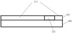
进一步的,所述显示面板包括玻璃层100、衬底层101和其他功能层,如图3所示,其仅图示了其中的玻璃层100和衬底层101。其中所述衬底层101包括位置对应于所述第一显示区域11的第一部111和位置对应于所述第二显示区域12的第二部121。Further, the display panel includes a
其中所述第一部111采用第一PI材料构成,其可以是业界常用的淡黄色PI材料,其中其对于可见光的蓝紫光段的透过率大致为30%。而所述第二部121采用第二PI材料构成,其为一种透明的PI材料,其对于可见光的整体透过率为80%或以上,其中对于可见光的蓝紫光段的透过率为50%或以上。The
其中所述衬底层101的第二部121采用透明的PI材料构成,可以在一定程度上有效提高其对于入射光的穿透率,从而使得对应设置在其下方感光器件,例如,摄像头,或是其他影像传感器,可以获得足够的光线,以保证其能正常的实施拍摄功能。The
而在其他实施方式中,其中所述衬底层101的第一部111也可以是采用所述第二PI材料构成,但不限于。In other embodiments, the
进一步的,请参阅图4所示,其中所述衬底层101下设置的其他功能层包括器件阵列层102、有机发光(EL)层103、封装(TFE)层104、触控(DOT)层105以及模组(MOD)器件层106。Further, please refer to FIG. 4 , wherein other functional layers disposed under the
其中所述器件阵列层102中设置有像素阵列,其中所述像素阵列包括对应设置在所述第一显示区域11的第一像素阵列和对应设置在所述第二显示区域的第二像素阵列,其中在相同单位面积下所述第一像素阵列的像素阵列密度大于所述第二像素阵列的像素阵列密度。其中所述单位面积可以是厘米单位级,也可以是毫米单位级,具体可随需要而定,并无限定。The
其中所述第一像素阵列的像素阵列密度是第二像素阵列的像素阵列密度的1~10倍。例如,在一个实施方式中,其中在同样单位面积下所述第一像素阵列为10X10的像素阵列,而所述第二像素阵列为4X4的像素阵列。The pixel array density of the first pixel array is 1-10 times that of the second pixel array. For example, in one embodiment, under the same unit area, the first pixel array is a 10×10 pixel array, and the second pixel array is a 4×4 pixel array.
具体来讲,设每个像素尺寸为63um*63um,所述第一像素阵列在单位平方毫米内设置的像素数量为252个,而所述第二像素阵列在同样的单位平方毫米内设置的像素阵列密度可以为所述第一像素阵列的阵列密度的1/4、1/9、1/16、1/25、1/36等等,具体可随实际需要而定,并无限定。Specifically, assuming that the size of each pixel is 63um*63um, the number of pixels set in the first pixel array in a unit square millimeter is 252, and the pixels set in the second pixel array in the same unit square millimeter The array density may be 1/4, 1/9, 1/16, 1/25, 1/36, etc. of the array density of the first pixel array, which may be determined according to actual needs and is not limited.
本发明将位置对应于所述第二显示区域12的像素阵列密度降低,采用稀疏的阵列排布,如此,可在保留所述第二显示区域12显示功能的同时,还能起到不影响透光的作用,进而不会因保留显示功能而影响其下方设置的感光器件的正常功能实施。In the present invention, the pixel array density corresponding to the
进一步的,其中所述第二显示区域12中的相邻像素之间的区域设置有透光通道。其中降低所述第二显示区域12内的像素阵列密度的目的,即为增加像素之间的空间,以便使得更多的光能从像素之间的区域入射到其下方的影像传感单元中,因此,所述第二显示区域12内相邻像素之间的区域要能尽量透光,进而可将两像素之间的区域定义为所述透光通道。进一步的,对于所述透光通道内的各膜层结构所采用的材料而言,其也尽量选用透光率高的材料构成。例如,例如,该区域内不适合设置由具有高光密度系数材料构成的像素定义层。Further, the area between adjacent pixels in the
进一步的,其中所述单元阵列层102中包括像素定义层1022,其中所述像素定义层1022采用的光阻材料能够遮住其所在单元阵列层102中的金属走线层对入射光的衍射以及反光。例如,所述像素定义层1022采用的是一种黑色光阻材料,其光密度OD(OpticalDensity;OD=-lgT,其中T为穿透率;)值大于0.2,优选值在0.3或以上。Further, the
这一光阻材料的变更,从技术效果方面来讲,以所述第二显示区域为例而言,其可以有效改善其位置处的所述器件阵列层102中的金属膜层衍射以及反光的现象,同时还可以改善发光区域不同像素之间的漏光现象。更为重要的是,若是所述显示面板的整体显示区域的像素定义层均采用本发明涉及的所述光阻材料,其可以去除后续的POL这道制程,在一定程度上简化了所述显示面板的制程工艺。In terms of technical effect, the change of the photoresist material, taking the second display area as an example, can effectively improve the diffraction and reflection of the metal film layer in the
进一步的,本发明的又一实施方式提供了一种终端器件,其包括本体,其中所述本体上设置有感光器件,例如,摄像头。所述本体上还设置有本发明涉及的所述显示面板,其中所述感光器件对应设置在所述显示面板的第二显示区域下。Further, another embodiment of the present invention provides a terminal device, which includes a body, wherein a photosensitive device, such as a camera, is disposed on the body. The display panel according to the present invention is also disposed on the body, wherein the photosensitive device is correspondingly disposed under the second display area of the display panel.
其中所述终端器件可以是任何需要设置显示面板以及在所述显示面板下设置感光器件的智能终端器件。例如,手机、平板、电脑等等。The terminal device may be any intelligent terminal device that needs to be provided with a display panel and a photosensitive device under the display panel. For example, mobile phones, tablets, computers, etc.
本发明涉及的一种显示面板,其在其衬底层特定区域,例如,摄像头区域,采用本发明涉及的透明PI材料构成,使得该区域的透光性获得了极大改善,从而使得其下方设置的摄像头能够获得足够的光线进行正常的拍摄操作;同时降低该区域内的器件阵列层中的像素阵列密度,使得该区域仍具有显示功能,如此,则使得本发明涉及的所述显示面板,具有整体上的有效显示区域,而不存在为保持下方摄像头正常的拍摄功能而妥协设置的一处非显示区域,从而在一定程度上实现了市场上高度需求的“全面屏”的显示效果。这一“全面屏”的显示效果,明显会提升其所在终端器件使用顾客的满意度,因此,可以认为本发明涉及的所述显示面板是面板行业的发展趋势。The present invention relates to a display panel, which is made of the transparent PI material involved in the present invention in a specific area of its substrate layer, for example, the camera area, so that the light transmittance of this area is greatly improved, so that the lower part of the display panel is The camera can obtain enough light for normal shooting operations; at the same time, the pixel array density in the device array layer in this area is reduced, so that this area still has a display function, so that the display panel involved in the present invention has The overall effective display area does not have a non-display area that is compromised to maintain the normal shooting function of the camera below, thus achieving the "full screen" display effect that is highly demanded in the market to a certain extent. The display effect of this "full screen" will obviously improve the satisfaction of customers who use the terminal device where it is located. Therefore, it can be considered that the display panel involved in the present invention is the development trend of the panel industry.
进一步的,在摄像头区域的所述单元阵列层中的像素定义层采用本发明涉及的新型功能材料黑色有机光阻取代传统有机光阻,由于黑色光阻材料其对于光线的吸收性能,使得其能够起到一定的遮挡作用,从而有效改善该区域摄像头位置处所述器件阵列层中的金属走线对入射光线的衍射以及反光的现象,同时还能改善其发光区域中不同像素之间的漏光现象。Further, the pixel definition layer in the unit array layer in the camera area adopts the new functional material black organic photoresist involved in the present invention to replace the traditional organic photoresist. Play a certain shading effect, so as to effectively improve the diffraction and reflection of incident light by the metal traces in the device array layer at the location of the camera in this area, and also improve the phenomenon of light leakage between different pixels in the light-emitting area. .
更为重要的是,由于引入的所述黑色光阻材料的遮光效能,若是所述显示面板的整体显示区域的像素定义层均采用本发明涉及的所述光阻材料,使得本发明涉及的所述显示面板的制程不再需要后续的POL这道制程。如此,精简了本发明涉及的显示面板的制程工艺,More importantly, due to the shading effect of the black photoresist material introduced, if the photoresist material involved in the present invention is used in the pixel definition layer of the entire display area of the display panel, the The process of the display panel described above does not require the subsequent POL process. In this way, the manufacturing process of the display panel involved in the present invention is simplified,
另外,本发明涉及的所述显示面板,也不在需要采用镭射切割的方式通过现有技术中常见的异形屏来实现屏下摄像头的正常拍摄操作,从而避免了显示屏在镭射过程中微粒增加以及断裂风险,同时又不会增加设备成本,更有助于将来的量产化。In addition, the display panel involved in the present invention no longer needs to use the laser cutting method to realize the normal shooting operation of the under-screen camera through the special-shaped screen common in the prior art, thereby avoiding the increase of particles on the display screen during the laser process. The risk of fracture will not increase the cost of equipment at the same time, which is more conducive to future mass production.
本发明的技术范围不仅仅局限于上述说明中的内容,本领域技术人员可以在不脱离本发明技术思想的前提下,对上述实施例进行多种变形和修改,而这些变形和修改均应当属于本发明的范围内。The technical scope of the present invention is not limited to the content in the above description, and those skilled in the art can make various deformations and modifications to the above-mentioned embodiments without departing from the technical idea of the present invention, and these deformations and modifications should belong to within the scope of the present invention.
Claims (9)
Priority Applications (3)
| Application Number | Priority Date | Filing Date | Title |
|---|---|---|---|
| CN201811635335.5ACN111384064B (en) | 2018-12-29 | 2018-12-29 | Display panel and terminal device thereof |
| US16/476,282US20210335919A1 (en) | 2018-12-29 | 2019-04-08 | Display panel and terminal device thereof |
| PCT/CN2019/081745WO2020133789A1 (en) | 2018-12-29 | 2019-04-08 | Display panel and terminal device thereof |
Applications Claiming Priority (1)
| Application Number | Priority Date | Filing Date | Title |
|---|---|---|---|
| CN201811635335.5ACN111384064B (en) | 2018-12-29 | 2018-12-29 | Display panel and terminal device thereof |
Publications (2)
| Publication Number | Publication Date |
|---|---|
| CN111384064A CN111384064A (en) | 2020-07-07 |
| CN111384064Btrue CN111384064B (en) | 2022-05-31 |
Family
ID=71126717
Family Applications (1)
| Application Number | Title | Priority Date | Filing Date |
|---|---|---|---|
| CN201811635335.5AActiveCN111384064B (en) | 2018-12-29 | 2018-12-29 | Display panel and terminal device thereof |
Country Status (3)
| Country | Link |
|---|---|
| US (1) | US20210335919A1 (en) |
| CN (1) | CN111384064B (en) |
| WO (1) | WO2020133789A1 (en) |
Families Citing this family (4)
| Publication number | Priority date | Publication date | Assignee | Title |
|---|---|---|---|---|
| CN110288943B (en)* | 2019-07-08 | 2020-10-16 | 武汉华星光电半导体显示技术有限公司 | Display panel and display device |
| KR20210044946A (en)* | 2019-10-15 | 2021-04-26 | 삼성디스플레이 주식회사 | Apparatus and method for manufacturing a display apparatus |
| CN110752233B (en)* | 2019-10-25 | 2022-07-05 | 武汉天马微电子有限公司 | Flexible display panel, manufacturing method thereof and flexible display device |
| CN112259575B (en)* | 2020-09-24 | 2024-05-31 | 维信诺科技股份有限公司 | Display panel and electronic terminal |
Family Cites Families (10)
| Publication number | Priority date | Publication date | Assignee | Title |
|---|---|---|---|---|
| CN204271085U (en)* | 2014-12-05 | 2015-04-15 | 昆山工研院新型平板显示技术中心有限公司 | An organic light emitting display device |
| KR102292227B1 (en)* | 2015-03-02 | 2021-08-24 | 삼성디스플레이 주식회사 | Transparent display devices and methods of manufacturing the same |
| CN105810714B (en)* | 2016-03-16 | 2019-03-15 | 武汉华星光电技术有限公司 | OLED display device with double-sided display and manufacturing method thereof |
| KR102670056B1 (en)* | 2016-11-18 | 2024-05-30 | 삼성디스플레이 주식회사 | Display apparatus and method of manufacturing the same |
| KR102373308B1 (en)* | 2017-04-06 | 2022-03-11 | 삼성전자주식회사 | Electronic device including a housing having at least one through hole |
| CN107946341B (en)* | 2017-11-10 | 2020-05-22 | 上海天马微电子有限公司 | Display device and method for manufacturing display device |
| CN208200811U (en)* | 2018-03-14 | 2018-12-07 | 武汉依麦德新材料科技有限责任公司 | A kind of polyimides fenestrated membrane |
| CN208271897U (en)* | 2018-03-16 | 2018-12-21 | 华为技术有限公司 | A kind of display screen and display terminal |
| CN108615822A (en)* | 2018-04-28 | 2018-10-02 | 武汉华星光电半导体显示技术有限公司 | Flexible OLED display panel and preparation method thereof, display device |
| CN208257874U (en)* | 2018-06-07 | 2018-12-18 | 信利光电股份有限公司 | A kind of comprehensive screen mobile phone |
- 2018
- 2018-12-29CNCN201811635335.5Apatent/CN111384064B/enactiveActive
- 2019
- 2019-04-08USUS16/476,282patent/US20210335919A1/ennot_activeAbandoned
- 2019-04-08WOPCT/CN2019/081745patent/WO2020133789A1/ennot_activeCeased
Also Published As
| Publication number | Publication date |
|---|---|
| WO2020133789A1 (en) | 2020-07-02 |
| CN111384064A (en) | 2020-07-07 |
| US20210335919A1 (en) | 2021-10-28 |
Similar Documents
| Publication | Publication Date | Title |
|---|---|---|
| CN112349759B (en) | Display panel and display device | |
| US10620768B2 (en) | Flexible display panel, manufacturing method thereof and display device | |
| CN111384064B (en) | Display panel and terminal device thereof | |
| WO2021036157A1 (en) | Liquid crystal display panel, liquid crystal display apparatus and electronic device | |
| CN111081752B (en) | Display panel and display device | |
| WO2020228236A1 (en) | Display device | |
| CN107966843B (en) | display device | |
| CN112928148A (en) | Display panel and electronic device | |
| CN113156732B (en) | Reflective display panel and manufacturing method thereof, and display device | |
| CN104536179A (en) | Flat panel display | |
| CN110967857A (en) | Liquid crystal display panel | |
| WO2022206832A1 (en) | Display panel and electronic device | |
| CN115236894B (en) | Display panel, manufacturing method thereof and display device | |
| CN107037648A (en) | A kind of array base palte and preparation method thereof, display panel, display device | |
| CN103995390B (en) | The manufacture method of display floater, display device and display floater | |
| CN113630486B (en) | Electronic equipment and displays | |
| CN111208675B (en) | Display panels and display devices | |
| WO2021213022A1 (en) | Display module, display assembly, and electronic device | |
| KR101969319B1 (en) | Display device having transparent bezel border | |
| WO2023109239A1 (en) | Display panel and display device | |
| JP2010224081A (en) | Display device | |
| CN108108045A (en) | Touch base plate, touch screen and its manufacturing method, display device | |
| CN206021808U (en) | A kind of flexible display panels and display device | |
| CN104820257A (en) | Light guide plate, backlight source and display device | |
| WO2019037286A1 (en) | Transflective liquid crystal display device |
Legal Events
| Date | Code | Title | Description |
|---|---|---|---|
| PB01 | Publication | ||
| PB01 | Publication | ||
| SE01 | Entry into force of request for substantive examination | ||
| SE01 | Entry into force of request for substantive examination | ||
| GR01 | Patent grant | ||
| GR01 | Patent grant |