CN111383995A - Method for manufacturing semiconductor device - Google Patents
Method for manufacturing semiconductor deviceDownload PDFInfo
- Publication number
- CN111383995A CN111383995ACN201911285736.7ACN201911285736ACN111383995ACN 111383995 ACN111383995 ACN 111383995ACN 201911285736 ACN201911285736 ACN 201911285736ACN 111383995 ACN111383995 ACN 111383995A
- Authority
- CN
- China
- Prior art keywords
- region
- insulating film
- gate electrode
- gate
- semiconductor
- Prior art date
- Legal status (The legal status is an assumption and is not a legal conclusion. Google has not performed a legal analysis and makes no representation as to the accuracy of the status listed.)
- Granted
Links
Images


Classifications
- H—ELECTRICITY
- H10—SEMICONDUCTOR DEVICES; ELECTRIC SOLID-STATE DEVICES NOT OTHERWISE PROVIDED FOR
- H10D—INORGANIC ELECTRIC SEMICONDUCTOR DEVICES
- H10D64/00—Electrodes of devices having potential barriers
- H10D64/01—Manufacture or treatment
- H10D64/017—Manufacture or treatment using dummy gates in processes wherein at least parts of the final gates are self-aligned to the dummy gates, i.e. replacement gate processes
- H—ELECTRICITY
- H10—SEMICONDUCTOR DEVICES; ELECTRIC SOLID-STATE DEVICES NOT OTHERWISE PROVIDED FOR
- H10B—ELECTRONIC MEMORY DEVICES
- H10B43/00—EEPROM devices comprising charge-trapping gate insulators
- H—ELECTRICITY
- H10—SEMICONDUCTOR DEVICES; ELECTRIC SOLID-STATE DEVICES NOT OTHERWISE PROVIDED FOR
- H10B—ELECTRONIC MEMORY DEVICES
- H10B43/00—EEPROM devices comprising charge-trapping gate insulators
- H10B43/30—EEPROM devices comprising charge-trapping gate insulators characterised by the memory core region
- H10B43/35—EEPROM devices comprising charge-trapping gate insulators characterised by the memory core region with cell select transistors, e.g. NAND
- H—ELECTRICITY
- H10—SEMICONDUCTOR DEVICES; ELECTRIC SOLID-STATE DEVICES NOT OTHERWISE PROVIDED FOR
- H10B—ELECTRONIC MEMORY DEVICES
- H10B43/00—EEPROM devices comprising charge-trapping gate insulators
- H10B43/40—EEPROM devices comprising charge-trapping gate insulators characterised by the peripheral circuit region
- H—ELECTRICITY
- H10—SEMICONDUCTOR DEVICES; ELECTRIC SOLID-STATE DEVICES NOT OTHERWISE PROVIDED FOR
- H10D—INORGANIC ELECTRIC SEMICONDUCTOR DEVICES
- H10D30/00—Field-effect transistors [FET]
- H10D30/01—Manufacture or treatment
- H10D30/021—Manufacture or treatment of FETs having insulated gates [IGFET]
- H10D30/0223—Manufacture or treatment of FETs having insulated gates [IGFET] having source and drain regions or source and drain extensions self-aligned to sides of the gate
- H10D30/0227—Manufacture or treatment of FETs having insulated gates [IGFET] having source and drain regions or source and drain extensions self-aligned to sides of the gate having both lightly-doped source and drain extensions and source and drain regions self-aligned to the sides of the gate, e.g. lightly-doped drain [LDD] MOSFET or double-diffused drain [DDD] MOSFET
- H—ELECTRICITY
- H10—SEMICONDUCTOR DEVICES; ELECTRIC SOLID-STATE DEVICES NOT OTHERWISE PROVIDED FOR
- H10D—INORGANIC ELECTRIC SEMICONDUCTOR DEVICES
- H10D64/00—Electrodes of devices having potential barriers
- H10D64/01—Manufacture or treatment
- H10D64/021—Manufacture or treatment using multiple gate spacer layers, e.g. bilayered sidewall spacers
- H—ELECTRICITY
- H10—SEMICONDUCTOR DEVICES; ELECTRIC SOLID-STATE DEVICES NOT OTHERWISE PROVIDED FOR
- H10D—INORGANIC ELECTRIC SEMICONDUCTOR DEVICES
- H10D64/00—Electrodes of devices having potential barriers
- H10D64/60—Electrodes characterised by their materials
- H10D64/66—Electrodes having a conductor capacitively coupled to a semiconductor by an insulator, e.g. MIS electrodes
- H10D64/68—Electrodes having a conductor capacitively coupled to a semiconductor by an insulator, e.g. MIS electrodes characterised by the insulator, e.g. by the gate insulator
- H10D64/681—Electrodes having a conductor capacitively coupled to a semiconductor by an insulator, e.g. MIS electrodes characterised by the insulator, e.g. by the gate insulator having a compositional variation, e.g. multilayered
- H10D64/685—Electrodes having a conductor capacitively coupled to a semiconductor by an insulator, e.g. MIS electrodes characterised by the insulator, e.g. by the gate insulator having a compositional variation, e.g. multilayered being perpendicular to the channel plane
- H—ELECTRICITY
- H10—SEMICONDUCTOR DEVICES; ELECTRIC SOLID-STATE DEVICES NOT OTHERWISE PROVIDED FOR
- H10D—INORGANIC ELECTRIC SEMICONDUCTOR DEVICES
- H10D84/00—Integrated devices formed in or on semiconductor substrates that comprise only semiconducting layers, e.g. on Si wafers or on GaAs-on-Si wafers
- H10D84/01—Manufacture or treatment
- H10D84/0123—Integrating together multiple components covered by H10D12/00 or H10D30/00, e.g. integrating multiple IGBTs
- H10D84/0126—Integrating together multiple components covered by H10D12/00 or H10D30/00, e.g. integrating multiple IGBTs the components including insulated gates, e.g. IGFETs
- H10D84/0128—Manufacturing their channels
- H—ELECTRICITY
- H10—SEMICONDUCTOR DEVICES; ELECTRIC SOLID-STATE DEVICES NOT OTHERWISE PROVIDED FOR
- H10D—INORGANIC ELECTRIC SEMICONDUCTOR DEVICES
- H10D84/00—Integrated devices formed in or on semiconductor substrates that comprise only semiconducting layers, e.g. on Si wafers or on GaAs-on-Si wafers
- H10D84/01—Manufacture or treatment
- H10D84/0123—Integrating together multiple components covered by H10D12/00 or H10D30/00, e.g. integrating multiple IGBTs
- H10D84/0126—Integrating together multiple components covered by H10D12/00 or H10D30/00, e.g. integrating multiple IGBTs the components including insulated gates, e.g. IGFETs
- H10D84/0135—Manufacturing their gate conductors
- H—ELECTRICITY
- H10—SEMICONDUCTOR DEVICES; ELECTRIC SOLID-STATE DEVICES NOT OTHERWISE PROVIDED FOR
- H10D—INORGANIC ELECTRIC SEMICONDUCTOR DEVICES
- H10D84/00—Integrated devices formed in or on semiconductor substrates that comprise only semiconducting layers, e.g. on Si wafers or on GaAs-on-Si wafers
- H10D84/01—Manufacture or treatment
- H10D84/0123—Integrating together multiple components covered by H10D12/00 or H10D30/00, e.g. integrating multiple IGBTs
- H10D84/0126—Integrating together multiple components covered by H10D12/00 or H10D30/00, e.g. integrating multiple IGBTs the components including insulated gates, e.g. IGFETs
- H10D84/0144—Manufacturing their gate insulating layers
- H—ELECTRICITY
- H10—SEMICONDUCTOR DEVICES; ELECTRIC SOLID-STATE DEVICES NOT OTHERWISE PROVIDED FOR
- H10D—INORGANIC ELECTRIC SEMICONDUCTOR DEVICES
- H10D84/00—Integrated devices formed in or on semiconductor substrates that comprise only semiconducting layers, e.g. on Si wafers or on GaAs-on-Si wafers
- H10D84/01—Manufacture or treatment
- H10D84/0123—Integrating together multiple components covered by H10D12/00 or H10D30/00, e.g. integrating multiple IGBTs
- H10D84/0126—Integrating together multiple components covered by H10D12/00 or H10D30/00, e.g. integrating multiple IGBTs the components including insulated gates, e.g. IGFETs
- H10D84/0147—Manufacturing their gate sidewall spacers
- H—ELECTRICITY
- H10—SEMICONDUCTOR DEVICES; ELECTRIC SOLID-STATE DEVICES NOT OTHERWISE PROVIDED FOR
- H10D—INORGANIC ELECTRIC SEMICONDUCTOR DEVICES
- H10D84/00—Integrated devices formed in or on semiconductor substrates that comprise only semiconducting layers, e.g. on Si wafers or on GaAs-on-Si wafers
- H10D84/01—Manufacture or treatment
- H10D84/02—Manufacture or treatment characterised by using material-based technologies
- H10D84/03—Manufacture or treatment characterised by using material-based technologies using Group IV technology, e.g. silicon technology or silicon-carbide [SiC] technology
- H10D84/038—Manufacture or treatment characterised by using material-based technologies using Group IV technology, e.g. silicon technology or silicon-carbide [SiC] technology using silicon technology, e.g. SiGe
- H—ELECTRICITY
- H10—SEMICONDUCTOR DEVICES; ELECTRIC SOLID-STATE DEVICES NOT OTHERWISE PROVIDED FOR
- H10D—INORGANIC ELECTRIC SEMICONDUCTOR DEVICES
- H10D84/00—Integrated devices formed in or on semiconductor substrates that comprise only semiconducting layers, e.g. on Si wafers or on GaAs-on-Si wafers
- H10D84/80—Integrated devices formed in or on semiconductor substrates that comprise only semiconducting layers, e.g. on Si wafers or on GaAs-on-Si wafers characterised by the integration of at least one component covered by groups H10D12/00 or H10D30/00, e.g. integration of IGFETs
- H10D84/82—Integrated devices formed in or on semiconductor substrates that comprise only semiconducting layers, e.g. on Si wafers or on GaAs-on-Si wafers characterised by the integration of at least one component covered by groups H10D12/00 or H10D30/00, e.g. integration of IGFETs of only field-effect components
- H10D84/83—Integrated devices formed in or on semiconductor substrates that comprise only semiconducting layers, e.g. on Si wafers or on GaAs-on-Si wafers characterised by the integration of at least one component covered by groups H10D12/00 or H10D30/00, e.g. integration of IGFETs of only field-effect components of only insulated-gate FETs [IGFET]
- H10D84/8314—Integrated devices formed in or on semiconductor substrates that comprise only semiconducting layers, e.g. on Si wafers or on GaAs-on-Si wafers characterised by the integration of at least one component covered by groups H10D12/00 or H10D30/00, e.g. integration of IGFETs of only field-effect components of only insulated-gate FETs [IGFET] the IGFETs characterised by having gate insulating layers with different properties
- H—ELECTRICITY
- H10—SEMICONDUCTOR DEVICES; ELECTRIC SOLID-STATE DEVICES NOT OTHERWISE PROVIDED FOR
- H10D—INORGANIC ELECTRIC SEMICONDUCTOR DEVICES
- H10D86/00—Integrated devices formed in or on insulating or conducting substrates, e.g. formed in silicon-on-insulator [SOI] substrates or on stainless steel or glass substrates
- H10D86/01—Manufacture or treatment
- H—ELECTRICITY
- H10—SEMICONDUCTOR DEVICES; ELECTRIC SOLID-STATE DEVICES NOT OTHERWISE PROVIDED FOR
- H10D—INORGANIC ELECTRIC SEMICONDUCTOR DEVICES
- H10D86/00—Integrated devices formed in or on insulating or conducting substrates, e.g. formed in silicon-on-insulator [SOI] substrates or on stainless steel or glass substrates
- H10D86/201—Integrated devices formed in or on insulating or conducting substrates, e.g. formed in silicon-on-insulator [SOI] substrates or on stainless steel or glass substrates the substrates comprising an insulating layer on a semiconductor body, e.g. SOI
- H—ELECTRICITY
- H10—SEMICONDUCTOR DEVICES; ELECTRIC SOLID-STATE DEVICES NOT OTHERWISE PROVIDED FOR
- H10D—INORGANIC ELECTRIC SEMICONDUCTOR DEVICES
- H10D87/00—Integrated devices comprising both bulk components and either SOI or SOS components on the same substrate
Landscapes
- Thin Film Transistor (AREA)
- Metal-Oxide And Bipolar Metal-Oxide Semiconductor Integrated Circuits (AREA)
- Semiconductor Memories (AREA)
- Non-Volatile Memory (AREA)
- Insulated Gate Type Field-Effect Transistor (AREA)
Abstract
Translated fromChinese
Description
Translated fromChinese相关申请的交叉引用CROSS-REFERENCE TO RELATED APPLICATIONS
于2018年12月26日提交的日本专利申请No.2018-243513的公开(包括说明书、附图和摘要)通过引用整体合并于此。The disclosure of Japanese Patent Application No. 2018-243513 filed on December 26, 2018, including the specification, drawings and abstract, is hereby incorporated by reference in its entirety.
背景技术Background technique
本发明涉及半导体器件的制造方法,例如,本发明涉及可以应用于使用SOI衬底的半导体器件的技术。The present invention relates to a method of manufacturing a semiconductor device, for example, the present invention relates to a technique that can be applied to a semiconductor device using an SOI substrate.
专利文献1(JP特开2013-84766)公开了通过后栅极方法制造具有其中混合有SOI结构(SOI型MISFET形成区域Rs)和体结构(体型MISFET形成区域Rb)的所谓的混合衬底结构的半导体集成电路装置。具体地,文献1描述了一种与包括金属栅电极的SOI(绝缘体上硅)型MISFET(金属绝缘体半导体场效应晶体管)和多晶硅栅电极的体型MISFET的半导体集成电路装置相关的技术。Patent Document 1 (JP Laid-Open No. 2013-84766 ) discloses the manufacture of a so-called hybrid substrate structure having an SOI structure (SOI type MISFET formation region Rs) and a bulk structure (body type MISFET formation region Rb) mixed therein by a gate last method semiconductor integrated circuit device. Specifically,
专利文献2(JP特开2018-26457)公开了一种具有形成有非易失性存储器的存储元件(存储元件、存储单元)MC的存储区域1A、形成有低击穿电压MISFET2的低击穿电压MISFET形成区域1B、和形成高击穿电压MISFET3的高击穿电压MISFET形成区域1C的半导体器件、以及与其制造方法相关的技术。Patent Document 2 (JP Laid-Open No. 2018-26457) discloses a
发明内容SUMMARY OF THE INVENTION
本发明人研究了在例如专利文献1、例如专利文献2所示的体型MISFET形成区域(下文中称为“体区”)中混合多种类型的MISFET。本发明人已经研究了不仅对于形成在SOI型MISFET形成区域(下文中称为“SOI区域”)中的MISFET的栅电极,而且对于形成在上述体区中的相应MISFET的栅电极采用金属栅电极结构。根据本发明人的研究,已经发现,如果将上述文献1中所示的后栅极方法简单地用于上述结构(结构),则不能将相应MISFET的栅电极形成为期望的形状,结果,半导体器件的可靠性(即,电特性)可能降低。The present inventors have studied mixing various types of MISFETs in a body-type MISFET formation region (hereinafter referred to as a “body region”) shown in, for example,
从本说明书的描述和附图,其他目的和新颖特征将变得很清楚。Other objects and novel features will become apparent from the description of the present specification and the accompanying drawings.
下面将简要描述本申请中公开的典型实施例。Exemplary embodiments disclosed in this application will be briefly described below.
在一个实施例中的制造半导体器件的方法中,首先,在位于衬底的体区中的半导体层和位于体区中的绝缘层被去除之后,在位于体区的第一区域中的半导体基底材料的表面上执行外延生长处理。并且,分别地,经由第一栅极绝缘膜在位于衬底的SOI区域中的半导体层上形成第一栅电极,经由第二栅极绝缘膜在位于体区的第一区域中并且被执行外延生长处理的半导体基底材料上形成第二栅电极,并且经由第三栅极绝缘膜在位于体区的第二区域中并且未被执行外延生长处理的半导体基底材料上形成第三栅电极。在此,第三栅极绝缘膜的厚度大于第一栅极绝缘膜和第二栅极绝缘膜中的每个栅极绝缘膜的厚度。并且,第一栅电极至第三栅电极中的每个栅电极由第一材料制成。之后,形成在衬底上以覆盖第一栅电极至第三栅电极中的每个栅电极的层间绝缘膜被抛光。并且,在将第一栅电极至第三栅电极中的每个栅电极从层间绝缘膜暴露之后,组成第一栅电极至第三栅电极中的每个栅电极的第一材料被替换为不同于第一材料的第二材料。In a method of manufacturing a semiconductor device in one embodiment, first, after the semiconductor layer located in the body region of the substrate and the insulating layer located in the body region are removed, the semiconductor substrate located in the first region of the body region An epitaxial growth process is performed on the surface of the material. And, respectively, a first gate electrode is formed on the semiconductor layer located in the SOI region of the substrate via the first gate insulating film, and epitaxy is performed in the first region located in the body region via the second gate insulating film A second gate electrode is formed on the growth-processed semiconductor base material, and a third gate electrode is formed on the semiconductor base material located in the second region of the body region and not subjected to the epitaxial growth process via a third gate insulating film. Here, the thickness of the third gate insulating film is greater than the thickness of each of the first gate insulating film and the second gate insulating film. And, each of the first to third gate electrodes is made of the first material. After that, an interlayer insulating film formed on the substrate to cover each of the first to third gate electrodes is polished. And, after exposing each of the first to third gate electrodes from the interlayer insulating film, the first material constituting each of the first to third gate electrodes is replaced with A second material different from the first material.
在一个实施例中的制造半导体器件的方法中,首先,在位于衬底的体区中的半导体层和位于体区中的绝缘层被去除之后,在位于体区的第一区域中的半导体基底材料的表面上执行外延生长处理,从而形成外延生长层。并且,分别地,经由第一栅极绝缘膜在位于衬底的SOI区域中的半导体层上形成第一栅电极,经由第二栅极绝缘膜在位于体区的第一区域中的外延生长层上形成第二栅电极,并且经由第三栅极绝缘膜在位于体区的第二区域中并且未被执行外延生长处理的半导体基底材料上形成第三栅电极。在此,第三栅极绝缘膜具有由氧化硅组成的第一绝缘层、形成在第一绝缘层上的由氮化硅组成的第二绝缘层、以及形成在第二绝缘层上的由氧化硅组成的第三绝缘层。并且,第三栅极绝缘膜的厚度大于第一栅极绝缘膜和第二栅极绝缘膜中的每个栅极绝缘膜的厚度。此外,第一栅电极至第三栅电极中的每个栅电极由多晶硅制成。之后,形成在衬底上以覆盖第一栅电极至第三栅电极中的每个栅电极的层间绝缘膜被抛光。并且,在将第一栅电极至第三栅电极中的每个栅电极从层间绝缘膜暴露之后,通过去除第一栅电极至第三栅电极中的每个栅电极而形成的间隙被填充以金属膜。In a method of manufacturing a semiconductor device in one embodiment, first, after the semiconductor layer located in the body region of the substrate and the insulating layer located in the body region are removed, the semiconductor substrate located in the first region of the body region An epitaxial growth process is performed on the surface of the material, thereby forming an epitaxial growth layer. And, respectively, a first gate electrode is formed on the semiconductor layer located in the SOI region of the substrate via the first gate insulating film, and an epitaxially grown layer located in the first region of the body region via the second gate insulating film A second gate electrode is formed thereon, and a third gate electrode is formed on the semiconductor base material located in the second region of the body region and not subjected to an epitaxial growth process via a third gate insulating film. Here, the third gate insulating film has a first insulating layer made of silicon oxide, a second insulating layer made of silicon nitride formed on the first insulating layer, and a second insulating layer made of oxide formed on the second insulating layer A third insulating layer composed of silicon. Also, the thickness of the third gate insulating film is greater than the thickness of each of the first gate insulating film and the second gate insulating film. In addition, each of the first to third gate electrodes is made of polysilicon. After that, an interlayer insulating film formed on the substrate to cover each of the first to third gate electrodes is polished. And, after exposing each of the first to third gate electrodes from the interlayer insulating film, a gap formed by removing each of the first to third gate electrodes is filled with metal film.
此外,在一个实施例中的制造半导体器件的方法中,首先,在位于衬底的体区中的半导体层和位于体区中的绝缘层被去除之后,通过在位于体区的第一区域中的半导体基底材料的表面和位于体区的第二区域的第二部分中的半导体基底材料的表面中的每个表面上执行外延生长处理来形成外延生长层。并且,经由第一栅极绝缘膜在位于SOI区域中的半导体层上形成第一栅电极,经由第二栅极绝缘膜在位于体区的第一区域中的外延生长层上形成第二栅电极,经由第三栅极绝缘膜在位于体区的第二区域的第一部分中的半导体基底材料上形成第三栅电极,并且经由第四绝缘膜在位于体区的第二区域的第二部分中的外延生长层上形成第四栅电极。在此,第三栅极绝缘膜具有由氧化硅组成的第一绝缘层、形成在第一绝缘层上的由氮化硅组成的第二绝缘层、以及形成在第二绝缘层上的由氧化硅组成的第三绝缘层。并且,第三栅极绝缘膜的厚度大于第一栅极绝缘膜、第二栅极绝缘膜和第四栅极绝缘膜中的每个栅极绝缘膜的厚度。此外,第一栅电极至第四栅电极中的每个栅电极由第一材料制成。之后,形成在衬底上以覆盖第一栅电极至第四栅电极中的每个栅电极的层间绝缘膜被抛光。并且,在将第一栅电极至第四栅电极中的每个栅电极从层间绝缘膜暴露之后,将组成第一栅电极至第四栅电极中的每个栅电极的第一材料替换为不同于第一材料的第二材料。Furthermore, in the method of manufacturing a semiconductor device in one embodiment, first, after the semiconductor layer located in the body region of the substrate and the insulating layer located in the body region are removed, the first region located in the body region is An epitaxial growth process is performed on each of the surface of the semiconductor base material and the surface of the semiconductor base material located in the second portion of the second region of the body region to form an epitaxial growth layer. And, a first gate electrode is formed on the semiconductor layer located in the SOI region via a first gate insulating film, and a second gate electrode is formed on the epitaxial growth layer located in the first region of the body region via a second gate insulating film , a third gate electrode is formed on the semiconductor base material in the first portion of the second region of the body region via the third gate insulating film, and in the second portion of the second region of the body region via the fourth insulating film A fourth gate electrode is formed on the epitaxial growth layer. Here, the third gate insulating film has a first insulating layer made of silicon oxide, a second insulating layer made of silicon nitride formed on the first insulating layer, and a second insulating layer made of oxide formed on the second insulating layer A third insulating layer composed of silicon. Also, the thickness of the third gate insulating film is greater than the thickness of each of the first gate insulating film, the second gate insulating film, and the fourth gate insulating film. In addition, each of the first to fourth gate electrodes is made of the first material. After that, an interlayer insulating film formed on the substrate to cover each of the first to fourth gate electrodes is polished. And, after exposing each of the first to fourth gate electrodes from the interlayer insulating film, the first material constituting each of the first to fourth gate electrodes is replaced with A second material different from the first material.
根据一个实施例,可以抑制半导体器件的可靠性的劣化。According to one embodiment, the deterioration of reliability of the semiconductor device can be suppressed.
附图说明Description of drawings
图1是第一实施例的半导体器件的主要部分平面图;FIG. 1 is a plan view of a main part of a semiconductor device of a first embodiment;
图2是图1的X射线的主要部分截面图;Fig. 2 is the main part sectional view of the X-ray of Fig. 1;
图3是示出第一实施例的半导体器件的制造过程的过程流程图;3 is a process flow diagram showing a manufacturing process of the semiconductor device of the first embodiment;
图4是在制造过程期间的第一实施例的半导体器件的主要部分截面图;4 is a main part cross-sectional view of the semiconductor device of the first embodiment during a manufacturing process;
图5是接着图4的在半导体器件的制造过程期间的主要部分截面图;FIG. 5 is a main part cross-sectional view during a manufacturing process of the semiconductor device following FIG. 4;
图6是接着图5的在半导体器件的制造过程期间的主要部分截面图;FIG. 6 is a main part cross-sectional view during a manufacturing process of the semiconductor device following FIG. 5;
图7是接着图6的在半导体器件的制造过程期间的主要部分截面图;7 is a cross-sectional view of a main part during a manufacturing process of the semiconductor device following FIG. 6;
图8是接着图7的在半导体器件的制造过程期间的主要部分截面图;8 is a cross-sectional view of a main part during a manufacturing process of the semiconductor device following FIG. 7;
图9是接着图8的在半导体器件的制造过程期间的主要部分截面图;9 is a cross-sectional view of a main part during a manufacturing process of the semiconductor device following FIG. 8;
图10是接着图9的在半导体器件的制造过程期间的主要部分截面图;FIG. 10 is a main part cross-sectional view during the manufacturing process of the semiconductor device following FIG. 9;
图11是接着图10的在半导体器件的制造过程期间的主要部分截面图;11 is a cross-sectional view of a main part during a manufacturing process of the semiconductor device following FIG. 10;
图12是接着图11的在半导体器件的制造过程期间的主要部分截面图;12 is a cross-sectional view of a main part during a manufacturing process of the semiconductor device following FIG. 11;
图13是接着图12的在半导体器件的制造过程期间的主要部分截面图;13 is a cross-sectional view of a main part during a manufacturing process of the semiconductor device following FIG. 12;
图14是接着图13的在半导体器件的制造过程期间的主要部分截面图;FIG. 14 is a main part sectional view during the manufacturing process of the semiconductor device following FIG. 13;
图15是接着图14的在半导体器件的制造过程期间的主要部分截面图;15 is a cross-sectional view of a main part during a manufacturing process of the semiconductor device following FIG. 14;
图16是在检查示例1的半导体器件的制造过程期间的主要部分截面图;16 is a main part cross-sectional view during inspection of the manufacturing process of the semiconductor device of Example 1;
图17是接着图16的在检查示例1的半导体器件的制造过程期间的主要部分截面图;17 is a main part cross-sectional view during the manufacturing process of the semiconductor device of the inspection example 1 following FIG. 16;
图18是在检查示例2的半导体器件的制造过程期间的主要部分截面图;18 is a main part cross-sectional view during inspection of the manufacturing process of the semiconductor device of Example 2;
图19是在检查示例3的半导体器件的制造过程期间的主要部分截面图;19 is a main part sectional view during the manufacturing process of the semiconductor device of the inspection example 3;
图20是接着图19的在检查示例3的半导体器件的制造过程期间的主要部分截面图;20 is a main part cross-sectional view during the manufacturing process of the semiconductor device of the inspection example 3 following FIG. 19;
图21是在检查示例4的半导体器件的制造过程期间的主要部分截面图;21 is a main part cross-sectional view during inspection of the manufacturing process of the semiconductor device of Example 4;
图22是根据第一实施例的修改示例的半导体器件的主要部分截面图;22 is a main part cross-sectional view of a semiconductor device according to a modified example of the first embodiment;
图23是第二实施例的半导体器件的示意图;以及FIG. 23 is a schematic diagram of the semiconductor device of the second embodiment; and
图24是第二实施例的半导体器件的主要部分截面图。FIG. 24 is a cross-sectional view of a main part of the semiconductor device of the second embodiment.
具体实施方式Detailed ways
在以下实施例中,当为了方便而需要时,将通过分成多个部分或实施例的方式来进行描述,但是,除非特别说明,否则这些部分或实施例不是彼此独立的,并且这些部分或实施例之一与其他部分或实施例中的部分或全部的修改示例、细节、补充说明等相关。在以下实施例中,元件等的数目(包括元件的数目、数值、数量、范围等)不限于特定数目(除非特别指定或在原则上很清楚限于特定数目),而是可以不少于或等于特定数目。此外,在以下实施例中,不用说,构成要素(包括要素步骤等)不是必须的,除非特别指定或在原则上很清楚是必须的。类似地,在以下实施例中,当参考组件等的形状、位置关系等时,假定形状等基本与形状等近似或相似,除非特别指定或在原则上很明显。这同样适用于上述数值和范围。In the following embodiments, when necessary for convenience, description will be made by being divided into a plurality of parts or embodiments, but unless otherwise specified, these parts or embodiments are not independent of each other, and these parts or embodiments One of the examples is related to other parts or some or all of the modified examples, details, supplementary explanations, and the like in the other embodiments. In the following embodiments, the number of elements and the like (including the number, value, number, range, etc. of elements) is not limited to a specific number (unless specifically specified or clearly limited to a specific number in principle), but may be not less than or equal to specific number. Furthermore, in the following embodiments, it goes without saying that the constituent elements (including the element steps and the like) are not essential unless specifically specified or clearly necessary in principle. Similarly, in the following embodiments, when referring to the shapes, positional relationships, etc. of components and the like, the shapes and the like are assumed to be substantially approximate or similar to the shapes and the like unless otherwise specified or obvious in principle. The same applies to the above numerical values and ranges.
将基于附图描述实施例的细节。在用于解释实施例的所有附图中,具有相同功能的构件由相同的附图标记表示,并且省略其重复描述。在以下实施例中,除非特别必要,否则原则上将不重复相同或相似部分的描述。Details of the embodiments will be described based on the accompanying drawings. In all the drawings for explaining the embodiments, members having the same functions are denoted by the same reference numerals, and repeated descriptions thereof are omitted. In the following embodiments, descriptions of the same or similar parts will not be repeated in principle unless particularly necessary.
在实施例中使用的附图中,即使在截面图的情况下,也可以省略阴影线,以便使附图更易于查看。此外,即使在平面图的情况下,也可以使用阴影线以使图更易于查看。In the drawings used in the embodiments, even in the case of cross-sectional views, hatching may be omitted in order to make the drawings easier to see. Also, even in the case of floor plans, hatching can be used to make the diagram easier to see.
(第一实施例)(first embodiment)
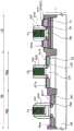
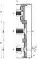
首先,将参考图1和2描述本第一实施例的半导体器件。图1是本第一实施例的半导体器件SD1的主要部分平面图。图2是图1的X射线的主要部分截面图。First, the semiconductor device of the present first embodiment will be described with reference to FIGS. 1 and 2 . FIG. 1 is a plan view of a main part of a semiconductor device SD1 of the first embodiment. FIG. 2 is a cross-sectional view of a main part of the X-ray of FIG. 1 .
(半导体器件)(Semiconductor device)
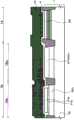
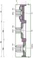
如图1和2所示,半导体器件SD1包括多个场效应晶体管(MISFET和MOSFET)Q1、Q2和Q3。在此,如图1和2所示,场效应晶体管Q1、Q2和Q3中的每个被形成在穿透半导体层SM和绝缘层BX并且被嵌入沟槽TR中以到达半导体基底材料SB的元件隔离部分ST围绕的区域(有源区域)中。As shown in FIGS. 1 and 2, the semiconductor device SD1 includes a plurality of field effect transistors (MISFETs and MOSFETs) Q1, Q2 and Q3. Here, as shown in FIGS. 1 and 2, each of the field effect transistors Q1, Q2 and Q3 is formed in an element that penetrates the semiconductor layer SM and the insulating layer BX and is embedded in the trench TR to reach the semiconductor base material SB in a region (active region) surrounded by the isolation portion ST.
如图1和2所示,半导体器件SD1包括所谓的混合结构SOI衬底(衬底)1,该衬底1包括半导体基底材料(基底材料)SB的一部分、形成在半导体基底材料SB的一部分上的绝缘层BX、具有形成在绝缘层BX上的半导体层SM的SOI(绝缘体上硅)区域1A、以及不具有绝缘层BX和半导体层SM的体区1B。为了方便起见,图1中用符号BDL表示的虚线在平面图中表示SOI区域1A与体区1B之间的边界。在图2中,该虚线基本对应于被形成为跨越SOI区域1A与体区1B之间的边界的器件隔离部分ST的阶梯表面。此外,如图2所示,体区1B具有其中通过对半导体基底材料SB的一部分执行外延生长处理而在半导体基底材料SB的表面的一部分上形成有外延生长层EP1的区域(第一区域1Ba)、以及其中在半导体基底材料SB的表面上未执行外延生长处理的区域(第二区域1Bb)。外延生长层EP1由与基底材料SB相同的材料制成。As shown in FIGS. 1 and 2 , the semiconductor device SD1 includes a so-called hybrid structure SOI substrate (substrate) 1 including a part of a semiconductor base material (base material) SB, formed on a part of the semiconductor base material SB The insulating layer BX, the SOI (Silicon On Insulator)
在SOI区域1A中,形成有例如构成逻辑电路或数字电路的MISFET(金属绝缘体半导体场效应晶体管)Q1。在体区1B的第一区域1Ba中,例如,形成有外围电路,具体地是构成输入/输出电路的MISFET Q2。此外,例如,在体区1B的第二区域1Bb中,形成有构成闪存的MISFET Q3。In the
在此,场效应晶体管(MISFET)Q1、Q2和Q3的栅电极是由金属材料(金属膜)制成的金属栅电极MTG1、MTG2和MTG3。如图2所示,场效应晶体管Q1的栅电极(金属栅电极MTG1)经由栅极绝缘膜IF1而被形成在半导体层SM上。如图2所示,场效应晶体管Q2的栅电极(金属栅电极MTG2)经由栅绝缘层IF2而被形成在外延生长层EP1上。如图2所示,场效应晶体管Q3的栅电极(金属栅电极MTG3)经由栅极绝缘膜IF3而被形成在半导体基底材料SB上。Here, the gate electrodes of the field effect transistors (MISFETs) Q1 , Q2 and Q3 are metal gate electrodes MTG1 , MTG2 and MTG3 made of a metal material (metal film). As shown in FIG. 2 , the gate electrode (metal gate electrode MTG1 ) of the field effect transistor Q1 is formed on the semiconductor layer SM via the gate insulating film IF1 . As shown in FIG. 2, the gate electrode (metal gate electrode MTG2) of the field effect transistor Q2 is formed on the epitaxial growth layer EP1 via the gate insulating layer IF2. As shown in FIG. 2, the gate electrode (metal gate electrode MTG3) of the field effect transistor Q3 is formed on the semiconductor base material SB via the gate insulating film IF3.
如图2所示,各个栅电极(金属栅电极MTG1、MTG2和MTG3)的形状基本相同。本文中的“形状”是指厚度。另一方面,如图2所示,栅极绝缘膜IF3的厚度比栅极绝缘膜IF1和IF2的厚度厚。如图2所示,位于第二区域1Bb中并且与栅极绝缘膜IF3接触的表面(半导体基底材料SB的表面)位于SOI区域1A中,并且位于比与栅极绝缘膜IF1接触的表面(半导体层SM的表面)和位于第一区域1Ba中并且与栅极绝缘膜IF2接触的表面(外延生长层EP1的表面)低的位置(高度)处。As shown in FIG. 2, the shapes of the respective gate electrodes (metal gate electrodes MTG1, MTG2 and MTG3) are substantially the same. "Shape" herein refers to thickness. On the other hand, as shown in FIG. 2, the thickness of the gate insulating film IF3 is thicker than the thicknesses of the gate insulating films IF1 and IF2. As shown in FIG. 2 , the surface (the surface of the semiconductor base material SB) located in the second region 1Bb and in contact with the gate insulating film IF3 is located in the
此外,如图2所示,场效应晶体管(MISFET)Q1、Q2和Q3被层间绝缘膜IL1和形成在层间绝缘膜IL1上的层间绝缘膜IL2覆盖。场效应晶体管(MISFET)Q1、Q2和Q3的源极/漏极通过被形成为穿透两个层间绝缘膜IL1和IL2的接触插塞CP1、CP2和CP3而被电连接到形成在位于层间绝缘膜IL2上的布线层ML1中的导线(布线图案)M1。导线M1被形成在层间绝缘膜IL2上的另一层间绝缘膜IL3覆盖。Further, as shown in FIG. 2 , field effect transistors (MISFETs) Q1 , Q2 and Q3 are covered with an interlayer insulating film IL1 and an interlayer insulating film IL2 formed on the interlayer insulating film IL1 . The source/drain electrodes of the field effect transistors (MISFETs) Q1, Q2 and Q3 are electrically connected to the contact plugs CP1, CP2 and CP3 formed to penetrate the two interlayer insulating films IL1 and IL2 to be formed at the layer The wire (wiring pattern) M1 in the wiring layer ML1 on the inter-insulating film IL2. The wire M1 is covered with another interlayer insulating film IL3 formed on the interlayer insulating film IL2.
(第一实施例的半导体器件的效果)(Effect of the semiconductor device of the first embodiment)
接下来,下面将描述本第一实施例的半导体器件SD1的效果。Next, the effects of the semiconductor device SD1 of the present first embodiment will be described below.
如上所述,在本第一实施例中,由于场效应晶体管(MISFET)Q1、Q2和Q3的栅电极分别是由金属膜组成的金属栅电极MTG1、MTG2和MTG3,所以与采用例如由多晶的硅膜(多晶硅膜)制成的栅电极作为MISFET的栅电极的情况相比,可以提高半导体器件速度。也就是说,可以应对小型化。As described above, in the present first embodiment, since the gate electrodes of the field effect transistors (MISFETs) Q1, Q2, and Q3 are the metal gate electrodes MTG1, MTG2, and MTG3 composed of metal films, respectively, it is different from using, for example, polycrystalline Compared with the case where the gate electrode made of the silicon film (polysilicon film) is used as the gate electrode of the MISFET, the speed of the semiconductor device can be improved. That is, miniaturization can be dealt with.
在本第一实施例中,如上所述,位于体区1B中的第一区域1Ba中的场效应晶体管(MISFET)Q2的栅极绝缘膜IF2的厚度小于位于体区1B中的第二区域1Bb中的场效应晶体管(MISFET)Q3的栅极绝缘膜IF3的厚度。但是,在本第一实施例中,如图2所示,形成有栅极绝缘膜的厚度较薄的MISFET(例如,场效应晶体管Q2)的区域中的半导体衬底的表面位于形成有栅极绝缘膜的厚度较厚的MISFET(例如,场效应晶体管Q3)的区域中的半导体衬底的表面的上方。因此,形成在区域1A、1Ba和1Bb中的MISFET的栅电极的形状可以彼此基本相同。也就是说,由于可以以期望形状形成各个MISFET的栅电极,所以可以抑制半导体器件SD1的可靠性(即,电特性)的劣化。In the present first embodiment, as described above, the thickness of the gate insulating film IF2 of the field effect transistor (MISFET) Q2 in the first region 1Ba in the
(制造半导体器件的方法)(Method of Manufacturing Semiconductor Device)
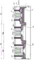
接下来,将沿着图3所示的工艺流程(步骤S1至S8)并且参考图4至15来描述本第一实施例的半导体器件的制造方法。Next, the manufacturing method of the semiconductor device of the present first embodiment will be described along the process flow shown in FIG. 3 (steps S1 to S8 ) and with reference to FIGS. 4 to 15 .
1.SOI衬底的制备(步骤S1)1. Preparation of SOI substrate (step S1)
首先,作为图3的步骤S1,制备SOI衬底1。在本实施例中,如图4所示,关于上述SOI衬底(衬底)1,器件隔离部分ST被埋入穿透半导体层SM和绝缘层BX并且到达半导体基底材料SB的沟槽TR中。在本第一实施例中,例如,半导体基底材料SB由p型单晶硅制成,并且半导体基底材料SB的厚度为250μm至800μm。然而,由n型单晶硅制成的半导体基底材料SB也可以被用作半导体基底材料SB。例如,绝缘层BX由氧化硅制成并且具有5nm至20nm的厚度。例如,半导体层SM由单晶硅制成,并且半导体层SM的厚度例如为5nm至20nm。此外,例如,元件隔离部分ST由氧化硅制成。在此,即使不通过例如离子注入将n型或p型杂质引入半导体层SM中,或者即使通过离子注入将杂质引入半导体层SM中,半导体层SM的杂质浓度也在1×10¹³/cm3或以下。在制备具有半导体基底材料SB、绝缘层BX和半导体层SM的SOI衬底1之后,形成沟槽TR和元件隔离部分ST,但是省略了对形成沟槽TR和元件隔离部分ST的方法的描述。First, as step S1 of FIG. 3 ,
如图4所示,SOI衬底1包括其中形成有第一MISFET的所谓的SOI区域1A、以及其中形成有第二MISFET和第三MISFET的所谓的体区1B。此外,体区1B包括其中形成有第二MISFET的第一区域1Ba、以及其中形成有第三MISFET的第二区域1Bb。As shown in FIG. 4 , the
2.体区的形成(步骤S2)2. Formation of the body region (step S2)
接下来,作为图3中的步骤S2,如图5所示,位于体区1B中的半导体层SM和位于体区1B中的绝缘层BX被去除,使得位于SOI区域1A中的半导体层SM和位于SOI区域1A中的绝缘层BX中的每个都没有被去除。具体地,在位于SOI区域1A中的半导体层SM上形成光致抗蚀剂图案(抗蚀剂图案、掩模层)(未示出),并且使用光致抗蚀剂图案覆盖SOI区域1A。使用光致抗蚀剂图案作为蚀刻掩模,对位于体区1B(1Ba、1Bb)中的半导体层SM进行蚀刻以去除位于体区1B(1Ba、1Bb)中的半导体层SM。结果,位于体区1B(1Ba和1Bb)中的绝缘层BX被暴露。另一方面,由于SOI区域1A被光致抗蚀剂图案(未示出)覆盖,所以位于SOI区域1A上的半导体层SM没有被去除。在本第一实施例中,例如,基于氟自由基的各向同性干法蚀刻被用作为蚀刻工艺。作为蚀刻气体,例如,SF6(六氟化硫)气体被使用。此外,在本第一实施例中,由于其中绝缘层BX和器件隔离部分ST中的每个的蚀刻速率低于半导体层SM的蚀刻速率的蚀刻条件被使用,因此通过半导体层SM的去除而暴露的绝缘层BX可以用作蚀刻停止层。Next, as step S2 in FIG. 3 , as shown in FIG. 5 , the semiconductor layer SM in the
在去除覆盖位于SOI区域1A中的半导体层SM的光致抗蚀剂图案之后,在使用新的光致抗蚀剂图案(未示出)覆盖体区1B的同时执行到位于SOI区域1A中的半导体基底材料SB中的离子注入。结果,如图5所示,在位于SOI区域1A中的半导体基底材料SB中形成半导体区域GPs。半导体区域GP是p型或n型半导体区域,并且被形成在与位于SOI区域1A中的绝缘层BX相邻的位置处。半导体区域GP被形成,以控制形成在SOI区域1A中的MISFET的阈值电压。具体地,在所制造的半导体器件中,通过向半导体区域GP施加预定电压,形成在SOI区域1A中的MISFET的阈值电压可以被控制。After removing the photoresist pattern covering the semiconductor layer SM located in the
之后,当在SOI区域1A中形成半导体区域GP时覆盖体区1B的光致抗蚀剂图案被去除,并且使用新的光致抗蚀剂图案(未示出)覆盖SOI区域1A。然后,使用覆盖SOI区域1A的光致抗蚀剂图案作为掩模(离子注入阻挡掩模),将杂质注入到位于体区1B中的半导体基底材料SB中。结果,如图5所示,在与位于体区1B中的绝缘层BX相邻的位置处形成阱WEL。在本第一实施例中,例如使用硼作为杂质。也就是说,在与位于体区1B中的绝缘层BX邻接的位置处形成的阱WEL是p型阱。After that, the photoresist pattern covering the
之后,覆盖SOI区域的1A的光致抗蚀剂图案被去除。然后,位于体区1B(1Ba、1Bb)中的绝缘层BX被蚀刻,以去除位于体区1B(1Ba、1Bb)中的绝缘层BX。结果,得到图5所示的状态。在本第一实施例中,例如,湿法蚀刻(各向同性蚀刻)被用作为蚀刻处理。After that, the photoresist pattern of 1A covering the SOI region is removed. Then, the insulating layer BX located in the
3.抬升过程(步骤S3)3. Lifting process (step S3)
接下来,作为图3的步骤S3,SOI区域1A和体区1B的第二区域1Bb覆盖有保护膜(未示出),使得体区1B的第一区域1Ba被暴露。然后,在体区1B的第一区域1Ba上执行外延生长以在位于第一区域1Ba中的半导体基底材料SB的表面SBaa(通过去除绝缘层BX而暴露的半导体基底材料SB的表面)上形成外延生长层EP1,如图6所示。也就是说,位于体区1B的第一区域1Ba中的半导体基底材料SB的上表面SBaa被抬升(在下文中也被称为“抬升处理”)。在本第一实施例中,如图6所示,外延生长处理被执行,使得外延生长层EP1的上表面EP1a位于与位于SOI区域1A中的半导体层SM的上表面SMa基本相同的高度。具体地,外延生长处理被执行,使得外延生长层EP1的上表面EP1a位于比位于体区1B的第二区域1Bb中的半导体基底材料SB的上表面SBab高的高度。外延生长处理被执行,使得外延生长层EP1的上表面EP1a位于与位于SOI区域1A中的半导体层SM的上表面SMa相同的高度或比位于SOI区域1A中的半导体层SM的上表面SMa低的高度。稍后将描述其原因。Next, as step S3 of FIG. 3 , the
此外,如上所述,在本第一实施例中,由于外延生长处理被执行,使得外延生长层EP1的上表面EP1a位于与位于SOI区域1A中的半导体层SM的上表面SMa基本相同的高度,所以通过本工艺形成的外延生长层EP1的厚度与位于SOI区域1A中的半导体层SM的厚度和位于SOI区域1A中的绝缘层BX的厚度之和基本相同。在该步骤中形成的外延生长层EP1的厚度比绝缘层BX和半导体层SM中的每个的厚度厚,例如10nm至40nm。Furthermore, as described above, in the present first embodiment, since the epitaxial growth process is performed so that the upper surface EP1a of the epitaxial growth layer EP1 is located at substantially the same height as the upper surface SMa of the semiconductor layer SM located in the
在该步骤中形成的外延生长层EP1由与组成基底材料SB的材料相同的材料制成。也就是说,在本第一实施例中,由于半导体基底材料SB由单晶硅构成,因此在该步骤中形成的外延生长层EP1也由例如单晶硅构成。The epitaxial growth layer EP1 formed in this step is made of the same material as that constituting the base material SB. That is, in the present first embodiment, since the semiconductor base material SB is composed of single crystal silicon, the epitaxial growth layer EP1 formed in this step is also composed of, for example, single crystal silicon.
在体区1B的第一区域1Ba中形成外延生长层EP1之后,杂质被注入到外延生长层EP1中。结果,如图6所示,在外延生长层EP1中形成阱(半导体区域和杂质区域)WEL。在此,被注入到外延生长层EP1中的杂质的种类与在先前的步骤中被注入到位于体区1B中的半导体基底材料SB中的杂质的种类相同。这是因为,形成在第一区域1Ba中的MISFET沟道区域由形成在第一区域1Ba中的阱WEL和形成在外延生长层EP1中的阱WEL组成。之后,覆盖SOI区域1A和体区1B的第二区域1Bb的保护膜(未示出)被去除。After the epitaxial growth layer EP1 is formed in the first region 1Ba of the
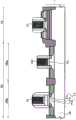
4.栅电极的形成4. Formation of the gate electrode
接下来,作为图3中的步骤S4,在区域1A和1B(1Ba和1Bb)中形成栅电极。具体地,如图8所示,经由栅极绝缘膜IF1在位于SOI区域1A中的半导体层SM的表面SMa上形成栅电极G1,经由栅极绝缘膜IF2在位于体区1B的第一区域1Ba中的外延生长层EP1的表面EP1a上形成栅电极G2,并且经由栅极绝缘膜IF3在位于体区1B的第二区域1Bb中的半导体基底材料SB的表面SBab上形成栅电极G3。栅电极G1、G2和G3中的每个的厚度为例如30nm至200nm。更具体地,在以下过程中形成栅电极G1、G2和G3中的每个。Next, as step S4 in FIG. 3, gate electrodes are formed in the
首先,如图7所示,通过例如CVD(化学气相沉积)方法经由氧化硅膜IF在包括区域1A、1B(1Ba、1Bb)和器件隔离部分ST的半导体基底材料SB上沉积多晶硅膜(或掺杂的多晶硅膜)PS。在此,在第二区域1Bb中,在将绝缘膜IF沉积在半导体基底材料SB上之前,稍后描述的绝缘层IF3a、IF3b被预先形成。之后,通过干法蚀刻对沉积的多晶硅膜PS进行图案化。也通过蚀刻对氧化硅IF进行图案化。结果,如图8所示,在区域1A和1B、1Ba和1Bb中形成栅电极G1、G2和G3以及栅极绝缘膜IF1、栅极绝缘膜IF2和栅极绝缘膜IF3。也就是说,在本第一实施例中,通过一个CVD工艺形成栅电极G1、G2和G3。栅电极G1、G2和G3由相同的材料、即多晶硅制成。First, as shown in FIG. 7, a polysilicon film (or doped silicon film) is deposited on a semiconductor base material
栅极绝缘膜IF1和栅极绝缘膜IF2均由氧化硅制成。另一方面,如图8所示,栅极绝缘膜IF3具有三层结构。具体地,栅极绝缘膜IF3被形成在位于体区1B的第二区域1Bb中的半导体基底材料SB的表面SBab上,并且具有由氧化硅制成的绝缘层IF3a、由氮化硅制成并且形成在绝缘层IF3a上的绝缘层IF3b、以及由氧化硅制成并且形成在绝缘层IF3b上的绝缘层IF3c。也就是说,绝缘层IF3b夹在两个绝缘层IF3a和IF3c之间,并且用作用于限制电荷的电荷保持层。Both the gate insulating film IF1 and the gate insulating film IF2 are made of silicon oxide. On the other hand, as shown in FIG. 8 , the gate insulating film IF3 has a three-layer structure. Specifically, the gate insulating film IF3 is formed on the surface SBab of the semiconductor base material SB in the second region 1Bb of the
栅极绝缘膜IF1、栅极绝缘膜IF2、绝缘层IF3a和绝缘层IF3c中的每个的厚度为例如2nm至4nm。另一方面,绝缘层IF3b的厚度例如为5nm至13nm。也就是说,由三个绝缘层IF3a、IF3b和IF3c组成的栅极绝缘膜IF3的厚度为9nm至21nm,并且比栅极绝缘膜IF1的厚度和栅极绝缘膜IF2的厚度厚。在本第一实施例中,在先前的步骤中,对位于体区1B的第一区域1Ba中的半导体基底材料SB执行外延生长处理。因此,如图8所示,由于栅极绝缘膜IF1、栅极绝缘膜IF2和栅极绝缘膜IF3(IF3c)的上表面位置位于基本相同的高度,因此栅电极G1、G2和G3的表面(上表面)也可以位于基本相同的高度。The thickness of each of the gate insulating film IF1, the gate insulating film IF2, the insulating layer IF3a, and the insulating layer IF3c is, for example, 2 nm to 4 nm. On the other hand, the thickness of the insulating layer IF3b is, for example, 5 nm to 13 nm. That is, the thickness of the gate insulating film IF3 composed of the three insulating layers IF3a, IF3b, and IF3c is 9 nm to 21 nm, and is thicker than the thicknesses of the gate insulating film IF1 and the gate insulating film IF2. In the present first embodiment, in the previous step, the epitaxial growth process is performed on the semiconductor base material SB located in the first region 1Ba of the
5.源极/漏极的形成(步骤S5)5. Formation of source/drain (step S5)
接下来,在每个区域1A和1B(1Ba、1Bb)中形成包括形成在SOI区域1A和体区1B(1Ba、1Bb)中的每个中的MISFET的将要用作源极/漏极的半导体区域(杂质区域)。如图9所示,用作源极/漏极的每个半导体区域包括半导体区域(杂质区域)EX、LDD和LMD、以及与半导体区域EX、LDD和LMD接触并且杂质浓度高于半导体区域EX、LDD和LMD的杂质浓度的半导体区域(杂质区域)D1、D2和MD。在形成偏移间隔物OS1、偏移间隔物OS2和低浓度半导体区域OS3之后并且在形成侧壁间隔物SW1、侧壁间隔物SW2和侧壁间隔物SW3之前,形成低浓度半导体区域EX、LDD和LMD。此外,在形成侧壁间隔物SW1、侧壁间隔物SW2和侧壁间隔物SW3之后,形成高浓度半导体区域D1、D2和MD。下面将详细描述在各个区域1A和1B中形成的源极/漏极区域。Next, a semiconductor to be used as source/drain including the MISFET formed in each of the
首先,如图9所示,形成在SOI区域1A中的源极/漏极在半导体层SM中包括被形成为覆盖栅电极G1的侧面的偏移间隔物(绝缘膜)OS1、形成在用被形成为覆盖偏移间隔物OS1的侧壁(绝缘膜)SW1覆盖的一部分(位置)中的半导体区域(延伸区域)EX、以及形成在从偏移间隔物OS1和侧壁SW1暴露的半导体层SM的一部分(位置)中的半导体区域(扩散区域)D1。First, as shown in FIG. 9 , the source/drain formed in the
在此,位于SOI区域1A中的半导体层SM的一部分(其位于栅电极G1的正下方,并且在作为源极的半导体层SM与作为漏极的半导体层之间)作为形成在SOI区域1A中的MISFET的沟道区域。在本第一实施例中,构成沟道区域的半导体层SM的厚度小至5nm至20nm。因此,当在稍后的步骤中在将要作为源极/漏极的半导体区域上形成接触孔时,有可能接触孔被形成以使得接触孔的底部到达位于半导体层SM下方的绝缘层BX或位于绝缘层BX下方的半导体基底材料SB。Here, a part of the semiconductor layer SM located in the
因此,在本第一实施例中,如图9所示,在从栅电极G1和偏移间隔物OS1暴露的半导体层SM上执行外延生长处理,并且在从栅电极G1和偏移间隔物OS1暴露的半导体层SM的表面SMa上形成外延生长层EP2。杂质也被注入到所形成的外延生长层EP2中。也就是说,如图9所示,构成形成在SOI区域1A中的源极/漏极的半导体区域D1包括形成在半导体层SM中的部分和形成在外延生长层EP2(该外延生长层EP2形成在半导体层SM上的)中的部分。Therefore, in the present first embodiment, as shown in FIG. 9 , epitaxial growth processing is performed on the semiconductor layer SM exposed from the gate electrode G1 and the offset spacer OS1 , and an epitaxial growth process is performed on the semiconductor layer SM exposed from the gate electrode G1 and the offset spacer OS1 . An epitaxial growth layer EP2 is formed on the surface SMa of the exposed semiconductor layer SM. Impurities are also implanted into the formed epitaxial growth layer EP2. That is, as shown in FIG. 9 , the semiconductor region D1 constituting the source/drain formed in the
如图9所示,形成在体区1B的第一区域1Ba中的源极/漏极包括被形成为覆盖在外延生长层EP1中的栅电极G2的侧面的偏移间隔物OS2、形成在用被形成为覆盖偏移间隔物OS2的侧壁SW2覆盖的一部分(位置)中的半导体区域(杂质区域)LDD、以及在从外延生长层EP1中的偏移间隔物OS2和侧壁SW2暴露的一部分(位置)中形成的半导体区域(扩散区域)D2。此外,如图9所示,形成在体区1B的第二区域1Bb中的源极/漏极包括半导体区域(杂质区域)LMD和半导体区域(扩散区域)MD,该所述半导体区域(杂质区域)LMD形成在用被形成为覆盖栅电极G3的侧面的偏移间隔物OS3和被形成为覆盖偏移间隔物OS3的侧壁SW3覆盖的半导体基底材料SB的一部分(位置)中,该半导体区域(扩散区域)MD形成在从偏移间隔物OS3和侧壁SW3暴露的半导体基底材料SB的一部分(位置)中。As shown in FIG. 9, the source/drain formed in the first region 1Ba of the
注意,如果要形成的MISFET是n型场效应晶体管,则用于形成用作源极/漏极的半导体区域(延伸区域、杂质区域和扩散区域)的杂质是诸如磷(P)或砷(As)等n型杂质。另一方面,如果要形成的MISFET是p型场效应晶体管,则用于形成各个半导体区域(延伸区域、杂质区域和扩散区域)的杂质是诸如硼(B)等p型杂质。Note that if the MISFET to be formed is an n-type field effect transistor, the impurities used to form the semiconductor regions (extension regions, impurity regions, and diffusion regions) serving as source/drain are such as phosphorus (P) or arsenic (As ) and other n-type impurities. On the other hand, if the MISFET to be formed is a p-type field effect transistor, the impurities for forming the respective semiconductor regions (extension regions, impurity regions and diffusion regions) are p-type impurities such as boron (B).
在形成构成每个MISFET的源极/漏极的半导体区域之后,在构成每个MISFET的源极/漏极的半导体区域D1、D2和MD的表面EP2a、EP1a和SBab的表面上形成硅化物膜SLF1、SLF2和SLF3,如图9所示。After forming the semiconductor regions constituting the source/drain of each MISFET, a silicide film is formed on the surfaces of the surfaces EP2a, EP1a and SBab of the semiconductor regions D1, D2 and MD constituting the source/drain of each MISFET SLF1, SLF2, and SLF3, as shown in Figure 9.
6.中间绝缘膜的形成(步骤S6)6. Formation of intermediate insulating film (step S6)
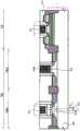
接下来,作为图3的步骤S6,在衬底1上形成层间绝缘膜IL以覆盖形成在区域1A和1B(1Ba和1Bb)中的栅电极G1、G2和G3。在此,如图10所示,由于栅电极G1、G2和G3从衬底1的表面向上突出,所以根据所形成的栅电极G1、G2和G3的厚度(高度),在层间绝缘膜IL的表面上形成凹凸。也就是说,在层间绝缘膜IL中的栅电极G1、G2和G3上形成凸部部分P1、P2和P3。Next, as step S6 of FIG. 3 , an interlayer insulating film IL is formed on the
7.抛光(步骤S7)7. Polishing (step S7)
接下来,作为图3的步骤S7,层间绝缘膜1L的一部分被抛光。在此,当具有由多晶硅膜制成的栅电极的MISFET被制造时,层间绝缘膜IL的抛光量被控制,使得栅电极不被暴露。另一方面,本第一实施例中的半导体器件的制造方法形成了具有由金属材料制成的栅电极的MISFET。因此,在本第一实施例中,如图11所示,层间绝缘膜IL被抛光,使得形成在区域1A和1B(1Ba和1Bb)中的栅电极G1、G2和G3从层间绝缘膜IL暴露。然后,通过本抛光步骤形成进行抛光步骤的层间绝缘膜IL1。此后,用不同于多晶硅膜的金属材料来替换构成栅电极G1、G2和G3中的每个的材料的步骤被执行。Next, as step S7 of FIG. 3 , a part of the interlayer insulating film 1L is polished. Here, when a MISFET having a gate electrode made of a polysilicon film is manufactured, the polishing amount of the interlayer insulating film IL is controlled so that the gate electrode is not exposed. On the other hand, the manufacturing method of the semiconductor device in the present first embodiment forms a MISFET having a gate electrode made of a metal material. Therefore, in the present first embodiment, as shown in FIG. 11, the interlayer insulating film IL is polished so that the gate electrodes G1, G2, and G3 formed in the
8.栅电极的置换过程(步骤S8)8. Gate electrode replacement process (step S8)
接下来,作为图3的步骤S8,将描述组成栅电极的材料的置换过程。Next, as step S8 of FIG. 3 , a replacement process of the material constituting the gate electrode will be described.
首先,对从抛光的层间绝缘膜IL1暴露的栅电极G1、G2和G3进行例如湿法蚀刻工艺以去除栅电极G1、G2和G3。结果,如图12所示,在由一对偏移间隔物OS1、OS2和OS3以及栅极绝缘膜IF1、栅极绝缘膜IF2、栅极绝缘膜IF3(IF3c)围绕的区域中形成间隙GAP1、GAP2和GAP3。First, the gate electrodes G1 , G2 and G3 exposed from the polished interlayer insulating film IL1 are subjected to, for example, a wet etching process to remove the gate electrodes G1 , G2 and G3 . As a result, as shown in FIG. 12, gaps GAP1, GAP1, IF3 are formed in regions surrounded by the pair of offset spacers OS1, OS2, and OS3 and the gate insulating film IF1, gate insulating film IF2, and gate insulating film IF3 (IF3c). GAP2 and GAP3.
接下来,如图13所示,金属膜MF被形成在抛光的层间绝缘膜IL1上以阻挡图12中描述的区域1A和1B(1Ba和1Bb)的间隙GAP1、GAP2和GAP3。在此,通过例如溅射形成金属膜MF。金属膜MF由例如氮化钛制成。此外,尽管未示出,但是金属膜MF经由例如由基于氧化铪的高介电常数材料制成的栅极绝缘膜(高k栅极绝缘膜)而被形成在抛光的层间绝缘膜IL1、偏移间隔物OS1、OS2和OS3、以及栅极绝缘膜IF1、IF2和IF3上。高k栅极绝缘膜(HfON、HfO)由例如ALCVD(原子层化学气相沉积)形成。高介电常数栅极绝缘膜的厚度为例如几埃至几十埃。Next, as shown in FIG. 13 , a metal film MF is formed on the polished interlayer insulating film IL1 to block the gaps GAP1 , GAP2 and GAP3 of the
然后,如图14所示,通过去除图12中描述的位于间隙GAP1、GAP2和GAP3外部的金属膜MF(和高k栅极绝缘膜)的部分(即,位于抛光的层间绝缘膜1L1的表面上的金属膜MF的不必要的部分)来形成由金属材料制成的栅电极(金属栅电极)MTG1、MTG2和MTG3。在本第一实施例中,通过例如抛光来去除不必要的部分。Then, as shown in FIG. 14 , by removing the portion of the metal film MF (and the high-k gate insulating film) located outside the gaps GAP1 , GAP2 , and GAP3 described in FIG. 12 (ie, located on the polished interlayer insulating film 1L1 ) unnecessary portions of the metal film MF on the surface) to form gate electrodes (metal gate electrodes) MTG1, MTG2, and MTG3 made of a metal material. In the present first embodiment, unnecessary portions are removed by, for example, polishing.
接下来,如图15所示,另一层间绝缘膜IL2被形成在抛光的层间绝缘膜IL1上,以覆盖从抛光的层间绝缘膜IL1暴露的金属栅电极MTG1、MTG2和MTG3的暴露部分。在层间绝缘膜IL1和IL2中在与用作分别具有金属栅电极MTG1、MTG2和MTG3的场效应晶体管(MISFET和MOSFET)Q1、Q2和Q3的源极和漏极的半导体区域D1、D2和MD交叠的位置处形成接触孔CH1、CH2和CH3。接触孔CH1、接触孔CH2和接触孔CH3通过例如光刻和干法蚀刻来形成。然后,将由例如钨制成的导电膜掩埋在接触孔CH1、CH2和CH3中,从而形成如图15所示的接触插塞CP1、CP2和CP3。之后,在位于层间绝缘膜IL2上的布线层ML1上形成多个布线(布线图案)M1,并且用层间绝缘膜IL3覆盖多个布线M1,从而得到图2所示的状态。Next, as shown in FIG. 15, another interlayer insulating film IL2 is formed on the polished interlayer insulating film IL1 to cover the exposure of the metal gate electrodes MTG1, MTG2 and MTG3 exposed from the polished interlayer insulating film IL1 part. In the interlayer insulating films IL1 and IL2, in the interlayer insulating films IL1 and IL2, the semiconductor regions D1, D2, and Contact holes CH1 , CH2 and CH3 are formed at positions where the MDs overlap. The contact hole CH1, the contact hole CH2, and the contact hole CH3 are formed by, for example, photolithography and dry etching. Then, a conductive film made of, for example, tungsten is buried in the contact holes CH1 , CH2 and CH3 , thereby forming contact plugs CP1 , CP2 and CP3 as shown in FIG. 15 . After that, a plurality of wirings (wiring patterns) M1 are formed on the wiring layer ML1 on the interlayer insulating film IL2, and the plurality of wirings M1 are covered with the interlayer insulating film IL3, thereby obtaining the state shown in FIG. 2 .
(第一实施例的制造半导体器件的方法的效果)(Effect of the method of manufacturing a semiconductor device of the first embodiment)
接下来,将结合几个检查示例来描述本第一实施例的制造半导体器件的方法的效果。Next, the effects of the method of manufacturing a semiconductor device of the present first embodiment will be described with reference to several inspection examples.
(检查示例1)(check example 1)
首先,如上所述,构成本第一实施例的半导体器件的衬底不仅包括具有形成在半导体基底材料上的绝缘层和半导体层的SOI区域(例如,SOI区域1A),而且还包括既不具有绝缘层也不具有半导体层的体区(例如,体区1B)。体区包括其中形成有包括具有第一厚度的栅极绝缘膜(例如,栅极绝缘膜IF2)的MISFET的区域(例如,第一区域1Ba)、以及其中形成有包括具有大于第一厚度的厚度的第二栅极绝缘膜(例如,栅极绝缘膜IF3)的MISFET的区域(例如,第二区域1Bb)。到此为止的配置在图16中示出为检查示例1。First, as described above, the substrate constituting the semiconductor device of the present first embodiment includes not only the SOI region (for example, the
另一方面,如上所述,在本第一实施例的半导体器件的制造方法中,首先,形成临时栅电极,然后依次形成偏移间隔物和侧壁以覆盖栅电极的侧壁。在要形成MISFET的区域、即有源区域中形成用作源极/漏极区域的半导体区域,然后用层间绝缘膜覆盖临时栅电极。然后,在去除层间绝缘膜的一部分以暴露临时栅电极的一部分之后,在通过去除临时栅电极而形成的间隙中埋入与构成临时栅电极的材料(例如,多晶硅膜)不同的材料(例如,金属膜)。也就是说,本第一实施例的半导体器件的制造方法是所谓的后栅极工艺。On the other hand, as described above, in the manufacturing method of the semiconductor device of the present first embodiment, first, the temporary gate electrode is formed, and then the offset spacer and the sidewall are sequentially formed to cover the sidewall of the gate electrode. A semiconductor region serving as a source/drain region is formed in a region where the MISFET is to be formed, that is, an active region, and then a temporary gate electrode is covered with an interlayer insulating film. Then, after removing a part of the interlayer insulating film to expose a part of the temporary gate electrode, a material (eg, a polysilicon film) different from a material constituting the temporary gate electrode (eg, a polysilicon film) is buried in the gap formed by removing the temporary gate electrode , metal film). That is, the manufacturing method of the semiconductor device of the present first embodiment is a so-called gate-last process.
在此,如图16所示,在检查示例1中,由于未在体区1B中的第一区域1Ba上执行外延生长处理,因此栅电极G1、G2a和G3的表面(上表面)没有位于基本相同的高度。具体地,形成在体区1B中的第一区域1Ba中的栅电极G2a的表面低于形成在其他区域1A和1Bb中的栅电极G1和G3的表面。因此,在这种配置中,当层间绝缘膜IL1被抛光以使得形成在区域1A和1B(1Ba和1Bb)中的所有栅电极G1、G2a和G3都从层间绝缘膜IL1暴露时,对栅电极G1和G3进行了不必要的抛光(去除),如图17所示。结果,由稍后的替换工艺形成的金属栅电极可能不具有期望形式(厚度),并且电特性(即,半导体器件的可靠性)可能劣化。Here, as shown in FIG. 16 , in Inspection Example 1, since the epitaxial growth process is not performed on the first region 1Ba in the
(检查示例2)(check example 2)
本发明人还研究了当从栅电极G2a突出到衬底1上方的栅电极G1和G3被暴露时,其中层间绝缘膜IL1的抛光被终止的检查示例2。然而,在检查示例2中,如图18所示,在所有栅电极G1、G2a和G3中,其上表面最靠近构成衬底1的半导体基底材料SB的栅电极G2a没有从层间绝缘膜IL1暴露。结果,构成栅电极G2a的材料(例如,多晶硅膜)不能被另一种材料(例如,金属膜)替换。也就是说,难以提高包括栅电极G2a的电路的处理速度。The present inventors also studied inspection example 2 in which polishing of the interlayer insulating film IL1 was terminated when the gate electrodes G1 and G3 protruding from the gate electrode G2a over the
(检查示例3)(check example 3)
因此,本发明人研究了采用比栅电极G2a的高度(厚度)高(厚)的栅电极G2b作为新的检查示例。结果,如图19所示,可以从层间绝缘膜IL1暴露栅电极G1、G2b和G3,而没有不必要地抛光或去除栅电极G1、G2b和G3。但是,在本检查示例3中,如图20所示,通过在栅电极G2b上执行置换步骤的一部分而形成的间隙GAP2b的纵横比(H2/L2)变为大于在检查示例1中通过在栅电极G2a上执行置换步骤的一部分而形成的间隙的纵横比(H1/L1),即,通过在其他栅电极上执行置换步骤的一部分而形成的间隙的纵横比(OOF)。结果,在所形成的间隙GAP2b中埋入金属膜变得困难。也就是说,所形成的金属栅电极可能具有空隙,这会降低半导体器件的可靠性。Therefore, the present inventors studied the use of the gate electrode G2b higher (thicker) than the height (thickness) of the gate electrode G2a as a new inspection example. As a result, as shown in FIG. 19, the gate electrodes G1, G2b, and G3 can be exposed from the interlayer insulating film IL1 without unnecessary polishing or removal of the gate electrodes G1, G2b, and G3. However, in this inspection example 3, as shown in FIG. 20, the aspect ratio (H2/L2) of the gap GAP2b formed by performing a part of the replacement step on the gate electrode G2b becomes larger than that in the inspection example 1 by performing a part of the replacement step on the gate electrode G2b The aspect ratio (H1/L1) of the gap formed by performing part of the replacement step on electrode G2a, ie the aspect ratio (OOF) of the gap formed by performing part of the replacement step on other gate electrodes. As a result, it becomes difficult to bury the metal film in the formed gap GAP2b. That is, the formed metal gate electrode may have voids, which may reduce the reliability of the semiconductor device.
(检查示例4)(check example 4)
如上所述,构成本第一实施例的半导体器件的衬底不仅包括具有形成在半导体基底材料上的绝缘层和半导体层的SOI区域(例如,SOI区域1A),而且还包括不具有绝缘层和半导体层的体区(例如,体区1B)。也就是说,在横截面图中,形成在体区1B中的MISFET的栅电极的表面(上表面)低于形成在SOI区域1A中的MISFET的栅电极的表面(上表面)。因此,作为其他检查示例,本发明人已经考虑到,如图21所示,在去除位于体区1B中的半导体层和绝缘层之后,在所有体区1B(即第一区域1Ba和第二区域1Bb两者)上执行外延生长处理,从而减小由于去除半导体层和绝缘层两者而引起的水平差。换言之,外延生长处理在各个区域1Ba和1Bb上被执行,使得不仅外延生长层EP1的上表面EP1a而且外延生长层EP3的上表面EP1b都位于与位于SOI区域1A中的半导体层SM的上表面SMa基本相同的高度。As described above, the substrate constituting the semiconductor device of the present first embodiment includes not only the SOI region (for example, the
然而,如图21所示,形成在体区1B中的第二区域1Bb中的MISFET的栅极绝缘膜IF3的厚度比形成在其他区域1A和1Ba中的MISFET的栅极绝缘膜IF1和IF2的厚度厚。因此,与检查示例1和检查示例2相似地,在抛光步骤之前,各个栅电极G1、G2和G3的表面(上表面)不能位于基本相同的高度。However, as shown in FIG. 21 , the thickness of the gate insulating film IF3 of the MISFET formed in the second region 1Bb in the
相反,在本第一实施例中,如图2、6和15所示,在其中形成有具有薄栅极绝缘膜IF2的场效应晶体管(MISFET)Q2的体区1B的第一区域1Ba上执行外延生长处理,但是未在其中形成有具有厚栅极绝缘膜IF3的场效应晶体管(MISFET)Q3的体区1B的第二区域1Bb上执行外延生长处理。因此,如图8所示,在抛光层间绝缘膜IL的步骤之前,栅电极G1、G2和G3的表面(上表面)可以位于彼此基本相同的高度。结果,如图11至14所示,由于具有与预先形成的临时栅电极G1、G2和G3基本相同的形状(厚度)的金属栅电极MTG1、MTG2和MTG3可以被形成,因此可以抑制半导体器件的可靠性的劣化。换言之,由于具有期望形状的金属栅电极可以被用于各个MISFET,所以可以实现高速半导体器件。此外,在本第一实施例中,如上所述,在层间绝缘膜IL的抛光步骤之前,栅电极G1、G2和G3的表面(上表面)位于彼此基本相同的高度,因此,可以容易地设置后续抛光步骤中的抛光条件(抛光量)。也就是说,由于可以容易地以稳定的方式从抛光的层间绝缘膜IL1暴露所有栅电极,所以可以提高半导体器件的成品率。In contrast, in the present first embodiment, as shown in FIGS. 2 , 6 and 15 , on the first region 1Ba in which the
(第一实施例的修改示例)(Modified example of the first embodiment)
接下来,将描述本第一实施例的修改示例。Next, a modified example of the present first embodiment will be described.
(修改示例1)(modified example 1)
首先,在上述第一实施例中,如参考图5所述,位于体区1B中的半导体层SM被去除,离子被注入到位于SOI区域1A中的半导体基底材料SB中,离子被注入到位于体区1B中的半导体基底材料SB中,然后位于SOI区域1A和体区1B的每个中的绝缘层BX被去除。相反,在本第一修改示例中,首先,在位于体区1B中的半导体层SM被去除之后,离子被注入到位于体区1B中的半导体基底材料SB中,并且进一步,离子被注入到位于SOI区域1A中的半导体基底材料SB中,之后,位于SOI区域1A和体区1B中的每个中的绝缘层BX被去除。在上述第一实施例和第一修改示例中的每个中,在用于去除半导体层SM和绝缘层BX的蚀刻工艺中使用的光致抗蚀剂图案的类型与在离子注入工艺中使用的光致抗蚀剂图案的类型彼此不同。First, in the above-described first embodiment, as described with reference to FIG. 5 , the semiconductor layer SM located in the
(修改示例2)(modified example 2)
接下来,在上述第一实施例中,作为抬升处理中的具体示例,如参考图6所述,外延生长处理已经被描述,使得外延生长层EP1的上表面EP1a位于比位于体区1B中的第二区域1Bb中的半导体基底材料SB的上表面SBab高的高度,并且使得其位于与位于SOI区域1A中的半导体层SM的上表面SMa相同的高度,或者位于比位于SOI区域1A中的半导体层SM的上表面SMa低的高度。另一方面,在本第二修改示例中,外延生长处理被执行,使得外延生长层EP1的上表面EP1a位于比位于SOI区域1A中的半导体层SM的上表面SMa高的高度。然而,如果外延生长层EP1的上表面EP1a比半导体层SM的上表面SMa过高(厚),则不仅外延生长处理花费更长的时间,而且形成在第一区域1Ba中的栅电极G2a在稍后的抛光步骤中被不必要地抛光(去除)。因此,当难以控制外延生长以使得外延生长层EP1的上表面EP1a变为与半导体层SM的上表面SMa相同的高度时,优选地执行外延生长处理以使得外延生长层EP1的上表面EP1a位于与半导体层SM的上表面SMa相同的高度或比半导体层SM的上表面SMa低的高度,如在上述第一实施例中鉴于外延生长处理所需要的时间。Next, in the above-described first embodiment, as a specific example in the lift-up process, as described with reference to FIG. 6 , the epitaxial growth process has been described so that the upper surface EP1a of the epitaxial growth layer EP1 is located more than the upper surface EP1a of the epitaxial growth layer EP1 located in the
(修改示例3)(modified example 3)
接下来,在上述第一实施例中,如图5所示,阱WEL形成在与位于体区1B(具体地是第一区域1Ba)中的绝缘层BX相邻的位置处,对第一区域1Ba进行抬升处理(即,外延生长处理),然后在通过抬升工艺形成的外延生长层EP1中形成阱WEL。与此相对,在本第三修改示例中,在第一区域1Ba中,仅在执行抬升处理之后执行离子注入处理,而不在抬升处理之前执行离子注入处理。也就是说,当在体区1B的第二区域1Bb上执行离子注入时,第一区域1Ba被光致抗蚀剂图案覆盖。根据本第三修改示例,由于向第一区域1Ba中的离子注入的数目可以被减少,因此与第一实施例中的阈值电压相比,在第一区域1Ba中形成的第二场效应晶体管Q2的阈值电压的变化可以被减小。Next, in the above-described first embodiment, as shown in FIG. 5 , the well WEL is formed at a position adjacent to the insulating layer BX located in the
(修改示例4)(modified example 4)
接下来,在上述第一实施例中,形成在第二区域1Bb中并且构成闪存电路的场效应晶体管Q3具有栅极绝缘膜IF3,该栅极绝缘膜IF3包括由氧化硅制成的绝缘层IF3a、由氮化硅制成并且形成在绝缘层IF3a上的绝缘层IF3b、以及由氧化硅制成并且形成在绝缘层IF3b上的绝缘层IF3c。另一方面,本第四修改示例涉及作为构成另一存储电路的MISFET的铁电存储器。更具体地,本第四修改示例的MISFET的栅电极形成在位于第二区域1Bb中的半导体基底材料SB上,并且经由由氧化硅制成的绝缘层、由氧化硅制成并且包含铪的绝缘层(例如,HfSiO或HfZrO2)、以及由氮化钛制成并且形成在包含铪的绝缘层上的覆盖膜而被形成在半导体基底材料SB上。位于中央的包含铪的绝缘层是铁电膜。铁电膜是上述三层中最厚的。但是,铁电膜的最大厚度为约10nm,比第一实施例的绝缘层(电荷保持层、电荷存储层)IF3b的最大厚度(约13nm)薄。Next, in the above-described first embodiment, the field effect transistor Q3 formed in the second region 1Bb and constituting the flash memory circuit has the gate insulating film IF3 including the insulating layer IF3a made of silicon oxide , an insulating layer IF3b made of silicon nitride and formed on the insulating layer IF3a, and an insulating layer IF3c made of silicon oxide and formed on the insulating layer IF3b. On the other hand, the present fourth modified example relates to a ferroelectric memory as a MISFET constituting another memory circuit. More specifically, the gate electrode of the MISFET of the present fourth modification example is formed on the semiconductor base material SB in the second region 1Bb, and via an insulating layer made of silicon oxide, an insulating layer made of silicon oxide and containing hafnium A layer (for example, HfSiO or HfZrO2 ), and a capping film made of titanium nitride and formed on an insulating layer containing hafnium are formed on the semiconductor base material SB. The insulating layer containing hafnium at the center is a ferroelectric film. The ferroelectric film is the thickest of the three layers mentioned above. However, the maximum thickness of the ferroelectric film is about 10 nm, which is thinner than the maximum thickness (about 13 nm) of the insulating layer (charge holding layer, charge storage layer) IF3b of the first embodiment.
(修改示例5)(modified example 5)
此外,在上述第一实施例中,已经描述了具有三层栅极绝缘膜IF3的MISFET被形成在体区1B的第二区域1Bb中。与此相对,在本第五修改示例中,形成在第二区域1Bb中的MISFET的栅极绝缘膜被形成为一层。更具体地,如图22所示,在本第五修改示例的半导体器件SD2中,在体区1B的第一区域1Ba中形成有低击穿电压场效应晶体管(MISFET)Q4,并且在体区1B的第二区域1Bb中形成有高击穿电压场效应晶体管(MISFET)Q5。如图22所示,构成高击穿电压场效应晶体管Q5的栅极绝缘膜IF5的厚度比构成低击穿电压场效应晶体管Q4的栅极绝缘膜IF4的厚度厚。本第五修改示例中的栅极绝缘膜IF4的厚度为例如2nm至4nm。本第五修改示例中的栅极绝缘膜IF5的厚度为例如9nm至21nm。栅极绝缘膜IF4和IF5的厚度根据所需要的耐压而变化。因此,构成高击穿电压场效应晶体管的栅极绝缘膜的厚度可以是例如第一实施例的栅极绝缘膜IF3的厚度(9nm至21nm)的一半或更小。当这种高击穿电压型场效应晶体管的栅电极也要采用金属栅电极时,必须对其中形成有高击穿电压型场效应晶体管的区域(在此是第二区域1Bb)也执行抬升工艺。在本修改示例中,高击穿电压型场效应晶体管Q5的栅极绝缘膜IF5的厚度大于低击穿电压型场效应晶体管Q4的栅极绝缘膜IF4的厚度,但是高击穿电压型场效应晶体管Q5的栅极长度可以大于低击穿电压型场效应晶体管Q4的栅极长度。在此,“栅极长度”是栅电极的沿着从在图22中用作源极/漏极的两个半导体区域LDD中的一个半导体区域LDD到另一半导体区域LDD的方向的长度。另外,高击穿电压场效应晶体管Q5的栅极长度和栅极绝缘膜IF5的厚度可以分别大于低击穿电压场效应晶体管Q4的栅极长度和栅极绝缘膜IF4的厚度。注意,除了上述之外,构成栅极绝缘膜、金属栅电极、偏移间隔物、用作源极/漏极区域的半导体区域等的材料与上述第一实施例和每个修改示例中描述的相同,因此省略其描述。Furthermore, in the above-described first embodiment, it has been described that the MISFET having the three-layer gate insulating film IF3 is formed in the second region 1Bb of the
(第二实施例)(Second Embodiment)
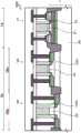
接下来,将参考23和24描述本第二实施例的半导体器件SD3。图23是本第二实施例的半导体器件SD3的示意图。图24是包括图23所示的多个存储单元MC之一的第二实施例的半导体器件的主要部分截面图。应当注意,与上述第一实施例的不同之处在于,首先,在上述第一实施例中,在作为体区1B中的一个有源区域的第二区域1Bb中形成一个(一种)场效应晶体管(MISFET)Q3,但是在本第二实施例中,如图23和24所示,在作为体区1B中的一个有源区域的第二区域1Bb中形成两个(两种)场效应晶体管(MISFET)Q3和Q6,这不同于上述第一实施例。其他结构与上述第一实施例和各个修改示例中描述的结构相同,因此省略其描述。Next, the semiconductor device SD3 of the second embodiment will be described with reference to 23 and 24 . FIG. 23 is a schematic diagram of the semiconductor device SD3 of the second embodiment. 24 is a main part cross-sectional view of the semiconductor device of the second embodiment including one of the plurality of memory cells MC shown in FIG. 23 . It should be noted that the difference from the above-described first embodiment is that, first, in the above-described first embodiment, one (a) field effect is formed in the second region 1Bb which is one active region in the
如图23所示,多个存储单元MC中的每个包括场效应晶体管(存储器晶体管)Q3、以及与场效应晶体管Q3串联连接并且控制(选择)场效应晶体管Q3的场效应晶体管(选择晶体管)Q6。场效应晶体管Q3的栅电极(金属栅电极MTG3)电连接到相应的存储栅线(字线)MGL0和MGL1。也就是说,场效应晶体管Q3的栅电极是存储器栅电极MG。另一方面,场效应晶体管Q6的栅电极(金属栅电极MTG6)电连接到相应的控制栅线(选择栅线)CGL0和CGL1。也就是说,场效应晶体管Q6的栅电极是控制栅电极(选择栅电极)CG。场效应晶体管Q3的源极/漏极电连接到位线BL0和BL1。场效应晶体管Q6的源极/漏极电连接到源极线SL0和SL1。As shown in FIG. 23, each of the plurality of memory cells MC includes a field effect transistor (memory transistor) Q3, and a field effect transistor (selection transistor) that is connected in series with the field effect transistor Q3 and controls (selects) the field effect transistor Q3 Q6. The gate electrode (metal gate electrode MTG3) of the field effect transistor Q3 is electrically connected to the corresponding memory gate lines (word lines) MGL0 and MGL1. That is, the gate electrode of the field effect transistor Q3 is the memory gate electrode MG. On the other hand, the gate electrode (metal gate electrode MTG6) of the field effect transistor Q6 is electrically connected to the corresponding control gate lines (selection gate lines) CGL0 and CGL1. That is, the gate electrode of the field effect transistor Q6 is the control gate electrode (selection gate electrode) CG. The source/drain of the field effect transistor Q3 is electrically connected to the bit lines BL0 and BL1. The source/drain of the field effect transistor Q6 is electrically connected to the source lines SL0 and SL1.
如图24所示,本第二实施例的半导体器件具有在其中形成有存储晶体管Q3的存储晶体管形成区域(存储晶体管形成部分)1Bba和其中在体区1B的第二区域1Bb中形成有选择晶体管Q6的选择晶体管形成区域(选择晶体管形成部分)1Bbb上方延伸的公共半导体区域(扩散区域、杂质区域)CMD。具体地,公共半导体区域CMD被形成在位于存储晶体管形成区域1Bba中的半导体基底材料SB和形成在位于控制晶体管形成区域1Bbb中的半导体基底材料SB上的外延生长层EP4两者中。也就是说,公共半导体区域CMD是用作场效应晶体管Q3的漏极的半导体区域(扩散区域、杂质区域),并且也是用作场效应晶体管Q6的源极的半导体区域(扩散区域、杂质区域)。As shown in FIG. 24 , the semiconductor device of the present second embodiment has a memory transistor formation region (memory transistor formation portion) 1Bba in which the memory transistor Q3 is formed and a selection transistor in which the selection transistor is formed in the second region 1Bb of the
在本第二实施例中,如图24所示,控制晶体管Q6的栅极绝缘膜IF6的厚度小于存储晶体管Q3的栅极绝缘膜IF3的厚度。也就是说,控制晶体管Q6的栅极绝缘膜IF6的厚度为例如2nm至8nm。因此,如图24所示,外延生长层EP4被形成在位于第二区域1Bb的选择晶体管形成区域1Bbb中的半导体基底材料SB上。顺便提及,以与上述第一实施例相同的方式,杂质被注入到形成在控制晶体管形成区域1Bbb中的外延生长层EP4中。换言之,阱(半导体区域和杂质区域)WEL也被形成在外延生长层EP4中。In the second embodiment, as shown in FIG. 24, the thickness of the gate insulating film IF6 of the control transistor Q6 is smaller than the thickness of the gate insulating film IF3 of the memory transistor Q3. That is, the thickness of the gate insulating film IF6 of the control transistor Q6 is, for example, 2 nm to 8 nm. Therefore, as shown in FIG. 24 , the epitaxial growth layer EP4 is formed on the semiconductor base material SB located in the selection transistor forming region 1Bbb of the second region 1Bb. Incidentally, in the same manner as in the above-described first embodiment, impurities are implanted into the epitaxial growth layer EP4 formed in the control transistor formation region 1Bbb. In other words, the well (semiconductor region and impurity region) WEL is also formed in the epitaxial growth layer EP4.
例如,当在图3的工艺流程中所示的步骤S3(抬升处理)中在体区1B的第一区域1Ba上执行外延生长处理时,通过在选择晶体管形成区域1Bbb上也执行外延生长处理来形成在选择晶体管形成区域1Bbb中形成的外延生长层EP4。然而,可以在与用于第一区域1Ba的外延生长处理不同的步骤中执行用于选择晶体管形成区域1Bbb的外延生长处理。For example, when the epitaxial growth process is performed on the first region 1Ba of the
(制造第二实施例的半导体器件的方法的效果)(Effect of the method of manufacturing the semiconductor device of the second embodiment)
接下来,将描述制造本第二实施例的半导体器件的方法的效果。Next, the effects of the method of manufacturing the semiconductor device of the second embodiment will be described.
在本第二实施例中,如图24所示,在体区1B中,在其中形成有具有薄栅极绝缘膜IF2的场效应晶体管(MISFET)Q2的第一区域1Ba以及其中形成有具有相同的薄栅极绝缘膜IF6的场效应晶体管(MISFET)Q6的选择晶体管形成区域1Bbb上执行外延生长处理,但是在选择晶体管形成区域1Bbb上不执行外延生长处理,在选择晶体管形成区域1Bbb中,具有厚栅极绝缘膜IF3的场效应晶体管(MISFET)Q3被形成在体区1B中。因此,在抛光层间绝缘膜IL的步骤之前,形成在区域1A、1Ba、1Bba和1Bbb中的栅电极的表面(上表面)可以位于彼此基本相同的高度,如上述第一实施例中描述的。结果,具有与预先形成的临时栅极基本相同的形状(厚度)的金属栅电极MTG1、金属栅电极MTG2、金属栅电极MTG3和金属栅电极MTG6可以以与上述第一实施例中描述的相同的方式被形成,使得可以抑制半导体器件的可靠性的降低。换言之,即使具有彼此不同厚度的栅极绝缘膜IF3和IF6的两种类型的MISFET被形成在一个有源区域中,针对每个MISFET具有期望形状的金属栅电极也可以被采用,因此,可以实现高速半导体设备。In this second embodiment, as shown in FIG. 24, in the
上面已经基于实施例详细描述了本发明人做出的发明,但是本发明不限于上述实施例,并且不用说,在不脱离其主旨的情况下可以进行各种修改。The invention made by the present inventors has been described above in detail based on the embodiments, but the present invention is not limited to the above-described embodiments, and needless to say, various modifications can be made without departing from the gist thereof.
另外,下面将描述在上述实施例中描述的一些内容。In addition, some contents described in the above-described embodiments will be described below.
[补充声明1][Supplementary Statement 1]
一种基底材料,包括衬底、形成在衬底的第一区域中的第一场效应晶体管、形成在衬底的第二区域中的第二场效应晶体管、以及形成在衬底的第三区域中的第三场效应晶体管,其中第一区域包括基底材料的第一部分、形成在基底材料的第一部分上的绝缘层、以及形成在绝缘层上的半导体层,其中经由第一栅极绝缘膜在半导体层上形成第一场效应晶体管的第一栅电极,其中第二区域包括基底材料的第二部分和形成在基底材料的第二部分上的外延生长层,其中经由第二栅极绝缘膜在外延生长层上形成第二场效应晶体管的第二栅电极,其中第三区域包括衬底的第三部分,其中经由第三栅极绝缘膜在基底材料的第三部分上形成第三场效应晶体管的第三栅电极,其中第三栅极绝缘膜的厚度大于第一栅极绝缘膜和第二栅极绝缘膜中的每个的厚度,其中第一栅电极、第二栅电极和第三栅电极中的每个由金属材料制成,并且其中第一栅电极、第二栅电极和第三栅电极中的每个被制成为具有彼此大体上相同的厚度。A base material comprising a substrate, a first field effect transistor formed in a first region of the substrate, a second field effect transistor formed in a second region of the substrate, and a third region formed in the substrate A third field effect transistor in, wherein the first region includes a first portion of a base material, an insulating layer formed on the first portion of the base material, and a semiconductor layer formed on the insulating layer, wherein the A first gate electrode of a first field effect transistor is formed on the semiconductor layer, wherein the second region includes a second portion of the base material and an epitaxial growth layer formed on the second portion of the base material, wherein the second gate insulating film is formed on the semiconductor layer. A second gate electrode of the second field effect transistor is formed on the epitaxial growth layer, wherein the third region includes a third portion of the substrate, wherein the third field effect transistor is formed on the third portion of the base material via a third gate insulating film the third gate electrode, wherein the thickness of the third gate insulating film is greater than the thickness of each of the first gate insulating film and the second gate insulating film, wherein the first gate electrode, the second gate electrode and the third gate Each of the electrodes is made of a metal material, and wherein each of the first gate electrode, the second gate electrode, and the third gate electrode is made to have substantially the same thickness as each other.
Claims (17)
Applications Claiming Priority (2)
| Application Number | Priority Date | Filing Date | Title |
|---|---|---|---|
| JP2018243513AJP7163175B2 (en) | 2018-12-26 | 2018-12-26 | Semiconductor device manufacturing method |
| JP2018-243513 | 2018-12-26 |
Publications (2)
| Publication Number | Publication Date |
|---|---|
| CN111383995Atrue CN111383995A (en) | 2020-07-07 |
| CN111383995B CN111383995B (en) | 2024-07-16 |
Family
ID=68887204
Family Applications (1)
| Application Number | Title | Priority Date | Filing Date |
|---|---|---|---|
| CN201911285736.7AActiveCN111383995B (en) | 2018-12-26 | 2019-12-13 | Method for manufacturing semiconductor device |
Country Status (5)
| Country | Link |
|---|---|
| US (1) | US11069581B2 (en) |
| EP (1) | EP3683835B1 (en) |
| JP (1) | JP7163175B2 (en) |
| KR (1) | KR102660302B1 (en) |
| CN (1) | CN111383995B (en) |
Families Citing this family (4)
| Publication number | Priority date | Publication date | Assignee | Title |
|---|---|---|---|---|
| KR102504860B1 (en)* | 2020-09-03 | 2023-03-02 | 한양대학교 산학협력단 | Embedded system based on ferroelectric |
| US12020980B2 (en)* | 2021-07-07 | 2024-06-25 | Taiwan Semiconductor Manufacturing Company, Ltd. | Semiconductor structure and forming method thereof |
| KR20230040504A (en)* | 2021-09-16 | 2023-03-23 | 삼성전자주식회사 | Semiconductor device and method for fabricating the same |
| US12040399B2 (en)* | 2022-03-17 | 2024-07-16 | Renesas Electronics Corporation | Semiconductor device |
Citations (21)
| Publication number | Priority date | Publication date | Assignee | Title |
|---|---|---|---|---|
| JPH09252061A (en)* | 1996-03-15 | 1997-09-22 | Toshiba Corp | Semiconductor device and manufacturing method thereof |
| US20040251517A1 (en)* | 2003-06-11 | 2004-12-16 | Renesas Technology Corp. | Semiconductor device and method of manufacturing the same |
| JP2005072084A (en)* | 2003-08-28 | 2005-03-17 | Toshiba Corp | Semiconductor device and manufacturing method thereof |
| CN1716624A (en)* | 2004-06-14 | 2006-01-04 | 松下电器产业株式会社 | Solid-state imaging device and manufacturing method thereof |
| JP2007142036A (en)* | 2005-11-16 | 2007-06-07 | Sony Corp | Semiconductor device and manufacturing method thereof |
| CN101207024A (en)* | 2006-12-18 | 2008-06-25 | 中芯国际集成电路制造(上海)有限公司 | Semiconductor memory and forming method thereof |
| CN101241881A (en)* | 2004-06-23 | 2008-08-13 | 株式会社东芝 | Manufacturing method of nonvolatile semiconductor memory device |
| CN101300681A (en)* | 2005-11-02 | 2008-11-05 | 夏普株式会社 | Semiconductor device and method for manufacturing same |
| CN101604691A (en)* | 2008-06-13 | 2009-12-16 | 株式会社瑞萨科技 | Semiconductor device and method for manufacturing semiconductor device |
| JP2012129292A (en)* | 2010-12-14 | 2012-07-05 | Renesas Electronics Corp | Semiconductor integrated circuit device |
| US20130328112A1 (en)* | 2012-06-11 | 2013-12-12 | Globalfoundries Inc. | Semiconductor devices having improved gate height uniformity and methods for fabricating same |
| CN103681258A (en)* | 2012-09-20 | 2014-03-26 | 中芯国际集成电路制造(上海)有限公司 | Source and drain double epitaxial layer formation method |
| US20140273368A1 (en)* | 2013-03-13 | 2014-09-18 | United Microelectronics Corp. | Method of manufacturing semiconductor devices |
| JP2014236097A (en)* | 2013-05-31 | 2014-12-15 | ルネサスエレクトロニクス株式会社 | Semiconductor device and manufacturing method of the same |
| CN104716101A (en)* | 2013-12-17 | 2015-06-17 | 辛纳普蒂克斯显像装置株式会社 | Manufacturing method for semiconductor device |
| CN104752431A (en)* | 2013-12-27 | 2015-07-01 | 三星电子株式会社 | Semiconductor devices and methods of fabricating semiconductor devices |
| CN104882413A (en)* | 2014-02-28 | 2015-09-02 | 瑞萨电子株式会社 | Method Of Manufacturing Semiconductor Device |
| US20150364490A1 (en)* | 2014-06-13 | 2015-12-17 | Renesas Electronics Corporation | Semiconductor device and manufacturing method of the same |
| US20160204128A1 (en)* | 2015-01-08 | 2016-07-14 | Globalfoundries Inc. | Cointegration of bulk and soi semiconductor devices |
| CN206349365U (en)* | 2016-01-04 | 2017-07-21 | 东部Hitek株式会社 | Imaging sensor |
| US20180286881A1 (en)* | 2017-03-30 | 2018-10-04 | Renesas Electronics Corporation | Semiconductor device and a manufacturing method thereof |
Family Cites Families (8)
| Publication number | Priority date | Publication date | Assignee | Title |
|---|---|---|---|---|
| JP5465958B2 (en)* | 2009-09-01 | 2014-04-09 | ルネサスエレクトロニクス株式会社 | Semiconductor device and manufacturing method thereof |
| JP5837387B2 (en) | 2011-10-11 | 2015-12-24 | ルネサスエレクトロニクス株式会社 | Semiconductor integrated circuit device and method for manufacturing semiconductor integrated circuit device |
| US8963228B2 (en) | 2013-04-18 | 2015-02-24 | International Business Machines Corporation | Non-volatile memory device integrated with CMOS SOI FET on a single chip |
| JP6355460B2 (en)* | 2014-07-08 | 2018-07-11 | ルネサスエレクトロニクス株式会社 | Semiconductor device and manufacturing method thereof |
| JP6359401B2 (en)* | 2014-09-24 | 2018-07-18 | ルネサスエレクトロニクス株式会社 | Semiconductor device and manufacturing method thereof |
| JP6649855B2 (en) | 2016-08-10 | 2020-02-19 | ルネサスエレクトロニクス株式会社 | Method for manufacturing semiconductor device |
| JP6783703B2 (en)* | 2017-05-29 | 2020-11-11 | ルネサスエレクトロニクス株式会社 | Manufacturing method of semiconductor devices |
| US10109638B1 (en) | 2017-10-23 | 2018-10-23 | Globalfoundries Singapore Pte. Ltd. | Embedded non-volatile memory (NVM) on fully depleted silicon-on-insulator (FD-SOI) substrate |
- 2018
- 2018-12-26JPJP2018243513Apatent/JP7163175B2/enactiveActive
- 2019
- 2019-12-11EPEP19215258.5Apatent/EP3683835B1/enactiveActive
- 2019-12-13CNCN201911285736.7Apatent/CN111383995B/enactiveActive
- 2019-12-18USUS16/719,385patent/US11069581B2/enactiveActive
- 2019-12-20KRKR1020190171498Apatent/KR102660302B1/enactiveActive
Patent Citations (21)
| Publication number | Priority date | Publication date | Assignee | Title |
|---|---|---|---|---|
| JPH09252061A (en)* | 1996-03-15 | 1997-09-22 | Toshiba Corp | Semiconductor device and manufacturing method thereof |
| US20040251517A1 (en)* | 2003-06-11 | 2004-12-16 | Renesas Technology Corp. | Semiconductor device and method of manufacturing the same |
| JP2005072084A (en)* | 2003-08-28 | 2005-03-17 | Toshiba Corp | Semiconductor device and manufacturing method thereof |
| CN1716624A (en)* | 2004-06-14 | 2006-01-04 | 松下电器产业株式会社 | Solid-state imaging device and manufacturing method thereof |
| CN101241881A (en)* | 2004-06-23 | 2008-08-13 | 株式会社东芝 | Manufacturing method of nonvolatile semiconductor memory device |
| CN101300681A (en)* | 2005-11-02 | 2008-11-05 | 夏普株式会社 | Semiconductor device and method for manufacturing same |
| JP2007142036A (en)* | 2005-11-16 | 2007-06-07 | Sony Corp | Semiconductor device and manufacturing method thereof |
| CN101207024A (en)* | 2006-12-18 | 2008-06-25 | 中芯国际集成电路制造(上海)有限公司 | Semiconductor memory and forming method thereof |
| CN101604691A (en)* | 2008-06-13 | 2009-12-16 | 株式会社瑞萨科技 | Semiconductor device and method for manufacturing semiconductor device |
| JP2012129292A (en)* | 2010-12-14 | 2012-07-05 | Renesas Electronics Corp | Semiconductor integrated circuit device |
| US20130328112A1 (en)* | 2012-06-11 | 2013-12-12 | Globalfoundries Inc. | Semiconductor devices having improved gate height uniformity and methods for fabricating same |
| CN103681258A (en)* | 2012-09-20 | 2014-03-26 | 中芯国际集成电路制造(上海)有限公司 | Source and drain double epitaxial layer formation method |
| US20140273368A1 (en)* | 2013-03-13 | 2014-09-18 | United Microelectronics Corp. | Method of manufacturing semiconductor devices |
| JP2014236097A (en)* | 2013-05-31 | 2014-12-15 | ルネサスエレクトロニクス株式会社 | Semiconductor device and manufacturing method of the same |
| CN104716101A (en)* | 2013-12-17 | 2015-06-17 | 辛纳普蒂克斯显像装置株式会社 | Manufacturing method for semiconductor device |
| CN104752431A (en)* | 2013-12-27 | 2015-07-01 | 三星电子株式会社 | Semiconductor devices and methods of fabricating semiconductor devices |
| CN104882413A (en)* | 2014-02-28 | 2015-09-02 | 瑞萨电子株式会社 | Method Of Manufacturing Semiconductor Device |
| US20150364490A1 (en)* | 2014-06-13 | 2015-12-17 | Renesas Electronics Corporation | Semiconductor device and manufacturing method of the same |
| US20160204128A1 (en)* | 2015-01-08 | 2016-07-14 | Globalfoundries Inc. | Cointegration of bulk and soi semiconductor devices |
| CN206349365U (en)* | 2016-01-04 | 2017-07-21 | 东部Hitek株式会社 | Imaging sensor |
| US20180286881A1 (en)* | 2017-03-30 | 2018-10-04 | Renesas Electronics Corporation | Semiconductor device and a manufacturing method thereof |
Also Published As
| Publication number | Publication date |
|---|---|
| EP3683835A2 (en) | 2020-07-22 |
| EP3683835A3 (en) | 2020-09-23 |
| JP2020107678A (en) | 2020-07-09 |
| KR102660302B1 (en) | 2024-04-25 |
| CN111383995B (en) | 2024-07-16 |
| US20200211909A1 (en) | 2020-07-02 |
| KR20200080171A (en) | 2020-07-06 |
| US11069581B2 (en) | 2021-07-20 |
| EP3683835B1 (en) | 2024-11-20 |
| JP7163175B2 (en) | 2022-10-31 |
Similar Documents
| Publication | Publication Date | Title |
|---|---|---|
| US9099334B2 (en) | Method of manufacturing semiconductor device and semiconductor device | |
| US12074215B2 (en) | Semiconductor device and semiconductor device manufacturing method | |
| US8969943B2 (en) | Semiconductor device and manufacturing method of semiconductor device | |
| CN111383995B (en) | Method for manufacturing semiconductor device | |
| US20020003256A1 (en) | MOS semiconductor device and method of manufacturing the same | |
| US6867462B2 (en) | Semiconductor device using an SOI substrate and having a trench isolation and method for fabricating the same | |
| US9214354B2 (en) | Manufacturing method for semiconductor device | |
| US20090263948A1 (en) | Metal oxide semiconductor field-effect transistor (mosfet) and method of fabricating the same | |
| CN104716101A (en) | Manufacturing method for semiconductor device | |
| CN104716097A (en) | Manufacturing method for semiconductor device | |
| CN105990374A (en) | Integrated circuit and process for producing at least one transistor in integrated circuit | |
| US12119400B2 (en) | Semiconductor transistor device and method of manufacturing the same | |
| US9362398B2 (en) | Low resistance LDMOS with reduced gate charge | |
| US7611935B2 (en) | Gate straining in a semiconductor device | |
| CN104716095A (en) | Manufacturing method for semiconductor device and semiconductor device | |
| US8558321B2 (en) | Semiconductor device having gate insulating film including high dielectric material | |
| US20080111197A1 (en) | Semiconductor device including a misfet having divided source/drain regions | |
| US20240096877A1 (en) | Semiconductor device and method for manufacturing semiconductor device | |
| CN109698120B (en) | Method of manufacturing semiconductor device | |
| US8034695B2 (en) | Semiconductor device and method of manufacturing the same | |
| US6391698B1 (en) | Forming complementary metal-oxide semiconductor with gradient doped source/drain | |
| CN117642863A (en) | Field effect transistor with reduced gate edge area and method of manufacturing same |
Legal Events
| Date | Code | Title | Description |
|---|---|---|---|
| PB01 | Publication | ||
| PB01 | Publication | ||
| SE01 | Entry into force of request for substantive examination | ||
| SE01 | Entry into force of request for substantive examination | ||
| GR01 | Patent grant | ||
| GR01 | Patent grant |