CN111373231A - Electromagnetic radiation detection device with reduced cross talk - Google Patents
Electromagnetic radiation detection device with reduced cross talkDownload PDFInfo
- Publication number
- CN111373231A CN111373231ACN201880074533.0ACN201880074533ACN111373231ACN 111373231 ACN111373231 ACN 111373231ACN 201880074533 ACN201880074533 ACN 201880074533ACN 111373231 ACN111373231 ACN 111373231A
- Authority
- CN
- China
- Prior art keywords
- detection device
- substrate
- opaque
- opaque vertical
- vertical wall
- Prior art date
- Legal status (The legal status is an assumption and is not a legal conclusion. Google has not performed a legal analysis and makes no representation as to the accuracy of the status listed.)
- Granted
Links
Images


Classifications
- G—PHYSICS
- G01—MEASURING; TESTING
- G01J—MEASUREMENT OF INTENSITY, VELOCITY, SPECTRAL CONTENT, POLARISATION, PHASE OR PULSE CHARACTERISTICS OF INFRARED, VISIBLE OR ULTRAVIOLET LIGHT; COLORIMETRY; RADIATION PYROMETRY
- G01J5/00—Radiation pyrometry, e.g. infrared or optical thermometry
- G01J5/10—Radiation pyrometry, e.g. infrared or optical thermometry using electric radiation detectors
- G01J5/20—Radiation pyrometry, e.g. infrared or optical thermometry using electric radiation detectors using resistors, thermistors or semiconductors sensitive to radiation, e.g. photoconductive devices
- G—PHYSICS
- G01—MEASURING; TESTING
- G01J—MEASUREMENT OF INTENSITY, VELOCITY, SPECTRAL CONTENT, POLARISATION, PHASE OR PULSE CHARACTERISTICS OF INFRARED, VISIBLE OR ULTRAVIOLET LIGHT; COLORIMETRY; RADIATION PYROMETRY
- G01J5/00—Radiation pyrometry, e.g. infrared or optical thermometry
- G01J5/02—Constructional details
- G01J5/06—Arrangements for eliminating effects of disturbing radiation; Arrangements for compensating changes in sensitivity
- G—PHYSICS
- G01—MEASURING; TESTING
- G01J—MEASUREMENT OF INTENSITY, VELOCITY, SPECTRAL CONTENT, POLARISATION, PHASE OR PULSE CHARACTERISTICS OF INFRARED, VISIBLE OR ULTRAVIOLET LIGHT; COLORIMETRY; RADIATION PYROMETRY
- G01J5/00—Radiation pyrometry, e.g. infrared or optical thermometry
- G01J5/02—Constructional details
- G01J5/0225—Shape of the cavity itself or of elements contained in or suspended over the cavity
- G01J5/024—Special manufacturing steps or sacrificial layers or layer structures
- G—PHYSICS
- G01—MEASURING; TESTING
- G01J—MEASUREMENT OF INTENSITY, VELOCITY, SPECTRAL CONTENT, POLARISATION, PHASE OR PULSE CHARACTERISTICS OF INFRARED, VISIBLE OR ULTRAVIOLET LIGHT; COLORIMETRY; RADIATION PYROMETRY
- G01J5/00—Radiation pyrometry, e.g. infrared or optical thermometry
- G01J5/02—Constructional details
- G01J5/08—Optical arrangements
- G01J5/0814—Particular reflectors, e.g. faceted or dichroic mirrors
- G—PHYSICS
- G01—MEASURING; TESTING
- G01J—MEASUREMENT OF INTENSITY, VELOCITY, SPECTRAL CONTENT, POLARISATION, PHASE OR PULSE CHARACTERISTICS OF INFRARED, VISIBLE OR ULTRAVIOLET LIGHT; COLORIMETRY; RADIATION PYROMETRY
- G01J5/00—Radiation pyrometry, e.g. infrared or optical thermometry
- G01J5/10—Radiation pyrometry, e.g. infrared or optical thermometry using electric radiation detectors
- G01J5/20—Radiation pyrometry, e.g. infrared or optical thermometry using electric radiation detectors using resistors, thermistors or semiconductors sensitive to radiation, e.g. photoconductive devices
- G01J5/22—Electrical features thereof
- G01J5/24—Use of specially adapted circuits, e.g. bridge circuits
- G—PHYSICS
- G01—MEASURING; TESTING
- G01J—MEASUREMENT OF INTENSITY, VELOCITY, SPECTRAL CONTENT, POLARISATION, PHASE OR PULSE CHARACTERISTICS OF INFRARED, VISIBLE OR ULTRAVIOLET LIGHT; COLORIMETRY; RADIATION PYROMETRY
- G01J5/00—Radiation pyrometry, e.g. infrared or optical thermometry
- G01J5/10—Radiation pyrometry, e.g. infrared or optical thermometry using electric radiation detectors
- G01J5/20—Radiation pyrometry, e.g. infrared or optical thermometry using electric radiation detectors using resistors, thermistors or semiconductors sensitive to radiation, e.g. photoconductive devices
- G01J2005/202—Arrays
Landscapes
- Physics & Mathematics (AREA)
- General Physics & Mathematics (AREA)
- Spectroscopy & Molecular Physics (AREA)
- Engineering & Computer Science (AREA)
- Manufacturing & Machinery (AREA)
- Photometry And Measurement Of Optical Pulse Characteristics (AREA)
- Radiation Pyrometers (AREA)
- Solid State Image Pick-Up Elements (AREA)
Abstract
Translated fromChinese
Description
Translated fromChinese技术领域technical field
本发明的领域是用于检测电磁辐射、特别是红外辐射的装置的领域,该装置包括热检测器矩阵,该热检测器矩阵具有悬浮在衬底上方的吸收膜。本发明特别适用于红外成像和热成像领域。The field of the invention is that of devices for detecting electromagnetic radiation, especially infrared radiation, comprising a thermal detector matrix having an absorbing film suspended over a substrate. The invention is particularly suitable for the fields of infrared imaging and thermal imaging.
背景技术Background technique
用于检测电磁辐射、例如红外辐射的装置通常包括热检测器矩阵,该热检测器矩阵形成多个敏感像素,所述多个敏感像素中的每个包括能够吸收待检测的电磁辐射的部分。Devices for detecting electromagnetic radiation, eg infrared radiation, typically comprise a matrix of thermal detectors forming a plurality of sensitive pixels, each of the plurality of sensitive pixels comprising a portion capable of absorbing the electromagnetic radiation to be detected.
为了确保热检测器的热绝缘,吸收部分通常呈通过锚固柱悬置在衬底上方的膜的形式,并通过保持臂和绝热臂与衬底热绝缘。这些锚固柱和保持臂还通过将吸收膜与通常设置在衬底中的读取电路电连接来提供电子功能。In order to ensure thermal insulation of the thermal detector, the absorbing portion is usually in the form of a membrane suspended above the substrate by means of anchoring posts and thermally insulated from the substrate by holding and insulating arms. These anchoring posts and retaining arms also provide electronic functionality by electrically connecting the absorber film to readout circuitry typically provided in the substrate.
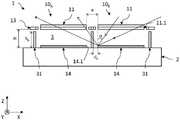
图1示出了这种检测装置1的热检测器10的示例。敏感像素的每个吸收膜11以与衬底2的非零距离悬置在所述衬底上方。为了改善待检测的电磁辐射的吸收,可以在面对吸收膜11的衬底2上放置反射层14。然后选择吸收膜11和反射层14之间的间隔以形成具有包括在待检测电磁辐射的波长范围内的参考波长的谐振的四分之一波长的腔。FIG. 1 shows an example of a
但是,需要布置减少了串扰的这种检测装置。However, it is necessary to arrange such a detection device that reduces crosstalk.
发明内容SUMMARY OF THE INVENTION
本发明旨在至少部分地弥补现有技术的缺点,并且更具体地提出一种具有减小的串扰的电磁(例如,红外)辐射检测装置。The present invention aims to at least partially remedy the disadvantages of the prior art, and more particularly proposes an electromagnetic (eg infrared) radiation detection device with reduced crosstalk.
为此,本发明的目的是一种电磁辐射的检测装置,包括:To this end, the object of the present invention is a detection device for electromagnetic radiation, comprising:
-衬底,其包括读取电路;- a substrate comprising a reading circuit;
-热检测器的矩阵,其用于吸收待检测的电磁辐射,布置在所述衬底上,每个热检测器包括:- a matrix of thermal detectors for absorbing the electromagnetic radiation to be detected, arranged on said substrate, each thermal detector comprising:
o吸收膜,其通过设置在所述衬底上并与衬底接触的锚固柱并且通过保持臂而悬置在衬底上方,所述锚固柱和保持臂确保吸收膜与读取电路的电连接,以及o Absorber film suspended above the substrate by anchor posts disposed on and in contact with the substrate and by retaining arms that ensure electrical connection of the absorber film to the readout circuit ,as well as
o反射层,其设置在面对所述吸收膜的衬底上。o A reflective layer disposed on the substrate facing the absorber film.
根据本发明,检测装置包括至少一个不透明竖直壁,所述至少一个不透明竖直壁设置在衬底上并与该衬底接触,并且在相邻的两个热检测器之间纵向延伸,并且由对于待检测的电磁辐射不透明的材料制成。According to the invention, the detection device comprises at least one opaque vertical wall disposed on and in contact with the substrate and extending longitudinally between two adjacent thermal detectors, and Made of a material that is opaque to the electromagnetic radiation to be detected.
另外,不透明竖直壁沿穿过相邻的两个锚固柱的轴线纵向延伸。换言之,不透明竖直壁与穿过相邻的两个柱的轴线同轴地延伸。此外,每个锚固柱是这样的结构,其沿着与平行于衬底的平面正交的轴线的高度大于其在平行于衬底的平面中的尺寸。“设置在衬底上”是指沿着与平行于衬底的平面正交的轴线布置在衬底上。Additionally, an opaque vertical wall extends longitudinally along an axis passing through two adjacent anchor posts. In other words, the opaque vertical wall extends coaxially with the axis passing through the two adjacent columns. Furthermore, each anchor post is a structure whose height along an axis orthogonal to a plane parallel to the substrate is greater than its dimension in a plane parallel to the substrate. "Disposed on the substrate" means disposed on the substrate along an axis normal to a plane parallel to the substrate.
此外,不透明竖直壁与至少一个锚固柱一体地实现。每个不透明竖直壁有利地由与锚固柱相同的一种或更多种材料制成。Furthermore, the opaque vertical wall is realized integrally with the at least one anchoring post. Each opaque vertical wall is advantageously made of the same material or materials as the anchoring posts.
该检测装置的一些优选的但非限制性的方面如下。Some preferred but non-limiting aspects of the detection device are as follows.
每个热检测器在与衬底平行的平面中可以被不透明竖直壁包围。每个热检测器可以被连续或不连续地包围。Each thermal detector may be surrounded by an opaque vertical wall in a plane parallel to the substrate. Each thermal detector can be surrounded continuously or discontinuously.
每个热检测器可以包括四个锚固柱。在平行于衬底的平面中,每个锚固柱位于吸收膜的一侧被至少两个不透明竖直壁所围绕,所述至少两个不透明竖直壁沿其纵向轴线彼此分开。两个不透明竖直壁优选地以同轴的方式延伸。Each thermal detector may include four anchoring posts. In a plane parallel to the substrate, each anchoring post is surrounded on one side of the absorbent film by at least two opaque vertical walls separated from each other along its longitudinal axis. The two opaque vertical walls preferably extend in a coaxial manner.
不透明竖直壁可以与保持臂和吸收膜分开。这因此使得能够排出用于实现热检测器的牺牲层。另外,不透明竖直壁的存在不会破坏吸收膜的热绝缘。The opaque vertical wall can be separated from the retaining arm and the absorbing film. This thus enables the sacrificial layer for realizing the thermal detector to be ejected. Additionally, the presence of opaque vertical walls does not disrupt the thermal insulation of the absorber film.
该检测装置可以包括多个不透明竖直壁。至少两个不透明竖直壁可以在相邻的两个热检测器的吸收膜之间纵向延伸,所述不透明竖直壁沿其纵轴彼此分开。The detection device may comprise a plurality of opaque vertical walls. At least two opaque vertical walls may extend longitudinally between the absorbing films of two adjacent thermal detectors, the opaque vertical walls being separated from each other along their longitudinal axis.
所述不透明竖直壁可以沿着其纵向轴线彼此间隔开小于或等于λ0/10的距离,其中λ0为待检测的电磁辐射的波长范围的中央波长。The opaque vertical walls may be spaced apart from each other along their longitudinal axis by a distance less than or equal to λ0 /10, where λ0 is the central wavelength of the wavelength range of the electromagnetic radiation to be detected.
所述距离可以小于或等于1.4μm。The distance may be less than or equal to 1.4 μm.
同一热检测器被彼此分开且彼此间隔开非零距离的多个不透明竖直壁包围。The same thermal detector is surrounded by a plurality of opaque vertical walls separated from each other and at a non-zero distance from each other.
不透明材料可以具有小于或等于5%、优选小于或等于1%的待检测的电磁辐射的透射率。The opaque material may have a transmittance of less than or equal to 5%, preferably less than or equal to 1%, of the electromagnetic radiation to be detected.
待检测的电磁辐射的波长范围可以为8μm至14μm。The wavelength range of the electromagnetic radiation to be detected may be from 8 μm to 14 μm.
一个或更多个不透明竖直壁可以以热检测器的侧的长度的至少50%与该热检测器的同一侧连续地邻接。One or more opaque vertical walls may be continuously adjoining the same side of the thermal detector by at least 50% of the length of the side of the thermal detector.
本发明还涉及一种用于制造根据前述特征中的任一项所述的检测装置的方法。该方法包括以下步骤:The invention also relates to a method for manufacturing a detection device according to any of the preceding features. The method includes the following steps:
-提供衬底;- provide the substrate;
-在衬底上沉积牺牲层;- depositing a sacrificial layer on the substrate;
-穿过牺牲层实现至少一个不透明竖直壁和锚固柱;- realization of at least one opaque vertical wall and anchoring post through the sacrificial layer;
-在牺牲层上实现保持臂和吸收膜;- Realization of retaining arms and absorption film on sacrificial layers;
-去除牺牲层。-Remove the sacrificial layer.
有利地,锚固柱和不透明竖直壁同时并且使用相同的一种或更多种材料制成。Advantageously, the anchoring posts and the opaque vertical walls are made simultaneously and using the same material or materials.
有利地,不透明竖直壁沿与平行于衬底的平面正交的轴线的高度基本上等于锚固柱的高度。Advantageously, the height of the opaque vertical wall along an axis orthogonal to a plane parallel to the substrate is substantially equal to the height of the anchoring post.
附图说明Description of drawings
通过阅读以下通过以非限制性示例的形式给出并且参考附图做出的本发明的优选实施例的详细描述,本发明的其他方面、目的、优点和特征将变得更加显而易见,在这些附图中:Other aspects, objects, advantages and features of the present invention will become more apparent on reading the following detailed description of preferred embodiments of the invention, given by way of non-limiting example and with reference to the accompanying drawings, in which In the picture:
已被描述的图1是根据现有技术的示例的检测装置的热检测器的示意性立体图;FIG. 1 , which has been described, is a schematic perspective view of a thermal detector of a detection device according to an example of the prior art;
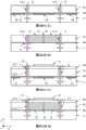
图2A和2B是根据一个实施例的检测装置的俯视示意图,其示出了敏感像素的悬置的吸收膜(图2A)和由不透明竖直壁隔开的反射层(图2B);2A and 2B are schematic top views of a detection device showing a suspended absorbing film (FIG. 2A) of a sensitive pixel and a reflective layer (FIG. 2B) separated by opaque vertical walls, according to one embodiment;
图3A和3B是图2A和2B所示的检测装置沿剖面A-A(图3A)和沿剖面B-B(图3B)的示意图;3A and 3B are schematic views of the detection device shown in FIGS. 2A and 2B along section A-A (FIG. 3A) and along section B-B (FIG. 3B);
图4A至4I是根据实施变型的检测装置的制造方法的不同阶段的示意性剖视图;4A to 4I are schematic cross-sectional views of different stages of a method of manufacturing a detection device according to implementation variants;
图5A至5C是根据实施变型的不同检测装置的俯视示意图,图5D是图5C所示的变型沿剖面E-E的示意图;5A to 5C are schematic top views of different detection devices according to implementation variants, and FIG. 5D is a schematic view of the variant shown in FIG. 5C along section E-E;
图6A是根据实施变型的检测装置的俯视示意图,并且图6B、6C、6D是图6A所示的变型沿不同剖面的示意性剖视图。Figure 6A is a schematic top view of a detection device according to an implementation variant, and Figures 6B, 6C, 6D are schematic cross-sectional views of the variant shown in Figure 6A along different sections.
具体实施方式Detailed ways
在附图和以下描述中,相同的附图标记表示相同或相似的元素。另外,为了附图的清晰性,不同的元素没有按比例显示。此外,不同的实施例和变型不是互相排斥的,并且可以彼此组合。除非另外指出,否则术语“基本上”、“大约”、“约”是指接近10%。此外,除非另外指出,否则表述“包括”应理解为“包括至少一个”。In the drawings and the following description, the same reference numbers refer to the same or similar elements. Additionally, for clarity of the drawings, various elements are not shown to scale. Furthermore, the different embodiments and variants are not mutually exclusive and can be combined with each other. The terms "substantially", "about", "about" mean approximately 10% unless otherwise indicated. Furthermore, the expression "comprising" should be understood to mean "including at least one" unless stated otherwise.
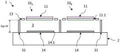
图2A-2B和3A-3B示出了根据一个实施例的电磁辐射的检测装置1。图2A和图2B是示出热检测器10的悬置的吸收膜11(图2A)和由不透明竖直壁31成对隔开的反射层14(图2B)的俯视图。图3A和3B是检测装置1沿剖面A-A(图3A)和沿剖面B-B(图3B)的截面图。Figures 2A-2B and 3A-3B illustrate a
在此,并在本说明书的其余部分中,定义了直接的三维直角坐标(X,Y,Z),其中平面(X,Y)是基本上平行于检测装置1的衬底2的平面,Z轴沿基本上与衬底2的平面正交的方向定向。术语“垂直”和“垂直地”在延伸时与基本上平行于Z轴的定向有关,术语“水平”和“水平地”与基本上平行于平面(X,Y)的定向有关。此外,术语“下部”和“上部”在延伸时与当沿+Z方向远离衬底2时增加的位置有关。Here, and in the remainder of this specification, direct three-dimensional Cartesian coordinates (X, Y, Z) are defined, where plane (X, Y) is the plane substantially parallel to the
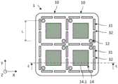
在该示例中,电磁辐射的检测装置1适于检测红外辐射。该检测装置包括形成敏感像素的热检测器10的矩阵,这里以2×2矩阵布置。仅通过说明的方式给出了该示例,可以实现更复杂的矩阵,例如高达1024×768的敏感像素10。In this example, the
该检测装置包括例如由硅基制成的衬底2,该衬底包括由CMOS技术实现的读取电路,使得可以施加热检测器10的操作所必需的电极化,并响应于目标电磁辐射的检测来读取来自热检测器的信号。The detection device comprises a
读取电路可以包括下部分(未示出),该下部分由适于实现读取电路的各种电子功能的MOS类型的电子器件(例如,晶体管、二极管、电容器)形成。该读取电路还包括多个电互连级,以确保各种MOS器件和热检测器10之间的电连接,以及读取电路的至少一个电连接垫(未示出)与检测装置1外部的电连接。The readout circuit may include a lower portion (not shown) formed of MOS type electronic devices (eg transistors, diodes, capacitors) suitable for implementing the various electronic functions of the readout circuit. The readout circuit also includes a number of electrical interconnect levels to ensure electrical connections between the various MOS devices and the
因此,读取电路包括多个电互连级,每个电互连级均由多条基本上平面的金属线形成,该多条基本上平面的金属线通过导电通孔22或垂直连接而连接至较低级的金属线。不同的电互连级通过称为金属间电介质(或IMD,英文为Inter-Metal Dielectric)的电介质层24彼此分开,这些金属间电介质层通过导电通孔22垂直地交叉。每个金属间电介质层24可以由氧化硅SiOx或氮化硅SiNx制成,或者甚至由基于具有低的相对介电常数的氧化硅的合金实现,例如SiOF、SiOC、SiOCH等。Thus, the readout circuit includes a plurality of electrical interconnect levels, each electrical interconnect level being formed by a plurality of substantially planar metal lines connected by
在该示例中,读取电路包括由金属线的第一部分21形成的较高的金属互连级,该第一部分与热检测器10相对,并且旨在与该检测器10电连接。该金属互连级的金属线部分21通过导电通孔22电连接到较低级的金属线部分23。这些部分和导电通孔通过金属间电介质层24彼此电隔离。In this example, the readout circuit comprises a higher level of metal interconnection formed by a
衬底2还可以包括蚀刻停止层(未示出),该蚀刻停止层覆盖由金属线的部分21和金属间电介质层24形成的表面。在适当的情况下,该蚀刻停止层特别适用于确保衬底2和读取电路针对例如在实现检测装置1时所实施用于蚀刻所使用的牺牲层的部分的例如在HF(氢氟酸)酸介质中的化学腐蚀的保护。因此,该蚀刻停止层形成气密且化学惰性的层,从而确保金属间电介质层和下层的金属线针对化学腐蚀的保护,并且该蚀刻停止层是电绝缘的,以避免金属线的部分之间发生任何电短路。蚀刻停止层可以由氧化铝Al2O3、或者甚至由氮化铝或氟化物制成。该蚀刻停止层的厚度可以为几十到几百纳米,例如为10nm到500nm。The
热检测器10中的每个包括适于吸收待检测的辐射的部分。该吸收部分与衬底2热绝缘,并设置在称为吸收膜的膜11处,该吸收膜通过保持和绝热元件(例如与该保持和绝热臂13相关的锚固柱12)悬置在衬底2上方。Each of the
锚固柱12是导电的并且局部地穿过蚀刻停止层以确保与金属线的部分21电接触。当热检测器10被设计用于检测波长为8μm到14μm的红外辐射(大气传输的LWIR带)时,吸收膜11与衬底2、更具体地与反射层14间隔开通常为1μm到5μm的距离H,例如大约2μm,因此形成四分之一波长腔3,从而改善悬浮膜11对电磁辐射的吸收。锚固柱12可以具有杆或柱的形状,其在XY平面中的横截面为大致为圆形轮廓(例如圆形)、甚至多边形(例如正方形或矩形),其面积为例如0.05μm2到5μm2,例如等于0.2μm2。所述锚固柱可以基于铜或钨实现,例如由Cu、W或Wsi制成,并且必要时包括基于钛的阻挡层。The anchoring posts 12 are conductive and pass locally through the etch stop layer to ensure electrical contact with the
每个敏感像素10还包括位于衬底2上的反射层14,在该示例中,该反射层位于蚀刻停止层上。如下所述,该反射层可以变型地位于蚀刻停止层下方,并且可以由较高的互连级的金属线的一部分形成。反射层14可以由至少一种金属材料制成,例如由基于铜、铝或甚至钨的至少一种材料制成。在所述反射层位于蚀刻停止层下方的情况下,该反射层可以由在每个敏感像素下方延伸的相同连续层形成。那么每个反射层14是同一连续的反射层的区域。Each
在下面的描述中,热检测器10是辐射热计,其吸收膜11包括热敏电阻材料,该热敏电阻材料的热导率随吸收膜11的加热而变化。然而,该示例仅以说明性的方式给出并且绝非限制性的。可以使用任何其他类型的热检测器10,例如热电、铁电、甚至热电堆检测器。In the following description, the
特别地通过将不同的热检测器10的保持臂13连接到同一锚固柱12,可以使热检测器10彼此靠近,然后适配热检测器的读取架构,如在文档EP1106980和EP1359400中对其进行描述地。这通过保持臂13的伸长而提高了检测器的灵敏度,并且通过减小非专用于吸收电磁辐射的每个敏感像素10的面积而提高了填充率。因此,检测装置1特别适用于小的模压步长,特别是小于或等于12μm的步长。In particular by connecting the holding
检测装置1包括至少一个不透明竖直壁31,所述至少一个不透明竖直壁位于相邻的两个敏感像素10之间,并且由对于待检测的电磁辐射不透明的材料制成,也就是说该材料的透射率小于或等于5%,甚至小于或等于1%。所述至少一个不透明竖直壁被配置为限制相邻的两个敏感像素10之间的串扰。串扰(英文为crosstalk)或光学串扰是敏感像素10对其相邻像素的影响的现象。特别地,涉及由敏感像素10A检测入射在相邻的敏感像素10B上的电磁辐射的一部分已经被反射层14反射的情况。串扰导致检测到的图像的对比度降低,并因此降低检测装置1的调制传递函数(FTM)。The
因此,在该示例中,不透明竖直壁31设置在相邻的两个敏感像素10之间,并且更准确地位于敏感像素10A的吸收膜11与相邻的敏感像素10B的吸收膜之间。述不透明竖直壁在纵向上基本上平行于吸收膜11的边缘11.1延伸。所述不透明竖直壁可以是直线的,如图2B所示,甚至可以是弯曲的,或者可以由多个直线部分形成,并两两倾斜。所述不透明竖直壁从衬底2沿着Z轴并且基本上垂直于衬底竖直地延伸。Therefore, in this example, the opaque
通常,如下所述,不透明竖直壁31可以与锚固柱12(见图2B)一体地实现或与锚固柱不同,也就是说,该不透明竖直壁没有物理连接到锚固柱(见图5B和5C)。优选地,每个不透明竖直壁31与保持臂13和不同的敏感像素10的吸收膜11分离,这避免了对热检测器10的热和/或电特性的任何干扰。在这种情况下,一方面不透明竖直壁31与另一方面的保持臂13和吸收膜11之间的间隔可以是垂直间隔(沿Z轴)和/或水平间隔(在XY平面内)。优选地,特别是当不透明竖直壁31与锚固柱12一体地实现时,所述不透明竖直壁也与相邻的敏感像素10的反射层14分离,以在必要时避免通过反射层14使锚固柱12电短路。Typically, as described below, the opaque
每个不透明竖直壁31的长度大于其宽度,例如,其长/宽比大于或等于2,优选地大于或等于5,或甚至是10。说明性地,不透明竖直壁可以因此具有500nm及以下的宽度,和5μm及以上的长度。每个不透明竖直壁31的宽度可以约为几百纳米到几微米。所述宽度优选小于1μm,并且优选小于或等于500nm。The length of each opaque
优选地,位于相邻的两个敏感像素10之间的至少一个不透明竖直壁31的长度大于或等于敏感像素一侧的长度L的50%、75%,并且优选为90%。在此,将敏感像素一侧的长度L定义为将敏感像素的两个锚固柱12的中心分开的距离,其中,锚固柱12的中心的投影在与所涉及的敏感像素的吸收膜11的边缘11.1平行的轴线上正交。替代地,如图2B所示,多个不透明竖直壁31可以在与吸收膜11的同一边缘11.1相对的方向上纵向延伸,并且由此形成纵向的一组不透明竖直壁31。然后,该纵向的一组不透明竖直壁31的累积长度可以大于或等于敏感像素的一侧的长度L的50%、优选75%、甚至90%。Preferably, the length of at least one opaque
在多个不透明竖直壁31形成同一纵向组的情况下,不透明竖直壁31沿着纵向轴线有利地两两间隔小于或等于λ0/10、甚至λ0/20,λ0是待检测的电磁辐射的波长范围的中心波长,例如对于8μm到14μm的待检测的电磁辐射的波长范围,该中心波长大约等于10μm或11μm。距离因此可以小于或等于1.4μm,例如小于或等于1.2μm,例如等于约1μm,或甚至等于约500nm。因此,将同一纵向组的两个不透明竖直壁31分开的该竖直开口32使得能够限制串扰,只要光束“看到”相同的连续的不透明竖直壁,而不是彼此分离的两个不透明竖直壁即可。另外,该竖直开口使得能够避免锚固柱之间的电短路的任何风险,特别是当两个连续的不透明竖直壁电连接到不同的锚固柱时。此外,该竖直开口还使得能够加速对在制造吸收膜11(下文中详述)期间使用的牺牲材料的蚀刻,并使其更加有效地排出。In the case of a plurality of opaque
在该示例中,如图3A所示,竖直开口32沿Z轴的高度等于两个不透明竖直壁31的高度,使得这些不透明竖直壁31彼此分开。作为变型,两个连续的不透明竖直壁31可以不是分离的,并且因此可以通过纵向部分(未示出)彼此连接,使得竖直开口32的高度小于所述不透明竖直壁31的高度。在这种情况下,这些连续的不透明竖直壁31不电连接到单独的锚固柱,从而避免了敏感像素10的电短路。In this example, as shown in FIG. 3A , the height of the
如图3B所示,每个不透明竖直壁31可具有高度hp,该高度配置成特别限制由敏感像素10A的吸收膜11接收入射在相邻的敏感像素10B上的电磁辐射的已被其反射层14反射的部分。该高度hp优选大于或等于dp/tan(α),其中dp是将敏感像素10的反射层14的边缘与不透明竖直壁31相对的边缘分开的平均距离,并且α是相对于法线的最小角度,该最小角度由敏感像素10B的反射层14反射的电磁辐射束形成并且由相邻的敏感像素10A的吸收膜11检测。在第一阶中,tan(α)=e/H,其中e是使敏感像素10的反射层14的边缘14.1相对于相邻的敏感像素10的吸收膜11相对的边缘分开的平均距离,H是沿Z轴使反射层14与吸收膜11分开的距离,即位于吸收膜下方的四分之一波长腔3的高度。每个或某些不透明竖直壁31可以具有高度hp,这也使得能够限制入射在相邻的敏感像素10B上的辐射的已被像素10B的吸收膜11沿敏感像素10A的反射层14的方向透射的部分。通常,不透明竖直壁31的高度hp有利地大于或等于四分之一波长腔3的高度H的90%,该四分之一波长腔等于锚固柱12的高度。As shown in FIG.3B , each opaque
每个不透明竖直壁31由对于待检测的电磁辐射不透明的的至少一种材料制成。对于具有例如为大约8μm到14μm的波长范围的辐射,不透明竖直壁31因此可以由铜、钨、铝等以及它们的合金实现。例如Ti、TiN或TiW的钛基或者例如Ta或TaN的钽基的壳体可以包围由基于Cu、W实现的芯的外围。该壳体可以确保阻挡层相对于铜或钨的可能扩散的功能。该壳体的厚度约为几十纳米,并且不改变不透明竖直壁31的光学特性。通常,“基于化学元素”是指材料由该化学元素形成,或者是由至少该化学元素形成的合金。优选地,不透明竖直壁31由对于待检测的电磁辐射的反射材料(例如铜、钨和铝等以及它们的合金)制成,从而使得能够改善检测装置的调制传递函数(FTM)的功能。Each opaque
优选地,每个敏感像素10由至少一个不透明竖直壁31限定边界,该不透明竖直壁在该敏感像素10与相邻的敏感像素10之间延伸。同样,该组不透明竖直壁31形成了蜂巢形状的光学隔离结构,每个蜂巢都是用于接收待检测的电磁辐射的热检测器10位于其中的腔。因此,该光隔离结构使得能够极大地限制敏感像素10之间的串扰。Preferably, each
因此,光隔离结构包括位于相邻的两个敏感像素10的吸收膜11之间的至少一个不透明的纵向部分,所述至少一个不透明的纵向部分沿着基本上与所述吸收膜11的边缘11.1平行的纵向轴线延伸。优选地,每个敏感像素10被四个不透明的纵向部分包围。每个不透明的纵向部分由从衬底2沿着基本平行于Z轴的竖直轴线延伸的至少一个不透明竖直壁31形成。每个不透明竖直壁31设置在相邻的两个敏感像素10之间,并因此在所述敏感像素10的吸收膜11之间。有利地,围绕同一敏感像素10的不透明竖直壁31彼此分开,从而加速了在制造四分之一波长腔3(下文所述)期间使用的牺牲材料的蚀刻并使得能够有效的排出,同时在必要时消除敏感像素的电短路的风险。所述不透明竖直壁优选彼此间隔小于或等于λ0/10、甚至λ0/20的距离,例如小于或等于1.4μm、甚至1μm或更小的距离。Thus, the optical isolation structure comprises at least one opaque longitudinal portion located between the
在图2B所示的示例中,光隔离结构的不透明竖直壁31沿着有利地穿过两个锚固柱12的轴线纵向延伸,从而使得能够最大化填充率(英文为fill factor),即在衬底2的平面中吸收膜11的面积与敏感像素10的总面积之比。In the example shown in FIG. 2B , the opaque
另外,不透明竖直壁31在此有利地与锚固柱12一体地实现,从而提高了不透明竖直壁31的机械强度。因此,不透明竖直壁31和锚固柱12优选地由相同的材料制成,这简化了制造检测装置1的方法的步骤。In addition, the opaque
不透明竖直壁31可以沿着Z轴位于保持臂13下方,也就是说垂直于保持臂13,甚至位于吸收膜11下方。如图3B所示,不透明竖直壁31的高度hp小于四分之一波长腔3的高度H,以避免与保持臂13和吸收膜11接触。因此,光隔离结构不会或几乎不会降低热检测器的热和/或电特性。举例来说,不透明竖直壁31可以与保持臂13和/或吸收膜11间隔大于或等于100nm、例如等于200nm的距离。该距离可以是四分之一波长腔3的高度H的大约10%。其他的不透明竖直壁31可以不与保持臂13或保持臂13垂直,并且具有大于或等于四分之一波长腔3的高度H的高度hp。因此,这样的壁31的高度可以等于锚固柱12的高度(例如参见如下所述的图5D)。The opaque
因此,根据本实施例的检测装置1通过在相邻的两个敏感像素10之间设置至少一个不透明竖直壁31而降低了串扰,特别是当每个敏感像素10通过有这样的不透明竖直壁31与其邻近敏感像素光学上分开时。包围同一敏感像素10的不透明竖直壁31彼此不同的事实使得能够提高蚀刻反应的速度并使得在吸收膜11的制造期间使用的牺牲材料更有效地排出。此外,不透明竖直壁31沿着穿过锚固柱12的轴线纵向地定位的事实使得能够增大填充率(fill factor)。Therefore, the
因此,根据本发明的检测装置1与专利申请EP2447688中描述的检测装置不同,该专利申请的检测装置包括参考热检测器,该参考热检测器通过吸收罩与其环境完全光隔离。该热检测器具有与敏感像素相同的吸收结构,但是由于该热检测器不用于接收待检测的电磁辐射,因此不能被认为是敏感像素。而且,根据现有技术的该文档的该检测装置没有设置被配置为减小相邻的敏感像素10之间的串扰的装置。Thus, the
根据本发明的检测装置1也与专利申请EP3067674中描述的检测装置不同,该专利申请的检测装置包括在相邻的两个敏感像素10之间设置的竖直壁。实际上,这些竖直壁是封装盖的部分,该封装盖根据定义以对待检测的电磁辐射透明的材料制成。根据现有技术的该文档的该检测装置没有设置被配置为减小相邻的敏感像素10之间的串扰的结构装置。The
图4A至4I示出了根据一个实施例的用于制造检测装置1的方法的不同步骤,其与图2A至2B和图3A至3B所示的不同之处主要在于反射层14由读取电路的上级的金属线的部分形成。Figures 4A to 4I show different steps of a method for manufacturing the
参照图4A,提供了衬底2,其包括能够提供并测量由热检测器传递的信号的CMOS电路类型的读取电路。因此,所述衬底包括通过金属互连电连接到热检测器的有源电子元件(例如二极管、晶体管、电容器、电阻器等),以及用于将检测装置1电连接到外部电子器件的一个或更多个连接柱(未示出)。如上所述,这里的读取电路包括电互连级,该电互连级包括通过导电通孔22电连接至较低电互连级的金属线的部分23的金属线的第一部分21,和用于形成反射层的同一金属线的第二部分14。通孔和金属线通过金属间电介质层24彼此分开。衬底2在此包括上表面,在该上表面处同一金属线的部分21、14与金属间电介质层24齐平。实现衬底2的该步骤可以与文件EP2743659中描述的步骤相同或相似。Referring to Figure 4A, a
将蚀刻停止层40沉积在衬底2的上表面的至少一部分上。因此,该蚀刻停止层连续地覆盖金属间电介质层24、金属线的第一部分21和反射层14。蚀刻停止层40包括对化学蚀刻基本上呈惰性的材料,该化学蚀刻随后被实施以去除矿物牺牲层,更确切地说,在气相的HF介质中的化学侵蚀。因此,蚀刻停止层40使得能够防止在去除牺牲层的步骤期间CMOS电路的金属间电介质层被蚀刻。所述蚀刻停止层可以由氧化铝Al2O3、甚至氮化铝、三氟化铝或无意掺杂的非晶硅形成。所述蚀刻停止层可以例如通过ALD(英语为Atomic LayerDeposition)沉积,并且具有例如大约十纳米到几百纳米的厚度,例如20nm到150nm的厚度。An
参照图4B和4C(图4B是沿着图4C的剖面CC的视图),通过PECVD(英语为PlasmaEnhanced Chemical Vapor Deposition)将由优选矿物材料(例如由沉积的氧化硅)实现的牺牲层41沉积在衬底2上。该牺牲层基本上在衬底2的整个表面上连续地延伸并覆盖蚀刻停止层40。在该示例中,不透明竖直壁31用于位于保持臂13下方和/或吸收膜11下方,牺牲层41沿Z轴的厚度在此限定将随后实现的不透明竖直壁31的高度hp。Referring to FIGS. 4B and 4C (FIG. 4B is a view along section CC of FIG. 4C), a
然后实现用于形成锚固柱12的竖直孔42,以及用于形成不透明竖直壁31的沟槽43。竖直孔42和沟槽43有利地同时形成,也就是说同时进行。所述竖直孔和沟槽是通过光刻和蚀刻实现的。竖直孔42穿过牺牲层41以及蚀刻停止层40以分别通向金属线的第一部分21。竖直孔42可以在平面(X,Y)上具有圆形的横截面,例如圆形、甚至多边形,并且面积在这里基本上等于0.2μm2。沟槽43穿过牺牲层41,直到在这里通向蚀刻停止层40。沟槽43在平面(X,Y)中纵向延伸,从而位于相邻的两个敏感像素10之间。在此,所述沟槽在平面(X,Y)中的宽度基本上等于0.5μm,或更小。在该示例中,沟槽43在纵向上通向竖直孔42,这是因为不透明竖直壁31在这里将与锚固柱12一体地实现。The
参照图4D和4E(图4D是沿着剖面C-C的视图,图4E是沿着剖面D-D的视图),然后在竖直孔42中实现锚固柱12的下部12.1,并且在沟槽43中实现不透明竖直壁31。锚固柱12的下部12.1和不透明竖直壁31在此可以同时产生。它们也被一体地实现,也就是说,每个不透明竖直壁31以与锚固柱12一起的方式具有连续性。它们是通过由一种或更多种导电且光学不透明的材料填充竖直孔42和沟槽43而实现的。举例来说,它们可以包括通过MOCVD(英语为Metal Organic Chemical Vapor Deposition)沉积在竖直孔42和沟槽43的侧面上的基于钛的阻挡层,以及例如通过ECD(英语为Electrochemical Deposition)沉积的基于铜或钨、甚至基于铝的芯部,填充了由粘结层横向界定的空间。因此,不透明竖直壁31可以以与锚固柱12的下部12.1的形成同时的方式并且在材料方面以相同的方式实现。CMP步骤然后使得能够平坦化由牺牲层41、锚固柱12的下部12.1和不透明竖直壁31形成的上表面。Referring to Figures 4D and 4E (Figure 4D is a view along section C-C, Figure 4E is a view along section D-D), the lower part 12.1 of the anchoring
参照图4F和4G(图4F是沿着剖面C-C的视图,图4G是沿着剖面D-D的视图),然后实现锚固柱12的上部12.2。为此,在第一牺牲层41上沉积第二牺牲层44,并通过第二牺牲层44的厚度形成竖直孔,以通向锚固柱12的下部12.1。然后以与实现下部12.1的步骤相同或相似的方式来实现锚固柱12的上部12.2。由此获得锚固柱12,其高度对应于四分之一波长腔3的期望高度H。这里,锚固柱的高度H大于不透明竖直壁31的高度hp,从而使得能够在没有与不透明竖直壁31热/电接触的风险的情况下实现吸收膜11。作为变型,锚固柱12的上部12.2可以通过沉积例如基于TiN和TiN实现的连续金属层来制造,然后,蚀刻连续金属层,以便仅将金属柱保持在下部12.1上方,从而形成上部12.2。锚固柱12的上部12.2可以具有大约1到几百纳米的厚度,例如大约100到200nm的厚度。Referring to Figures 4F and 4G (Figure 4F is a view along section CC and Figure 4G is a view along section DD), then the upper part 12.2 of the anchoring
然后实现保持臂13和吸收膜11。该步骤可以以与文档EP2743659中描述的相同或相似的方式进行,因此不再赘述。因此,吸收膜11可以包括第一材料和第二热敏电阻材料,所述第一材料适于吸收目标电磁辐射,所述第二热敏电阻材料的电导率根据膜的加热而变化。The holding
参照图4H和4I(图4H是沿着剖面C-C的视图,图4I是沿着剖面D-D的视图),执行牺牲层41、44的蚀刻,以使吸收膜11悬置。蚀刻可以通过在气相中用氢氟酸(HF)进行化学侵蚀来进行。化学侵蚀基本上蚀刻了位于热检测器10处的所有牺牲层41、44,因此使得能够将吸收膜11悬置在衬底2上方。化学侵蚀反应因此更快并且化学侵蚀反应的产物穿过使不透明竖直壁31彼此分离的竖直开口32可以有效地排出,使得在四分之一波长腔3中几乎不再存在牺牲材料的残留物。另外,使不透明竖直壁31分离的竖直开口32的小尺寸也使得能够限制电磁辐射从敏感像素10到另一个的透射,从而减小串扰。4H and 4I (FIG. 4H is a view along the section C-C, and FIG. 4I is a view along the section D-D), etching of the
图5A至5C是根据不同实施变型的检测装置的俯视图,其基本上通过不透明竖直壁31的布置以及锚固柱12的数量和布置而与图2A-2B和3A-3B所示的检测装置不同。图5D是沿图5C所示的变型的平面E-E的剖视图。FIGS. 5A to 5C are top views of detection devices according to different implementation variants, which differ substantially from the detection devices shown in FIGS. 2A-2B and 3A-3B by the arrangement of the opaque
因此,图5A示出了检测装置1,其中每个敏感像素10包括不与相邻敏感像素10共享的两个锚固柱12。在该示例中,不透明竖直壁31与锚固柱12一体地实现,而其他的则是分开的。此外,不透明竖直壁31的两个平行的行布置在相邻的两个敏感像素10之间。通常,当不透明竖直壁31由反射材料实现时,包围每个敏感像素10的吸收膜12的不透明竖直壁的这种布置是特别有利的,由此改善了检测装置1的调制传递函数。Thus, FIG. 5A shows a
图5B示出了检测装置1,其中不透明竖直壁31中的每个与锚固柱12分开。因此,在每个不透明竖直壁31与相邻的锚固柱12之间形成竖直开口32,该竖直开口在XY平面中的尺寸优选小于或等于λ0/10、甚至λ0/2,例如小于或等于1.4μm。反射层14的每一侧在此由单个不透明竖直壁31界定。此外,单个不透明竖直壁31位于相邻的两个反射层14之间,从而使得能够提高与每个敏感像素10相关的填充率。不与保持臂13或吸收膜11垂直的不透明竖直壁31可以具有更大的高度hp,例如可以具有与锚固柱12相同的高度,进一步减少敏感像素10之间的串扰。FIG. 5B shows the
图5C和5D示出了检测装置1,其与图5A所示的检测装置的主要区别在于,不透明竖直壁31没有沿着穿过相邻的两个锚固柱12的轴线纵向地设置,而是不仅包围敏感像素10的吸收膜11,而且还包围锚固柱12。与每个敏感像素10相关的填充率不是最佳的,但是不透明竖直壁31在此处形成位于敏感像素10的角处以及位于反射层14的边界14.1中间的多个竖直开口32,因此使得能够更快地蚀刻一个或更多个牺牲层以及更大程度地排出牺牲材料。此外,不透明竖直壁31在此不位于保持臂13下方或吸收性膜11下方,使得所述不透明竖直壁的高度hp可以等于、甚至大于四分之一波长腔3的高度H。例如,所述不透明竖直壁的高度hp可以基本上等于锚固柱12的高度。因此,进一步减小了敏感像素10之间的串扰。与参照图4A至4I描述的变型相比,这种变型的实现被简化,这是因为不需要实现锚固柱12的上部12.2。Figures 5C and 5D show the
刚刚已经描述了具体实施例。不同的变型和修改对本领域技术人员将是显而易见的。Specific embodiments have just been described. Various variations and modifications will be apparent to those skilled in the art.
因此,图6A是根据另一实施变型的检测装置1的示意性局部视图。图6B、6C、6D分别是该检测装置1沿剖面A-A、B-B和C-C的剖视图。该检测装置与上述的检测装置的主要区别在于,不透明竖直壁31沿轴线Z的高度基本上等于锚固柱12的高度。不透明竖直壁在XY平面中沿热检测器10的四侧围绕该热检测器。每侧都由纵向上同轴延伸并在XY平面中由开口32间隔开的两个不透明竖直壁邻接。不透明竖直壁在XY平面中的厚度(或宽度)例如为200nm到500nm,并在XY平面中通过开口32彼此间隔开例如200nm到1μm的距离。每个不透明竖直壁与锚固柱12一体地实现并且由相同的一种或更多种材料实现。每个保持臂13在XY平面中从锚固柱12延伸。在此,在组装到吸收膜11之前,每个保持臂与吸收膜11的两侧邻接。每个保持臂13可以在XY平面上具有例如为100nm到300nm的宽度。只要不透明竖直壁31的高度等于锚固柱12的高度,则保持臂13在XY平面上与所述锚固柱间隔例如为100nm到300nm的距离。因此,检测装置1在这里具有减小的串扰和高的填充系数。此外,壁31的机械强度由于它们与柱12一体地实现而增强。并且由于壁31和柱12用同一步骤实现并且由相同的一种或更多种材料制成的这一事实而简化了所述方法。Thus, FIG. 6A is a schematic partial view of a
Claims (13)
Translated fromChineseApplications Claiming Priority (3)
| Application Number | Priority Date | Filing Date | Title |
|---|---|---|---|
| FR1760961AFR3073941B1 (en) | 2017-11-21 | 2017-11-21 | REDUCED-DIAPHOTIE ELECTROMAGNETIC RADIATION DETECTION DEVICE |
| FR1760961 | 2017-11-21 | ||
| PCT/FR2018/052903WO2019102121A1 (en) | 2017-11-21 | 2018-11-19 | Device for detecting electromagnetic radiation with reduced crosstalk |
Publications (2)
| Publication Number | Publication Date |
|---|---|
| CN111373231Atrue CN111373231A (en) | 2020-07-03 |
| CN111373231B CN111373231B (en) | 2023-04-25 |
Family
ID=61521616
Family Applications (1)
| Application Number | Title | Priority Date | Filing Date |
|---|---|---|---|
| CN201880074533.0AActiveCN111373231B (en) | 2017-11-21 | 2018-11-19 | Electromagnetic radiation detection device with reduced crosstalk |
Country Status (5)
| Country | Link |
|---|---|
| US (1) | US11085828B2 (en) |
| EP (1) | EP3714243B1 (en) |
| CN (1) | CN111373231B (en) |
| FR (1) | FR3073941B1 (en) |
| WO (1) | WO2019102121A1 (en) |
Families Citing this family (2)
| Publication number | Priority date | Publication date | Assignee | Title |
|---|---|---|---|---|
| CN113720466B (en)* | 2021-03-26 | 2022-10-11 | 北京北方高业科技有限公司 | Infrared detector based on CMOS (complementary Metal oxide semiconductor) process |
| FR3125877B1 (en)* | 2021-07-30 | 2023-06-30 | Lynred | METHOD FOR MAKING A BLIND INFRARED IMAGING MICRO-BOLOMETER AND ASSOCIATED MICRO-BOLOMETER |
Citations (8)
| Publication number | Priority date | Publication date | Assignee | Title |
|---|---|---|---|---|
| US20030173504A1 (en)* | 2002-03-18 | 2003-09-18 | Honeywell International Inc. | Spectrally tunable detector |
| CN1760651A (en)* | 2005-09-06 | 2006-04-19 | 中国科学技术大学 | Optical display infra-red sensor |
| CN102124311A (en)* | 2008-10-07 | 2011-07-13 | Ulis股份公司 | Electromagnetic radiation detector with micropackage and device for detecting electromagnetic radiation using such detector |
| FR2966595A1 (en)* | 2010-10-26 | 2012-04-27 | Commissariat Energie Atomique | DEVICE FOR DETECTING ELECTROMAGNETIC RADIATION. |
| EP3067674A2 (en)* | 2015-02-20 | 2016-09-14 | Commissariat à l'Énergie Atomique et aux Énergies Alternatives | Device for detecting radiation comprising an encapsulation structure with improved mechanical strength |
| CN107063470A (en)* | 2015-12-15 | 2017-08-18 | 优利斯公司 | Detection device of suspended bolometric membrane with high absorption efficiency and signal-to-noise ratio |
| CN107121203A (en)* | 2016-02-24 | 2017-09-01 | 原子能和替代能源委员会 | Device for detecting electromagnetic radiation comprising a raised electrical connection pad |
| US20170328778A1 (en)* | 2016-05-13 | 2017-11-16 | Mitsubishi Electric Corporation | Thermal infrared detector and manufacturing method for thermal infrared detector |
Family Cites Families (9)
| Publication number | Priority date | Publication date | Assignee | Title |
|---|---|---|---|---|
| US7145143B2 (en)* | 2002-03-18 | 2006-12-05 | Honeywell International Inc. | Tunable sensor |
| JP5308814B2 (en)* | 2005-05-17 | 2013-10-09 | ハイマン・ゼンゾル・ゲゼルシャフト・ミト・ベシュレンクテル・ハフツング | Thermopile infrared sensor array |
| TWI369483B (en)* | 2010-08-30 | 2012-08-01 | Unimems Mfg Co Ltd | Miniature infrared sensor and manufacturing method thereof |
| FR2966596B1 (en) | 2010-10-26 | 2012-12-07 | Commissariat Energie Atomique | DEVICE FOR DETECTING ELECTROMAGNETIC RADIATION. |
| FR2999805B1 (en) | 2012-12-17 | 2017-12-22 | Commissariat Energie Atomique | METHOD FOR PRODUCING AN INFRARED DETECTION DEVICE |
| US9733128B2 (en)* | 2014-06-18 | 2017-08-15 | Todos Technologies Ltd. | Sensor array with self-aligned optical cavities |
| US9696199B2 (en)* | 2015-02-13 | 2017-07-04 | Taiwan Biophotonic Corporation | Optical sensor |
| US10794768B2 (en)* | 2016-06-21 | 2020-10-06 | Heimann Sensor Gmbh | Thermopile infrared individual sensor for measuring temperature or detecting gas |
| JP7116591B2 (en)* | 2018-05-18 | 2022-08-10 | キヤノン株式会社 | Imaging device and its manufacturing method |
- 2017
- 2017-11-21FRFR1760961Apatent/FR3073941B1/ennot_activeExpired - Fee Related
- 2018
- 2018-11-19WOPCT/FR2018/052903patent/WO2019102121A1/ennot_activeCeased
- 2018-11-19USUS16/765,385patent/US11085828B2/ennot_activeExpired - Fee Related
- 2018-11-19CNCN201880074533.0Apatent/CN111373231B/enactiveActive
- 2018-11-19EPEP18821718.6Apatent/EP3714243B1/enactiveActive
Patent Citations (8)
| Publication number | Priority date | Publication date | Assignee | Title |
|---|---|---|---|---|
| US20030173504A1 (en)* | 2002-03-18 | 2003-09-18 | Honeywell International Inc. | Spectrally tunable detector |
| CN1760651A (en)* | 2005-09-06 | 2006-04-19 | 中国科学技术大学 | Optical display infra-red sensor |
| CN102124311A (en)* | 2008-10-07 | 2011-07-13 | Ulis股份公司 | Electromagnetic radiation detector with micropackage and device for detecting electromagnetic radiation using such detector |
| FR2966595A1 (en)* | 2010-10-26 | 2012-04-27 | Commissariat Energie Atomique | DEVICE FOR DETECTING ELECTROMAGNETIC RADIATION. |
| EP3067674A2 (en)* | 2015-02-20 | 2016-09-14 | Commissariat à l'Énergie Atomique et aux Énergies Alternatives | Device for detecting radiation comprising an encapsulation structure with improved mechanical strength |
| CN107063470A (en)* | 2015-12-15 | 2017-08-18 | 优利斯公司 | Detection device of suspended bolometric membrane with high absorption efficiency and signal-to-noise ratio |
| CN107121203A (en)* | 2016-02-24 | 2017-09-01 | 原子能和替代能源委员会 | Device for detecting electromagnetic radiation comprising a raised electrical connection pad |
| US20170328778A1 (en)* | 2016-05-13 | 2017-11-16 | Mitsubishi Electric Corporation | Thermal infrared detector and manufacturing method for thermal infrared detector |
Also Published As
| Publication number | Publication date |
|---|---|
| WO2019102121A1 (en) | 2019-05-31 |
| US11085828B2 (en) | 2021-08-10 |
| US20200340864A1 (en) | 2020-10-29 |
| EP3714243A1 (en) | 2020-09-30 |
| FR3073941A1 (en) | 2019-05-24 |
| EP3714243B1 (en) | 2021-10-20 |
| FR3073941B1 (en) | 2021-01-15 |
| CN111373231B (en) | 2023-04-25 |
Similar Documents
| Publication | Publication Date | Title |
|---|---|---|
| JP6362323B2 (en) | Method for making an infrared detection device | |
| KR102419468B1 (en) | Method for making a device for detecting electromagnetic radiation comprising a layer of getter material | |
| KR102694853B1 (en) | Deivce for detecting electromagnetic radiation comprising a raised electrical connection pad | |
| US8026177B2 (en) | Silicon dioxide cantilever support and method for silicon etched structures | |
| CN108982973B (en) | Electromagnetic radiation detector encapsulated by thin layer transfer | |
| EP3024028A1 (en) | Uncooled infrared detector and methods for manufacturing the same | |
| KR102636590B1 (en) | Method For Producing A Bolometric Detector | |
| KR20190049577A (en) | Semiconductor image sensor | |
| TWI872159B (en) | Process for fabricating a device for detecting electromagnetic radiation | |
| US7754517B2 (en) | Method for manufacturing infrared detecting device | |
| CN111373231B (en) | Electromagnetic radiation detection device with reduced crosstalk | |
| US10981782B2 (en) | Process for fabricating a device for detecting electromagnetic radiation having an improved encapsulation structure | |
| US20210347636A1 (en) | Process for manufacturing a device for detecting electromagnetic radiation, comprising a suspended detection element | |
| JP2016194508A (en) | Radiation detection apparatus having an encapsulating structure with improved mechanical strength | |
| US20230213389A1 (en) | Method for manufacturing a detection device comprising a peripheral wall made of a mineral material | |
| JP2006297502A (en) | Semiconductor device and manufacturing method thereof | |
| RU2793118C2 (en) | Method for manufacturing a device with an improved encapsulating structure for detecting electromagnetic radiation |
Legal Events
| Date | Code | Title | Description |
|---|---|---|---|
| PB01 | Publication | ||
| PB01 | Publication | ||
| SE01 | Entry into force of request for substantive examination | ||
| SE01 | Entry into force of request for substantive examination | ||
| GR01 | Patent grant | ||
| GR01 | Patent grant |