CN111370386A - Fan-out system-in-package structure and method of making the same - Google Patents
Fan-out system-in-package structure and method of making the sameDownload PDFInfo
- Publication number
- CN111370386A CN111370386ACN202010285803.1ACN202010285803ACN111370386ACN 111370386 ACN111370386 ACN 111370386ACN 202010285803 ACN202010285803 ACN 202010285803ACN 111370386 ACN111370386 ACN 111370386A
- Authority
- CN
- China
- Prior art keywords
- layer
- metal
- wiring layer
- package structure
- fan
- Prior art date
- Legal status (The legal status is an assumption and is not a legal conclusion. Google has not performed a legal analysis and makes no representation as to the accuracy of the status listed.)
- Pending
Links
Images


Classifications
- H—ELECTRICITY
- H01—ELECTRIC ELEMENTS
- H01L—SEMICONDUCTOR DEVICES NOT COVERED BY CLASS H10
- H01L23/00—Details of semiconductor or other solid state devices
- H01L23/48—Arrangements for conducting electric current to or from the solid state body in operation, e.g. leads, terminal arrangements ; Selection of materials therefor
- H01L23/488—Arrangements for conducting electric current to or from the solid state body in operation, e.g. leads, terminal arrangements ; Selection of materials therefor consisting of soldered or bonded constructions
- H01L23/498—Leads, i.e. metallisations or lead-frames on insulating substrates, e.g. chip carriers
- H01L23/49811—Additional leads joined to the metallisation on the insulating substrate, e.g. pins, bumps, wires, flat leads
- H01L23/49816—Spherical bumps on the substrate for external connection, e.g. ball grid arrays [BGA]
- H—ELECTRICITY
- H01—ELECTRIC ELEMENTS
- H01L—SEMICONDUCTOR DEVICES NOT COVERED BY CLASS H10
- H01L21/00—Processes or apparatus adapted for the manufacture or treatment of semiconductor or solid state devices or of parts thereof
- H01L21/02—Manufacture or treatment of semiconductor devices or of parts thereof
- H01L21/04—Manufacture or treatment of semiconductor devices or of parts thereof the devices having potential barriers, e.g. a PN junction, depletion layer or carrier concentration layer
- H01L21/48—Manufacture or treatment of parts, e.g. containers, prior to assembly of the devices, using processes not provided for in a single one of the groups H01L21/18 - H01L21/326 or H10D48/04 - H10D48/07
- H01L21/4814—Conductive parts
- H01L21/4846—Leads on or in insulating or insulated substrates, e.g. metallisation
- H01L21/4853—Connection or disconnection of other leads to or from a metallisation, e.g. pins, wires, bumps
- H—ELECTRICITY
- H01—ELECTRIC ELEMENTS
- H01L—SEMICONDUCTOR DEVICES NOT COVERED BY CLASS H10
- H01L21/00—Processes or apparatus adapted for the manufacture or treatment of semiconductor or solid state devices or of parts thereof
- H01L21/70—Manufacture or treatment of devices consisting of a plurality of solid state components formed in or on a common substrate or of parts thereof; Manufacture of integrated circuit devices or of parts thereof
- H01L21/71—Manufacture of specific parts of devices defined in group H01L21/70
- H01L21/768—Applying interconnections to be used for carrying current between separate components within a device comprising conductors and dielectrics
- H01L21/76838—Applying interconnections to be used for carrying current between separate components within a device comprising conductors and dielectrics characterised by the formation and the after-treatment of the conductors
- H01L21/76895—Local interconnects; Local pads, as exemplified by patent document EP0896365
- H—ELECTRICITY
- H01—ELECTRIC ELEMENTS
- H01L—SEMICONDUCTOR DEVICES NOT COVERED BY CLASS H10
- H01L23/00—Details of semiconductor or other solid state devices
- H01L23/48—Arrangements for conducting electric current to or from the solid state body in operation, e.g. leads, terminal arrangements ; Selection of materials therefor
- H01L23/488—Arrangements for conducting electric current to or from the solid state body in operation, e.g. leads, terminal arrangements ; Selection of materials therefor consisting of soldered or bonded constructions
- H01L23/498—Leads, i.e. metallisations or lead-frames on insulating substrates, e.g. chip carriers
- H01L23/49811—Additional leads joined to the metallisation on the insulating substrate, e.g. pins, bumps, wires, flat leads
- H—ELECTRICITY
- H01—ELECTRIC ELEMENTS
- H01L—SEMICONDUCTOR DEVICES NOT COVERED BY CLASS H10
- H01L23/00—Details of semiconductor or other solid state devices
- H01L23/48—Arrangements for conducting electric current to or from the solid state body in operation, e.g. leads, terminal arrangements ; Selection of materials therefor
- H01L23/488—Arrangements for conducting electric current to or from the solid state body in operation, e.g. leads, terminal arrangements ; Selection of materials therefor consisting of soldered or bonded constructions
- H01L23/498—Leads, i.e. metallisations or lead-frames on insulating substrates, e.g. chip carriers
- H01L23/49838—Geometry or layout
- H—ELECTRICITY
- H01—ELECTRIC ELEMENTS
- H01L—SEMICONDUCTOR DEVICES NOT COVERED BY CLASS H10
- H01L23/00—Details of semiconductor or other solid state devices
- H01L23/52—Arrangements for conducting electric current within the device in operation from one component to another, i.e. interconnections, e.g. wires, lead frames
- H01L23/538—Arrangements for conducting electric current within the device in operation from one component to another, i.e. interconnections, e.g. wires, lead frames the interconnection structure between a plurality of semiconductor chips being formed on, or in, insulating substrates
- H01L23/5386—Geometry or layout of the interconnection structure
- H—ELECTRICITY
- H01—ELECTRIC ELEMENTS
- H01L—SEMICONDUCTOR DEVICES NOT COVERED BY CLASS H10
- H01L25/00—Assemblies consisting of a plurality of semiconductor or other solid state devices
- H01L25/16—Assemblies consisting of a plurality of semiconductor or other solid state devices the devices being of types provided for in two or more different subclasses of H10B, H10D, H10F, H10H, H10K or H10N, e.g. forming hybrid circuits
- H—ELECTRICITY
- H01—ELECTRIC ELEMENTS
- H01L—SEMICONDUCTOR DEVICES NOT COVERED BY CLASS H10
- H01L25/00—Assemblies consisting of a plurality of semiconductor or other solid state devices
- H01L25/18—Assemblies consisting of a plurality of semiconductor or other solid state devices the devices being of the types provided for in two or more different main groups of the same subclass of H10B, H10D, H10F, H10H, H10K or H10N
- H—ELECTRICITY
- H01—ELECTRIC ELEMENTS
- H01L—SEMICONDUCTOR DEVICES NOT COVERED BY CLASS H10
- H01L2224/00—Indexing scheme for arrangements for connecting or disconnecting semiconductor or solid-state bodies and methods related thereto as covered by H01L24/00
- H01L2224/01—Means for bonding being attached to, or being formed on, the surface to be connected, e.g. chip-to-package, die-attach, "first-level" interconnects; Manufacturing methods related thereto
- H01L2224/10—Bump connectors; Manufacturing methods related thereto
- H01L2224/15—Structure, shape, material or disposition of the bump connectors after the connecting process
- H01L2224/16—Structure, shape, material or disposition of the bump connectors after the connecting process of an individual bump connector
- H01L2224/161—Disposition
- H01L2224/16151—Disposition the bump connector connecting between a semiconductor or solid-state body and an item not being a semiconductor or solid-state body, e.g. chip-to-substrate, chip-to-passive
- H01L2224/16221—Disposition the bump connector connecting between a semiconductor or solid-state body and an item not being a semiconductor or solid-state body, e.g. chip-to-substrate, chip-to-passive the body and the item being stacked
- H01L2224/16225—Disposition the bump connector connecting between a semiconductor or solid-state body and an item not being a semiconductor or solid-state body, e.g. chip-to-substrate, chip-to-passive the body and the item being stacked the item being non-metallic, e.g. insulating substrate with or without metallisation
- H—ELECTRICITY
- H01—ELECTRIC ELEMENTS
- H01L—SEMICONDUCTOR DEVICES NOT COVERED BY CLASS H10
- H01L2224/00—Indexing scheme for arrangements for connecting or disconnecting semiconductor or solid-state bodies and methods related thereto as covered by H01L24/00
- H01L2224/01—Means for bonding being attached to, or being formed on, the surface to be connected, e.g. chip-to-package, die-attach, "first-level" interconnects; Manufacturing methods related thereto
- H01L2224/18—High density interconnect [HDI] connectors; Manufacturing methods related thereto
Landscapes
- Engineering & Computer Science (AREA)
- Physics & Mathematics (AREA)
- Microelectronics & Electronic Packaging (AREA)
- Condensed Matter Physics & Semiconductors (AREA)
- General Physics & Mathematics (AREA)
- Computer Hardware Design (AREA)
- Power Engineering (AREA)
- Manufacturing & Machinery (AREA)
- Ceramic Engineering (AREA)
- Geometry (AREA)
- Internal Circuitry In Semiconductor Integrated Circuit Devices (AREA)
- Production Of Multi-Layered Print Wiring Board (AREA)
Abstract
Translated fromChinese
Description
Translated fromChinese技术领域technical field
本发明属于半导体集成电路封装领域,特别是涉及一种扇出型系统级封装结构及其制作方法。The invention belongs to the field of semiconductor integrated circuit packaging, and in particular relates to a fan-out type system-level packaging structure and a manufacturing method thereof.
背景技术Background technique
随着5G通讯和人工智能(AI)时代的到来,应用于此类相关领域的芯片所要传输和高速交互处理的数据量非常巨大,该类芯片通常具有数量巨大的pad引脚(几百甚至上千个)、超精细的管脚大小和间距(几个微米甚至更小)。另一方面,移动互联网以及物联网方面的需求越来越强劲,电子终端产品的小型化和多功能化成为产业发展的大趋势。如何将多个不同种类的高密度芯片集成封装在一起构成一个功能强大且体积功耗又比较小的系统或者子系统,成为半导体芯片先进封装领域的一大挑战。With the advent of the era of 5G communication and artificial intelligence (AI), the amount of data to be transmitted and processed in high-speed interaction for chips used in such related fields is very large, and such chips usually have a huge number of pad pins (hundreds or even thousands), ultra-fine pin sizes and pitches (several microns or even smaller). On the other hand, the demand for mobile Internet and the Internet of Things is getting stronger and stronger, and the miniaturization and multi-functionalization of electronic terminal products have become the general trend of industrial development. How to integrate and package multiple different types of high-density chips together to form a system or subsystem with powerful functions and relatively low volume power consumption has become a major challenge in the field of advanced semiconductor chip packaging.
目前针对此类高密度芯片的多芯片集成封装,业界通常都是采用硅穿孔(TSV)、硅转接板(Si interposer)等方式进行,从而把芯片的超精细引脚进行引出和有效互联从而形成一个功能模块或者系统,但该技术的成本比较高,从而大大局限了它的应用范围。扇出型封装技术采用重构晶圆和重新布线RDL的方式为实现多芯片的集成封装提供了很好的平台,但是现有的扇出型封装技术中由于布线精度有限从而使得封装体的面积较大厚度较高,而且存在工序繁多、可靠性不高等诸多问题。At present, the multi-chip integrated packaging for such high-density chips is usually carried out in the industry by means of through-silicon (TSV), silicon interposer (Si interposer), etc., so as to lead out and effectively interconnect the ultra-fine pins of the chip. A functional module or system is formed, but the cost of this technology is relatively high, which greatly limits its application range. Fan-out packaging technology provides a good platform for realizing multi-chip integrated packaging by reconfiguring wafers and rewiring RDL. However, in the existing fan-out packaging technology, due to the limited wiring accuracy, the area of the package is limited. The larger thickness is higher, and there are many problems such as many processes and low reliability.
为适应微电子封装技术的多功能、小型化、便携式、高速度、低功耗和高可靠性发展趋势,系统级封装SIP(System In Package)技术作为新兴异质集成技术,成为越来越多芯片的封装形式,系统级封装是将多种功能芯片和元器件集成在一个封装内,从而实现一个完整的功能。系统级封装是一种新型封装技术,具有开发周期短,功能更多,功耗更低,性能更优良、成本价格更低,体积更小,质量轻等优点。In order to adapt to the development trend of multi-function, miniaturization, portable, high speed, low power consumption and high reliability of microelectronic packaging technology, system-in-package SIP (System In Package) technology, as an emerging heterogeneous integration technology, has become more and more The package form of the chip, the system-in-package is to integrate a variety of functional chips and components in one package, so as to realize a complete function. System-in-package is a new type of packaging technology, which has the advantages of short development cycle, more functions, lower power consumption, better performance, lower cost, smaller size and lighter weight.
然而,随着对封装组件及功能越来越高的需求,现有的系统级封装会占用越来越大的面积及厚度,不利于集成度的提高。However, with the increasing demand for package components and functions, the existing system-in-package will occupy an increasingly larger area and thickness, which is not conducive to the improvement of integration.
另外,随着集成度的提高,对组件之间的电传导能力要求也越来越高。In addition, with the improvement of the integration level, the requirements for the electrical conductivity between components are also higher and higher.
发明内容SUMMARY OF THE INVENTION
鉴于以上所述现有技术的缺点,本发明的目的在于提供一种扇出型系统级封装结构及其制作方法,用于解决现有技术中系统级封装体积难以缩小的问题。In view of the above-mentioned shortcomings of the prior art, the purpose of the present invention is to provide a fan-out system-in-package structure and a manufacturing method thereof, which are used to solve the problem that the volume of the system-in-package is difficult to reduce in the prior art.
为实现上述目的及其他相关目的,本发明提供一种扇出型系统级封装结构,所述封装结构包括:重新布线层,所述重新布线层包括第一面以及相对的第二面,所述重新布线层的第一面显露有金属布线层;金属凸块,形成于所述重新布线层的第一面的所述金属布线层上,以实现所述重新布线层的电性引出;金属连接柱,形成于所述重新布线层的第二面上,所述金属连接柱与所述重新布线层电性相连;系统级芯片以及电源管理芯片,所述系统级芯片以及电源管理芯片接合于所述重新布线层的第二面上,以实现与所述重新布线层的电性连接;封装层,覆盖于所述金属连接柱、系统级芯片以及电源管理芯片,且所述金属连接柱显露于所述封装层;连接布线层,位于所述封装层上,所述连接布线层与所述金属连接柱电性连接;存储芯片及被动组件,接合于所述连接布线层,以实现与所述连接布线层的电性连接。In order to achieve the above object and other related objects, the present invention provides a fan-out system-in-package structure, the package structure includes: a redistribution layer, the redistribution layer includes a first surface and an opposite second surface, the A metal wiring layer is exposed on the first surface of the redistribution layer; metal bumps are formed on the metal wiring layer on the first surface of the redistribution layer, so as to realize the electrical extraction of the redistribution layer; metal connection a column formed on the second surface of the redistribution layer, the metal connection column is electrically connected to the redistribution layer; a system-on-chip and a power management chip, the system-on-chip and the power management chip are bonded to the the second surface of the redistribution layer to achieve electrical connection with the redistribution layer; the packaging layer covers the metal connection post, the system-on-chip and the power management chip, and the metal connection post is exposed on the the packaging layer; the connection wiring layer is located on the packaging layer, and the connection wiring layer is electrically connected with the metal connection post; the memory chip and the passive component are joined to the connection wiring layer to realize the connection with the metal connection post. Connect the electrical connections of the wiring layers.
可选地,所述重新布线层包括:图形化的第一介质层;图形化的第一金属布线层,位于所述图形化的第一介质层上,所述第一金属布线层与所述金属连接柱、所述系统级芯片以及所述电源管理芯片连接;图形化的第二介质层,位于所述第一金属布线层上;图形化的第二金属布线层,位于所述第二介质层上。Optionally, the rewiring layer includes: a patterned first dielectric layer; a patterned first metal wiring layer on the patterned first dielectric layer, the first metal wiring layer and the Metal connection posts, the system-on-chip and the power management chip are connected; a patterned second dielectric layer is located on the first metal wiring layer; a patterned second metal wiring layer is located on the second medium layer.
可选地,所述介质层的材料包括环氧树脂、硅胶、PI、PBO、BCB、氧化硅、磷硅玻璃,含氟玻璃中的一种或两种以上组合,所述金属布线层的材料包括铜、铝、镍、金、银、钛中的一种或两种以上组合。Optionally, the material of the dielectric layer includes one or a combination of two or more of epoxy resin, silica gel, PI, PBO, BCB, silicon oxide, phosphosilicate glass, and fluorine-containing glass, and the material of the metal wiring layer is Including one or a combination of two or more of copper, aluminum, nickel, gold, silver, and titanium.
可选地,所述连接布线层包括:图形化的第一绝缘层;图形化的布线层,形成于所述第一绝缘层上,所述布线层与所述金属连接柱电性连接;图形化的第二绝缘层,形成于所述布线层上,所述金属连接柱穿过所述第二绝缘层与所述布线层连接。Optionally, the connection wiring layer includes: a patterned first insulating layer; a patterned wiring layer formed on the first insulating layer, the wiring layer being electrically connected to the metal connection post; a pattern The second insulating layer is formed on the wiring layer, and the metal connection post is connected to the wiring layer through the second insulating layer.
可选地,所述第一绝缘层中具有窗口,所述窗口显露所述布线层,所述存储芯片与所述被动组件通过所述窗口与所述布线层连接。Optionally, the first insulating layer has a window, the window exposes the wiring layer, and the memory chip and the passive component are connected to the wiring layer through the window.
可选地,所述第二绝缘层中形成有显露所述布线层的通孔,所述金属连接柱通过电镀工艺形成于所述所述通孔。Optionally, a through hole for exposing the wiring layer is formed in the second insulating layer, and the metal connection post is formed in the through hole through an electroplating process.
可选地,所述金属连接柱的材料包括Au、Ag、Cu、Al中的一种。Optionally, the material of the metal connecting column includes one of Au, Ag, Cu, and Al.
可选地,所述存储芯片包括ePoP存储器。Optionally, the memory chip includes an ePoP memory.
可选地,所述被动组件包括多个被动元件,所述被动元件包括电阻、电容及电感中的一种。Optionally, the passive component includes a plurality of passive elements, and the passive elements include one of resistance, capacitance and inductance.
可选地,所述封装层的顶面超出所述系统级芯片以及电源管理芯片的顶面的厚度介于0微米~10微米。Optionally, the thickness of the top surface of the encapsulation layer beyond the top surface of the system-on-chip and the power management chip ranges from 0 micrometers to 10 micrometers.
可选地,所述扇出型系统级封装结构的厚度不大于1毫米。Optionally, the thickness of the fan-out system-in-package structure is not greater than 1 mm.
本发明一种扇出型系统级封装结构的制作方法,包括步骤:1)提供一支撑基底,于所述支撑基底上形成分离层;2)于所述分离层上形成连接布线层;3)于所述连接布线上制作金属连接柱,所述金属连接柱与所述连接布线层电性相连;4)提供系统级芯片以及电源管理芯片,将所述系统级芯片以及电源管理芯片粘附于所述连接布线层上,所述系统级芯片以及电源管理芯片的电极朝上;5)采用封装层封装所述金属连接柱、系统级芯片以及电源管理芯片,减薄所述封装层,使得所述金属连接柱显露于所述封装层;6)于所述封装层上形成重新布线层,所述重新布线层与所述金属连接柱、所述系统级芯片以及所述电源管理芯片电性连接;7)于所述重新布线层上形成金属凸块,以实现所述重新布线层的电性引出;8)提供一贴膜,将所述重新布线层具有金属凸块的一面粘附于所述贴膜;9)基于所述分离层剥离所述连接布线层及所述支撑基底,露出所述连接布线层;10)提供存储芯片及被动组件,将所述存储芯片及所述被动组件接合于所述连接布线层,以实现与所述连接布线层的电性连接。A method for manufacturing a fan-out system-level packaging structure of the present invention includes the steps of: 1) providing a support base, and forming a separation layer on the support base; 2) forming a connection wiring layer on the separation layer; 3) Metal connection posts are made on the connection wiring, and the metal connection posts are electrically connected to the connection wiring layer; 4) provide a system-on-chip and a power management chip, and adhere the system-on-chip and the power management chip to the On the connection wiring layer, the electrodes of the system-on-chip and the power management chip face upwards; 5) encapsulate the metal connection post, the system-on-chip and the power management chip with an encapsulation layer, and thin the encapsulation layer so that all the The metal connection posts are exposed on the packaging layer; 6) a redistribution layer is formed on the packaging layer, and the redistribution layer is electrically connected with the metal connection posts, the system-on-chip and the power management chip 7) Metal bumps are formed on the redistribution layer to realize the electrical extraction of the redistribution layer; 8) A sticker film is provided, and the side of the redistribution layer with the metal bumps is adhered to the redistribution layer. sticking film; 9) peeling off the connection wiring layer and the support substrate based on the separation layer, exposing the connection wiring layer; 10) providing a memory chip and a passive component, and bonding the memory chip and the passive component to the The connecting wiring layer is used to realize electrical connection with the connecting wiring layer.
可选地,所述支撑基底包括玻璃衬底、金属衬底、半导体衬底、聚合物衬底及陶瓷衬底中的一种。Optionally, the supporting base includes one of a glass substrate, a metal substrate, a semiconductor substrate, a polymer substrate and a ceramic substrate.
可选地,所述分离层包括光热转换层,步骤9)采用激光照射所述光热转换层,以使所述光热转换层与所述封装层及所述支撑基底分离,进而剥离所述连接布线层及所述支撑基底。Optionally, the separation layer includes a light-to-heat conversion layer, and step 9) uses a laser to irradiate the light-to-heat conversion layer to separate the light-to-heat conversion layer from the encapsulation layer and the support substrate, and then peel off all the layers. the connecting wiring layer and the supporting base.
可选地,步骤6)制作所述重新布线层包括步骤:6-1)于所述封装层表面形成第一介质层,对所述第一介质层及所述封装层进行刻蚀,以形成图形化的第一介质层;6-2)采用溅射工艺于所述图形化通孔及所述第一介质层表面形成第一金属层,并对所述金属层进行刻蚀形成图形化的第一金属布线层,所述第一金属布线层与所述金属连接柱、所述系统级芯片以及所述电源管理芯片电性连接;6-3)于所述图形化的第一金属布线层表面形成第二介质层,并对所述第二介质层进行刻蚀形成图形化的第二介质层;6-4)于所述图形化通孔内填充导电栓塞,然后采用溅射工艺于所述第二介质层表面形成第二金属层,并对所述金属层进行刻蚀形成图形化的第二金属布线层;6-5)重复进行步骤6-3)~步骤6-4),形成多层结构的重新布线层,所述重新布线层表面显露有金属布线层。Optionally, step 6) fabricating the redistribution layer includes steps: 6-1) forming a first dielectric layer on the surface of the encapsulation layer, and etching the first dielectric layer and the encapsulation layer to form The patterned first dielectric layer; 6-2) using a sputtering process to form a first metal layer on the surface of the patterned through holes and the first dielectric layer, and etching the metal layer to form a patterned a first metal wiring layer, the first metal wiring layer is electrically connected with the metal connection pillars, the system-on-chip and the power management chip; 6-3) on the patterned first metal wiring layer A second dielectric layer is formed on the surface, and the second dielectric layer is etched to form a patterned second dielectric layer; 6-4) Conductive plugs are filled in the patterned through holes, and then a sputtering process is used in all the forming a second metal layer on the surface of the second dielectric layer, and etching the metal layer to form a patterned second metal wiring layer; 6-5) repeating steps 6-3) to 6-4) to form A redistribution layer of a multi-layer structure, the surface of the redistribution layer is exposed with a metal wiring layer.
可选地,所述介质层的材料包括环氧树脂、硅胶、PI、PBO、BCB、氧化硅、磷硅玻璃,含氟玻璃中的一种或两种以上组合,所述金属布线层的材料包括铜、铝、镍、金、银、钛中的一种或两种以上组合。Optionally, the material of the dielectric layer includes one or a combination of two or more of epoxy resin, silica gel, PI, PBO, BCB, silicon oxide, phosphosilicate glass, and fluorine-containing glass, and the material of the metal wiring layer is Including one or a combination of two or more of copper, aluminum, nickel, gold, silver, and titanium.
可选地,步骤7)所述金属凸块直接制作于所述重新布线层显露的所述金属布线层上。Optionally, in step 7) the metal bumps are directly fabricated on the metal wiring layer exposed by the rewiring layer.
可选地,所述封装层的形成方法包括压缩成型、传递模塑成型、液封成型、真空层压及旋涂中的一种,所述封装层的材料包括聚酰亚胺、硅胶以及环氧树脂中的一种。Optionally, the method for forming the encapsulation layer includes one of compression molding, transfer molding, liquid sealing, vacuum lamination and spin coating, and the material of the encapsulation layer includes polyimide, silica gel and ring One of the oxygen resins.
可选地,所述被动组件包括多个被动元件,所述被动元件包括电阻、电容及电感中的一种。Optionally, the passive component includes a plurality of passive elements, and the passive elements include one of resistance, capacitance and inductance.
可选地,步骤5)减薄所述封装层后,所述封装层的顶面超出所述系统级芯片以及电源管理芯片的顶面的厚度介于0微米~10微米。Optionally, after the encapsulation layer is thinned in step 5), the thickness of the top surface of the encapsulation layer beyond the top surface of the system-on-chip and the power management chip ranges from 0 μm to 10 μm.
可选地,步骤2)包括:2-1)于所述分离层表面形成第一绝缘层;2-2)于所述第一绝缘层表面形成金属层,并对所述金属层进行图形化处理,形成图形化的布线层;2-3)于所述布线层表面形成第二绝缘层。Optionally, step 2) includes: 2-1) forming a first insulating layer on the surface of the separation layer; 2-2) forming a metal layer on the surface of the first insulating layer, and patterning the metal layer processing to form a patterned wiring layer; 2-3) forming a second insulating layer on the surface of the wiring layer.
可选地,步骤3)先在所述第二绝缘层中形成显露所述布线层的通孔,然后采用电镀工艺于所述布线层上制作所述金属连接柱。Optionally, step 3) firstly forms a through hole in the second insulating layer to expose the wiring layer, and then uses an electroplating process to form the metal connection post on the wiring layer.
可选地,步骤10)先采用激光工艺于所述第一绝缘层中形成窗口,然后采用固晶工艺将所述存储芯片接合于所述连接布线层,采用表面贴装工艺将所述被动组件接合于所述连接布线层,然后采用点胶工艺于所述存储芯片与所述连接布线层形成隔离保护层。Optionally, step 10) first use a laser process to form a window in the first insulating layer, then use a die bonding process to bond the memory chip to the connection wiring layer, and use a surface mount process to attach the passive components. It is bonded to the connection wiring layer, and then an isolation protection layer is formed on the memory chip and the connection wiring layer by a glue dispensing process.
如上所述,本发明的扇出型系统级封装结构及其制作方法,具有以下有益效果:As described above, the fan-out system-in-package structure and the manufacturing method thereof of the present invention have the following beneficial effects:
本发明采用扇出型系统级封装将多种功能的芯片,包括系统级芯片、电源管理芯片、存储芯片及被动组件等整合在一个封装结构中,可实现多种不同的系统功能需求,提高封装系统的性能。The invention adopts fan-out type system-level packaging to integrate chips with multiple functions, including system-level chips, power management chips, memory chips and passive components, etc. system performance.
本发明通过重新布线层及金属连接柱,实现了系统级芯片、电源管理芯片、存储芯片及被动组件的三维垂直堆叠封装,有效降低封装系统的面积,提高封装系统的集成度。The invention realizes the three-dimensional vertical stacking packaging of system-level chips, power management chips, memory chips and passive components by rewiring layers and metal connection posts, effectively reducing the area of the packaging system and improving the integration of the packaging system.
本发明通过金属连接柱实现布线层之间的紧密连接,可有效短芯片之间的传导路径,降低封装系统的功耗。金属连接柱可以通过电镀工艺形成,可以有效增加金属连接柱的宽度,进一步提高传导能力。The invention realizes the tight connection between wiring layers through the metal connection post, which can effectively shorten the conduction path between the chips and reduce the power consumption of the packaging system. The metal connecting column can be formed by an electroplating process, which can effectively increase the width of the metal connecting column and further improve the conductivity.
本发明的扇出型系统级封装结构,可以实现1毫米以下的封装厚度,相比于传统的SiP封装结构来说,大大降低了封装系统的整体厚度。The fan-out type system-level packaging structure of the present invention can achieve a packaging thickness of less than 1 mm, which greatly reduces the overall thickness of the packaging system compared with the traditional SiP packaging structure.
附图说明Description of drawings
图1~图15显示为本发明的扇出型系统级封装结构的制作方法各步骤所呈现的结构示意图,其中,图14显示为本实施例的扇出型系统级封装结构的截面结构示意图,图15显示为本实施例的扇出型系统级封装结构的平面布局示意图。1 to 15 are schematic structural diagrams of each step of the manufacturing method of the fan-out system-in-package structure of the present invention, wherein FIG. 14 is a schematic cross-sectional structure diagram of the fan-out system-in-package structure of the present embodiment, FIG. 15 is a schematic plan view of the fan-out system-in-package structure of the present embodiment.
元件标号说明Component label description
101 支撑基底101 Support base
102 分离层102 Separation Layer
103 贴膜103 Film
104 窗口104 windows
105 金属凸块105 Metal bumps
20 重新布线层20 Rewiring layers
201 第一介质层201 The first dielectric layer
202 第一金属布线层202 The first metal wiring layer
203 第二介质层203 Second dielectric layer
204 第二金属布线层204 Second metal wiring layer
205 第三介质层205 Third dielectric layer
206 第三金属布线层206 The third metal wiring layer
207 第四介质层207 Fourth dielectric layer
208 第四金属布线层208 Fourth metal wiring layer
301 金属连接柱301 Metal connecting post
401 系统级芯片401 System-on-Chip
402 电源管理芯片402 power management chip
403 隔离保护层403 isolation protective layer
404 存储芯片404 memory chip
405 被动组件405 Passive Components
501 封装层501 encapsulation layer
60 连接布线层60 Connecting the wiring layer
601 第一绝缘层601 first insulating layer
602 布线层602 wiring layer
603 第二绝缘层603 Second insulating layer
具体实施方式Detailed ways
以下通过特定的具体实例说明本发明的实施方式,本领域技术人员可由本说明书所揭露的内容轻易地了解本发明的其他优点与功效。本发明还可以通过另外不同的具体实施方式加以实施或应用,本说明书中的各项细节也可以基于不同观点与应用,在没有背离本发明的精神下进行各种修饰或改变。The embodiments of the present invention are described below through specific specific examples, and those skilled in the art can easily understand other advantages and effects of the present invention from the contents disclosed in this specification. The present invention can also be implemented or applied through other different specific embodiments, and various details in this specification can also be modified or changed based on different viewpoints and applications without departing from the spirit of the present invention.
如在详述本发明实施例时,为便于说明,表示器件结构的剖面图会不依一般比例作局部放大,而且所述示意图只是示例,其在此不应限制本发明保护的范围。此外,在实际制作中应包含长度、宽度及深度的三维空间尺寸。When describing the embodiments of the present invention in detail, for the convenience of explanation, the cross-sectional views showing the device structure will not be partially enlarged according to the general scale, and the schematic diagrams are only examples, which should not limit the protection scope of the present invention. In addition, the three-dimensional spatial dimensions of length, width and depth should be included in the actual production.
为了方便描述,此处可能使用诸如“之下”、“下方”、“低于”、“下面”、“上方”、“上”等的空间关系词语来描述附图中所示的一个元件或特征与其他元件或特征的关系。将理解到,这些空间关系词语意图包含使用中或操作中的器件的、除了附图中描绘的方向之外的其他方向。此外,当一层被称为在两层“之间”时,它可以是所述两层之间仅有的层,或者也可以存在一个或多个介于其间的层。For convenience of description, spatially relative terms such as "below," "below," "below," "below," "above," "on," etc. may be used herein to describe an element shown in the figures or The relationship of a feature to other components or features. It will be understood that these spatially relative terms are intended to encompass other directions of the device in use or operation than those depicted in the figures. In addition, when a layer is referred to as being 'between' two layers, it can be the only layer between the two layers, or one or more intervening layers may also be present.
在本申请的上下文中,所描述的第一特征在第二特征“之上”的结构可以包括第一和第二特征形成为直接接触的实施例,也可以包括另外的特征形成在第一和第二特征之间的实施例,这样第一和第二特征可能不是直接接触。In the context of this application, descriptions of structures where a first feature is "on" a second feature can include embodiments in which the first and second features are formed in direct contact, and can also include further features formed over the first and second features. Embodiments between the second features such that the first and second features may not be in direct contact.
需要说明的是,本实施例中所提供的图示仅以示意方式说明本发明的基本构想,遂图示中仅显示与本发明中有关的组件而非按照实际实施时的组件数目、形状及尺寸绘制,其实际实施时各组件的型态、数量及比例可为一种随意的改变,且其组件布局型态也可能更为复杂。It should be noted that the diagrams provided in this embodiment are only to illustrate the basic concept of the present invention in a schematic way, so the diagrams only show the components related to the present invention rather than the number, shape and the number of components in the actual implementation. For dimension drawing, the type, quantity and proportion of each component can be changed at will in actual implementation, and the component layout may also be more complicated.
本实施例提供一种扇出型系统级封装结构的制作方法,所述制作方法包括步骤:This embodiment provides a method for fabricating a fan-out system-in-package structure, and the fabrication method includes the steps:
如图1所示,首先进行步骤1),提供一支撑基底101,于所述支撑基底101上形成分离层102。As shown in FIG. 1 , step 1) is first performed, a
作为示例,所述支撑基底101包括玻璃衬底、金属衬底、半导体衬底、聚合物衬底及陶瓷衬底中的一种。在本实施例中,所述支撑基底101选用为玻璃衬底,所述玻璃衬底成本较低,容易在其表面形成分离层102,且能降低后续的剥离工艺的难度。As an example, the
作为示例,所述分离层102包括光热转换层(LTHC),通过旋涂工艺形成于所述支撑基底101上后,通过固化工艺使其固化成型。光热转换层(LTHC)性能稳定,表面较光滑,有利于后续的重新布线层的制作,并且,在后续的剥离工艺中,剥离的难度较低。As an example, the
如图2所示,然后进行步骤2),于所述分离层102上形成连接布线层60。As shown in FIG. 2 , step 2) is performed to form a
具体地,步骤2)包括:Specifically, step 2) includes:
步骤2-1),于所述分离层表面形成第一绝缘层601;例如,所述第一绝缘层601的材料可以为环氧树脂、硅胶、PI、PBO、BCB、氧化硅、磷硅玻璃,含氟玻璃中的一种或两种以上组合。Step 2-1), forming a first insulating
步骤2-2),于所述第一绝缘层表面形成金属层,并对所述金属层进行图形化处理,形成图形化的布线层602;例如,所述布线层602的材料可以为铜、铝、镍、金、银、钛中的一种或两种以上组合。Step 2-2), forming a metal layer on the surface of the first insulating layer, and patterning the metal layer to form a patterned
步骤2-3),于所述布线层602表面形成第二绝缘层603;例如,所述第二绝缘层603的材料可以为环氧树脂、硅胶、PI、PBO、BCB、氧化硅、磷硅玻璃,含氟玻璃中的一种或两种以上组合Step 2-3), forming a second insulating
如图3所示,接着进行步骤3),于所述连接布线60上制作金属连接柱301,所述金属连接柱301与所述连接布线层电性相连。As shown in FIG. 3 , step 3) is performed next, and a
具体地,步骤3)先在所述第二绝缘层603中形成显露所述布线层的通孔,然后采用电镀工艺于所述布线层上制作所述金属连接柱301,在电镀的过程中,所述第二绝缘层603可以作为阻挡层,所述金属连接柱301仅生长于所述通孔处,另外,采用电镀工艺制作所述金属连接柱301,可以获得宽度较大的金属连接柱,例如,宽度为50微米~100微米,或者100微米以上,可以大大提高其传导能力。所述金属连接柱301可以垂直于所述重新布线层20设置,以缩短传导路径,所述金属连接柱301为Au、Ag、Cu、Al中的一种,在本实施例中,所述金属连接柱301可以为铜,以提高其稳定性和降低阻抗。Specifically, step 3) firstly forms a through hole in the second insulating
如图4所示,接着进行步骤4),提供系统级芯片401以及电源管理芯片402,将所述系统级芯片401以及电源管理芯片402接合于所述连接布线层60上,以实现与所述连接布线层60的电性连接,其中,所述系统级芯片401以及电源管理芯片402的电极朝上,以利于后续与重新布线层的连接。As shown in FIG. 4 , then proceed to step 4), providing a system-on-
例如,所述系统级芯片401可以为用于手机、平板或其他智能设备的GPU芯片等。For example, the system-on-
在本实施例中,可以直接采用绝缘胶将所述系统级芯片401以及电源管理芯片402粘合于所述连接布线层60上,工艺简单,可以有效降低成本。In this embodiment, the system-on-
如图5~图6所示,接着进行步骤5),采用封装层501封装所述金属连接柱301、系统级芯片401以及电源管理芯片402,减薄所述封装层501,使得所述金属连接柱301显露于所述封装层501。As shown in FIG. 5 to FIG. 6 , then proceed to step 5), encapsulating the
例如,所述封装层501的形成方法包括压缩成型、传递模塑成型、液封成型、真空层压及旋涂中的一种,所述封装层501的材料包括聚酰亚胺、硅胶以及环氧树脂中的一种。For example, the method of forming the
为了减小封装结构的厚度,在减薄所述封装层501后,所述封装层501的顶面超出所述系统级芯片401以及电源管理芯片402的顶面的厚度介于0微米~10微米,例如,该厚度可以为3微米或5微米等,当然,为了进一步减小封装结构的厚度,该厚度也可以设置为0微米,即所述封装层501顶面与所述系统级芯片401以及电源管理芯片402的顶面齐平,此时,所述金属连接柱以及所述系统级芯片401以及电源管理芯片402的电极均显露于表面上,可以降低后续工艺难度,提高工艺稳定性。In order to reduce the thickness of the package structure, after the
如图7所示,接着进行步骤6),于所述封装层501上形成重新布线层20,所述重新布线层20层与所述金属连接柱301、所述系统级芯片401以及所述电源管理芯片402电性连接。As shown in FIG. 7 , step 6) is performed next, and a
具体地,步骤6)制作所述重新布线层20包括步骤:Specifically, step 6) making the
如图7所示,进行步骤6-1),采用化学气相沉积工艺或物理气相沉积工艺于所述封装层501表面形成第一介质层201,对所述第一介质层及所述封装层进行刻蚀,以形成图形化的第一介质层;所述第一介质层201的材料包括环氧树脂、硅胶、PI、PBO、BCB、氧化硅、磷硅玻璃,含氟玻璃中的一种或两种以上组合。As shown in FIG. 7, step 6-1) is performed, a first
优选地,所述第一介质层201的材料选用为PI(聚酰亚胺),以进一步降低工艺难度以及工艺成本。Preferably, the material of the
如图7所示,进行步骤6-2),采用溅射工艺于所述图形化通孔及所述第一介质层201表面形成第一金属层,并对所述金属层进行刻蚀形成图形化的第一金属布线层202,所述第一金属布线层202与所述金属连接柱301、所述系统级芯片401以及所述电源管理芯片402电性连接。所述第一金属布线层202的材料包括铜、铝、镍、金、银、钛中的一种或两种以上组合。As shown in FIG. 7 , step 6-2) is performed, a first metal layer is formed on the surface of the patterned through hole and the
如图7所示,进行步骤6-3),采用化学气相沉积工艺或物理气相沉积工艺于所述图形化的第一金属布线层202表面形成第二介质层203,并对所述第二介质层203进行刻蚀形成图形化的第二介质层203。所述第二介质层203的材料包括环氧树脂、硅胶、PI、PBO、BCB、氧化硅、磷硅玻璃,含氟玻璃中的一种或两种以上组合。As shown in FIG. 7, step 6-3) is performed, and a
优选地,所述第二介质层203的材料选用为PI(聚酰亚胺),以进一步降低工艺难度以及工艺成本。Preferably, the material of the
如图7所示,进行步骤6-4),于所述图形化通孔内填充导电栓塞,然后采用溅射工艺于所述第二介质层203表面形成第二金属层,并对所述金属层进行刻蚀形成图形化的第二金属布线层204。所述第二金属布线层204的材料包括铜、铝、镍、金、银、钛中的一种或两种以上组合。As shown in FIG. 7, step 6-4) is performed, conductive plugs are filled in the patterned through holes, and then a second metal layer is formed on the surface of the
接着,如图7所示,可以重复进行上述步骤6-3)~步骤6-4),以形成具有多层堆叠结构的重新布线层,以实现不同的布线功能,其中,所述重新布线层表面显露有金属布线层,例如,在本实施例中,所述重新布线层20还包括图形化的第三介质层205、图形化的第三金属布线层206、图形化的第四介质层207及图形化的第四金属布线层208,所述第四金布线层208显露于所述重新布线层表面。Next, as shown in FIG. 7 , the above steps 6-3) to 6-4) can be repeated to form a rewiring layer with a multi-layer stack structure to realize different wiring functions, wherein the rewiring layer A metal wiring layer is exposed on the surface. For example, in this embodiment, the
如图8所示,接着进行步骤7),于所述重新布线层上形成金属凸块105,以实现所述重新布线层的电性引出。As shown in FIG. 8 , step 7) is performed next, and
在本实施例中,所述金属凸块105直接制作于所述重新布线层20显露的所述第四金属布线层208上,所述金属凸块105可以为锡焊料、银焊料及金锡合金焊料中的一种。In this embodiment, the metal bumps 105 are directly fabricated on the fourth
如图9所述,接着进行步骤8),提供一贴膜103,将所述重新布线层20具有金属凸块105的一面粘附于所述贴膜103。As shown in FIG. 9 , step 8) is performed next, a
如图10所示,接着进行步骤9),基于所述分离层102剥离所述连接布线层60及所述支撑基底101,露出所述连接布线层60。As shown in FIG. 10 , step 9) is performed next, and the
在本实施例中,采用激光照射所述光热转换层,以使所述光热转换层与所述连接布线层60及所述支撑基底101分离,进而剥离所述连接布线层60及所述支撑基底101。In this embodiment, the light-to-heat conversion layer is irradiated with laser light to separate the light-to-heat conversion layer from the
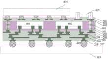
如图11~图15所示,最后进行步骤10),提供存储芯片404及被动组件405,将所述存储芯片404及所述被动组件405接合于所述连接布线层60,以实现与所述连接布线层60的电性连接。As shown in FIG. 11 to FIG. 15 , step 10) is finally performed, a
例如,可以先先采用激光工艺于所述第一绝缘层中形成窗口104,然后采用固晶工艺将所述存储芯片404接合于所述连接布线层60,如图11及图12所示,然后采用表面贴装工艺将所述被动组件405接合于所述连接布线层60,如图13所示,最后采用点胶工艺于所述存储芯片404与所述连接布线层60形成隔离保护层403,进行切割后去除所述贴膜103,如图14所示。For example, the
在本实施例中,所述被动组件405包括多个被动元件,所述多个被动元件可以呈平行阵列排布,如图15所示,所述被动元件可以为电阻、电容及电感中的一种。In this embodiment, the
所述系统级芯片401、电源管理芯片402、存储芯片404及被动组件405通过所述重新布线层20、连接布线层60及金属连接柱301实现互连,并通过所述金属凸块105实现扇出型封装。The system-on-
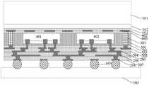
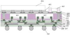
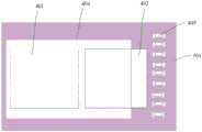
图14显示为本实施例的扇出型系统级封装结构的截面结构示意图,图15显示为本实施例的扇出型系统级封装结构的平面布局示意图,如图14~图15所示,在一具体的实施过程中,所述扇出型系统级封装结构的整体尺寸(长×宽)可以为13mm×16mm,总高度为1mm,所述系统级芯片401的尺寸(长×宽)可以为8.2×8.3mm,所述电源管理芯片402的尺寸可以为5.1mm×4.8mm,所述系统级芯片401与所述电源管理芯片402的间距为0.5mm,所述存储芯片404的厚度为0.68mm。FIG. 14 shows a schematic cross-sectional structure diagram of the fan-out system-in-package structure of this embodiment, and FIG. 15 shows a schematic plan layout of the fan-out system-in-package structure of this embodiment. As shown in FIGS. 14 to 15 , in In a specific implementation process, the overall size (length×width) of the fan-out system-in-package structure may be 13mm×16mm, and the overall height is 1mm, and the size (length×width) of the system-on-
本发明采用扇出型系统级封装将多种功能的芯片,包括系统级芯片401、电源管理芯片402、存储芯片404及被动组件405等整合在一个封装结构中,可实现多种不同的系统功能需求,提高封装系统的性能。本发明通过重新布线层及金属连接柱301,实现了系统级芯片401、电源管理芯片402、存储芯片404及被动组件405的三维垂直堆叠封装,有效降低封装系统的面积,提高封装系统的集成度。本发明通过金属连接柱301实现重新布线层之间的紧密连接,可有效短芯片之间的传导路径,降低封装系统的功耗,金属连接柱可以通过电镀工艺形成,可以有效增加金属连接柱的宽度,进一步提高传导能力。本发明的扇出型系统级封装结构,可以实现1毫米以下的封装厚度,相比于传统的SiP封装结构来说,大大降低了封装系统的整体厚度。The present invention adopts fan-out type system-in-package to integrate chips with multiple functions, including system-on-
如图14及图15所示,本实施例还提供一种扇出型系统级封装结构,所述封装结构包括:重新布线层20,所述重新布线层20包括第一面以及相对的第二面,所述重新布线层20的第一面显露有金属布线层;金属凸块105,形成于所述重新布线层20的第一面的所述金属布线层上,以实现所述重新布线层20的电性引出;金属连接柱301,形成于所述重新布线层20的第二面上,所述金属连接柱301与所述重新布线层20电性相连;系统级芯片401以及电源管理芯片402,所述系统级芯片401以及电源管理芯片402接合于所述重新布线层20的第二面上,以实现与所述重新布线层20的电性连接;封装层501,覆盖于所述金属连接柱301、系统级芯片401以及电源管理芯片402,且所述金属连接柱301显露于所述封装层501;连接布线层60,形成于所述封装层501上,所述连接布线层60与所述金属连接柱301电性连接;存储芯片404及被动组件405,接合于所述连接布线层60,以实现与所述连接布线层60的电性连接。As shown in FIG. 14 and FIG. 15 , this embodiment further provides a fan-out system-in-package structure, the package structure includes: a
所述重新布线层20包括:图形化的第一介质层201;图形化的第一金属布线层202,位于所述图形化的第一介质层201上,所述第一金属布线层202与所述金属连接柱301、所述系统级芯片401以及所述电源管理芯片402连接;图形化的第二介质层203,位于所述第一金属布线层202上;图形化的第二金属布线层204,位于所述第二介质层203上。所述介质层的材料包括环氧树脂、硅胶、PI、PBO、BCB、氧化硅、磷硅玻璃,含氟玻璃中的一种或两种以上组合,所述金属布线层的材料包括铜、铝、镍、金、银、钛中的一种或两种以上组合。在本实施例中,所述第一介质层201及第二介质层203的材料选用为PI(聚酰亚胺),以进一步降低工艺难度以及工艺成本。所述重新布线层20还可以包括更多的介质层以及金属层,以实现不同的布线功能。例如,在本实施例中,所述重新布线层20还包括图形化的第三介质层205、图形化的第三金属布线层206、图形化的第四介质层207及图形化的第四金属布线层208,所述图形化的第四金属布线层208显露于所述重新布线层20表面。The
所述金属连接柱301可以垂直于所述重新布线层20设置,以缩短传导路径,所述金属连接柱301为Au、Ag、Cu、Al中的一种,在本实施例中,所述金属连接柱301可以为铜,以提高其稳定性和降低阻抗。The
所述连接布线层60包括:图形化的第一绝缘层601;图形化的布线层602,形成于所述第一绝缘层上601,所述布线层602与所述金属连接柱301电性连接;图形化的第二绝缘层603,形成于所述布线层602上,所述金属连接柱301穿过所述第二绝缘层603与所述布线层602连接。所述第一绝缘层601中具有窗口104,所述窗口104显露所述布线层602,所述存储芯片404与所述被动组件405通过所述窗口104与所述布线层602连接。The
可选地,所述第二绝缘层603中形成有显露所述布线层的通孔,所述金属连接柱301通过电镀工艺形成于所述所述通孔。Optionally, a through hole for exposing the wiring layer is formed in the second insulating
所述系统级芯片401可以为用于手机、平板或其他智能设备的GPU芯片等。所述存储芯片404包括ePoP存储器。所述存储芯片404与所述连接布线层60之间还具有隔离保护层406。The system-on-
所述系统级芯片401与所述重新布线层20之间以及所述电源管理芯片402通过绝缘胶与所述重新布线层20连接。The system-on-
如图15所示,所述被动组件405包括多个被动元件,所述被动元件包括电阻、电容及电感中的一种。As shown in FIG. 15 , the
所述封装层501的材料包括聚酰亚胺、硅胶以及环氧树脂中的一种。所述封装层501的顶面超出所述系统级芯片401以及电源管理芯片402的顶面的厚度介于0微米~10微米。例如,该厚度可以为3微米或5微米等,当然,为了进一步减小封装结构的厚度,该厚度也可以设置为0微米,即所述封装层501顶面与所述系统级芯片401以及电源管理芯片402的顶面齐平。The material of the
所述金属凸块105包括锡焊料、银焊料及金锡合金焊料中的一种。The metal bumps 105 include one of tin solder, silver solder and gold-tin alloy solder.
所述扇出型系统级封装结构的厚度不大于1毫米。The thickness of the fan-out system-in-package structure is not more than 1 mm.
图14显示为本实施例的扇出型系统级封装结构的截面结构示意图,图15显示为本实施例的扇出型系统级封装结构的平面布局示意图,如图14~图15所示,在一具体的实施过程中,所述扇出型系统级封装结构的整体尺寸(长×宽)可以为13mm×16mm,总高度为1mm,所述系统级芯片401的尺寸(长×宽)可以为8.2×8.3mm,所述电源管理芯片402的尺寸可以为5.1mm×4.8mm,所述系统级芯片401与所述电源管理芯片402的间距为0.5mm,所述存储芯片404的厚度为0.68mm。FIG. 14 shows a schematic cross-sectional structure diagram of the fan-out system-in-package structure of this embodiment, and FIG. 15 shows a schematic plan layout of the fan-out system-in-package structure of this embodiment. As shown in FIGS. 14 to 15 , in In a specific implementation process, the overall size (length×width) of the fan-out system-in-package structure may be 13mm×16mm, and the overall height is 1mm, and the size (length×width) of the system-on-
如上所述,本发明的扇出型系统级封装结构及其制作方法,具有以下有益效果:As described above, the fan-out system-in-package structure and the manufacturing method thereof of the present invention have the following beneficial effects:
本发明采用扇出型系统级封装将多种功能的芯片,包括系统级芯片、电源管理芯片、存储芯片及被动组件等整合在一个封装结构中,可实现多种不同的系统功能需求,提高封装系统的性能。The invention adopts fan-out type system-level packaging to integrate chips with multiple functions, including system-level chips, power management chips, memory chips and passive components, etc. system performance.
本发明通过重新布线层及金属连接柱,实现了系统级芯片、电源管理芯片、存储芯片及被动组件的三维垂直堆叠封装,有效降低封装系统的面积,提高封装系统的集成度。The invention realizes the three-dimensional vertical stacking packaging of system-level chips, power management chips, memory chips and passive components by rewiring layers and metal connection posts, effectively reducing the area of the packaging system and improving the integration of the packaging system.
本发明通过金属连接柱实现重新布线层之间的紧密连接,可有效短芯片之间的传导路径,降低封装系统的功耗。金属连接柱可以通过电镀工艺形成,可以有效增加金属连接柱的宽度,进一步提高传导能力。The invention realizes the tight connection between the re-wiring layers through the metal connection post, which can effectively shorten the conduction path between the chips and reduce the power consumption of the packaging system. The metal connecting column can be formed by an electroplating process, which can effectively increase the width of the metal connecting column and further improve the conductivity.
本发明的扇出型系统级封装结构,可以实现1毫米以下的封装厚度,相比于传统的SiP封装结构来说,大大降低了封装系统的整体厚度。The fan-out type system-level packaging structure of the present invention can achieve a packaging thickness of less than 1 mm, which greatly reduces the overall thickness of the packaging system compared with the traditional SiP packaging structure.
所以,本发明有效克服了现有技术中的种种缺点而具高度产业利用价值。Therefore, the present invention effectively overcomes various shortcomings in the prior art and has high industrial utilization value.
上述实施例仅例示性说明本发明的原理及其功效,而非用于限制本发明。任何熟悉此技术的人士皆可在不违背本发明的精神及范畴下,对上述实施例进行修饰或改变。因此,举凡所属技术领域中具有通常知识者在未脱离本发明所揭示的精神与技术思想下所完成的一切等效修饰或改变,仍应由本发明的权利要求所涵盖。The above-mentioned embodiments merely illustrate the principles and effects of the present invention, but are not intended to limit the present invention. Anyone skilled in the art can modify or change the above embodiments without departing from the spirit and scope of the present invention. Therefore, all equivalent modifications or changes made by those with ordinary knowledge in the technical field without departing from the spirit and technical idea disclosed in the present invention should still be covered by the claims of the present invention.
Claims (23)
Priority Applications (1)
| Application Number | Priority Date | Filing Date | Title |
|---|---|---|---|
| CN202010285803.1ACN111370386A (en) | 2020-04-13 | 2020-04-13 | Fan-out system-in-package structure and method of making the same |
Applications Claiming Priority (1)
| Application Number | Priority Date | Filing Date | Title |
|---|---|---|---|
| CN202010285803.1ACN111370386A (en) | 2020-04-13 | 2020-04-13 | Fan-out system-in-package structure and method of making the same |
Publications (1)
| Publication Number | Publication Date |
|---|---|
| CN111370386Atrue CN111370386A (en) | 2020-07-03 |
Family
ID=71210787
Family Applications (1)
| Application Number | Title | Priority Date | Filing Date |
|---|---|---|---|
| CN202010285803.1APendingCN111370386A (en) | 2020-04-13 | 2020-04-13 | Fan-out system-in-package structure and method of making the same |
Country Status (1)
| Country | Link |
|---|---|
| CN (1) | CN111370386A (en) |
Cited By (6)
| Publication number | Priority date | Publication date | Assignee | Title |
|---|---|---|---|---|
| CN112289742A (en)* | 2020-11-20 | 2021-01-29 | 中芯长电半导体(江阴)有限公司 | Wafer system level three-dimensional fan-out type packaging structure and manufacturing method thereof |
| CN112435981A (en)* | 2020-09-30 | 2021-03-02 | 日月光半导体制造股份有限公司 | Semiconductor package device and method of manufacturing the same |
| CN112992806A (en)* | 2021-01-25 | 2021-06-18 | 日月光半导体制造股份有限公司 | Semiconductor package device and method of manufacturing the same |
| CN114975415A (en)* | 2022-04-29 | 2022-08-30 | 盛合晶微半导体(江阴)有限公司 | Fan-out stacked semiconductor packaging structure and packaging method thereof |
| WO2023087847A1 (en)* | 2021-11-19 | 2023-05-25 | 华天科技(昆山)电子有限公司 | Ultra-thin fan-out package structure for chip and manufacturing method therefor |
| WO2025015743A1 (en)* | 2023-07-20 | 2025-01-23 | 盛合晶微半导体(江阴)有限公司 | 2.5d packaging structure capable of improving power supply signal transmission, and preparation method therefor |
Citations (7)
| Publication number | Priority date | Publication date | Assignee | Title |
|---|---|---|---|---|
| US20130168856A1 (en)* | 2011-12-28 | 2013-07-04 | Taiwan Semiconductor Manufacturing Company, Ltd. | Package on Package Devices and Methods of Packaging Semiconductor Dies |
| CN103295925A (en)* | 2012-03-02 | 2013-09-11 | 新科金朋有限公司 | Semiconductor device and method for forming low profile embedded wafer level ball grid array molded laser package |
| US20130313699A1 (en)* | 2011-03-22 | 2013-11-28 | Yujuan Tao | Fan-out high-density packaging methods and structures |
| CN107104090A (en)* | 2017-05-15 | 2017-08-29 | 中芯长电半导体(江阴)有限公司 | Re-wiring layer, the encapsulating structure with the re-wiring layer and preparation method |
| CN107195551A (en)* | 2017-07-05 | 2017-09-22 | 中芯长电半导体(江阴)有限公司 | Fan-out-type laminated packaging structure and preparation method thereof |
| US20200043853A1 (en)* | 2018-07-31 | 2020-02-06 | Samsung Electronics Co., Ltd. | Semiconductor package including interposer |
| CN211980611U (en)* | 2020-04-13 | 2020-11-20 | 中芯长电半导体(江阴)有限公司 | Fan-out type system-in-package structure |
- 2020
- 2020-04-13CNCN202010285803.1Apatent/CN111370386A/enactivePending
Patent Citations (7)
| Publication number | Priority date | Publication date | Assignee | Title |
|---|---|---|---|---|
| US20130313699A1 (en)* | 2011-03-22 | 2013-11-28 | Yujuan Tao | Fan-out high-density packaging methods and structures |
| US20130168856A1 (en)* | 2011-12-28 | 2013-07-04 | Taiwan Semiconductor Manufacturing Company, Ltd. | Package on Package Devices and Methods of Packaging Semiconductor Dies |
| CN103295925A (en)* | 2012-03-02 | 2013-09-11 | 新科金朋有限公司 | Semiconductor device and method for forming low profile embedded wafer level ball grid array molded laser package |
| CN107104090A (en)* | 2017-05-15 | 2017-08-29 | 中芯长电半导体(江阴)有限公司 | Re-wiring layer, the encapsulating structure with the re-wiring layer and preparation method |
| CN107195551A (en)* | 2017-07-05 | 2017-09-22 | 中芯长电半导体(江阴)有限公司 | Fan-out-type laminated packaging structure and preparation method thereof |
| US20200043853A1 (en)* | 2018-07-31 | 2020-02-06 | Samsung Electronics Co., Ltd. | Semiconductor package including interposer |
| CN211980611U (en)* | 2020-04-13 | 2020-11-20 | 中芯长电半导体(江阴)有限公司 | Fan-out type system-in-package structure |
Cited By (7)
| Publication number | Priority date | Publication date | Assignee | Title |
|---|---|---|---|---|
| CN112435981A (en)* | 2020-09-30 | 2021-03-02 | 日月光半导体制造股份有限公司 | Semiconductor package device and method of manufacturing the same |
| CN112289742A (en)* | 2020-11-20 | 2021-01-29 | 中芯长电半导体(江阴)有限公司 | Wafer system level three-dimensional fan-out type packaging structure and manufacturing method thereof |
| CN112992806A (en)* | 2021-01-25 | 2021-06-18 | 日月光半导体制造股份有限公司 | Semiconductor package device and method of manufacturing the same |
| CN112992806B (en)* | 2021-01-25 | 2025-10-03 | 日月光半导体制造股份有限公司 | Semiconductor packaging device and manufacturing method thereof |
| WO2023087847A1 (en)* | 2021-11-19 | 2023-05-25 | 华天科技(昆山)电子有限公司 | Ultra-thin fan-out package structure for chip and manufacturing method therefor |
| CN114975415A (en)* | 2022-04-29 | 2022-08-30 | 盛合晶微半导体(江阴)有限公司 | Fan-out stacked semiconductor packaging structure and packaging method thereof |
| WO2025015743A1 (en)* | 2023-07-20 | 2025-01-23 | 盛合晶微半导体(江阴)有限公司 | 2.5d packaging structure capable of improving power supply signal transmission, and preparation method therefor |
Similar Documents
| Publication | Publication Date | Title |
|---|---|---|
| CN111370387A (en) | Fan-out type system-in-package structure and manufacturing method thereof | |
| CN111370385B (en) | Fan-out system-level packaging structure and manufacturing method thereof | |
| CN108511400B (en) | Antenna packaging structure and packaging method | |
| CN111370386A (en) | Fan-out system-in-package structure and method of making the same | |
| CN211480019U (en) | Fan-out type system-in-package structure | |
| CN107507821A (en) | The encapsulating structure and method for packing of integrated image sensor chip and logic chip | |
| CN212392240U (en) | Fan-out type packaging structure | |
| WO2018171099A1 (en) | Encapsulation method for encapsulation structure with integrated power transmission chip | |
| CN212084995U (en) | Wafer level package structure | |
| CN112289743A (en) | A wafer system-level fan-out package structure and method of making the same | |
| CN114188227B (en) | Fan-out packaging structure and packaging method | |
| CN110085973A (en) | Antenna packages structure and packaging method | |
| WO2018171100A1 (en) | Encapsulation method for encapsulation structure with integrated power transmission chip | |
| CN112289742A (en) | Wafer system level three-dimensional fan-out type packaging structure and manufacturing method thereof | |
| US11894357B2 (en) | System-level packaging structure and method for LED chip | |
| CN114188226A (en) | Fan-out packaging structure and packaging method | |
| CN114188225B (en) | Fan-out packaging structure and packaging method | |
| WO2024051225A1 (en) | Fan-out system-in-package structure, and manufacturing method therefor | |
| CN211980611U (en) | Fan-out type system-in-package structure | |
| CN110047820B (en) | Antenna packaging structure with air cavity and packaging method | |
| CN211480020U (en) | Fan-out type system-in-package structure | |
| CN212303700U (en) | System-in-package structure of LED chip | |
| CN107425031A (en) | The encapsulating structure and method for packing of back-illuminated type cmos sensor | |
| CN213242537U (en) | Wafer system level three-dimensional fan-out type packaging structure | |
| CN112151394A (en) | Packaging structure and packaging method of three-dimensional fan-out fingerprint identification chip |
Legal Events
| Date | Code | Title | Description |
|---|---|---|---|
| PB01 | Publication | ||
| PB01 | Publication | ||
| SE01 | Entry into force of request for substantive examination | ||
| SE01 | Entry into force of request for substantive examination | ||
| CB02 | Change of applicant information | Address after:No.78 Changshan Avenue, Jiangyin City, Wuxi City, Jiangsu Province (place of business: No.9 Dongsheng West Road, Jiangyin City) Applicant after:Shenghejing micro semiconductor (Jiangyin) Co.,Ltd. Address before:No.78 Changshan Avenue, Jiangyin City, Wuxi City, Jiangsu Province Applicant before:SJ Semiconductor (Jiangyin) Corp. | |
| CB02 | Change of applicant information |