CN111364025A - An improved ALD coating machine - Google Patents
An improved ALD coating machineDownload PDFInfo
- Publication number
- CN111364025A CN111364025ACN202010385822.1ACN202010385822ACN111364025ACN 111364025 ACN111364025 ACN 111364025ACN 202010385822 ACN202010385822 ACN 202010385822ACN 111364025 ACN111364025 ACN 111364025A
- Authority
- CN
- China
- Prior art keywords
- ald
- placement
- coating machine
- improved
- cavity
- Prior art date
- Legal status (The legal status is an assumption and is not a legal conclusion. Google has not performed a legal analysis and makes no representation as to the accuracy of the status listed.)
- Pending
Links
Images

Classifications
- C—CHEMISTRY; METALLURGY
- C23—COATING METALLIC MATERIAL; COATING MATERIAL WITH METALLIC MATERIAL; CHEMICAL SURFACE TREATMENT; DIFFUSION TREATMENT OF METALLIC MATERIAL; COATING BY VACUUM EVAPORATION, BY SPUTTERING, BY ION IMPLANTATION OR BY CHEMICAL VAPOUR DEPOSITION, IN GENERAL; INHIBITING CORROSION OF METALLIC MATERIAL OR INCRUSTATION IN GENERAL
- C23C—COATING METALLIC MATERIAL; COATING MATERIAL WITH METALLIC MATERIAL; SURFACE TREATMENT OF METALLIC MATERIAL BY DIFFUSION INTO THE SURFACE, BY CHEMICAL CONVERSION OR SUBSTITUTION; COATING BY VACUUM EVAPORATION, BY SPUTTERING, BY ION IMPLANTATION OR BY CHEMICAL VAPOUR DEPOSITION, IN GENERAL
- C23C16/00—Chemical coating by decomposition of gaseous compounds, without leaving reaction products of surface material in the coating, i.e. chemical vapour deposition [CVD] processes
- C23C16/44—Chemical coating by decomposition of gaseous compounds, without leaving reaction products of surface material in the coating, i.e. chemical vapour deposition [CVD] processes characterised by the method of coating
- C23C16/455—Chemical coating by decomposition of gaseous compounds, without leaving reaction products of surface material in the coating, i.e. chemical vapour deposition [CVD] processes characterised by the method of coating characterised by the method used for introducing gases into reaction chamber or for modifying gas flows in reaction chamber
- C23C16/45523—Pulsed gas flow or change of composition over time
- C23C16/45525—Atomic layer deposition [ALD]
- C—CHEMISTRY; METALLURGY
- C23—COATING METALLIC MATERIAL; COATING MATERIAL WITH METALLIC MATERIAL; CHEMICAL SURFACE TREATMENT; DIFFUSION TREATMENT OF METALLIC MATERIAL; COATING BY VACUUM EVAPORATION, BY SPUTTERING, BY ION IMPLANTATION OR BY CHEMICAL VAPOUR DEPOSITION, IN GENERAL; INHIBITING CORROSION OF METALLIC MATERIAL OR INCRUSTATION IN GENERAL
- C23C—COATING METALLIC MATERIAL; COATING MATERIAL WITH METALLIC MATERIAL; SURFACE TREATMENT OF METALLIC MATERIAL BY DIFFUSION INTO THE SURFACE, BY CHEMICAL CONVERSION OR SUBSTITUTION; COATING BY VACUUM EVAPORATION, BY SPUTTERING, BY ION IMPLANTATION OR BY CHEMICAL VAPOUR DEPOSITION, IN GENERAL
- C23C16/00—Chemical coating by decomposition of gaseous compounds, without leaving reaction products of surface material in the coating, i.e. chemical vapour deposition [CVD] processes
- C23C16/44—Chemical coating by decomposition of gaseous compounds, without leaving reaction products of surface material in the coating, i.e. chemical vapour deposition [CVD] processes characterised by the method of coating
- C23C16/458—Chemical coating by decomposition of gaseous compounds, without leaving reaction products of surface material in the coating, i.e. chemical vapour deposition [CVD] processes characterised by the method of coating characterised by the method used for supporting substrates in the reaction chamber
- C—CHEMISTRY; METALLURGY
- C23—COATING METALLIC MATERIAL; COATING MATERIAL WITH METALLIC MATERIAL; CHEMICAL SURFACE TREATMENT; DIFFUSION TREATMENT OF METALLIC MATERIAL; COATING BY VACUUM EVAPORATION, BY SPUTTERING, BY ION IMPLANTATION OR BY CHEMICAL VAPOUR DEPOSITION, IN GENERAL; INHIBITING CORROSION OF METALLIC MATERIAL OR INCRUSTATION IN GENERAL
- C23C—COATING METALLIC MATERIAL; COATING MATERIAL WITH METALLIC MATERIAL; SURFACE TREATMENT OF METALLIC MATERIAL BY DIFFUSION INTO THE SURFACE, BY CHEMICAL CONVERSION OR SUBSTITUTION; COATING BY VACUUM EVAPORATION, BY SPUTTERING, BY ION IMPLANTATION OR BY CHEMICAL VAPOUR DEPOSITION, IN GENERAL
- C23C16/00—Chemical coating by decomposition of gaseous compounds, without leaving reaction products of surface material in the coating, i.e. chemical vapour deposition [CVD] processes
- C23C16/44—Chemical coating by decomposition of gaseous compounds, without leaving reaction products of surface material in the coating, i.e. chemical vapour deposition [CVD] processes characterised by the method of coating
- C23C16/54—Apparatus specially adapted for continuous coating
Landscapes
- Chemical & Material Sciences (AREA)
- General Chemical & Material Sciences (AREA)
- Chemical Kinetics & Catalysis (AREA)
- Engineering & Computer Science (AREA)
- Materials Engineering (AREA)
- Mechanical Engineering (AREA)
- Metallurgy (AREA)
- Organic Chemistry (AREA)
- Container, Conveyance, Adherence, Positioning, Of Wafer (AREA)
- Chemical Vapour Deposition (AREA)
- Physical Vapour Deposition (AREA)
Abstract
Translated fromChinese
Description
Translated fromChinese技术领域technical field
本发明属于原子层镀膜领域,具体是一种改进型ALD镀膜机。The invention belongs to the field of atomic layer coating, in particular to an improved ALD coating machine.
背景技术Background technique
目前空间ALD(atomic layer deposition,单原子层沉积)机台普遍体积较大,且结构复杂,多片工艺的ALD机台设计如:Picosun (芬兰ALD设备供应商)都是利用金属cassette(晶圆装载盒)的方法,这种方法会导致运送晶圆十分复杂,而且不稳定,手动取片比较多,如果使用自动化的方法,经常出现掉片的现象;ASM(美国ALD设备供应商)及TEL(日本ALD设备供应商)的多片式ALD炉子方法所使用气体及前驱体使用效率低,会造成巨大的浪费。At present, space ALD (atomic layer deposition, single atomic layer deposition) machines are generally large in size and complex in structure. The design of ALD machines for multi-chip processes, such as: Picosun (Finnish ALD equipment supplier), uses metal cassettes (wafers). Loading box) method, this method will lead to very complicated and unstable transportation of wafers, and there are more manual fetches. If the automated method is used, the phenomenon of wafer drop often occurs; The gas and precursor used in the multi-chip ALD furnace method (a Japanese ALD equipment supplier) are inefficient and cause huge waste.
发明内容SUMMARY OF THE INVENTION
本发明的目的在于提供一种改进型ALD镀膜机,以解决目前市场上的ALD机台效率低的的问题。本发明提供如下技术方案:The purpose of the present invention is to provide an improved ALD coating machine to solve the problem of low efficiency of the ALD machines currently on the market. The present invention provides the following technical solutions:
一种改进型ALD镀膜机,包括在内部安装有拿持结构的传送放置通道,和多个放置腔体;An improved ALD coating machine, comprising a transfer placement channel with a holding structure installed inside, and a plurality of placement cavities;
其中,所述拿持结构可对位于传送放置通道内部的晶圆拿持取放到多个放置腔体内部的盒体中,营造真空环境后可对盒体及晶圆进行翻转;Wherein, the holding structure can hold and place the wafers located inside the conveying and placing channels into the boxes inside the multiple placement cavities, and the boxes and the wafers can be turned over after creating a vacuum environment;
还包括多个ALD反应器,而放置腔体内部的晶圆移动到ALD反应器中进行单原子层沉积工艺反应;It also includes a plurality of ALD reactors, and the wafers placed inside the chamber are moved to the ALD reactors for single atomic layer deposition process reactions;
进而,拿持结构对位于传送放置通道内部的晶圆拿持取放到多个放置腔体内部的盒体中,营造真空环境后对盒体及晶圆进行翻转并移动到ALD反应器中进行单原子层沉积工艺反应,进行镀膜;以及多个放置腔体和多个ALD反应器可同时进行多个晶圆镀膜,效率得以提高;同时,可对多个ALD反应器做不同的介电常数材料的生长,实现了多种材料工艺交替的镀膜处理,无需更换生产线,提高效率的基础上节省生产线的成本。Furthermore, the holding structure holds and places the wafers located inside the conveying and placing channels into the boxes inside the multiple placement cavities. After creating a vacuum environment, the boxes and wafers are turned over and moved to the ALD reactor for processing. The single atomic layer deposition process reacts and performs coating; and multiple placement cavities and multiple ALD reactors can simultaneously perform multiple wafer coating, and the efficiency is improved; at the same time, multiple ALD reactors can be used for different dielectric constants The growth of the material realizes the alternate coating treatment of various material processes, without the need to replace the production line, and saves the cost of the production line on the basis of improving the efficiency.
本发明中:所述拿持结构包括机械手,以用晶圆取放。In the present invention, the holding structure includes a manipulator to pick and place wafers.
再进一步的方案:所述拿持结构还包括机械人,机械手安装在机器人上,并利用机械手对可对位于传送放置通道内部的晶圆拿持取放到多个放置腔体内部的盒体中。Still a further solution: the holding structure further includes a robot, the robot arm is installed on the robot, and the robot arm is used to hold and place the wafers located inside the transfer and placement channel into the boxes inside the multiple placement cavities. .
本发明中:所述放置腔体内部盒体及晶圆进行50-120度的翻转。In the present invention, the box body and the wafer inside the placement cavity are turned over by 50-120 degrees.
再进一步的方案:所述放置腔体内部盒体及晶圆进行90度的翻转。A further solution: the inner box and the wafer in the placement cavity are turned over by 90 degrees.
本发明中:多个所述放置腔体为独立设置,并连通到ALD反应器,以用晶圆移动调整。In the present invention, a plurality of the placement cavities are independently arranged and communicated with the ALD reactor for adjustment by wafer movement.
本发明中:多个所述ALD反应器为分开设置,用以分开完成镀膜。In the present invention, a plurality of the ALD reactors are arranged separately to complete the coating separately.
本发明中:所述改进型ALD镀膜机,还包括翻转升降机构,所述翻转升降机构设置在放置腔体内部,并完成将放置腔体内部的晶圆移动到ALD反应器中进行单原子层沉积工艺反应。In the present invention, the improved ALD coating machine further includes an inversion lifting mechanism, which is arranged inside the placement cavity and completes the movement of the wafer inside the placement cavity into the ALD reactor for monoatomic layering Deposition process reaction.
本发明中:所述传送放置通道上设置有多个用于放置晶圆的装载盒。In the present invention, a plurality of loading boxes for placing wafers are arranged on the conveying and placing channel.
本发明中:所述放置腔体内部安装有用于形成真空的抽真空设备。In the present invention, a vacuuming device for forming a vacuum is installed inside the placing cavity.
因此,本发明改进型ALD镀膜机,包括在内部安装有拿持结构的传送放置通道,和多个放置腔体;其中,所述拿持结构可对位于传送放置通道内部的晶圆拿持取放到多个放置腔体内部的盒体中,营造真空环境后可对盒体及晶圆进行翻转;还包括多个ALD反应器,而放置腔体内部的晶圆移动到ALD反应器中进行单原子层沉积工艺反应;拿持结构对位于传送放置通道内部的晶圆拿持取放到多个放置腔体内部的盒体中,营造真空环境后对晶圆翻转并移动到ALD反应器中进行单原子层沉积工艺反应,进行镀膜;以及多个放置腔体和多个ALD反应器可同时进行多个晶圆镀膜,效率得以提高;同时,可对多个ALD反应器做不同的介电常数材料的生长,实现了多种材料工艺交替的镀膜处理,无需更换生产线,提高效率的基础上节省生产线的成本。Therefore, the improved ALD coating machine of the present invention includes a transfer and placement channel with a holding structure installed inside, and a plurality of placement cavities; wherein, the holding structure can hold the wafer located in the transfer and placement channel. It is placed in multiple boxes placed inside the cavity, and the boxes and wafers can be turned over after creating a vacuum environment; it also includes multiple ALD reactors, and the wafers placed inside the cavity are moved to the ALD reactor for processing. The single atomic layer deposition process reaction; the holding structure holds the wafers located inside the transfer and placement channels and places them in boxes inside multiple placement chambers, and after creating a vacuum environment, the wafers are turned over and moved to the ALD reactor Single atomic layer deposition process reaction, coating; and multiple placement chambers and multiple ALD reactors can simultaneously conduct multiple wafer coating, and the efficiency is improved; at the same time, multiple ALD reactors can be made with different dielectrics The growth of constant materials realizes the alternate coating treatment of various material processes, without the need to replace the production line, and saves the cost of the production line on the basis of improving efficiency.
附图说明Description of drawings
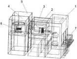
图1为本发明改进型ALD镀膜机的结构示意图。Fig. 1 is the structural schematic diagram of the improved ALD coating machine of the present invention.
图2为图1中机械人和金属盒体的装配结构示意图。FIG. 2 is a schematic diagram of the assembly structure of the robot and the metal box in FIG. 1 .
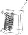
图3为图1中塑料盒体的结构示意图。FIG. 3 is a schematic structural diagram of the plastic box body in FIG. 1 .
图中:1-传送放置通道;2-放置腔体Ⅰ;3-放置腔体Ⅱ;4-ALD反应器Ⅰ;5-ALD反应器Ⅱ;6-金属盒体;7-塑料盒体。In the figure: 1-transmission and placement channel; 2-placement cavity I; 3-placement cavity II; 4-ALD reactor I; 5-ALD reactor II; 6-metal box; 7-plastic box.
具体实施方式Detailed ways
本发明的目的在于提供一种改进型ALD镀膜机,以解决目前市场上的ALD机台效率低的的问题。本发明提供如下技术方案:The purpose of the present invention is to provide an improved ALD coating machine to solve the problem of low efficiency of the ALD machines currently on the market. The present invention provides the following technical solutions:
本发明实施例中,如图1所示,一种改进型ALD镀膜机,包括在内部安装有拿持结构的传送放置通道1,和多个放置腔体;In the embodiment of the present invention, as shown in FIG. 1 , an improved ALD coating machine includes a
其中,所述拿持结构可对位于传送放置通道1内部的晶圆拿持取放到多个放置腔体内部的盒体中,营造真空环境后对盒体及晶圆进行翻转;Wherein, the holding structure can hold and place the wafers located inside the conveying and placing
还包括多个ALD反应器,而放置腔体内部晶圆移动到ALD反应器中进行单原子层沉积工艺反应;It also includes a plurality of ALD reactors, and the wafers inside the chamber are placed and moved to the ALD reactors for single atomic layer deposition process reactions;
本发明实施例中,拿持结构对位于传送放置通道1内部的晶圆拿持取放到多个放置腔体内部的盒体中,营造真空环境后对盒体及晶圆进行翻转并移动到ALD反应器中进行单原子层沉积工艺反应,进行镀膜;以及多个放置腔体和多个ALD反应器可同时进行多个晶圆镀膜,效率得以提高;同时,可对多个ALD反应器做不同的介电常数材料的生长,实现了多种材料工艺交替的镀膜处理,无需更换生产线,提高效率的基础上节省生产线的成本。In the embodiment of the present invention, the holding structure holds and places the wafers located inside the transfer and
本发明实施例中,如图1和图2所示,所述拿持结构包括机械手,以用晶圆取放;进一步的优化,所述拿持结构还包括机械人,机械手安装在机器人上,并利用机械手对可对位于传送放置通道1内部的晶圆拿持取放到多个放置腔体内部的盒体中。其中,机械手可替换为夹持机构、或者托举机构,具体为哪种结构不作限制只要能满足利用该结构对可对位于传送放置通道1内部的晶圆拿持取放到多个放置腔体内部的盒体中即可;优选机械手。In the embodiment of the present invention, as shown in FIG. 1 and FIG. 2 , the holding structure includes a manipulator to pick and place wafers; for further optimization, the holding structure further includes a robot, and the manipulator is installed on the robot, The wafers located inside the conveying and placing
本发明实施例中,如图1所示,所述放置腔体内部的盒体及晶圆进行50-120度的翻转;进一步的优化,所述放置腔体内部的盒体及晶圆进行90度的翻转。盒体可对晶圆进行的角度翻转的范围不作限制,只要能满足翻转后盒体将晶圆移动到ALD反应器中进行单原子层沉积工艺反应即可;其中,可对晶圆进行90度的翻转可以很好的进行翻转后,对晶圆整体移动到ALD反应器中进行单原子层沉积工艺反应。In the embodiment of the present invention, as shown in FIG. 1 , the box body and the wafer inside the placement cavity are turned over by 50-120 degrees; for further optimization, the box body and the wafer inside the placement cavity are rotated 90 degrees. degree of reversal. The range of the angle that the box body can flip the wafer is not limited, as long as the box body can move the wafer to the ALD reactor for the single atomic layer deposition process reaction after the flip; among them, the wafer can be rotated 90 degrees. The flipping can be done well after flipping, and the whole wafer is moved to the ALD reactor for single atomic layer deposition process reaction.
本发明实施例中,如图1所示,多个所述放置腔体为独立设置,并连通到ALD反应器,用以晶圆移动调整。其中,多个可以是2个、3个、4个.....,具体为多少不作限制,只要能满足独立设置,并连通到ALD反应器,以用晶圆移动调整即可;优化的,所述放置腔体设置有两个分别为放置腔体Ⅰ2和放置腔体Ⅱ3,放置腔体Ⅰ2和放置腔体Ⅱ3形成了独立的双腔,并连通到ALD反应器,以用晶圆移动调整。In the embodiment of the present invention, as shown in FIG. 1 , a plurality of the placement cavities are independently arranged and connected to the ALD reactor for adjustment of the movement of the wafer. Among them, the number of multiples can be 2, 3, 4..., the number is not limited, as long as the independent setting can be satisfied, and it can be connected to the ALD reactor for adjustment by wafer movement; the optimized , the placement cavity is provided with two placement cavity I2 and placement cavity II3, the placement cavity I2 and placement cavity II3 form an independent double cavity, and are connected to the ALD reactor to move the wafer with Adjustment.
本发明实施例中,如图1所示,多个所述ALD反应器为分开设置,用以分开完成镀膜。其中,多个可以是2个、3个、4个.....,具体为多少不作限制,只要能满足分开完成镀膜即可;优化的,所述ALD反应器设置有两个,分别为ALD反应器Ⅰ4和ALD反应器Ⅱ5,ALD反应器Ⅰ4和ALD反应器Ⅱ5可以分开完成镀膜,可分别对ALD反应器Ⅰ4和ALD反应器Ⅱ5做高介电常数(HK)和低介电常数材料(LK)的生长,实现了多种材料工艺交替的镀膜处理,无需更换生产线,提高效率的基础上节省生产线的成本。In the embodiment of the present invention, as shown in FIG. 1 , a plurality of the ALD reactors are arranged separately to complete the coating separately. Among them, the number of multiples can be 2, 3, 4..., the specific number is not limited, as long as the coating can be completed separately; optimized, the ALD reactor is provided with two, respectively ALD Reactor I4 and ALD Reactor II5, ALD Reactor I4 and ALD Reactor II5 can complete the coating separately, and can be used for ALD Reactor I4 and ALD Reactor II5 respectively. High dielectric constant (HK) and low dielectric constant materials The growth of (LK) realizes the alternate coating treatment of various material processes, without the need to replace the production line, and saves the cost of the production line on the basis of improving efficiency.
本发明实施例中,如图1所示,所述改进型ALD镀膜机,还包括翻转升降机构,所述翻转升降机构设置在放置腔体内部,并完成将放置腔体内部的盒体及晶圆移动到ALD反应器中进行单原子层沉积工艺反应。其中,翻转升降机构可以是气缸,也是液压缸,或者是电机带动的螺纹杆和螺母实现的螺纹传动升降等等;具体为哪种结构不作限制只要能满足完成将放置腔体内部的晶圆整体移动到ALD反应器中进行单原子层沉积工艺反应即可。In the embodiment of the present invention, as shown in FIG. 1 , the improved ALD coating machine further includes an overturning and lifting mechanism, and the overturning and lifting mechanism is arranged inside the placement cavity, and completes the placement of the box and the crystal inside the placement cavity. The circle moves into the ALD reactor for the monoatomic layer deposition process reaction. Among them, the overturning and lifting mechanism can be an air cylinder, a hydraulic cylinder, or a threaded drive lifting and lowering realized by a threaded rod and a nut driven by a motor, etc.; the specific structure is not limited as long as it can meet the requirements of completing the entire wafer to be placed inside the cavity. Move to the ALD reactor to carry out the single atomic layer deposition process reaction.
本发明实施例中,如图1和图3所示,所述传送放置通道1上设置有多个用于放置晶圆的装载盒,而装载盒为塑料盒体7;所述放置腔体内部的盒体为金属盒体6。其中,对于装载盒的材质和/或盒体的材质不作限制,优选的,载盒为塑料盒体7;放置腔体内部的盒体为金属盒体6。In the embodiment of the present invention, as shown in FIG. 1 and FIG. 3 , the conveying and placing
本发明实施例中,如图1所示,所述放置腔体内部安装有用于盒体对晶圆形成真空的抽真空设备。其中,用于形成真空的抽真空设备可以是单极往复泵,也可以是离心式真空干泵,具体为哪种不作限制,只要能满足用于对放置腔体形成真空即可。In the embodiment of the present invention, as shown in FIG. 1 , a vacuuming device for vacuuming the wafer by the box body is installed inside the placement cavity. Wherein, the vacuuming device used for forming the vacuum may be a unipolar reciprocating pump or a centrifugal vacuum dry pump, which is not limited, as long as it can be used to form a vacuum for the placement cavity.
本发明改进型ALD镀膜机,包括在内部安装有拿持结构的传送放置通道1,和多个放置腔体;其中,所述拿持结构可对位于传送放置通道1内部的晶圆拿持取放到多个放置腔体内部的盒体中,抽真空后可对盒体及晶圆进行翻转;还包括多个ALD反应器,放置腔体内部的盒体及晶圆被移动到ALD反应器中进行单原子层沉积工艺反应;进而,拿持结构对位于传送放置通道1内部的晶圆拿持取放到多个放置腔体内部的盒体中,营造真空环境后对晶圆翻转并移动到ALD反应器中进行单原子层沉积工艺反应,进行镀膜;以及多个放置腔体和多个ALD反应器可同时进行多个晶圆镀膜,效率得以提高;同时,可对多个ALD反应器做不同的介电常数材料的生长,实现了多种材料工艺交替的镀膜处理,无需更换生产线,提高效率的基础上节省生产线的成本。The improved ALD coating machine of the present invention includes a transfer and
上面对本发明的较佳实施方式作了详细说明,但是本发明并不限于上述实施方式,在本领域的普通技术人员所具备的知识范围内,还可以在不脱离本发明宗旨的前提下作出各种变化。The preferred embodiments of the present invention have been described in detail above, but the present invention is not limited to the above-mentioned embodiments. Within the scope of knowledge possessed by those of ordinary skill in the art, various aspects can also be made without departing from the purpose of the present invention. kind of change.
Claims (10)
Translated fromChinesePriority Applications (1)
| Application Number | Priority Date | Filing Date | Title |
|---|---|---|---|
| CN202010385822.1ACN111364025A (en) | 2020-05-09 | 2020-05-09 | An improved ALD coating machine |
Applications Claiming Priority (1)
| Application Number | Priority Date | Filing Date | Title |
|---|---|---|---|
| CN202010385822.1ACN111364025A (en) | 2020-05-09 | 2020-05-09 | An improved ALD coating machine |
Publications (1)
| Publication Number | Publication Date |
|---|---|
| CN111364025Atrue CN111364025A (en) | 2020-07-03 |
Family
ID=71205787
Family Applications (1)
| Application Number | Title | Priority Date | Filing Date |
|---|---|---|---|
| CN202010385822.1APendingCN111364025A (en) | 2020-05-09 | 2020-05-09 | An improved ALD coating machine |
Country Status (1)
| Country | Link |
|---|---|
| CN (1) | CN111364025A (en) |
Cited By (1)
| Publication number | Priority date | Publication date | Assignee | Title |
|---|---|---|---|---|
| JP2024530500A (en)* | 2021-08-13 | 2024-08-21 | ベネク・オサケユフティオ | Atomic layer deposition apparatus and loading method |
Citations (8)
| Publication number | Priority date | Publication date | Assignee | Title |
|---|---|---|---|---|
| TW200622046A (en)* | 2004-09-13 | 2006-07-01 | Genus Inc | Multi-single wafer processing apparatus |
| CN101215692A (en)* | 2008-01-04 | 2008-07-09 | 清华大学 | Multi-chamber atomic layer deposition apparatus and method |
| CN101768731A (en)* | 2008-12-29 | 2010-07-07 | K.C.科技股份有限公司 | Atomic layer deposition apparatus |
| KR101486937B1 (en)* | 2013-11-15 | 2015-01-29 | 코닉이앤씨 주식회사 | Atomic layer deposition apparatus and method thereof |
| CN105789027A (en)* | 2015-01-12 | 2016-07-20 | 朗姆研究公司 | Integrated atomic-level processes: ALD (Atomic Layer Deposition) and ALE (Atomic Layer Etching) |
| JP2017150078A (en)* | 2017-03-07 | 2017-08-31 | ピコサン オーワイPicosun Oy | Loading of substrate in ald reactor |
| US20190276934A1 (en)* | 2018-03-09 | 2019-09-12 | Asm Ip Holding B.V. | Semiconductor processing apparatus and methods for monitoring and controlling a semiconductor processing apparatus |
| CN212388110U (en)* | 2020-05-09 | 2021-01-22 | 南京原磊纳米材料有限公司 | Improved generation ALD coating machine |
- 2020
- 2020-05-09CNCN202010385822.1Apatent/CN111364025A/enactivePending
Patent Citations (8)
| Publication number | Priority date | Publication date | Assignee | Title |
|---|---|---|---|---|
| TW200622046A (en)* | 2004-09-13 | 2006-07-01 | Genus Inc | Multi-single wafer processing apparatus |
| CN101215692A (en)* | 2008-01-04 | 2008-07-09 | 清华大学 | Multi-chamber atomic layer deposition apparatus and method |
| CN101768731A (en)* | 2008-12-29 | 2010-07-07 | K.C.科技股份有限公司 | Atomic layer deposition apparatus |
| KR101486937B1 (en)* | 2013-11-15 | 2015-01-29 | 코닉이앤씨 주식회사 | Atomic layer deposition apparatus and method thereof |
| CN105789027A (en)* | 2015-01-12 | 2016-07-20 | 朗姆研究公司 | Integrated atomic-level processes: ALD (Atomic Layer Deposition) and ALE (Atomic Layer Etching) |
| JP2017150078A (en)* | 2017-03-07 | 2017-08-31 | ピコサン オーワイPicosun Oy | Loading of substrate in ald reactor |
| US20190276934A1 (en)* | 2018-03-09 | 2019-09-12 | Asm Ip Holding B.V. | Semiconductor processing apparatus and methods for monitoring and controlling a semiconductor processing apparatus |
| CN212388110U (en)* | 2020-05-09 | 2021-01-22 | 南京原磊纳米材料有限公司 | Improved generation ALD coating machine |
Cited By (1)
| Publication number | Priority date | Publication date | Assignee | Title |
|---|---|---|---|---|
| JP2024530500A (en)* | 2021-08-13 | 2024-08-21 | ベネク・オサケユフティオ | Atomic layer deposition apparatus and loading method |
Similar Documents
| Publication | Publication Date | Title |
|---|---|---|
| JP4912253B2 (en) | Substrate transport apparatus, substrate processing apparatus, and substrate transport method | |
| JP3238432B2 (en) | Multi-chamber type single wafer processing equipment | |
| JP6240678B2 (en) | Loading of substrates in ALD reactor | |
| CN102099907B (en) | Workpiece transfer system and method | |
| TWI408766B (en) | Vacuum processing device | |
| US11600503B2 (en) | High-throughput, multi-chamber substrate processing system | |
| CN106558520A (en) | Wafer transmission system and chip transmission method | |
| KR20100086490A (en) | Method for manufacturing workpieces and apparatus | |
| CN1144398A (en) | Rotary semiconductor wafer processing apparatus and semiconductor wafer processing method | |
| JP4928562B2 (en) | Robot apparatus and processing apparatus, processing system, and processing method including the same | |
| JP2020038880A (en) | Substrate conveyance mechanism, substrate processing apparatus, and substrate conveyance method | |
| CN103276369A (en) | PECVD (plasma enhanced chemical vapor deposition) film coating system | |
| CN115020308A (en) | Wafer transfer device, equipment platform system and wafer transfer method thereof | |
| CN100561666C (en) | Semiconductor technology processing system and processing method thereof | |
| CN111364025A (en) | An improved ALD coating machine | |
| CN105470169A (en) | GaN device-oriented medium growth system and operation method thereof | |
| CN212388110U (en) | Improved generation ALD coating machine | |
| JP2003037146A (en) | Semiconductor manufacturing apparatus having buffer mechanism and method | |
| JP4702867B2 (en) | Vacuum processing equipment | |
| CN105957824A (en) | Gallium nitride device medium growth method and system | |
| WO2010013333A1 (en) | Vacuum device and vacuum treatment method | |
| CN113451186B (en) | Transfer robot and substrate processing system including the same | |
| CN211529927U (en) | Silicon chip transporting device | |
| JP5832372B2 (en) | Vacuum processing equipment | |
| JPH03155619A (en) | Vacuum processing equipment |
Legal Events
| Date | Code | Title | Description |
|---|---|---|---|
| PB01 | Publication | ||
| PB01 | Publication | ||
| SE01 | Entry into force of request for substantive examination | ||
| SE01 | Entry into force of request for substantive examination | ||
| RJ01 | Rejection of invention patent application after publication | ||
| RJ01 | Rejection of invention patent application after publication | Application publication date:20200703 |