CN111352516B - Touch screen and electronic equipment - Google Patents
Touch screen and electronic equipmentDownload PDFInfo
- Publication number
- CN111352516B CN111352516BCN201811583990.0ACN201811583990ACN111352516BCN 111352516 BCN111352516 BCN 111352516BCN 201811583990 ACN201811583990 ACN 201811583990ACN 111352516 BCN111352516 BCN 111352516B
- Authority
- CN
- China
- Prior art keywords
- protective layer
- touch screen
- auxiliary block
- insulating protective
- area
- Prior art date
- Legal status (The legal status is an assumption and is not a legal conclusion. Google has not performed a legal analysis and makes no representation as to the accuracy of the status listed.)
- Active
Links
Images


Classifications
- G—PHYSICS
- G06—COMPUTING OR CALCULATING; COUNTING
- G06F—ELECTRIC DIGITAL DATA PROCESSING
- G06F3/00—Input arrangements for transferring data to be processed into a form capable of being handled by the computer; Output arrangements for transferring data from processing unit to output unit, e.g. interface arrangements
- G06F3/01—Input arrangements or combined input and output arrangements for interaction between user and computer
- G06F3/03—Arrangements for converting the position or the displacement of a member into a coded form
- G06F3/041—Digitisers, e.g. for touch screens or touch pads, characterised by the transducing means
- G—PHYSICS
- G06—COMPUTING OR CALCULATING; COUNTING
- G06F—ELECTRIC DIGITAL DATA PROCESSING
- G06F2203/00—Indexing scheme relating to G06F3/00 - G06F3/048
- G06F2203/041—Indexing scheme relating to G06F3/041 - G06F3/045
- G06F2203/04103—Manufacturing, i.e. details related to manufacturing processes specially suited for touch sensitive devices
Landscapes
- Engineering & Computer Science (AREA)
- General Engineering & Computer Science (AREA)
- Theoretical Computer Science (AREA)
- Human Computer Interaction (AREA)
- Physics & Mathematics (AREA)
- General Physics & Mathematics (AREA)
- Position Input By Displaying (AREA)
Abstract
Translated fromChinese
Description
Translated fromChinese技术领域technical field
本发明涉及触控技术领域,特别是涉及一种触摸屏及电子设备。The present invention relates to the technical field of touch control, and in particular, to a touch screen and an electronic device.
背景技术Background technique
触摸屏生产过程中,通常会在一透明基板上设置ITO层(ITO为Indium tinoxide的缩写,中文名称为氧化铟锡),并在ITO层上设置金属层,再对ITO层和金属层进行曝光、显影、蚀刻等操作后,会得到线路层(包括触控区的触控电极、边框区的电极走线以及绑定区的绑定块),后续生产中还会在线路层上覆盖一层绝缘保护层,绝缘保护层分别与线路层以及透明基板贴合。In the production process of the touch screen, an ITO layer (ITO is the abbreviation of Indium tinoxide, Chinese name is indium tin oxide) is usually arranged on a transparent substrate, and a metal layer is arranged on the ITO layer, and then the ITO layer and the metal layer are exposed, After developing, etching and other operations, the circuit layer (including the touch electrodes in the touch area, the electrode wiring in the frame area, and the binding block in the binding area) will be obtained, and a layer of insulation will be covered on the circuit layer in subsequent production. The protective layer and the insulating protective layer are respectively attached to the circuit layer and the transparent substrate.
其中,绑定区用于安装电路板,为了优化触摸屏的结构,绑定区通常向外凸出,故绑定区的背面贴设的绝缘保护层也向外凸出,由于绝缘保护层与透明基板之间的黏接性不强,故绑定区背面的绝缘保护层极易翘起,不仅影响触摸屏美观,还可能导致绝缘保护层与透明基板之间产生气泡,甚至导致绝缘保护层从基板上脱落。Among them, the binding area is used to install the circuit board. In order to optimize the structure of the touch screen, the binding area usually protrudes outward, so the insulating protective layer attached to the back of the binding area also protrudes outward. The adhesion between the substrates is not strong, so the insulating protective layer on the back of the binding area is very easy to lift, which not only affects the beauty of the touch screen, but also may cause bubbles between the insulating protective layer and the transparent substrate, and even cause the insulating protective layer to be removed from the substrate. fall off.
发明内容SUMMARY OF THE INVENTION
本发明提供一种触摸屏及电子设备,旨在解决现有触摸屏绑定区背面相应区域的绝缘保护层边缘易翘起的问题。The present invention provides a touch screen and an electronic device, aiming at solving the problem that the edge of the insulating protective layer in the corresponding area on the back of the binding area of the existing touch screen is easily lifted.
本发明是这样实现的,一种触摸屏,包括:相背设置的第一表面和第二表面;其中,所述第一表面设有用于与电路板相接的第一绑定区,所述第二表面覆盖有第一绝缘保护层;此外,所述第二表面与所述第一绑定区相对的区域设有第一辅助块,所述第一辅助块与所述绝第一缘保护层相接触,所述第一辅助块可以防止所述第一绝缘保护层的翘起。The present invention is implemented as follows: a touch screen includes: a first surface and a second surface arranged opposite to each other; wherein, the first surface is provided with a first binding area for connecting with a circuit board, the first surface Two surfaces are covered with a first insulating protective layer; in addition, a first auxiliary block is provided in the region of the second surface opposite to the first binding area, and the first auxiliary block and the insulating first protective layer In contact with each other, the first auxiliary block can prevent the lifting of the first insulating protective layer.
在本发明提供的触摸屏中,通过设置第一辅助块,使得粘贴第一绝缘保护层时,位于第一绑定区背面的第一绝缘保护层可以获取更好的黏接效果,可以更好地解决第二表面与第一绑定区相对应区域的第一绝缘保护层边缘翘起的问题,从而可以有效减少因第一绝缘保护层边缘翘起所导致的第一绝缘保护层与第二表面之间产生气泡或者第一绝缘保护层从第二表面上脱落等问题的出现,提高第一绝缘保护层粘贴的良品率。In the touch screen provided by the present invention, by arranging the first auxiliary block, when the first insulating protective layer is pasted, the first insulating protective layer located on the back of the first binding area can obtain a better bonding effect, and can better Solve the problem that the edge of the first insulating protective layer in the area corresponding to the second surface and the first binding area is lifted, so that the first insulating protective layer and the second surface caused by the lifting of the edge of the first insulating protective layer can be effectively reduced The occurrence of problems such as the generation of air bubbles or the peeling of the first insulating protective layer from the second surface improves the yield of the first insulating protective layer pasted.
进一步的,所述第一辅助块与所述第一绝缘保护层之间的黏接强度大于所述第二表面与所述第一绝缘保护层之间的黏接强度。由于第一绝缘保护层与第一辅助块之间具有更好的黏接性能,故相比于现有设计而言,本发明所提供的触摸屏,可以更好地解决第一绝缘保护层位于A区域部分的边缘翘起的问题。Further, the adhesive strength between the first auxiliary block and the first insulating protective layer is greater than the adhesive strength between the second surface and the first insulating protective layer. Since the first insulating protective layer and the first auxiliary block have better adhesion performance, compared with the existing design, the touch screen provided by the present invention can better solve the problem that the first insulating protective layer is located at A The edge of the area part is lifted.
进一步的,所述第一辅助块与所述第一绝缘保护层的边缘相接触,以便进一步降低第一绝缘保护层位于A区域的边缘翘起的可能性。Further, the first auxiliary block is in contact with the edge of the first insulating protection layer, so as to further reduce the possibility of the edge of the first insulating protection layer located in the A region being lifted.
进一步的,所述第一辅助块为ITO辅助块,ITO辅助块可以和触摸屏触控电极经同一生产工艺制成,可以减少触摸屏的生产工序,提高生产效率。Further, the first auxiliary block is an ITO auxiliary block, and the ITO auxiliary block and the touch electrode of the touch screen can be made by the same production process, which can reduce the production process of the touch screen and improve the production efficiency.
进一步的,所述触摸屏还包括设置在所述第二表面的地线,所述ITO辅助块与所述地线相接。这样可以在一定程度上增大这部分地线的宽度,提高该地线的导电能力、抗冲击能力,以及抗腐蚀能力。Further, the touch screen further includes a ground wire disposed on the second surface, and the ITO auxiliary block is connected to the ground wire. In this way, the width of this part of the ground wire can be increased to a certain extent, and the conductivity, impact resistance, and corrosion resistance of the ground wire can be improved.
进一步的,所述ITO辅助块与所述地线之间具有镂空区域,这样可以有效防止蚀刻液在蚀刻地线时出现的扩散现象,从而提高地线的抗腐蚀能力。Further, there is a hollow area between the ITO auxiliary block and the ground wire, which can effectively prevent the etchant from spreading when etching the ground wire, thereby improving the corrosion resistance of the ground wire.
进一步的,所述地线与所述第一绑定区的部分向内凹陷。Further, a portion of the ground wire and the first binding area is recessed inward.
进一步的,所述第一辅助块的个数大于等于两个,且各所述第一辅助块用于与所述第一绝缘保护层相接触的表面齐平。这样可以利用各第一辅助块之间的间隙来排出第一绝艳保护层与第二表面之间的气泡;或者,所述第一辅助块的个数为一,且所述第一辅助块与所述第一绝缘保护层相接触的表面为一平面,这样可以避免二者贴合处产生镂空缺陷,进一步降低第一绝缘保护层边缘翘起的可能性。Further, the number of the first auxiliary blocks is greater than or equal to two, and each of the first auxiliary blocks is used to be flush with the surface in contact with the first insulating protection layer. In this way, the gaps between the first auxiliary blocks can be used to discharge air bubbles between the first brilliant protective layer and the second surface; or, the number of the first auxiliary blocks is one, and the first auxiliary blocks The surface in contact with the first insulating protective layer is a flat surface, which can avoid hollowing defects at the joint of the two, and further reduce the possibility of the edge of the first insulating protective layer being lifted.
进一步的,所述第二表面设有第二绑定区,所述第一表面覆盖有第二绝缘保护层,所述第一表面与所述第二绑定区相对的区域设有第二辅助块,所述第二辅助块位于所述第二绝缘保护层与所述第一表面之间,以防止所述第一绝缘保护层翘起。Further, the second surface is provided with a second binding area, the first surface is covered with a second insulating protective layer, and the area of the first surface opposite to the second binding area is provided with a second auxiliary The second auxiliary block is located between the second insulating protection layer and the first surface to prevent the first insulating protection layer from being lifted.
本发明还提供了一种电子设备,改所述电子设备包括如上任意一项所述的触摸屏。The present invention also provides an electronic device, wherein the electronic device includes the touch screen described in any one of the above.
附图说明Description of drawings
图1为本发明提供的触摸屏的第一表面的结构示意图;1 is a schematic structural diagram of a first surface of a touch screen provided by the present invention;
图2为本发明提供的触摸屏的M处的局部放大示意图;Fig. 2 is the partial enlarged schematic diagram of the M position of the touch screen provided by the present invention;
图3为本发明提供的触摸屏的M处的堆叠结构示意图;3 is a schematic diagram of a stack structure at M of the touch screen provided by the present invention;
图4为本发明提供的另一种触摸屏的第一表面的结构示意图;4 is a schematic structural diagram of a first surface of another touch screen provided by the present invention;
图5为本发明提供的另一种触摸屏的N处的堆叠结构示意图;5 is a schematic diagram of a stacking structure at N of another touch screen provided by the present invention;
图6为本发明提供的第三种触摸屏的第二表面的结构示意图;6 is a schematic structural diagram of a second surface of a third touch screen provided by the present invention;
图7为本发明提供的触摸屏的堆叠结构示意图。FIG. 7 is a schematic diagram of a stack structure of a touch screen provided by the present invention.
具体实施方式Detailed ways
为使本发明的上述目的、特征和优点能够更加明显易懂,下面结合附图对本发明的具体实施方式做详细的说明。在下面的描述中阐述了很多具体细节以便于充分理解本发明。但是本发明能够以很多不同于在此描述的其它方式来实施,本领域技术人员可以在不违背本发明内涵的情况下做类似改进,因此本发明不受下面公开的具体实施的限制。In order to make the above objects, features and advantages of the present invention more clearly understood, the specific embodiments of the present invention will be described in detail below with reference to the accompanying drawings. In the following description, numerous specific details are set forth in order to provide a thorough understanding of the present invention. However, the present invention can be implemented in many other ways different from those described herein, and those skilled in the art can make similar improvements without departing from the connotation of the present invention. Therefore, the present invention is not limited by the specific implementation disclosed below.
需要说明的是,当元件被称为“固定于”另一个元件,它可以直接在另一个元件上或者也可以存在居中的元件。当一个元件被认为是“连接”另一个元件,它可以是直接连接到另一个元件或者可能同时存在居中元件。It should be noted that when an element is referred to as being "fixed to" another element, it can be directly on the other element or intervening elements may also be present. When an element is referred to as being "connected" to another element, it can be directly connected to the other element or intervening elements may also be present.
除非另有定义,本文所使用的所有的技术和科学术语与属于本发明的技术领域的技术人员通常理解的含义相同。本文中在本发明的说明书中所使用的术语只是为了描述具体的实施例的目的,不是旨在于限制本发明。Unless otherwise defined, all technical and scientific terms used herein have the same meaning as commonly understood by one of ordinary skill in the art to which this invention belongs. The terms used herein in the description of the present invention are for the purpose of describing specific embodiments only, and are not intended to limit the present invention.
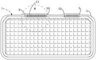
如图1至图6所示,为本发明一实施例所提供的触摸屏,该触摸屏包括:第一表面1和第二表面2。其中,第一表面1和第二表面2相背设置的;另外,第一表面1设有用于与电路板相接的第一绑定区11,第二表面覆盖2有第一绝缘保护层3;此外,第二表面2与第一绑定区11相对的区域设有第一辅助块4,第一辅助块4与第一绝缘保护层3相接触,通过第一绝缘保护层3与第一辅助块4的粘接可以防止第一绝缘保护层3翘起。另外,在本实施例中,第二表面2与第一绑定区11相对应的区域(在本发明中定义该区域为A区域)是指在垂直于第一表面1的方向上,第二表面2的投影与第一绑定区11的投影重合的区域。As shown in FIG. 1 to FIG. 6 , it is a touch screen provided by an embodiment of the present invention. The touch screen includes: a first surface 1 and a
在本发明提供的实施例中,第一辅助块4与第一绝缘保护层3之间的黏接强度大于第二表面2与第一绝缘保护层3之间的黏接强度。由于第一绝缘保护层3与第一辅助块4之间具有更好的黏接性能,故相比于现有设计而言(现有设计中,A区域未设置第一辅助块4,第一绝缘保护层3直接与第二表面2粘接),本实施例所提供的触摸屏,可以更好地解决第一绝缘保护层3位于A区域部分的边缘翘起的问题,从而可以有效减少因第一绝缘保护层3边缘翘起所导致的第一绝缘保护层3与第二表面2之间产生气泡或者第一绝缘保护层3从第二表面2上脱落等问题的出现,提高第一绝缘保护层3粘贴的良品率。In the embodiment provided by the present invention, the adhesive strength between the first auxiliary block 4 and the first insulating
如图3所示,在本发明提供的实施例中,第一辅助块4的个数为一,其中,第一辅助块4呈长条状,其长度与A区域的长度匹配,且第一辅助块4与第一绝缘保护层3相接触的表面为一平面,这样可以避免二者贴合处产生镂空缺陷,进一步降低第一绝缘保护层3边缘翘起的可能性。As shown in FIG. 3 , in the embodiment provided by the present invention, the number of the first auxiliary block 4 is one, wherein the first auxiliary block 4 is in the shape of a long strip, and its length matches the length of the A area, and the first auxiliary block 4 is in the shape of a long strip. The surface of the auxiliary block 4 in contact with the first insulating
如图5所示,在本发明提供的另一实施例中,第一辅助块4的为个数大于等于两个,这些第一辅助块4依次间隔设置,这样可以利用各第一辅助块4之间的间隙来排出第一绝艳保护层3与第二表面2之间的气泡,另外这些第一辅助块用于与第一绝缘保护层相接触的表面齐平,以便使各第一辅助块4均于第一绝缘保护层3相接触,避免第一绝缘保护层3翘起。As shown in FIG. 5 , in another embodiment provided by the present invention, the number of the first auxiliary blocks 4 is greater than or equal to two, and these first auxiliary blocks 4 are arranged at intervals in sequence, so that each first auxiliary block 4 can be used. The gap between the first bright
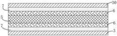
如图7所示,在本实施例中,触摸屏包括保护基板5、分别设置在基板5正面和背面的ITO导电层6、分别设置在ITO导电层6上的金属层7,即在本实施例中触摸屏为双ITO触摸屏,其中,基板5可以为PET板(PET为Polyethylene terephthalate的缩写,中文名称为:聚对苯二甲酸乙二酯)、COP板(COP为Cyclo Olefin Polymer的缩写,中文名称为:环烯烃聚合物)、玻璃板等透明基板,金属层7通常为用铜层。经曝光、显影、蚀刻等工艺后,会得到位于基板5正面的正面线路层,以及位于基板背面的背面线路层(图中未标注)。As shown in FIG. 7, in this embodiment, the touch screen includes a
其中,触摸屏的第一表面1包括正面线路层8远离基板5正面的表面,以及基板5正面不被正面线路层覆盖的部分,第二表面2包括背面线路层远离基板背面的表面,以及基板5背面不被背面线路线层覆盖的部分。另外,正面线路层8和背面线路层的结构设置相同,以下以正面线路层8为例进行说明,如图2所示,正面线路层8包括触控电极81、电极引线82,与电极引线电性相接的绑定块83,以及设置在电机引线外侧的地线84。电极引线82围绕在触摸屏的可视窗口周围;触控电极81设置在可视窗口内,用于产生电信号进而判断触控位置;绑定块83设置在第一绑定区11,用于与电路板的金手指(电极引脚)电性连接。The first surface 1 of the touch screen includes the surface of the
在本发明提供的实施例中,第一辅助4为TIO辅助块,ITO辅助块可以是由ITO导电层经过曝光、显影、蚀刻等工艺制成。即ITO辅助块和触控电极81可以是经同一生产工艺制成形成,这样可以减少触摸屏的生产工序,提高生产效率。可以理解的,在本发明提供的其他实施例中,第一辅助块4也可以采用其他材料制成,比如第一辅助块4可以是设置在基板5上的光学透明胶块等。In the embodiment provided by the present invention, the first auxiliary 4 is a TIO auxiliary block, and the ITO auxiliary block may be made of an ITO conductive layer through processes such as exposure, development, and etching. That is, the ITO auxiliary block and the touch electrodes 81 can be formed by the same production process, which can reduce the production process of the touch screen and improve the production efficiency. It can be understood that, in other embodiments provided by the present invention, the first auxiliary block 4 can also be made of other materials, for example, the first auxiliary block 4 can be an optically transparent glue block disposed on the
如图2所示,在实际产品中,地线84会在与第一绑定区11相对应的部分(在本发明中定义这部分地线为B部分)向内凹陷,以降低触摸屏在第一低绑定区11处的厚度,具体为:地线的内侧不变,外侧向内凹陷,使得该部分地线相对于其他部分的地线来说宽度较窄。故作为优选的,在本实施例中,ITO辅助块与地线相接触(即ITO辅助块与地线的B部分的外侧相接触),这样可以在一定程度上增大这部分地线的宽度,提高地线84的导电能力、抗冲击能力,以及抗腐蚀能力。可以理解的,当第一辅助块4为非导电材料制成时,第一辅助块也可以阻碍腐蚀液与地线接触,提高地线的防腐蚀能力。As shown in FIG. 2 , in an actual product, the
进一步的,在本实施例中,ITO辅助块与地线之间具有镂空区域111,这样可以有效防止蚀刻液在蚀刻地线时出现的扩散现象,从而提高地线的抗腐蚀能力。其中,如图2所示,ITO辅助块为一长条状结构,其两端分别与地线B部分的两端相接,这样可以形成一堤坝式结构,进一步提高地线84的导电能力、抗冲击能力,以及抗腐蚀能力。Further, in this embodiment, there is a
为了进一步降低第一绝缘保护层3位于A区域的边缘翘起的可能性,如图6所示,在本发明提供的实施例中,第一辅助块4与第一绝缘保护层3的边缘相接触,也即第一绝缘保护层3在A区域的边缘与第一辅助块4的边缘重合,或者第一绝缘保护层3在A区域的边缘的一部分或者全部位于第一辅助块4表面的中部。进一步的,在A区域内,第一绝缘保护层3的边缘与第二表面2的边缘齐平。即第一辅助块4的边缘也与第二表面2的边缘齐平,这样不仅可以提高第一绝缘保护层3的保护面积,还能进一步降低第一绝缘保护层3边缘翘起的可能性。In order to further reduce the possibility of the edge of the first insulating
在本发明提供的实施例中,第一绝缘保护层3为干膜,干膜贴设方便,且与第一辅助块4等具有良好的黏接性能,故第一绝缘保护层3采用干膜可以进一步提高触摸屏保护膜粘贴的良品率。In the embodiment provided by the present invention, the first insulating
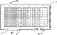
如图1所示,在本发明提供的实施例中,在基板两侧都设有线路层的触摸屏中,比如双ITO触摸屏,基板两侧的线路层都需要与电路板相接,第二表面2设有第二绑定区21(其中第二绑定区21与第一绑定区11错位设置,即在垂直于第一表面的方向上,第一绑定区11和第二绑定区21的投影不重合),第一表面1覆盖有第二绝缘保护层30,为了保证第二绝缘保护层30与第一表面1之间的贴合效果,在本发明提供的实施例中,第一表面1与第二绑定区21相对的区域设有第二辅助块40,其中,第二辅助块40与第二绝缘保护层30的特性与上述各实施例中第一辅助块4与第一绝缘保护层3的特性相同,本发明在此不做过多说明。As shown in FIG. 1, in the embodiment provided by the present invention, in a touch screen with circuit layers on both sides of the substrate, such as a dual ITO touch screen, the circuit layers on both sides of the substrate need to be connected to the circuit board, and the
在实际生产过程中,先在大片的基板上形成多个线路层,再在大片的基板上覆盖大片的绝缘保护层,得到能制作多个触摸屏的触控组件。然后采用刀模冲切作业,切断基板和绝缘保护层,将单个触摸屏从触控组件上分离下来。In the actual production process, a plurality of circuit layers are first formed on a large substrate, and then a large insulating protective layer is covered on the large substrate to obtain a touch component capable of producing multiple touch screens. Then a die-cutting operation is used to cut off the substrate and insulating protective layer, and separate the single touch screen from the touch assembly.
为了避免冲切时损坏触摸屏,切口位置距离线路层的外侧有一定距离,即线路层的外侧具有预留区,在该预留区内基板与绝缘保护层直接贴合,因此在该预留区域内,绝缘保护层与基板之间也会因为的附着力不够的原因而导致绝缘护层边缘的翘起。故为了进一步提高绝缘保护层的贴合效果,如图6所示,在本发明提供的实施例中,该预留区域的基板5上设有第三辅助块400,其中,第三辅助块400的特性与第一辅助块4的特性相同。In order to avoid damage to the touch screen during punching, the position of the incision is at a certain distance from the outside of the circuit layer, that is, there is a reserved area on the outside of the circuit layer. In the reserved area, the substrate and the insulating protective layer are directly attached. In addition, due to insufficient adhesion between the insulating protective layer and the substrate, the edge of the insulating protective layer will be lifted. Therefore, in order to further improve the bonding effect of the insulating protective layer, as shown in FIG. 6 , in the embodiment provided by the present invention, a third
本发明还提供了一种电子设备,该电子设备使用了上述任一实施例所述的触摸屏,其中,电子设备可以是智能手机、平板电脑等产品。The present invention also provides an electronic device, which uses the touch screen described in any of the above embodiments, wherein the electronic device may be a product such as a smart phone, a tablet computer, or the like.
以上所述实施例的各技术特征可以进行任意的组合,为使描述简洁,未对上述实施例中的各个技术特征所有可能的组合都进行描述,然而,只要这些技术特征的组合不存在矛盾,都应当认为是本说明书记载的范围。The technical features of the above-described embodiments can be combined arbitrarily. For the sake of brevity, all possible combinations of the technical features in the above-described embodiments are not described. However, as long as there is no contradiction between the combinations of these technical features, All should be regarded as the scope described in this specification.
以上所述实施例仅表达了本发明的几种实施方式,其描述较为具体和详细,但并不能因此而理解为对发明专利范围的限制。应当指出的是,对于本领域的普通技术人员来说,在不脱离本发明构思的前提下,还可以做出若干变形和改进,这些都属于本发明的保护范围。因此,本发明专利的保护范围应以所附权利要求为准。The above-mentioned embodiments only represent several embodiments of the present invention, and the descriptions thereof are specific and detailed, but should not be construed as a limitation on the scope of the invention patent. It should be pointed out that for those of ordinary skill in the art, without departing from the concept of the present invention, several modifications and improvements can also be made, which all belong to the protection scope of the present invention. Therefore, the protection scope of the patent of the present invention should be subject to the appended claims.
Claims (9)
Translated fromChinesePriority Applications (1)
| Application Number | Priority Date | Filing Date | Title |
|---|---|---|---|
| CN201811583990.0ACN111352516B (en) | 2018-12-24 | 2018-12-24 | Touch screen and electronic equipment |
Applications Claiming Priority (1)
| Application Number | Priority Date | Filing Date | Title |
|---|---|---|---|
| CN201811583990.0ACN111352516B (en) | 2018-12-24 | 2018-12-24 | Touch screen and electronic equipment |
Publications (2)
| Publication Number | Publication Date |
|---|---|
| CN111352516A CN111352516A (en) | 2020-06-30 |
| CN111352516Btrue CN111352516B (en) | 2022-08-19 |
Family
ID=71193911
Family Applications (1)
| Application Number | Title | Priority Date | Filing Date |
|---|---|---|---|
| CN201811583990.0AActiveCN111352516B (en) | 2018-12-24 | 2018-12-24 | Touch screen and electronic equipment |
Country Status (1)
| Country | Link |
|---|---|
| CN (1) | CN111352516B (en) |
Families Citing this family (1)
| Publication number | Priority date | Publication date | Assignee | Title |
|---|---|---|---|---|
| CN113157138B (en)* | 2021-05-11 | 2022-04-22 | 业成科技(成都)有限公司 | Touch module, manufacturing method thereof and electronic equipment |
Citations (7)
| Publication number | Priority date | Publication date | Assignee | Title |
|---|---|---|---|---|
| CN103828076A (en)* | 2011-08-01 | 2014-05-28 | 株式会社Steq | Semiconductor device and fabrication method for same |
| WO2014134895A1 (en)* | 2013-03-08 | 2014-09-12 | 南昌欧菲光科技有限公司 | Touch screen and manufacturing method therefor |
| CN204129717U (en)* | 2014-10-22 | 2015-01-28 | 深圳唯一科技股份有限公司 | A kind of insulation system of touch-screen |
| CN104375712A (en)* | 2014-12-10 | 2015-02-25 | 重庆墨希科技有限公司 | Production method of touchscreen binding area sliver paste protective structure |
| CN106354332A (en)* | 2016-09-30 | 2017-01-25 | 南昌欧菲显示科技有限公司 | Electronic device, touch display screen, touch assembly and touch conductive film |
| CN106604540A (en)* | 2015-10-19 | 2017-04-26 | 南昌欧菲光电技术有限公司 | Circuit board |
| CN207458015U (en)* | 2017-09-30 | 2018-06-05 | 南昌欧菲显示科技有限公司 | Flexible PCB, touch module and touch-screen |
Family Cites Families (3)
| Publication number | Priority date | Publication date | Assignee | Title |
|---|---|---|---|---|
| KR100295240B1 (en)* | 1997-04-24 | 2001-11-30 | 마찌다 가쯔히꼬 | Semiconductor device |
| US7411211B1 (en)* | 1999-07-22 | 2008-08-12 | Semiconductor Energy Laboratory Co., Ltd. | Contact structure and semiconductor device |
| TW201102702A (en)* | 2010-05-11 | 2011-01-16 | Mastouch Optoelectronics Technologies Co Ltd | Capacitive touch panel |
- 2018
- 2018-12-24CNCN201811583990.0Apatent/CN111352516B/enactiveActive
Patent Citations (7)
| Publication number | Priority date | Publication date | Assignee | Title |
|---|---|---|---|---|
| CN103828076A (en)* | 2011-08-01 | 2014-05-28 | 株式会社Steq | Semiconductor device and fabrication method for same |
| WO2014134895A1 (en)* | 2013-03-08 | 2014-09-12 | 南昌欧菲光科技有限公司 | Touch screen and manufacturing method therefor |
| CN204129717U (en)* | 2014-10-22 | 2015-01-28 | 深圳唯一科技股份有限公司 | A kind of insulation system of touch-screen |
| CN104375712A (en)* | 2014-12-10 | 2015-02-25 | 重庆墨希科技有限公司 | Production method of touchscreen binding area sliver paste protective structure |
| CN106604540A (en)* | 2015-10-19 | 2017-04-26 | 南昌欧菲光电技术有限公司 | Circuit board |
| CN106354332A (en)* | 2016-09-30 | 2017-01-25 | 南昌欧菲显示科技有限公司 | Electronic device, touch display screen, touch assembly and touch conductive film |
| CN207458015U (en)* | 2017-09-30 | 2018-06-05 | 南昌欧菲显示科技有限公司 | Flexible PCB, touch module and touch-screen |
Also Published As
| Publication number | Publication date |
|---|---|
| CN111352516A (en) | 2020-06-30 |
Similar Documents
| Publication | Publication Date | Title |
|---|---|---|
| US9760164B2 (en) | Touch panel and a manufacturing method thereof | |
| US20200210041A1 (en) | Touch display panel and bonding method thereof | |
| CN103226414B (en) | Touch screen and preparation method thereof | |
| CN103676386B (en) | A kind of display floater and display device | |
| US20180181224A1 (en) | Flexible touchscreen and flexible touch display | |
| WO2020000901A1 (en) | Conductive laminated structure, preparation method thereof, and touch control display device | |
| CN111755463A (en) | Display panel and display device | |
| CN107102461A (en) | A kind of preparation method of contact panel, display device and contact panel | |
| JP5914924B2 (en) | Transparent conductive film | |
| CN103941895B (en) | touch panel | |
| CN106648202A (en) | Electronic equipment, touch display screen, touch component and touch conducting film | |
| US9223357B2 (en) | Touch panel, manufacturing method thereof and touch display device | |
| JP2015524961A (en) | Transparent conductive film | |
| CN110970477B (en) | Organic light emitting display panel and display device | |
| CN104111747A (en) | Touch panel | |
| EP2527960A1 (en) | Touch-control pattern structure, manufacture method thereof and touch panel containing therein | |
| JP6195275B2 (en) | Input device and method for manufacturing input device | |
| CN111352516B (en) | Touch screen and electronic equipment | |
| CN104123050B (en) | Touch panel | |
| CN104407743A (en) | Touch control panel, manufacturing method of touch control panel and touch control display device | |
| CN105739732B (en) | Touch module and manufacturing method of touch module | |
| TWI550457B (en) | Touch panel and touch control module | |
| CN103226420B (en) | Manufacturing method of capacitive touch panel | |
| CN107833524A (en) | A kind of chip, flexible display panels and display device | |
| JP2014142785A (en) | Touch panel and touch panel manufacturing method |
Legal Events
| Date | Code | Title | Description |
|---|---|---|---|
| PB01 | Publication | ||
| PB01 | Publication | ||
| SE01 | Entry into force of request for substantive examination | ||
| SE01 | Entry into force of request for substantive examination | ||
| CB02 | Change of applicant information | Address after:330096 no.1404, Tianxiang North Avenue, Nanchang hi tech Industrial Development Zone, Nanchang City, Jiangxi Province Applicant after:Jiangxi Huiguang Microelectronics Co.,Ltd. Address before:330000 room 615, 28 Gaoxin 2nd Road, Nanchang hi tech Industrial Development Zone, Nanchang City, Jiangxi Province Applicant before:Nanchang Oufei Touch Technology Co.,Ltd. | |
| CB02 | Change of applicant information | ||
| TA01 | Transfer of patent application right | Effective date of registration:20220509 Address after:330029 room 1010, second floor, building 26, No. 8, zhouxindongyang Road, Xinqi, chuangcheng, traditional Chinese medicine, directly administered District, Ganjiang new area, Nanchang City, Jiangxi Province Applicant after:Jiangxi Zhuoxin Microelectronics Co.,Ltd. Address before:330096 no.1404, Tianxiang North Avenue, Nanchang hi tech Industrial Development Zone, Nanchang City, Jiangxi Province Applicant before:Jiangxi Huiguang Microelectronics Co.,Ltd. | |
| TA01 | Transfer of patent application right | ||
| GR01 | Patent grant | ||
| GR01 | Patent grant | ||
| PE01 | Entry into force of the registration of the contract for pledge of patent right | Denomination of invention:Touchscreen and electronic devices Granted publication date:20220819 Pledgee:Jiujiang Bank Co.,Ltd. Ganjiang New Area Guanglan Branch Pledgor:Jiangxi Zhuoxin Microelectronics Co.,Ltd. Registration number:Y2025980016776 | |
| PE01 | Entry into force of the registration of the contract for pledge of patent right |