CN111341817A - Pixel arrangement structure, display panel and display device - Google Patents
Pixel arrangement structure, display panel and display deviceDownload PDFInfo
- Publication number
- CN111341817A CN111341817ACN202010167886.4ACN202010167886ACN111341817ACN 111341817 ACN111341817 ACN 111341817ACN 202010167886 ACN202010167886 ACN 202010167886ACN 111341817 ACN111341817 ACN 111341817A
- Authority
- CN
- China
- Prior art keywords
- sub
- pixel
- virtual
- pixels
- distance
- Prior art date
- Legal status (The legal status is an assumption and is not a legal conclusion. Google has not performed a legal analysis and makes no representation as to the accuracy of the status listed.)
- Granted
Links
Images


Classifications
- H—ELECTRICITY
- H10—SEMICONDUCTOR DEVICES; ELECTRIC SOLID-STATE DEVICES NOT OTHERWISE PROVIDED FOR
- H10K—ORGANIC ELECTRIC SOLID-STATE DEVICES
- H10K59/00—Integrated devices, or assemblies of multiple devices, comprising at least one organic light-emitting element covered by group H10K50/00
- H10K59/30—Devices specially adapted for multicolour light emission
- H10K59/35—Devices specially adapted for multicolour light emission comprising red-green-blue [RGB] subpixels
- H10K59/353—Devices specially adapted for multicolour light emission comprising red-green-blue [RGB] subpixels characterised by the geometrical arrangement of the RGB subpixels
- H—ELECTRICITY
- H10—SEMICONDUCTOR DEVICES; ELECTRIC SOLID-STATE DEVICES NOT OTHERWISE PROVIDED FOR
- H10K—ORGANIC ELECTRIC SOLID-STATE DEVICES
- H10K59/00—Integrated devices, or assemblies of multiple devices, comprising at least one organic light-emitting element covered by group H10K50/00
- H10K59/30—Devices specially adapted for multicolour light emission
- H10K59/35—Devices specially adapted for multicolour light emission comprising red-green-blue [RGB] subpixels
- H10K59/352—Devices specially adapted for multicolour light emission comprising red-green-blue [RGB] subpixels the areas of the RGB subpixels being different
- H—ELECTRICITY
- H10—SEMICONDUCTOR DEVICES; ELECTRIC SOLID-STATE DEVICES NOT OTHERWISE PROVIDED FOR
- H10K—ORGANIC ELECTRIC SOLID-STATE DEVICES
- H10K59/00—Integrated devices, or assemblies of multiple devices, comprising at least one organic light-emitting element covered by group H10K50/00
- H10K59/60—OLEDs integrated with inorganic light-sensitive elements, e.g. with inorganic solar cells or inorganic photodiodes
- H10K59/65—OLEDs integrated with inorganic image sensors
- H—ELECTRICITY
- H10—SEMICONDUCTOR DEVICES; ELECTRIC SOLID-STATE DEVICES NOT OTHERWISE PROVIDED FOR
- H10K—ORGANIC ELECTRIC SOLID-STATE DEVICES
- H10K71/00—Manufacture or treatment specially adapted for the organic devices covered by this subclass
- H10K71/10—Deposition of organic active material
- H10K71/16—Deposition of organic active material using physical vapour deposition [PVD], e.g. vacuum deposition or sputtering
- H10K71/166—Deposition of organic active material using physical vapour deposition [PVD], e.g. vacuum deposition or sputtering using selective deposition, e.g. using a mask
Landscapes
- Electroluminescent Light Sources (AREA)
Abstract
Description
Translated fromChinese技术领域technical field
本发明涉及显示技术领域,特别是涉及一种像素排布结构、显示面板及显示装置。The present invention relates to the field of display technology, and in particular, to a pixel arrangement structure, a display panel and a display device.
背景技术Background technique
随着显示技术的不断发展,人们对于显示面板的分辨率的要求也越来越高。由于具有显示质量高等优点,高分辨率显示面板的应用范围也越来越广。通常,各子像素一般是通过有机材料利用蒸镀成膜技术透过精细掩膜板,在阵列基板上的相应的子像素位置形成有机电致发光结构。然而,当减小相邻子像素之间的距离以获得高开口率时,会增加掩膜板的制作难度,降低沉积可靠性。当增加子像素之间的距离以提高沉积可靠性时,会牺牲开口率。With the continuous development of display technology, people have higher and higher requirements for the resolution of the display panel. Due to the advantages of high display quality, the application range of high-resolution display panels is becoming wider and wider. Generally, each sub-pixel is generally made of organic material through a fine mask by using an evaporation film forming technique to form an organic electroluminescence structure at the corresponding sub-pixel position on the array substrate. However, when the distance between adjacent sub-pixels is reduced to obtain a high aperture ratio, the manufacturing difficulty of the mask plate is increased, and the deposition reliability is reduced. When increasing the distance between sub-pixels to improve deposition reliability, aperture ratio is sacrificed.
发明内容SUMMARY OF THE INVENTION
基于此,有必要提供一种像素排布结构、显示面板及显示装置,能够实现高像素密度的同时,降低掩膜板的制作难度。Based on this, it is necessary to provide a pixel arrangement structure, a display panel and a display device, which can achieve high pixel density and reduce the difficulty of manufacturing a mask.
根据本申请的一个方面,提供一种像素排布结构,包括:According to an aspect of the present application, a pixel arrangement structure is provided, comprising:
第一子像素,位于第一虚拟四边形的第一顶点位置处;a first subpixel, located at the position of the first vertex of the first virtual quadrilateral;
第二子像素,位于所述第一虚拟四边形的第二顶点位置处,所述第一顶点和所述第二顶点交替且间隔设置;及a second sub-pixel located at a position of a second vertex of the first virtual quadrangle, the first vertex and the second vertex are alternately and spaced apart; and
第三子像素,位于所述第一虚拟四边形内,且所述第三子像素的中心偏离第一虚拟四边形的中心;a third subpixel, located within the first virtual quadrilateral, and the center of the third subpixel is deviated from the center of the first virtual quadrilateral;
其中,沿行方向或列方向,所述第一虚拟四边形具有彼此相对的第一边和第二边,所述第一边的长度小于所述第二边的长度;Wherein, along the row direction or the column direction, the first virtual quadrilateral has a first side and a second side opposite to each other, and the length of the first side is smaller than the length of the second side;
在所述第一虚拟四边形中,位于所述第二边的所述第一子像素距所述第三子像素的距离,大于位于所述第一边的所述第一子像素距所述第三子像素的距离。In the first virtual quadrilateral, the distance between the first sub-pixel located on the second side and the third sub-pixel is greater than the distance between the first sub-pixel located on the first side and the third sub-pixel. The distance of three sub-pixels.
上述的像素排布结构,在工艺条件相同的情况下,采用这种子像素排布结构,可以使共享第二边的相邻的两个第一虚拟四边形中的第三子像素的间距相较于其他排布形式增大,扩大了相邻的像素开口之间可以利用的距离,有利于张网力F的传输,减少了Mask的变形,降低了精细金属掩膜板制作工艺和蒸镀工艺的难度。The above-mentioned pixel arrangement structure, under the same process conditions, using this sub-pixel arrangement structure can make the spacing of the third sub-pixels in the two adjacent first virtual quadrilaterals sharing the second side compared to The increase of other arrangement forms expands the usable distance between adjacent pixel openings, which is beneficial to the transmission of the tension force F, reduces the deformation of the Mask, and reduces the difficulty of the fine metal mask manufacturing process and the evaporation process.
在一实施例中,所述第一子像素的中心与所述第一顶点彼此重合;In one embodiment, the center of the first sub-pixel and the first vertex coincide with each other;
所述第二子像素的中心与所述第二顶点彼此重合。The center of the second sub-pixel and the second vertex coincide with each other.
在一实施例中,所述第一边与所述第二边彼此平行。In one embodiment, the first side and the second side are parallel to each other.
在一实施例中,在所述第一虚拟四边形中,一个所述第一子像素距相邻的任一第二子像素的距离,和另一个所述第一子像素距相邻的任一第二子像素的距离不相等。In one embodiment, in the first virtual quadrilateral, the distance between one of the first sub-pixels and any adjacent second sub-pixels, and the distance between the other first sub-pixels and any adjacent ones The distances of the second sub-pixels are not equal.
在一实施例中,在所述第一虚拟四边形中,相对的两个内角中的一个小于90°,另一个大于90°。In an embodiment, in the first virtual quadrilateral, one of the two opposite interior angles is less than 90°, and the other is greater than 90°.
在一实施例中,在所述第一虚拟四边形中,所述第三子像素的中心与任一所述第一子像素的中心之间的距离,不等于所述第三子像素的中心与任一所述第二子像素的中心之间的距离。In one embodiment, in the first virtual quadrilateral, the distance between the center of the third subpixel and the center of any one of the first subpixels is not equal to the distance between the center of the third subpixel and the center of any one of the first subpixels. The distance between the centers of any of the second sub-pixels.
在一实施例中,多个所述第一虚拟四边形以共享边的方式排布形成阵列。In one embodiment, a plurality of the first virtual quadrilaterals are arranged in a manner of sharing sides to form an array.
在一实施例中,在行方向或列方向,任意共享所述第一边或第二边的两个第一虚拟四边形为一组;在相邻行或列共享所述第二边或第一边的两个第一虚拟四边形为另一组;In an embodiment, in the row direction or the column direction, two first virtual quadrilaterals that arbitrarily share the first side or the second side are a group; in adjacent rows or columns, the second side or the first side is shared. The two first virtual quadrilaterals of the sides are another set;
两组中四个所述第一虚拟四边形共享一个所述第一顶点或所述第二顶点,两组所述第一虚拟四边形中的所述第三子像素的中心连线形成第二虚拟四边形;Four of the first virtual quadrilaterals in the two groups share one of the first vertex or the second vertex, and a line connecting the centers of the third sub-pixels in the two groups of the first virtual quadrilaterals forms a second virtual quadrilateral ;
所述第二虚拟四边形沿列方向或行方向具有彼此相对且长度不等的第三边和第四边。The second virtual quadrilateral has a third side and a fourth side which are opposite to each other and have different lengths in a column direction or a row direction.
在一实施例中,所述第三边与所述第四边彼此平行。In one embodiment, the third side and the fourth side are parallel to each other.
在一实施例中,所述第三子像素的形状为长方形或类长方形;In one embodiment, the shape of the third sub-pixel is a rectangle or a rectangle-like shape;
多个所述第三子像素的纵长方向相对所述行方向或列方向沿相同方向倾斜设置。The longitudinal directions of the plurality of third sub-pixels are inclined in the same direction with respect to the row direction or the column direction.
在一实施例中,沿行方向或列方向,任一第三子像素的虚拟边和与距离该第三子像素相邻且更靠近的一个第三子像素的虚拟边之间的最小距离为第一距离;In one embodiment, along the row direction or the column direction, the minimum distance between the virtual edge of any third sub-pixel and the virtual edge of a third sub-pixel that is adjacent and closer to the third sub-pixel is first distance;
且沿列方向或行方向,该第三子像素的虚拟边和与其相邻的第三子像素的虚拟边之间的最小距离为第二距离;And along the column direction or the row direction, the minimum distance between the virtual edge of the third subpixel and the virtual edge of the third subpixel adjacent to it is the second distance;
其中,所述第一距离小于所述第二距离。Wherein, the first distance is smaller than the second distance.
在一实施例中,任意共享所述第二边的两个所述第一虚拟四边形中的两个所述第三子像素共用一个掩膜板开口。In an embodiment, two of the third sub-pixels in the two first virtual quadrilaterals that arbitrarily share the second side share one mask opening.
在一实施例中,所述第二子像素的开口面积大于所述第一子像素的开口面积和所述第三子像素的开口面积。In one embodiment, the opening area of the second sub-pixel is larger than the opening area of the first sub-pixel and the opening area of the third sub-pixel.
根据本申请的另一方面,提供一种显示面板,包括如上述实施例所述的像素排布结构。According to another aspect of the present application, a display panel is provided, including the pixel arrangement structure described in the above embodiments.
根据本申请的又一方面,提供一种显示装置,包括如上述实施例所述的显示面板。According to yet another aspect of the present application, a display device is provided, including the display panel described in the above embodiments.
附图说明Description of drawings
图1为现有技术中的掩膜板的结构示意图;1 is a schematic structural diagram of a mask plate in the prior art;
图2为本申请一实施例中的显示面板的结构示意图;FIG. 2 is a schematic structural diagram of a display panel in an embodiment of the present application;
图3为蓝光、绿光和蓝光的光谱曲线图;Fig. 3 is the spectral curve diagram of blue light, green light and blue light;
图4为本申请一实施例中像素排布示意图;FIG. 4 is a schematic diagram of pixel arrangement in an embodiment of the present application;
图5为本申请另一实施例中的像素排布示意图;FIG. 5 is a schematic diagram of pixel arrangement in another embodiment of the present application;
图6为本申请又一实施例中的像素排布示意图;FIG. 6 is a schematic diagram of pixel arrangement in another embodiment of the present application;
图7为本申请再一实施例中的像素排布示意图。FIG. 7 is a schematic diagram of pixel arrangement in still another embodiment of the present application.
具体实施方式Detailed ways
为了便于理解本发明,下面将参照相关附图对本发明进行更全面的描述。附图中给出了本发明的较佳的实施例。但是,本发明可以以许多不同的形式来实现,并不限于本文所描述的实施例。相反地,提供这些实施例的目的是使对本发明的公开内容的理解更加透彻全面。In order to facilitate understanding of the present invention, the present invention will be described more fully hereinafter with reference to the related drawings. Preferred embodiments of the invention are shown in the accompanying drawings. However, the present invention may be embodied in many different forms and is not limited to the embodiments described herein. Rather, these embodiments are provided so that a thorough and complete understanding of the present disclosure is provided.
需要说明的是,当元件被称为“固定于”另一个元件,它可以直接在另一个元件上或者也可以存在居中的元件。当一个元件被认为是“连接”另一个元件,它可以是直接连接到另一个元件或者可能同时存在居中元件。本文所使用的术语“垂直的”、“水平的”、“左”、“右”以及类似的表述只是为了说明的目的。It should be noted that when an element is referred to as being "fixed to" another element, it can be directly on the other element or intervening elements may also be present. When an element is referred to as being "connected" to another element, it can be directly connected to the other element or intervening elements may also be present. The terms "vertical," "horizontal," "left," "right," and similar expressions are used herein for illustrative purposes only.
除非另有定义,本文所使用的所有的技术和科学术语与属于本发明的技术领域的技术人员通常理解的含义相同。本文中在本发明的说明书中所使用的术语只是为了描述具体的实施例的目的,不是旨在于限制本发明。本文所使用的术语“及/或”包括一个或多个相关的所列项目的任意的和所有的组合。Unless otherwise defined, all technical and scientific terms used herein have the same meaning as commonly understood by one of ordinary skill in the art to which this invention belongs. The terms used herein in the description of the present invention are for the purpose of describing specific embodiments only, and are not intended to limit the present invention. As used herein, the term "and/or" includes any and all combinations of one or more of the associated listed items.
目前的OLED显示面板的彩色化方法有许多种,现在较为成熟并大量量产的OLED彩色化技术是OLED蒸镀技术,具体是是利用蒸镀成膜技术透过高精细金属掩膜版(FineMetal Mask,FMM)在array(阵列)基板上相应的子像素位置形成有机发光元器件,所述高精细金属掩膜版通常简称为蒸镀掩膜版。制作高PPI(Pixel Per Inch,每英寸所拥有的像素数目)的OLED显示屏的技术重点在于精细性及机械稳定性好的FMM以及像素的排布方式。At present, there are many colorization methods for OLED display panels. Now the more mature and mass-produced OLED colorization technology is OLED evaporation technology. Mask, FMM) forms organic light-emitting components at corresponding sub-pixel positions on an array (array) substrate, and the high-precision metal mask is usually referred to as an evaporation mask for short. The technical focus of making an OLED display with high PPI (Pixel Per Inch, the number of pixels per inch) lies in the fineness and mechanical stability of the FMM and the arrangement of the pixels.
具体而言,FMM掩膜板应尽量少地发生翘曲、断裂等问题,避免造成蒸镀膜层晕开、偏移等影响蒸镀品质的缺陷。像素的排布方式是决定FMM是否容易发生翘曲和断裂的主要原因。即,子像素的排布方式较大程度上决定FMM的机械性能,FMM的机械性能较大程度上决定蒸镀的品质。例如,如图1所示,如果两个子像素的间距过小,这使得对应FMM的两个蒸镀开口之间的连接部分A具有断线的风险,且FMM和子像素区的对位空间会缩小,有可能产生缺色或混色的缺陷,若增加了连接部分的宽度,则需要缩小子像素的大小,影响OLED显示屏的开口率,不利于高分辨率的实现。因此,目前的OLED显示器件内,像素排布结构中的子像素之间的距离较大,导致同等分辨率的条件下,子像素的开口面积较小,从而需要增大驱动电流才能满足显示的亮度要求。但是,OLED在大驱动电流下工作容易导致器件老化,会出现大视角色偏的现象,且缩短了OLED显示器件的寿命。Specifically, the FMM mask should have as few problems as warpage and breakage as much as possible to avoid defects such as haloing and offset of the vapor-deposited film that affect the quality of the vapor-deposition. The way the pixels are arranged is the main factor that determines whether the FMM is prone to warping and breakage. That is, the arrangement of the sub-pixels determines the mechanical properties of the FMM to a large extent, and the mechanical properties of the FMM determine the quality of vapor deposition to a large extent. For example, as shown in FIG. 1, if the distance between the two sub-pixels is too small, the connection part A between the two evaporation openings corresponding to the FMM has the risk of disconnection, and the alignment space between the FMM and the sub-pixel area will be reduced , there may be defects of lack of color or color mixing. If the width of the connection part is increased, the size of the sub-pixel needs to be reduced, which affects the aperture ratio of the OLED display screen and is not conducive to the realization of high resolution. Therefore, in the current OLED display device, the distance between the sub-pixels in the pixel arrangement structure is relatively large, resulting in a small opening area of the sub-pixels under the condition of the same resolution, so it is necessary to increase the driving current to meet the display requirements. Brightness requirements. However, the operation of the OLED under a large driving current may easily lead to the aging of the device, a phenomenon of large viewing angle deviation will occur, and the life of the OLED display device will be shortened.
与此同时,为使终端设备实现更多的功能,屏下设置感光器件也越来越广泛,例如,在屏下设置指纹识别器件。其中,指纹图像获取的感光器件可以包括光学传感器,光学传感器中可以包括多个像素点,该多个像素点可以分别接收物体不同位置反射的光信号,并将入射光线转换成电信号,从而生成物体的图像。因此,像素点接收的光信号的进光量以及对比度均会影响生成物体的图像质量。如此,对显示面板的透光性也具有一定的要求,进一地为像素排布结构的设计增加了难度。At the same time, in order to enable the terminal device to achieve more functions, it is becoming more and more common to set photosensitive devices under the screen, for example, a fingerprint identification device is set under the screen. Wherein, the photosensitive device for fingerprint image acquisition may include an optical sensor, and the optical sensor may include a plurality of pixel points, and the plurality of pixel points can respectively receive light signals reflected from different positions of the object, and convert the incident light into electrical signals, thereby generating image of the object. Therefore, the amount of incoming light and the contrast of the light signal received by the pixels will affect the image quality of the generated object. In this way, the light transmittance of the display panel also has certain requirements, which further increases the difficulty in designing the pixel arrangement structure.
为解决上述问题,本发明提供了一种像素排布结构、显示面板及显示装置,能够较佳地改善上述问题。In order to solve the above problems, the present invention provides a pixel arrangement structure, a display panel and a display device, which can preferably improve the above problems.
图2示出了本申请一实施例中的显示面板的结构示意图;图3示出了各颜色光的光谱曲线图;图4示出了本申请一实施例中的像素排布示意图;图5示出了本申请另一实施例中的像素排布示意图。Fig. 2 shows a schematic structural diagram of a display panel in an embodiment of the present application; Fig. 3 shows a spectral curve diagram of each color light; Fig. 4 shows a schematic diagram of pixel arrangement in an embodiment of the present application; Fig. 5 A schematic diagram of pixel arrangement in another embodiment of the present application is shown.
参阅附图,本申请一实施例中的显示面板100,包括显示区域10和非显示区域20,显示区域10通过多个子像素来显示图像。具体到一些实施例中,显示区域10可以为矩形,非显示区域20环绕显示区域10设置,当然,显示区域10和非显示区域20的形状和布置包括但不限于上述的示例,例如,当显示面板100用于佩戴在用户上的可穿戴设备时,显示区域10可以具有像手表一样的圆形形状;当显示基板用于车辆上进行显示时,显示区域10及非显示区域20可采用例如圆形、多边形或其他形状。显示区域10设有发射不同颜色光的多个子像素,子像素表征为用于发射光的最小单元(例如,显示面板100的最小可寻址单元)。本申请的实施例中,像素排布结构包括发射不同颜色光的第一子像素12、第二子像素14及第三子像素16,第一子像素12、第二子像素14和第三子像素16可以分别为红色子像素、蓝色子像素和绿色子像素中的一种,构成一个呈现白光的像素。当然,在其他一些实施例中,第一子像素12、第二子像素14和第三子像素16还可以为红色、绿色和蓝色之外的其他颜色,在此不作限定。Referring to the drawings, a
应当理解的是,不同颜色光具有不同的波长,波长越高意味着光的能量越高,能量高的光容易引起有机发光材料的衰变,使得发射能量高的光子的子像素更容易衰减。如图3所示的光谱曲线图中,横轴为波长,单位为纳米,纵坐标为光强,其中,由于蓝光波长相较于红光波长和绿光波长短,因此,蓝光的能量更高,发射蓝光的有机发光材料更容易发生衰变,导致像素单元中发出的光容易偏红,造成白光色偏现象。且,每个子像素发射的光通过微腔效应在阳极和阴极之间重复反射和再反射,进行放大和相长干涉,光的亮度增加,色偏情况进一步被放大。作为一种较佳地实施方式,如图4所示,蓝色子像素(第二子像素14)的发光面积(像素开口面积)大于红色子像素(第一子像素12)和绿色子像素(第三子像素16)的发光面积,这样,可以一定程度降低因发射不同颜色光的有机发光材料衰减速率不同而造成的显示不良。需要指出,由于人眼对绿光比较敏感,在一些实施方式中,绿色子像素的发光面积可以小于红色子像素的发光面积,当然,在另一些实施方式中,绿色子像素的发光面积也可以与绿色子像素的发光面积相等,在此不作限定。It should be understood that light of different colors has different wavelengths. Higher wavelengths mean higher energy of light. Light with high energy easily causes the decay of organic light-emitting materials, making sub-pixels emitting photons with high energy easier to decay. As shown in the spectrum graph shown in Figure 3, the horizontal axis is wavelength, the unit is nanometer, and the vertical axis is light intensity. Among them, since the wavelength of blue light is shorter than that of red light and green light, the energy of blue light is higher, The organic light-emitting material that emits blue light is more prone to decay, causing the light emitted from the pixel unit to be prone to reddish, resulting in the phenomenon of white light color shifting. In addition, the light emitted by each sub-pixel is repeatedly reflected and re-reflected between the anode and the cathode through the microcavity effect to perform amplification and constructive interference, the brightness of the light is increased, and the color shift is further amplified. As a preferred embodiment, as shown in FIG. 4 , the light-emitting area (pixel opening area) of the blue sub-pixel (the second sub-pixel 14 ) is larger than that of the red sub-pixel (the first sub-pixel 12 ) and the green sub-pixel ( The light-emitting area of the third sub-pixel 16), in this way, the display failure caused by the different decay rates of organic light-emitting materials emitting light of different colors can be reduced to a certain extent. It should be pointed out that since the human eye is more sensitive to green light, in some embodiments, the light-emitting area of the green sub-pixel may be smaller than that of the red sub-pixel. Of course, in other embodiments, the light-emitting area of the green sub-pixel may also be It is equal to the light-emitting area of the green sub-pixel, which is not limited here.
本申请实施例提供的显示面板100,可以为有机发光显示面板100,子像素至少包括阳极和阴极,以及位于阳极和阴极之间的发光层,驱动电路向阳极和阴极之间施加电压,激发载流子迁移,作用于发光层,从而发射出光线。具体地,发光层至少包括空穴传输层、有机材料层及电子传输层,阳极用于为空穴传输层提供空穴或传输空穴的电极,阴极用于给有机材料层提供电子或传输电子。一些实施方式中,显示面板100还可以包括像素定义层,像素定义层界定出了多个像素开口,子像素的发光层设于像素开口中,以避免相邻的子像素之间发生串色或干扰。例如,如图4或图5所示的实施例中,第一子像素12、第二子像素14和第三子像素16的形状均为矩形,内侧矩形的边称为像素边,即像素定义层(PDL层)的像素开口的边界,外侧矩形的边称为子像素的虚拟边,所述虚拟边是指Mask(掩膜板)遮挡时的子像素的外边界。子像素之间的距离,即是指子像素之间相邻的像素边之间的最小距离,例如,如图4所示,第一子像素12a距第三子像素16的距离为两个子像素的像素边之间的最小距离。较佳地,各子像素的每一像素边与对应的虚拟边彼此平行且距对应的虚拟边的垂直距离相等。这样使得最终的子像素排列更为均匀和规则,从而可以有效提高子像素的发光层的制作精度和良率,并降低Mask张网时产生褶皱风险。可以理解,在其他一些实施例中,第一子像素12、第二子像素14和第三子像素16的形状还可以为其他,例如,四边形、六边形、八边形或具有圆倒角的圆角四边形、圆角六边形或圆角八边形,在此不作限定。The
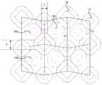
本申请的实施例中,第一子像素12位于第一虚拟四边形的第一顶点位置处,第二子像素14位于第一虚拟四边形的第二顶点位置处,第一顶点和第二顶点交替且间隔设置,即两个第一子像素12和两个第二子像素14可以分别位于第一虚拟四边形的相对的顶角处。第三子像素16位于第一虚拟四边形内,由两个第一子像素12和两个第二子像素14包围,这样,一方面,可以使各子像素排布更为紧凑,提高了各子像素的开口率;另一方面,可以将人眼敏感颜色的子像素放入第一虚拟四边形内,从而起到防止色偏的作用。例如,当通过红光、绿光和蓝光进行混色形成白光时,可以按照大致30%的红光、60%的绿光和10%的蓝光的比例进行混合。相较其他形式的排布方式,将第三子像素16设置为绿色子像素,可以使混色更均匀,且能够较佳地改善色偏。需要指出,子像素位于某一位置处,是指子像素所在的位置范围,只要保证子像素与该位置有重叠即可。例如,一些实施例中,子像素的中心可以与第一虚拟四边形的顶点不重合,即两者存在偏移;为了尽可能保证各子像素能够均匀分布,作为一种优选地实施例,第一子像素12可以具有与第一虚拟四边形的第一顶点重合的中心,第二子像素14可以具有与第一虚拟四边形的第二顶点重合的中心。子像素的中心可以是子像素图形的几何中心,也可以是子像素的发光颜色的中心,在此不作限定。In the embodiment of the present application, the
一些实施例中,该像素排布结构包括多个第一虚拟四边形,多个第一虚拟四边形以共享边的方式排布形成阵列,即相邻的两个像素组共用位于相邻的第一虚拟四边形侧边的第一子像素12和第二子像素14。例如,如图4所示的实施例中,在该阵列中,在第N行中的多个第一虚拟四边形与第N+1行中的多个第一虚拟四边形彼此啮合,第N行中的第一虚拟四边形的排布方式与第N+2行中的第一虚拟四边形的排布方式相同,其中,N≥1。这样,在显示时,任意相邻的两个第一子像素12和第二子像素14可以和与其相邻的第三子像素16组成一个发光像素,像素之间通过借色原理由低分辨率的物理分辨率实现高分辨率的显示效果。In some embodiments, the pixel arrangement structure includes a plurality of first virtual quadrilaterals, and the plurality of first virtual quadrilaterals are arranged in a manner of sharing sides to form an array, that is, two adjacent pixel groups share the adjacent first virtual quadrilaterals. The
本申请的实施例中,沿行方向或列方向,第一虚拟四边形具有彼此相对且长度不等的第一边a和第二边b,第一边a的长度小于第二边b的长度。如图4所示,具体到实施例中,第一虚拟四边形具有四个顶点,两个第一子像素12的中心与第一虚拟四边形相对的两个顶点重合,两个第二子像素14的中心与第一虚拟四边形另外两个相对的顶点重合,第一边a和第二边b均是以第一顶点和第二顶点为端点的两条边。其中,第一边a为沿行方向长度较短的侧边,第二边b为沿行方向长度较长的侧边,对应地,位于第一边a的第一子像素12和第二子像素14的间距较小,两者的虚拟边邻接,位于第二边b的第一子像素12和第二子像素14的间距较大,即两者的虚拟边间隔开来。容易理解,当第一虚拟四边形为正方形,第一子像素12距相邻的任意的第二子像素14的距离均相等,如此,可以使子像素的排布均匀,但受限于不同子像素的发光面积大小不同,以及受限于掩膜工艺,无法进一步有效提升开口率。而将第一虚拟四边形彼此相对的第一边a和第二边b设置为长度不等,则可以通过调整第一子像素12、第二子像素14和第三子像素16的位置,使子像素排布更加紧凑,在掩膜工艺的极限间距允许下,尽可能地降低了相邻子像素之间的间距,从而提高了子像素的开口率。作为一种可选地实施方式,第一边a和第二边b可以彼此平行设置,如图4和图5所示,在行方向,相邻的两个第一虚拟多边形以所述第一边a或第二边b对称设置。如此,可以使子像素的排布更为规整,提高了显示效果,且同色子像素可以排成一行或一列,降低了布线难度和掩膜板的制作难度。In the embodiment of the present application, along the row direction or the column direction, the first virtual quadrilateral has a first side a and a second side b that are opposite to each other and have unequal lengths, and the length of the first side a is smaller than the length of the second side b. As shown in FIG. 4 , specifically in the embodiment, the first virtual quadrilateral has four vertices, the centers of the two first sub-pixels 12 coincide with the two opposite vertices of the first virtual quadrilateral, and the two second sub-pixels 14 have four vertices. The center coincides with the other two opposite vertices of the first virtual quadrilateral, and both the first side a and the second side b are two sides whose endpoints are the first vertex and the second vertex. The first side a is the side with a shorter length along the row direction, and the second side b is a side with a longer length along the row direction. Correspondingly, the
本申请的实施例中,第三子像素16的中心偏离第一虚拟四边形的中心,且位于第二边b的第一子像素12距第三子像素16的距离,大于位于第一边a的第一子像素12距第三子像素16的距离。这样,在工艺条件相同的情况下,采用这种子像素排布结构,使共享第二边b的相邻的两个第一虚拟四边形中的第三子像素16的间距相较于其他排布形式增大,扩大了相邻的像素开口之间可以利用的距离,有利于张网力F的传输,减少了Mask的变形,降低了精细金属掩膜板制作工艺和蒸镀工艺的难度。具体地,如图4和图5所示,第三子像素16的中心偏离第一虚拟四边形的中心,第三子像素16距其中一个第一子像素12a的距离为c,该第三子像素16距另一个所述第一子像素12b的距离为d,其中,c>d。共享第二边b的两个第一虚拟四边形中的第三子像素16的虚拟边之间的间距h相较于其他排布形式增大,保证了第三子像素16的开口率的同时,降低了制作第三子像素16的掩膜板的难度。In the embodiment of the present application, the center of the
值得强调的是,屏下感光器件接收的光信号的进光量以及对比度均会影响生成物体的图像质量,采用其他像素排布结构的显示面板100,虽然可透光区域较多,使总体的透光面积无差异,但在特定区域内连续的透光区域的面积较小,无法满足屏下感光器件正常工作所需的光透过率。本申请的实施例中,在第一虚拟四边形中,两个第一子像素12距第三子像素16的距离不相等,可以增加连续的透光区域的面积,从而提高了显示面板100的透光率,为显示面板100的功能多样化提供了便利性。例如,如图4和图5所示的实施例中,相邻的两个第一虚拟四边形中的两个第三子像素16,与两个第一虚拟四边形共享的第一子像素12和第二子像素14的虚拟边之间可形成透光区域,多个相邻的第一虚拟四边形所对应的子像素的虚拟边之间的透光区域可连成一个大的透光区域,从而有效提高了显示面板100的光透过率。It is worth emphasizing that the amount of incoming light and the contrast of the light signal received by the photosensitive device under the screen will affect the image quality of the generated object. The
一些实施例中,在第一虚拟四边形中,第三子像素16的中心与任一第一子像素12的中心之间的距离不等于第三子像素16与任一第二子像素14的中心之间的距离。容易理解,增大衰减速率快的子像素的发光面积,可以改善色偏现象,但如果单纯增大子像素的发光面积,则子像素之间的距离会减小,如果不改变像素排布方式,则子像素的开口率会降低。将第三子像素16的中心与任一第一子像素12的中心之间的距离设置为不等于第三子像素16与任一第二子像素14的中心之间的距离,如此,可以保证第一子像素12、第二子像素14和第三子像素16之间尽可能紧密排列,在同等分辨率的条件下可以增大子像素的发光面积。例如,第三子像素16的中心与任一第一子像素12的中心之间的距离小于第三子像素16的中心与第二子像素14的中心之间的距离,使第一子像素12、第二子像素14和第三子像素16之间能够尽可能紧密排列,在同等分辨率的条件下可以增大第二子像素14的发光面积。作为可选地实施方式,第三子像素16的中心与两个第二子像素14的中心之间的距离可相等,也可不等,在此不作限定。In some embodiments, in the first virtual quadrilateral, the distance between the center of the
一些实施例中,在第一虚拟四边形中,一个第一子像素12距相邻的任一第二子像素14的距离,和另一个第一子像素12距相邻的任一第二子像素14的距离不相等。这样,可以使子像素的排布更为紧密,且有充足空间调节第三子像素的位置,满足两个第一子像素12a距第三子像素16的距离不同,从而增大共享第二边b的两个第三子像素之间的距离,有利于降低掩膜板的制作难度。例如,一些实施例中,在第一虚拟四边形中,第一子像素12a距相邻的两个第二子像素14之间的距离,小于第一子像素12b距相邻的两个第二子像素14之间的距离。如图4和图5所示,可以使第一子像素12a的虚拟边和其中一个相邻的第二子像素14的虚拟边邻接,和另一个相邻的第二子像素14的虚拟边间隔预设距离,最大限度的改善第一子像素12a和第二子像素14b之间的间距,有利于提高自像素的开口率。且同时,由于另一个第一子像素12b距相邻的两个第二子像素14较远,可以通过第三子像素16的位置,在尽量保证开口率的同时,使共享第二边b的两个第三子像素16间距增大,降低了掩膜板的制作难度。可以理解,在其他一些实施例中,第一子像素12a距相邻的两个第二子像素14的距离可以相等也可不等,第一子像素12b距相邻的两个第二子像素的距离可相等也可不等。也就是说,存在一种实施方式,在第一虚拟四边形中,任一相邻的第一子像素12与第二子像素14之间的距离均不相等,同样可以依据子像素的发光面积大小、掩膜板的制作难度合理设置距离,从而在保证开口率的同时,降低掩膜板的制作难度。一些实施例中,在第一虚拟四边形中,相对的两个内角中的一个小于90°,另一个大于90°。如图4和图5所示,在第一虚拟四边形中,第一边a平行于第二边b,对应两个第一子像素12位置所在的内角,一个小于90度,另一个大于90,对应两个第二子像素14位置所在的内角,一个同样小于90度,另一个大于90度。如此,在同等工艺条件下,使第一子像素12、第二子像素14和第三子像素16排布相较于其他方式(例如,相对的两个内角均小于90或大于90度)更紧密,可以有效提高子像素的开口率。当然,在另外一些实施例中,在第一虚拟四边形中,第一边a和第二边b亦可不平行,其中一对内角可以为90度,另外一对内角中一个内角小于90度,另一个内角大于90度,在此不作限定。值得强调的是,在第一虚拟四边形内,第一边a和第二边b若差异过大,则会造成第一虚拟四边形相对的内角差异过大,从而造成第一虚拟四边形过于松散,影响子像素的开口率。作为一种优选地实施方式,第一虚拟四边形内,第一边a的长度与第二边b的长度比值可以为0.5~0.95。具体到如图4所示的实施例中,第一边a的长度a小于第二边b的长度b,a:b的比值为0.5~0.95。这样,一方面防止第一虚拟四边形过于松散,另一方面在满足工艺极限的前提下,尽可能使子像素排布更为紧凑。In some embodiments, in the first virtual quadrilateral, the distance between one
需要说明的是,子像素之间的最小间距应当满足工艺极限间距,工艺极限间距与使用的制作工艺有关,例如,采用高精度金属掩膜板(FMM)配合刻蚀工艺形成子像素图形时,该最小间距约在16μm左右,采用激光或电铸工艺形成子像素图形时,该间距会更小。It should be noted that the minimum spacing between sub-pixels should meet the process limit spacing, which is related to the manufacturing process used. For example, when a high-precision metal mask (FMM) is used to form a sub-pixel pattern with an etching process, The minimum spacing is about 16 μm, and when the sub-pixel pattern is formed by a laser or electroforming process, the spacing will be smaller.
本申请的一些实施例中,在行方向或列方向,任意共享第一边a或第二边b的两个第一虚拟四边形为一组;在相邻行或列共享所述第二边b形或第一边a的两个第一虚拟四边形为另一组。两组中四个所述第一虚拟四边形共享一个第一顶点或第二顶点,两组所述第一虚拟四边形中的第三子像素16的中心连线形成第二虚拟四边形。例如,如图4和图5所示的实施例中,同一第一虚拟四边形中,第一边a平行于第二边b,在行方向上,两个第一虚拟四边形共享第一边a,在相邻行,两个第一虚拟四边形共享第二边b,四个第一虚拟四边形中的四个第三子像素16的中心连线形成第二虚拟四边形。其中,所述第二虚拟四边形沿列方向具有彼此相对且长度不等的第三边e和第四边f,采用如此设计,可以进一步地使第一子像素12、第二子像素14和第三子像素16排布更为紧凑,有利于提高子像素的开口面积,提高开口率。In some embodiments of the present application, in the row direction or the column direction, two first virtual quadrilaterals that arbitrarily share the first side a or the second side b are a group; the second side b is shared in adjacent rows or columns The two first virtual quadrilaterals of the shape or first side a are another group. The four first virtual quadrilaterals in the two groups share a first vertex or a second vertex, and a second virtual quadrilateral is formed by connecting the centers of the third sub-pixels 16 in the two groups of the first virtual quadrilaterals. For example, in the embodiments shown in FIGS. 4 and 5 , in the same first virtual quadrilateral, the first side a is parallel to the second side b, and in the row direction, the two first virtual quadrilaterals share the first side a, and the In adjacent rows, the two first virtual quadrilaterals share the second side b, and the center lines of the four third sub-pixels 16 in the four first virtual quadrilaterals form a second virtual quadrilateral. Wherein, the second virtual quadrilateral has a third side e and a fourth side f which are opposite to each other and have different lengths along the column direction. By adopting this design, the
作为一种实施方式,第二虚拟四边形中的第三边e和第四边f彼此平行,这样,可以使同一行或列中的第三子像素16的中心连线位于同一直线,进一步地降低了布线难度和掩膜板的制作难度。示例地,如图4和图5所示,第一虚拟四边形中,第一边a平行于第二边b,在第二虚拟四边形中,第三边e平行于第四边f,且第三边e和第四边f的延伸方向垂直于第一边a和第二边b的延伸方向。如此,进一步地使子像素的排布更为均匀和规则,有利于提高显示均匀性且降低了掩膜板的制作难度。As an implementation manner, the third side e and the fourth side f in the second virtual quadrilateral are parallel to each other, so that the center lines of the third sub-pixels 16 in the same row or column can be located on the same straight line, which further reduces the It reduces the difficulty of wiring and the difficulty of making the mask. 4 and 5, in the first virtual quadrilateral, the first side a is parallel to the second side b, in the second virtual quadrilateral, the third side e is parallel to the fourth side f, and the third side The extending directions of the side e and the fourth side f are perpendicular to the extending directions of the first side a and the second side b. In this way, the arrangement of the sub-pixels is further made more uniform and regular, which is beneficial to improve the display uniformity and reduce the manufacturing difficulty of the mask plate.
图6示出了本申请又一实施例中的像素排布示意图。FIG. 6 shows a schematic diagram of pixel arrangement in another embodiment of the present application.
参阅图6,本申请的一些实施例中,第三子像素16的形状为长方形或类长方形,多个第三子像素16的纵长方向相对行方向或列方向沿相同方向倾斜设置。应当理解的是,掩膜板受力通常沿行方向或列方向传递,例如,张网力F沿行方向传递,对应第三子像素16相对行方向或列方向倾斜设置的掩膜板的开口可以将受力在行方向和列方向分解,从而避免FMM张网力F集中造成的开口变形,降低了掩膜板的制作难度和张网难度。且掩膜板的开口倾斜设置,在同样长度和宽度的掩膜板中,可以设置更多的开口,降低了掩膜的制作成本。较佳地,第三子像素16的纵长方向相对行方向或列方向倾斜设置的角度为45°或135°。Referring to FIG. 6 , in some embodiments of the present application, the shape of the third sub-pixels 16 is a rectangle or a rectangle-like shape, and the longitudinal directions of the plurality of third sub-pixels 16 are inclined in the same direction relative to the row direction or the column direction. It should be understood that the force on the mask is usually transmitted in the row direction or the column direction, for example, the tension force F is transmitted in the row direction, and the opening of the mask plate corresponding to the
作为一种实施方式,沿行方向或列方向,任一第三子像素16的虚拟边和与距该第三子像素16相邻且更靠近的一个第三子像素16的虚拟边之间的最小距离为第一距离y。沿列方向或行方向,该第三子像素的虚拟边和与其相邻的第三子像素的虚拟边之间的最小距离为第二距离x,其中,y<x。也就是说,由于位于第二边b的第一子像素12距第三子像素16的距离,大于位于第一边a的第一子像素距第三子像素16的距离,则在行方向或列方向,存在任一第三子像素16与其相邻的两个第三子像素16之间的距离不相等。同时,为了兼顾子像素排布的紧密性且使第三子像素16的纵长方向相对行方向或列方向沿相同方向倾斜设置,则作为一种实施方式,可以设置为第一距离y小于第二距离x。例如,具体到一些实施例中,如图6所示,第三子像素16呈长方形,第三子像素16的对称轴的延伸方向相对行方向或列方向呈45°倾斜设置。如果第三子像素沿相同方向倾斜设置,且第三子像素16i的虚拟边与在行方向上相邻的第三子像素16j的虚拟边之间的距离y保持不变,且大于或等于其在列方向上相邻的第三子像素16k的虚拟边之间的距离x,则需要进一步压缩在列方向上相邻的第一子像素和第二子像素之间的间距。但如此会造成形成其他子像素掩膜板的制作难度增大,甚至是超过掩膜极限间距。因此,采用第三子像素16的虚拟边与位于同一行相邻的所述第三子像素16的虚拟边之间的距离y,小于与其位于同一列相邻的第三子像素16的虚拟边之间的距离x的设置,可以在尽可能使子像素排布更紧凑的前提下,使第三子像素的纵长方向沿相同方向倾斜设置。需要说明的是,类长方形是指,由于工艺限制或者为了掩膜板的制作便利,子像素的形状可能不是严格的平行四边形或长方形,而是大致为平行四边形或大致长方形,例如,具有圆角的圆角矩形或切角矩形。其中,圆角矩形是矩形的顶角被倒圆角形成的形状,切角矩形是矩形的顶角被切掉一个或多个所形成的形状。将子像素的形状设置为类平行四边形或类长方形可以更加灵活地调整子像素的开口率,并满足掩膜板在制作的限制条件。As an embodiment, along the row direction or the column direction, the distance between the virtual edge of any
图7示出了本申请再一实施例中的像素排布示意图。FIG. 7 shows a schematic diagram of pixel arrangement in still another embodiment of the present application.
参阅图7,本申请的一些实施例中,任意共享第二边b的两个第一虚拟四边形中的两个第三子像素16共用一个掩膜板开口。具体地,如图7所示,在列方向,共享第二边b的两个第一虚拟四边形中的第三子像素16以第二边b对称设置,且两个第三子像素16的中心之间的距离较小。如此,使共享第二边b的两个第一虚拟四边形中的第三子像素16可以共用一个Mask开口,在满足工艺条件下,可以制作更小尺寸的像素单元,从而增加显示面板100的PPI,进而提高了显示面板100的分辨率。Referring to FIG. 7 , in some embodiments of the present application, the two third sub-pixels 16 in the two first virtual quadrilaterals arbitrarily sharing the second side b share a mask opening. Specifically, as shown in FIG. 7 , in the column direction, the
基于同样的发明构思,本申请还提供一种掩膜板,用于制作本申请实施例提供的像素排布结构,该掩膜板包括多个开口区域,所述开口区域与第一子像素12、第二子像素14或第三子像素16的形状和位置相对应。Based on the same inventive concept, the present application also provides a mask for fabricating the pixel arrangement structure provided by the embodiment of the present application, the mask includes a plurality of opening areas, and the opening areas are connected to the
基于同样的发明构思,本申请还提供一种显示装置,该显示装置包括上述实施例中的显示面板100。Based on the same inventive concept, the present application also provides a display device, which includes the
具体地,该显示装置可以应用于手机终端、仿生电子、电子皮肤、可穿戴设备、车载设备、物联网设备及人工智能设备等领域。例如,上述显示装置可以为手机、平板、掌上电脑、ipod、智能手表等数码设备。Specifically, the display device can be applied to fields such as mobile phone terminals, bionic electronics, electronic skins, wearable devices, vehicle-mounted devices, Internet of Things devices, and artificial intelligence devices. For example, the above-mentioned display device may be a digital device such as a mobile phone, a tablet, a handheld computer, an ipod, and a smart watch.
在使用本文中描述的“包括”、“具有”、和“包含”的情况下,除非使用了明确的限定用语,例如“仅”、“由……组成”等,否则还可以添加另一部件。除非相反地提及,否则单数形式的术语可以包括复数形式,并不能理解为其数量为一个。Where "including", "having", and "comprising" are used as described herein, unless an explicit qualifying language is used, such as "only", "consisting of," etc., another component may also be added . Unless mentioned to the contrary, terms in the singular may include the plural and should not be construed as having a number of one.
应当理解,尽管本文可以使用术语“第一”、“第二”等来描述各种元件,但是这些元件不应受这些术语的限制。这些术语仅用于将一个元件和另一个元件区分开。例如,在不脱离本申请的范围的情况下,第一元件可以被称为第二元件,并且类似地,第二元件可以被称为第一元件。It will be understood that, although the terms "first," "second," etc. may be used herein to describe various elements, these elements should not be limited by these terms. These terms are only used to distinguish one element from another. For example, a first element could be termed a second element, and, similarly, a second element could be termed a first element, without departing from the scope of the present application.
以上所述实施例的各技术特征可以进行任意的组合,为使描述简洁,未对上述实施例中的各个技术特征所有可能的组合都进行描述,然而,只要这些技术特征的组合不存在矛盾,都应当认为是本说明书记载的范围。The technical features of the above-described embodiments can be combined arbitrarily. For the sake of brevity, all possible combinations of the technical features in the above-described embodiments are not described. However, as long as there is no contradiction between the combinations of these technical features, All should be regarded as the scope described in this specification.
以上所述实施例仅表达了本发明的几种实施方式,其描述较为具体和详细,但并不能因此而理解为对发明专利范围的限制。应当指出的是,对于本领域的普通技术人员来说,在不脱离本发明构思的前提下,还可以做出若干变形和改进,这些都属于本发明的保护范围。因此,本发明专利的保护范围应以所附权利要求为准。The above-mentioned embodiments only represent several embodiments of the present invention, and the descriptions thereof are specific and detailed, but should not be construed as a limitation on the scope of the invention patent. It should be pointed out that for those of ordinary skill in the art, without departing from the concept of the present invention, several modifications and improvements can also be made, which all belong to the protection scope of the present invention. Therefore, the protection scope of the patent of the present invention should be subject to the appended claims.
Claims (12)
Priority Applications (3)
| Application Number | Priority Date | Filing Date | Title |
|---|---|---|---|
| CN202010167886.4ACN111341817B (en) | 2020-03-11 | 2020-03-11 | Pixel arrangement structure, display panel and display device |
| PCT/CN2021/074460WO2021179837A1 (en) | 2020-03-11 | 2021-01-29 | Pixel arrangement structure, display panel, and display device |
| US17/697,696US12207517B2 (en) | 2020-03-11 | 2022-03-17 | Pixel arrangement structure, display panel, and display device |
Applications Claiming Priority (1)
| Application Number | Priority Date | Filing Date | Title |
|---|---|---|---|
| CN202010167886.4ACN111341817B (en) | 2020-03-11 | 2020-03-11 | Pixel arrangement structure, display panel and display device |
Publications (2)
| Publication Number | Publication Date |
|---|---|
| CN111341817Atrue CN111341817A (en) | 2020-06-26 |
| CN111341817B CN111341817B (en) | 2021-08-13 |
Family
ID=71187978
Family Applications (1)
| Application Number | Title | Priority Date | Filing Date |
|---|---|---|---|
| CN202010167886.4AActiveCN111341817B (en) | 2020-03-11 | 2020-03-11 | Pixel arrangement structure, display panel and display device |
Country Status (3)
| Country | Link |
|---|---|
| US (1) | US12207517B2 (en) |
| CN (1) | CN111341817B (en) |
| WO (1) | WO2021179837A1 (en) |
Cited By (33)
| Publication number | Priority date | Publication date | Assignee | Title |
|---|---|---|---|---|
| CN111785755A (en)* | 2020-07-03 | 2020-10-16 | 昆山国显光电有限公司 | Pixel structure and display panel |
| CN111816087A (en)* | 2020-07-17 | 2020-10-23 | 昆山国显光电有限公司 | Pixel structure and display panel |
| CN111864123A (en)* | 2020-07-16 | 2020-10-30 | 武汉华星光电半导体显示技术有限公司 | Display panel, mask set and display device |
| CN112038375A (en)* | 2020-09-02 | 2020-12-04 | 昆山国显光电有限公司 | Display panel and display device |
| CN112368840A (en)* | 2020-09-10 | 2021-02-12 | 京东方科技集团股份有限公司 | Pixel array and display device |
| CN112436032A (en)* | 2020-07-01 | 2021-03-02 | 昆山国显光电有限公司 | Display panel and display device |
| CN112436031A (en)* | 2020-07-01 | 2021-03-02 | 昆山国显光电有限公司 | Pixel arrangement structure, display panel and display device |
| CN112436030A (en)* | 2020-07-01 | 2021-03-02 | 昆山国显光电有限公司 | Pixel arrangement structure, display panel and display device |
| CN112436029A (en)* | 2020-07-01 | 2021-03-02 | 昆山国显光电有限公司 | Pixel arrangement structure, display panel and display device |
| CN112470287A (en)* | 2020-09-10 | 2021-03-09 | 京东方科技集团股份有限公司 | Display substrate and related device |
| CN113097277A (en)* | 2021-03-31 | 2021-07-09 | 武汉天马微电子有限公司 | Display panel and display device |
| CN113109993A (en)* | 2021-04-07 | 2021-07-13 | 深圳市华星光电半导体显示技术有限公司 | Typesetting method and typesetting system of display panel and electronic equipment |
| CN113327972A (en)* | 2021-07-01 | 2021-08-31 | 武汉天马微电子有限公司 | Display panel, preparation method and display device |
| WO2021179859A1 (en)* | 2020-03-11 | 2021-09-16 | 昆山国显光电有限公司 | Display panel and display device |
| WO2021179837A1 (en)* | 2020-03-11 | 2021-09-16 | 昆山国显光电有限公司 | Pixel arrangement structure, display panel, and display device |
| CN113471266A (en)* | 2021-06-30 | 2021-10-01 | 昆山国显光电有限公司 | Pixel arrangement structure, mask assembly and display panel |
| CN113488521A (en)* | 2021-07-01 | 2021-10-08 | 武汉天马微电子有限公司 | Display panel, display device and evaporation device |
| CN113964171A (en)* | 2021-11-22 | 2022-01-21 | 合肥维信诺科技有限公司 | Pixel arrangement structure, mask assembly and display panel |
| WO2022052011A1 (en)* | 2020-09-10 | 2022-03-17 | 京东方科技集团股份有限公司 | Display substrate, display device, and high-precision metal mask |
| WO2022052194A1 (en)* | 2020-09-10 | 2022-03-17 | 京东方科技集团股份有限公司 | Display substrate and related device |
| WO2022052390A1 (en)* | 2020-09-10 | 2022-03-17 | 京东方科技集团股份有限公司 | Pixel array and display device |
| WO2022052192A1 (en)* | 2020-09-10 | 2022-03-17 | 京东方科技集团股份有限公司 | Pixel array and display device |
| WO2022141628A1 (en)* | 2021-01-04 | 2022-07-07 | 京东方科技集团股份有限公司 | Display substrate and related device |
| WO2022194215A1 (en)* | 2021-03-16 | 2022-09-22 | 京东方科技集团股份有限公司 | Array substrate and display device |
| WO2023044974A1 (en)* | 2021-09-26 | 2023-03-30 | 武汉华星光电半导体显示技术有限公司 | Display panel |
| US20230143544A1 (en)* | 2020-11-30 | 2023-05-11 | Chengdu Boe Optoelectronics Technology Co., Ltd. | Display substrate, display device and high-precision metal mask |
| EP4177954A4 (en)* | 2020-07-01 | 2023-06-28 | Kunshan Go-Visionox Opto-Electronics Co., Ltd. | Pixel arrangement structure, display panel, and display device |
| JP2024501566A (en)* | 2021-06-17 | 2024-01-12 | 合肥維信諾科技有限公司 | Pixel array structure, mask assembly, and display panel |
| US11985841B2 (en) | 2020-12-07 | 2024-05-14 | Oti Lumionics Inc. | Patterning a conductive deposited layer using a nucleation inhibiting coating and an underlying metallic coating |
| US12113279B2 (en) | 2020-09-22 | 2024-10-08 | Oti Lumionics Inc. | Device incorporating an IR signal transmissive region |
| WO2025025101A1 (en)* | 2023-07-31 | 2025-02-06 | 京东方科技集团股份有限公司 | Pixel arrangement structure and display device |
| US12302730B2 (en) | 2020-09-29 | 2025-05-13 | Chengdu Boe Optoelectronics Technology Co., Ltd. | Pixel array and display device |
| US12433127B2 (en) | 2020-09-10 | 2025-09-30 | Chengdu Boe Optoelectronics Technology Co., Ltd. | Display substrate, display device and high-precision metal mask |
Families Citing this family (3)
| Publication number | Priority date | Publication date | Assignee | Title |
|---|---|---|---|---|
| CN114342068A (en) | 2019-08-09 | 2022-04-12 | Oti照明公司 | Optoelectronic device containing auxiliary electrodes and partitions |
| CN111509023B (en)* | 2020-05-06 | 2022-05-20 | 京东方科技集团股份有限公司 | Display panel and display device |
| US11974482B2 (en)* | 2020-11-30 | 2024-04-30 | Chengdu Boe Optoelectronics Technology Co., Ltd. | Display substrate and related devices |
Citations (4)
| Publication number | Priority date | Publication date | Assignee | Title |
|---|---|---|---|---|
| CN109860237A (en)* | 2018-12-13 | 2019-06-07 | 昆山国显光电有限公司 | Pixel arrangement structure, display panel and display device |
| CN110137206A (en)* | 2018-02-09 | 2019-08-16 | 京东方科技集团股份有限公司 | A kind of pixel arrangement structure and relevant apparatus |
| CN110137207A (en)* | 2018-02-09 | 2019-08-16 | 京东方科技集团股份有限公司 | A kind of pixel arrangement structure and relevant apparatus |
| US20200043990A1 (en)* | 2016-02-18 | 2020-02-06 | Chengdu Boe Optoelectronics Technology Co., Ltd. | Pixel arrangement structure, display substrate, display apparatus and method of fabrication thereof |
Family Cites Families (14)
| Publication number | Priority date | Publication date | Assignee | Title |
|---|---|---|---|---|
| TWI381742B (en)* | 2005-10-13 | 2013-01-01 | Seiko Epson Corp | Image display device, electronic apparatus, and pixel location determining method |
| KR101615332B1 (en) | 2012-03-06 | 2016-04-26 | 삼성디스플레이 주식회사 | Pixel arrangement structure for organic light emitting display device |
| WO2015062110A1 (en) | 2013-11-04 | 2015-05-07 | Shenzhen Yunyinggu Technology Co., Ltd. | Subpixel arrangements of displays and method for rendering the same |
| CN104050889B (en)* | 2014-05-30 | 2015-04-29 | 京东方科技集团股份有限公司 | Display device and drive method |
| TWI585968B (en)* | 2016-03-22 | 2017-06-01 | 群創光電股份有限公司 | Display device |
| CN107887404B (en) | 2016-09-29 | 2020-04-07 | 昆山国显光电有限公司 | AMOLED pixel structure and display device |
| CN106960863B (en)* | 2017-03-15 | 2019-06-14 | 上海天马有机发光显示技术有限公司 | The preparation method of display pixel arrangement, display panel and display panel |
| KR102520710B1 (en)* | 2017-09-05 | 2023-04-12 | 삼성디스플레이 주식회사 | Display device and method of manufacturing the same |
| CN207781594U (en)* | 2018-01-31 | 2018-08-28 | 昆山国显光电有限公司 | A kind of dot structure and display panel |
| CN109904200A (en) | 2019-02-27 | 2019-06-18 | 昆山国显光电有限公司 | Pixel arrangement structure, display panel and display device |
| CN110277436A (en)* | 2019-06-28 | 2019-09-24 | 云谷(固安)科技有限公司 | Pixel arrangement structure and display panel |
| CN111341815B (en)* | 2020-03-11 | 2021-08-13 | 昆山国显光电有限公司 | Pixel arrangement structure, display panel and display device |
| CN111341817B (en)* | 2020-03-11 | 2021-08-13 | 昆山国显光电有限公司 | Pixel arrangement structure, display panel and display device |
| KR20230010812A (en)* | 2020-07-01 | 2023-01-19 | 쿤산 고-비젼녹스 옵토-일렉트로닉스 씨오., 엘티디. | Pixel array structure, display panel and display device |
- 2020
- 2020-03-11CNCN202010167886.4Apatent/CN111341817B/enactiveActive
- 2021
- 2021-01-29WOPCT/CN2021/074460patent/WO2021179837A1/ennot_activeCeased
- 2022
- 2022-03-17USUS17/697,696patent/US12207517B2/enactiveActive
Patent Citations (4)
| Publication number | Priority date | Publication date | Assignee | Title |
|---|---|---|---|---|
| US20200043990A1 (en)* | 2016-02-18 | 2020-02-06 | Chengdu Boe Optoelectronics Technology Co., Ltd. | Pixel arrangement structure, display substrate, display apparatus and method of fabrication thereof |
| CN110137206A (en)* | 2018-02-09 | 2019-08-16 | 京东方科技集团股份有限公司 | A kind of pixel arrangement structure and relevant apparatus |
| CN110137207A (en)* | 2018-02-09 | 2019-08-16 | 京东方科技集团股份有限公司 | A kind of pixel arrangement structure and relevant apparatus |
| CN109860237A (en)* | 2018-12-13 | 2019-06-07 | 昆山国显光电有限公司 | Pixel arrangement structure, display panel and display device |
Cited By (72)
| Publication number | Priority date | Publication date | Assignee | Title |
|---|---|---|---|---|
| WO2021179859A1 (en)* | 2020-03-11 | 2021-09-16 | 昆山国显光电有限公司 | Display panel and display device |
| US12207517B2 (en) | 2020-03-11 | 2025-01-21 | Kunshan Go-Visionox Opto-Electronics Co., Ltd. | Pixel arrangement structure, display panel, and display device |
| WO2021179837A1 (en)* | 2020-03-11 | 2021-09-16 | 昆山国显光电有限公司 | Pixel arrangement structure, display panel, and display device |
| CN112436031B (en)* | 2020-07-01 | 2022-10-21 | 昆山国显光电有限公司 | Pixel arrangement structure, display panel and display device |
| WO2022001311A1 (en)* | 2020-07-01 | 2022-01-06 | 昆山国显光电有限公司 | Display panel and display device |
| CN112436032A (en)* | 2020-07-01 | 2021-03-02 | 昆山国显光电有限公司 | Display panel and display device |
| CN112436031A (en)* | 2020-07-01 | 2021-03-02 | 昆山国显光电有限公司 | Pixel arrangement structure, display panel and display device |
| CN112436030A (en)* | 2020-07-01 | 2021-03-02 | 昆山国显光电有限公司 | Pixel arrangement structure, display panel and display device |
| CN112436029A (en)* | 2020-07-01 | 2021-03-02 | 昆山国显光电有限公司 | Pixel arrangement structure, display panel and display device |
| JP2023532055A (en)* | 2020-07-01 | 2023-07-26 | クンシャン ゴー-ビシオノクス オプト-エレクトロニクス カンパニー リミテッド | Pixel array structure, display panel and display device |
| EP4203655A1 (en)* | 2020-07-01 | 2023-06-28 | Kunshan Go-Visionox Opto-Electronics Co., Ltd. | Pixel arrangement structure, display panel, and display device |
| EP4177954A4 (en)* | 2020-07-01 | 2023-06-28 | Kunshan Go-Visionox Opto-Electronics Co., Ltd. | Pixel arrangement structure, display panel, and display device |
| US12329010B1 (en) | 2020-07-01 | 2025-06-10 | Kunshan Go-Visionox Opto-Electronics Co., Ltd. | Display panels and display devices |
| JP7574340B2 (en) | 2020-07-01 | 2024-10-28 | クンシャン ゴー-ビシオノクス オプト-エレクトロニクス カンパニー リミテッド | PIXEL ARRAY STRUCTURE, DISPLAY PANEL AND DISPLAY DEVICE |
| JP7574341B2 (en) | 2020-07-01 | 2024-10-28 | クンシャン ゴー-ビシオノクス オプト-エレクトロニクス カンパニー リミテッド | PIXEL ARRAY STRUCTURE, DISPLAY PANEL AND DISPLAY DEVICE |
| CN112436032B (en)* | 2020-07-01 | 2022-10-18 | 昆山国显光电有限公司 | Display panel and display device |
| CN112436030B (en)* | 2020-07-01 | 2022-10-18 | 昆山国显光电有限公司 | Pixel arrangement structure, display panel and display device |
| JP7634026B2 (en) | 2020-07-01 | 2025-02-20 | クンシャン ゴー-ビシオノクス オプト-エレクトロニクス カンパニー リミテッド | PIXEL ARRAY STRUCTURE, DISPLAY PANEL AND DISPLAY DEVICE |
| CN112436029B (en)* | 2020-07-01 | 2022-10-18 | 昆山国显光电有限公司 | Pixel arrangement structure, display panel and display device |
| TWI763475B (en)* | 2020-07-01 | 2022-05-01 | 大陸商昆山國顯光電有限公司 | Display panel |
| CN111785755B (en)* | 2020-07-03 | 2022-10-25 | 昆山国显光电有限公司 | Pixel structure and display panel |
| CN111785755A (en)* | 2020-07-03 | 2020-10-16 | 昆山国显光电有限公司 | Pixel structure and display panel |
| CN111864123A (en)* | 2020-07-16 | 2020-10-30 | 武汉华星光电半导体显示技术有限公司 | Display panel, mask set and display device |
| CN111864123B (en)* | 2020-07-16 | 2021-09-24 | 武汉华星光电半导体显示技术有限公司 | Display panel, mask set and display device |
| CN111816087A (en)* | 2020-07-17 | 2020-10-23 | 昆山国显光电有限公司 | Pixel structure and display panel |
| CN112038375A (en)* | 2020-09-02 | 2020-12-04 | 昆山国显光电有限公司 | Display panel and display device |
| WO2022048223A1 (en)* | 2020-09-02 | 2022-03-10 | 昆山国显光电有限公司 | Display panel and display device |
| WO2022052010A1 (en)* | 2020-09-10 | 2022-03-17 | 京东方科技集团股份有限公司 | Display substrate and related apparatus |
| JP2023501031A (en)* | 2020-09-10 | 2023-01-18 | 京東方科技集團股▲ふん▼有限公司 | pixel array and display |
| EP4213212A4 (en)* | 2020-09-10 | 2025-01-15 | BOE Technology Group Co., Ltd. | PIXEL MATRIX AND DISPLAY DEVICE |
| CN114730800A (en)* | 2020-09-10 | 2022-07-08 | 京东方科技集团股份有限公司 | Pixel array and display device |
| US12150361B2 (en) | 2020-09-10 | 2024-11-19 | Chengdu Boe Optoelectronics Technology Co., Ltd. | Pixel array and display device |
| US12150360B2 (en) | 2020-09-10 | 2024-11-19 | Chengdu Boe Optoelectronics Technology Co., Ltd. | Pixel array and display device |
| WO2022052834A1 (en)* | 2020-09-10 | 2022-03-17 | 京东方科技集团股份有限公司 | Display substrate and display device |
| US12238998B2 (en) | 2020-09-10 | 2025-02-25 | Boe Technology Group Co., Ltd. | Pixel array with pixel groups forming trapezoids |
| WO2022052390A1 (en)* | 2020-09-10 | 2022-03-17 | 京东方科技集团股份有限公司 | Pixel array and display device |
| WO2022052194A1 (en)* | 2020-09-10 | 2022-03-17 | 京东方科技集团股份有限公司 | Display substrate and related device |
| WO2022052011A1 (en)* | 2020-09-10 | 2022-03-17 | 京东方科技集团股份有限公司 | Display substrate, display device, and high-precision metal mask |
| CN112368840A (en)* | 2020-09-10 | 2021-02-12 | 京东方科技集团股份有限公司 | Pixel array and display device |
| US11812648B2 (en) | 2020-09-10 | 2023-11-07 | Chengdu Boe Optoelectronics Technology Co., Ltd. | Pixel array and display device |
| WO2022052193A1 (en)* | 2020-09-10 | 2022-03-17 | 京东方科技集团股份有限公司 | Display substrate, display device, and high-precision metal mask |
| WO2022052192A1 (en)* | 2020-09-10 | 2022-03-17 | 京东方科技集团股份有限公司 | Pixel array and display device |
| CN114730800B (en)* | 2020-09-10 | 2023-12-22 | 京东方科技集团股份有限公司 | Pixel array and display device |
| US12433124B2 (en) | 2020-09-10 | 2025-09-30 | Chengdu Boe Optoelectronics Technology Co., Ltd. | Display substrate and display device |
| US12433127B2 (en) | 2020-09-10 | 2025-09-30 | Chengdu Boe Optoelectronics Technology Co., Ltd. | Display substrate, display device and high-precision metal mask |
| AU2020450961B2 (en)* | 2020-09-10 | 2023-07-06 | Boe Technology Group Co., Ltd. | Pixel array and display device |
| CN112470287A (en)* | 2020-09-10 | 2021-03-09 | 京东方科技集团股份有限公司 | Display substrate and related device |
| CN112470287B (en)* | 2020-09-10 | 2023-08-22 | 京东方科技集团股份有限公司 | Display substrate and related device |
| JP7342157B2 (en) | 2020-09-10 | 2023-09-11 | 京東方科技集團股▲ふん▼有限公司 | Pixel array and display device |
| US12113279B2 (en) | 2020-09-22 | 2024-10-08 | Oti Lumionics Inc. | Device incorporating an IR signal transmissive region |
| US12302730B2 (en) | 2020-09-29 | 2025-05-13 | Chengdu Boe Optoelectronics Technology Co., Ltd. | Pixel array and display device |
| US20230143544A1 (en)* | 2020-11-30 | 2023-05-11 | Chengdu Boe Optoelectronics Technology Co., Ltd. | Display substrate, display device and high-precision metal mask |
| US12156451B2 (en)* | 2020-11-30 | 2024-11-26 | Chengdu Boe Optoelectronics Technology Co., Ltd. | Display substrate, display device and high-precision metal mask |
| US11985841B2 (en) | 2020-12-07 | 2024-05-14 | Oti Lumionics Inc. | Patterning a conductive deposited layer using a nucleation inhibiting coating and an underlying metallic coating |
| US12382811B2 (en) | 2021-01-04 | 2025-08-05 | Chengdu Boe Optoelectronics Technology Co., Ltd. | Display substrate and related device |
| WO2022141628A1 (en)* | 2021-01-04 | 2022-07-07 | 京东方科技集团股份有限公司 | Display substrate and related device |
| CN115669276A (en)* | 2021-01-04 | 2023-01-31 | 京东方科技集团股份有限公司 | Display substrate and related device |
| WO2022194215A1 (en)* | 2021-03-16 | 2022-09-22 | 京东方科技集团股份有限公司 | Array substrate and display device |
| WO2022193414A1 (en)* | 2021-03-16 | 2022-09-22 | 京东方科技集团股份有限公司 | Array substrate and display apparatus |
| US12426442B2 (en) | 2021-03-16 | 2025-09-23 | Chengdu Boe Optoelectronics Technology Co., Ltd. | Array substrate and display device |
| CN113097277A (en)* | 2021-03-31 | 2021-07-09 | 武汉天马微电子有限公司 | Display panel and display device |
| CN113109993B (en)* | 2021-04-07 | 2023-06-02 | 深圳市华星光电半导体显示技术有限公司 | Typesetting method and typesetting system of display panel and electronic equipment |
| CN113109993A (en)* | 2021-04-07 | 2021-07-13 | 深圳市华星光电半导体显示技术有限公司 | Typesetting method and typesetting system of display panel and electronic equipment |
| JP7519550B2 (en) | 2021-06-17 | 2024-07-19 | 合肥維信諾科技有限公司 | PIXEL ARRAY STRUCTURE, MASK ASSEMBLY, AND DISPLAY PANEL |
| JP2024501566A (en)* | 2021-06-17 | 2024-01-12 | 合肥維信諾科技有限公司 | Pixel array structure, mask assembly, and display panel |
| CN113471266A (en)* | 2021-06-30 | 2021-10-01 | 昆山国显光电有限公司 | Pixel arrangement structure, mask assembly and display panel |
| CN113488521A (en)* | 2021-07-01 | 2021-10-08 | 武汉天马微电子有限公司 | Display panel, display device and evaporation device |
| CN113327972A (en)* | 2021-07-01 | 2021-08-31 | 武汉天马微电子有限公司 | Display panel, preparation method and display device |
| WO2023044974A1 (en)* | 2021-09-26 | 2023-03-30 | 武汉华星光电半导体显示技术有限公司 | Display panel |
| CN113964171A (en)* | 2021-11-22 | 2022-01-21 | 合肥维信诺科技有限公司 | Pixel arrangement structure, mask assembly and display panel |
| CN113964171B (en)* | 2021-11-22 | 2024-11-29 | 合肥维信诺科技有限公司 | Pixel arrangement structure, mask assembly and display panel |
| WO2025025101A1 (en)* | 2023-07-31 | 2025-02-06 | 京东方科技集团股份有限公司 | Pixel arrangement structure and display device |
Also Published As
| Publication number | Publication date |
|---|---|
| US20220208891A1 (en) | 2022-06-30 |
| CN111341817B (en) | 2021-08-13 |
| US12207517B2 (en) | 2025-01-21 |
| WO2021179837A1 (en) | 2021-09-16 |
Similar Documents
| Publication | Publication Date | Title |
|---|---|---|
| CN111341817A (en) | Pixel arrangement structure, display panel and display device | |
| CN111341815B (en) | Pixel arrangement structure, display panel and display device | |
| TWI763475B (en) | Display panel | |
| CN112436031B (en) | Pixel arrangement structure, display panel and display device | |
| CN110323259B (en) | Pixel structure, mask plate and display panel | |
| CN112436029B (en) | Pixel arrangement structure, display panel and display device | |
| US11568794B2 (en) | Pixel arrangement structure, metal mask, and display device | |
| US10720481B2 (en) | Pixel arrangement structure, organic light-emitting diode display panel, fine metal mask, and display device | |
| TWI780694B (en) | Pixel arrangement structure, display panel and display device | |
| TWI779689B (en) | Display panel and display device | |
| WO2020020337A1 (en) | Sub-pixel arrangement structure, masking apparatus, display panel and display device | |
| CN120152559A (en) | Pixel arrangement structure, display substrate and display device | |
| CN113327973A (en) | Display panel and display device | |
| CN112436030A (en) | Pixel arrangement structure, display panel and display device | |
| KR102841037B1 (en) | Pixel array structure, display panel and display device | |
| CN215418186U (en) | Display panel and display device |
Legal Events
| Date | Code | Title | Description |
|---|---|---|---|
| PB01 | Publication | ||
| PB01 | Publication | ||
| SE01 | Entry into force of request for substantive examination | ||
| SE01 | Entry into force of request for substantive examination | ||
| GR01 | Patent grant | ||
| GR01 | Patent grant |