CN111338314A - Semiconductor device, electronic control unit, verification method for electronic control unit, and manufacturing method for electronic control unit - Google Patents
Semiconductor device, electronic control unit, verification method for electronic control unit, and manufacturing method for electronic control unitDownload PDFInfo
- Publication number
- CN111338314A CN111338314ACN201911135160.6ACN201911135160ACN111338314ACN 111338314 ACN111338314 ACN 111338314ACN 201911135160 ACN201911135160 ACN 201911135160ACN 111338314 ACN111338314 ACN 111338314A
- Authority
- CN
- China
- Prior art keywords
- ecu
- functions
- peripheral
- resource
- period
- Prior art date
- Legal status (The legal status is an assumption and is not a legal conclusion. Google has not performed a legal analysis and makes no representation as to the accuracy of the status listed.)
- Granted
Links
Images


Classifications
- B—PERFORMING OPERATIONS; TRANSPORTING
- B60—VEHICLES IN GENERAL
- B60R—VEHICLES, VEHICLE FITTINGS, OR VEHICLE PARTS, NOT OTHERWISE PROVIDED FOR
- B60R16/00—Electric or fluid circuits specially adapted for vehicles and not otherwise provided for; Arrangement of elements of electric or fluid circuits specially adapted for vehicles and not otherwise provided for
- B60R16/02—Electric or fluid circuits specially adapted for vehicles and not otherwise provided for; Arrangement of elements of electric or fluid circuits specially adapted for vehicles and not otherwise provided for electric constitutive elements
- B60R16/023—Electric or fluid circuits specially adapted for vehicles and not otherwise provided for; Arrangement of elements of electric or fluid circuits specially adapted for vehicles and not otherwise provided for electric constitutive elements for transmission of signals between vehicle parts or subsystems
- B60R16/0231—Circuits relating to the driving or the functioning of the vehicle
- G—PHYSICS
- G05—CONTROLLING; REGULATING
- G05B—CONTROL OR REGULATING SYSTEMS IN GENERAL; FUNCTIONAL ELEMENTS OF SUCH SYSTEMS; MONITORING OR TESTING ARRANGEMENTS FOR SUCH SYSTEMS OR ELEMENTS
- G05B23/00—Testing or monitoring of control systems or parts thereof
- G05B23/02—Electric testing or monitoring
- G05B23/0205—Electric testing or monitoring by means of a monitoring system capable of detecting and responding to faults
- G05B23/0208—Electric testing or monitoring by means of a monitoring system capable of detecting and responding to faults characterized by the configuration of the monitoring system
- G05B23/0213—Modular or universal configuration of the monitoring system, e.g. monitoring system having modules that may be combined to build monitoring program; monitoring system that can be applied to legacy systems; adaptable monitoring system; using different communication protocols
- G—PHYSICS
- G06—COMPUTING OR CALCULATING; COUNTING
- G06F—ELECTRIC DIGITAL DATA PROCESSING
- G06F9/00—Arrangements for program control, e.g. control units
- G06F9/06—Arrangements for program control, e.g. control units using stored programs, i.e. using an internal store of processing equipment to receive or retain programs
- G06F9/46—Multiprogramming arrangements
- G06F9/468—Specific access rights for resources, e.g. using capability register
- G—PHYSICS
- G05—CONTROLLING; REGULATING
- G05B—CONTROL OR REGULATING SYSTEMS IN GENERAL; FUNCTIONAL ELEMENTS OF SUCH SYSTEMS; MONITORING OR TESTING ARRANGEMENTS FOR SUCH SYSTEMS OR ELEMENTS
- G05B13/00—Adaptive control systems, i.e. systems automatically adjusting themselves to have a performance which is optimum according to some preassigned criterion
- G05B13/02—Adaptive control systems, i.e. systems automatically adjusting themselves to have a performance which is optimum according to some preassigned criterion electric
- G05B13/0205—Adaptive control systems, i.e. systems automatically adjusting themselves to have a performance which is optimum according to some preassigned criterion electric not using a model or a simulator of the controlled system
- G05B13/021—Adaptive control systems, i.e. systems automatically adjusting themselves to have a performance which is optimum according to some preassigned criterion electric not using a model or a simulator of the controlled system in which a variable is automatically adjusted to optimise the performance
- G—PHYSICS
- G06—COMPUTING OR CALCULATING; COUNTING
- G06F—ELECTRIC DIGITAL DATA PROCESSING
- G06F9/00—Arrangements for program control, e.g. control units
- G06F9/06—Arrangements for program control, e.g. control units using stored programs, i.e. using an internal store of processing equipment to receive or retain programs
- G06F9/46—Multiprogramming arrangements
- G06F9/48—Program initiating; Program switching, e.g. by interrupt
- G06F9/4806—Task transfer initiation or dispatching
- G06F9/4843—Task transfer initiation or dispatching by program, e.g. task dispatcher, supervisor, operating system
- G06F9/4881—Scheduling strategies for dispatcher, e.g. round robin, multi-level priority queues
Landscapes
- Engineering & Computer Science (AREA)
- Software Systems (AREA)
- Theoretical Computer Science (AREA)
- Physics & Mathematics (AREA)
- General Physics & Mathematics (AREA)
- Automation & Control Theory (AREA)
- General Engineering & Computer Science (AREA)
- Artificial Intelligence (AREA)
- Health & Medical Sciences (AREA)
- Computer Vision & Pattern Recognition (AREA)
- Evolutionary Computation (AREA)
- Medical Informatics (AREA)
- Mechanical Engineering (AREA)
- Debugging And Monitoring (AREA)
- Semiconductor Integrated Circuits (AREA)
- Test And Diagnosis Of Digital Computers (AREA)
- Microcomputers (AREA)
Abstract
Translated fromChinese
Description
Translated fromChinese相关申请的交叉引用CROSS-REFERENCE TO RELATED APPLICATIONS
包括说明书、附图和摘要在内的于2018年12月18日提交的日本专利申请号2018-236819的公开的全部内容通过引用并入本文。The entire content of the disclosure of Japanese Patent Application No. 2018-236819 filed on Dec. 18, 2018 including the specification, drawings and abstract is incorporated herein by reference.
技术领域technical field
本公开涉及一种半导体器件,并且可适用于例如用于电子控制单元(ECU)的半导体器件。The present disclosure relates to a semiconductor device, and is applicable to, for example, a semiconductor device for an electronic control unit (ECU).
背景技术Background technique
诸如乘用车、卡车和公共汽车的车辆都装有大量ECU。每个ECU相互连接,并且经由车载网络协作。车载电子体系架构正在变得越来越复杂。为了解决这个问题,采用了简化车载网络以及集成ECU作为降低整个车载电子体系架构的成本的解决方案(例如,日本未审查专利申请公开号2012-114724)。Vehicles such as passenger cars, trucks and buses are equipped with a large number of ECUs. Each ECU is connected to each other and cooperates via the in-vehicle network. In-vehicle electronic architectures are becoming more and more complex. To solve this problem, simplification of the in-vehicle network and integration of ECUs have been adopted as solutions to reduce the cost of the entire in-vehicle electronic architecture (eg, Japanese Unexamined Patent Application Publication No. 2012-114724).
发明内容SUMMARY OF THE INVENTION
由于业务形式的原因,经过功能集成的各个系统(ECU)由不同公司(Tier1)开发和验证。本文中,Tier1是将产品直接交付给制造商的主要供应商(主要分包商)。此后,由负责车辆组装的车辆制造商(以下称为“OEM”)组装车辆。此时,执行与每个“单个系统”的连接有关的部分的验证,并且完成整体功能的验证。这是因为“单个系统”的独立性是不言而喻的。Due to business form, the functionally integrated individual systems (ECUs) are developed and validated by different companies (Tier1). In this article, Tier1 is the main supplier (main subcontractor) that delivers the product directly to the manufacturer. Thereafter, the vehicle is assembled by a vehicle manufacturer (hereinafter referred to as "OEM") in charge of vehicle assembly. At this time, the verification of the part related to the connection of each "single system" is performed, and the verification of the overall function is completed. This is because the independence of the "single system" is self-evident.
另一方面,期望对开发为“单个系统”的“系统”进行集成,但是这种集成还要求定义和验证为“单个系统”的功能被可靠实现。On the other hand, integration of "systems" developed as "single systems" is desirable, but such integration also requires that the functions defined and verified as "single systems" are reliably implemented.
每个Tier1都使用集成ECU的硬件来开发和验证实现其所负责的ECU功能的软件。集成ECU可以由与单个ECU功能相对应的多个操作资源和由多个操作资源共享的外围资源组成。在这种情况下,每个操作资源不能占用外围资源,并且使用受到限制。Each Tier1 uses the ECU-integrated hardware to develop and validate the software that implements the ECU functions for which it is responsible. An integrated ECU may consist of multiple operational resources corresponding to the functions of a single ECU and peripheral resources shared by multiple operational resources. In this case, each operation resource cannot occupy peripheral resources, and the usage is limited.
然而,在验证集成ECU中的单个ECU功能时,外围资源被占用,并且相应Tier1不能在集成状态下验证单个ECU功能。根据本说明书的描述和附图,其他目的和新特征将变得显而易见。However, when verifying a single ECU function in an integrated ECU, peripheral resources are occupied, and the corresponding Tier1 cannot verify a single ECU function in the integrated state. Other objects and novel features will become apparent from the description of the present specification and the accompanying drawings.
下文对本公开的一个典型方面进行简要描述。一种半导体器件包括:操作资源,其执行多个ECU功能;外围资源,其由多个ECU功能共享;以及控制机构,其控制ECU功能中的一个ECU功能使用外围资源的时段。控制机构基于提前给出并且是性能分配的预算值来计算使用禁止时段,在该使用禁止时段中,ECU功能中的一个ECU功能在预定单位时间内被禁止使用外围资源。One exemplary aspect of the present disclosure is briefly described below. A semiconductor device includes: an operation resource that executes a plurality of ECU functions; a peripheral resource that is shared by the plurality of ECU functions; and a control mechanism that controls a period during which one of the ECU functions uses the peripheral resource. The control mechanism calculates a use prohibition period in which one of the ECU functions is prohibited from using peripheral resources for a predetermined unit time based on a budget value given in advance and being a performance allocation.
根据上述半导体器件,可以在集成状态下验证单个ECU功能。According to the above-described semiconductor device, it is possible to verify a single ECU function in an integrated state.
附图说明Description of drawings
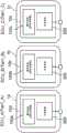
图1A是示意性示出了集成之前的ECU的配置的图。FIG. 1A is a diagram schematically showing the configuration of an ECU before integration.
图1B是示意性示出了比较例的集成ECU的配置的图。FIG. 1B is a diagram schematically showing the configuration of the integrated ECU of the comparative example.
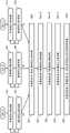
图2A是说明了由Tier1来验证图1B的集成ECU的框图。FIG. 2A is a block diagram illustrating verification of the integrated ECU of FIG. 1B by Tier1.
图2B是说明了由OEM和Tier1来验证图1B的集成ECU的框图。FIG. 2B is a block diagram illustrating validation of the integrated ECU of FIG. 1B by an OEM and Tier1.
图3是说明了图1B的集成ECU的验证的流程图。FIG. 3 is a flowchart illustrating verification of the integrated ECU of FIG. 1B .
图4是示意性示出了根据实施例的集成ECU的配置的图。FIG. 4 is a diagram schematically showing the configuration of the integrated ECU according to the embodiment.
图5是示出了单位时间内的可使用时段和使用禁止时段的图。FIG. 5 is a diagram showing a usable period and a use prohibition period in a unit time.
图6是示意性地示出了示例的集成ECU的配置的图。FIG. 6 is a diagram schematically showing the configuration of an example integrated ECU.
图7是示出了图6的控制电路的配置的框图。FIG. 7 is a block diagram showing the configuration of the control circuit of FIG. 6 .
图8是说明了图6的控制电路的操作的图。FIG. 8 is a diagram illustrating the operation of the control circuit of FIG. 6 .
图9是说明了图6的控制电路在多个单位时间内的操作的图。FIG. 9 is a diagram illustrating the operation of the control circuit of FIG. 6 for a plurality of unit times.
图10是说明了图6的集成ECU的制造方法的流程图。FIG. 10 is a flowchart illustrating a method of manufacturing the integrated ECU of FIG. 6 .
图11是示意性地示出了修改的集成ECU的配置的图。FIG. 11 is a diagram schematically showing the configuration of the modified integrated ECU.
具体实施方式Detailed ways
参考附图,下文对实施例、示例和修改进行描述。然而,在以下描述中,相同部件由相同的附图标记表示,并且可以省略其重复描述。Embodiments, examples, and modifications are described below with reference to the drawings. However, in the following description, the same components are denoted by the same reference numerals, and repeated descriptions thereof may be omitted.
首先,参考图1A和图1B对ECU的功能集成进行描述。图1A是示意性示出了集成前的ECU的配置的图,并且图1B是示意性示出了比较例的集成ECU的配置的图。First, the functional integration of the ECU will be described with reference to FIGS. 1A and 1B . FIG. 1A is a diagram schematically showing a configuration of an ECU before integration, and FIG. 1B is a diagram schematically showing a configuration of an integrated ECU of a comparative example.
如图1A所示,集成前的ECU_A1a、ECU_B1b和ECU_C1c分别主要由半导体器件10a、10b和10c组成。半导体器件10a、10b和10c中的每个半导体器件包括诸如中央处理单元(CPU)和存储器的操作资源100a、100b和100c、以及外围资源200。ECU_A1a、ECU_B1b和ECU_C1c分别由不同公司(Tier1_A、Tier1_B和Tier1_C)开发和验证。此后,由OEM组装。此时,执行与ECU_A1a、ECU_B1b和ECU_C1c的相应连接有关的部分的验证,并且完成整体功能的验证。这是因为ECU_A1a、ECU_B1b和ECU_C1c的独立性是不言而喻的。当Tier1_A、Tier1_B和Tier1_C被表示时,它们被称为Tier1。As shown in FIG. 1A, ECU_A1a, ECU_B1b and ECU_C1c before integration are mainly composed of
如图1B所示,比较例的集成ECU 1R主要由半导体器件10R构成。半导体器件10R包括用于执行ECU_A1a、ECU_B1b和ECU_C1c的功能的操作资源100以及外围资源200。例如,操作资源100以时分方式分配一个CPU和一个存储器用于ECU_A1a、ECU_B1b和ECU_C1c的功能的性能处理,并且共享外围资源200。集成ECU 1R由OEM或Tier1_A、Tier1_B和Tier1_C中的任何Tier1或另一Tier1开发和验证。然而,在Tier1_A、Tier1_B和Tier1_C的每个中开发和验证用于实现ECU_A1a、ECU_B1b和ECU_C1c的功能的软件。As shown in FIG. 1B , the integrated
参考图2A、图2B和图3,对比较例的集成ECU 1R中出现的问题进行描述。图2A是说明了由Tier1验证图1B的集成ECU的框图,并且图2B是说明了由OEM和Tier1验证图1B的集成ECU的框图。图3是说明了图1B的集成ECU的验证的流程图。Referring to FIGS. 2A , 2B and 3 , the problems occurring in the integrated
通常,每个单个ECU功能的验证通常由负责开发每个单个ECU功能的Tier1执行,并且集成状态下的验证由于其性质而由OEM执行。OEM很难执行Tier1所执行的校验。因此,在以下阶段执行对集成ECU功能的验证:(1)每个Tier1对单个ECU的功能和定时进行验证;以及(2)OEM在多个ECU被集成的状态下进行验证。In general, the verification of each individual ECU function is usually performed by Tier1 responsible for developing each individual ECU function, and the verification in the integrated state is performed by the OEM by its nature. It is difficult for the OEM to perform the verification performed by Tier1. Therefore, verification of the functions of the integrated ECUs is performed in the following stages: (1) verification of the function and timing of a single ECU per
如图2A和图3所示,在上述(1)的验证中,Tier1_A、Tier1_B和Tier1_C通过使用集成ECU 1R的硬件仅执行各自负责的软件的开发和检查。也就是说,如图3所示,Tier1_A开发用于ECU_A的功能的软件(步骤SA1),并且验证用于ECU_A的功能的软件(步骤SA2)。同样,Tier1_B开发用于ECU_B功能的软件(步骤SB1),并且验证用于ECU_B的功能的软件(步骤SB2),Tier1_C开发用于ECU_C的功能的软件(步骤SC1),并且验证用于ECU_C的功能的软件(步骤SC2)。As shown in FIGS. 2A and 3 , in the verification of the above (1), Tier1_A, Tier1_B, and Tier1_C perform only the development and inspection of the software in their respective responsibilities by using the hardware of the integrated
如图2B和图3所示,在上述(2)的验证中,OEM将由Tier1_A、Tier1_B和Tier1_C开发的软件一起安装在集成ECU 1R中,并且将其提供给每个Tier1(步骤SO1)。As shown in FIGS. 2B and 3 , in the verification of (2) above, the OEM installs the software developed by Tier1_A, Tier1_B, and Tier1_C together in the integrated
接下来,在并行操作用于ECU_A的功能的软件、用于ECU_B的功能的软件以及用于ECU_C的功能的软件的同时,Tier1_A检查(验证)用于ECU_A的功能的软件的操作(步骤SA3)。同样,Tier1_B检查(验证)用于ECU_B的功能的软件的操作(步骤SB3),并且Tier1_C检查(验证)用于ECU_C的功能的软件的操作(步骤SC3)。最后,OEM检查其中ECU_A、ECU_B和ECU_C协作的操作(步骤SO2)。Next, while operating the software for the function of ECU_A, the software for the function of ECU_B, and the software for the function of ECU_C in parallel, Tier1_A checks (verifies) the operation of the software for the function of ECU_A (step SA3 ) . Likewise, Tier1_B checks (verifies) the operation of the software for the function of ECU_B (step SB3 ), and Tier1_C checks (verifies) the operation of the software for the function of ECU_C (step SC3 ). Finally, the OEM checks the operation in which ECU_A, ECU_B and ECU_C cooperate (step SO2).
步骤SA1、SA2、SB1、SB2、SC1和SC2与Tier1对未集成的ECU所执行的设计和验证相同。步骤SO1和SO2与OEM对未集成的ECU所执行的验证相同。步骤SA3、SB3和SC3是通过集成而被增加的、Tier1所执行的校验。这是由于以下原因。Steps SA1, SA2, SB1, SB2, SC1 and SC2 are the same as the design and verification performed by Tier1 for the unintegrated ECU. Steps SO1 and SO2 are the same as the verification performed by the OEM for a non-integrated ECU. Steps SA3, SB3, and SC3 are verifications performed by Tier1, which are added by integration. This is due to the following reasons.
尽管在单个ECU功能评估的情况下可以占用外围资源200,但是当执行ECU集成时,外围资源200由每个单个ECU功能共享。因此,尽管执行了单个ECU的功能和定时的验证,但是发生了外围资源200的冲突,因此,即使在功能被集成的环境中,也需要确认执行与单个ECU验证时的操作相同的操作。换句话说,在单独执行验证之后,必须重新验证功能被集成的状态。Although
为了实现其中集成多个ECU功能的集成ECU,必须的是当在上述(2)中通过集成多个ECU功能来执行验证时,可以使用在上述(1)中执行的验证的结果(上述(1)中的验证不是必需的)。换句话说,需要执行上述(1)的验证,使得在验证上述(2)时可以利用上述(1)的验证结果。In order to realize an integrated ECU in which a plurality of ECU functions are integrated, it is necessary that when verification is performed by integrating a plurality of ECU functions in the above (2), the result of the verification performed in the above (1) can be used (the above (1) ) is not required). In other words, the verification of the above (1) needs to be performed so that the verification result of the above (1) can be used when verifying the above (2).
因此,在集成ECU中,当Tier1验证单个ECU功能时,需要能够在共享外围资源的条件下执行验证。Therefore, in an integrated ECU, when Tier1 verifies a single ECU function, it needs to be able to perform the verification under the condition of sharing peripheral resources.
实施例Example
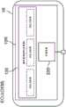
参照图4,对根据实施例的集成ECU进行描述,该集成ECU中,集成了图1A的单个ECU_A1a、单个ECU_B1b和单个ECU_C1c。图4是示意性示出了根据实施例的集成ECU的配置的图。Referring to FIG. 4 , an integrated ECU in which a single ECU_A1 a , a single ECU_B1 b , and a single ECU_C1 c of FIG. 1A are integrated according to an embodiment will be described. FIG. 4 is a diagram schematically showing the configuration of the integrated ECU according to the embodiment.
根据实施例的集成ECU 1主要由半导体器件10构成。半导体器件10包括:操作资源100,用于执行ECU_A1a、ECU_B1b和ECU_C1c的功能;外围资源200;以及控制机构300,用于控制外围资源200。例如,操作资源100以时分方式分配一个CPU和一个存储器用于操作资源100a、100b和100c的处理,并且外围资源200由操作资源100a、100b和100c共享。应当指出,操作资源100可以由多个CPU配置。The
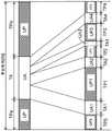
接下来,参照图5,对图4的控制机构的功能进行描述。图5是示出了单位时间内的可使用时段和使用禁止时段的图。Next, with reference to FIG. 5 , the function of the control mechanism of FIG. 4 will be described. FIG. 5 is a diagram showing a usable period and a use prohibition period in a unit time.
控制机构300通过在上述(1)的单个ECU功能验证时共享外围资源200来创建争用状态。The
例如,控制机构300创建与提前分配给共享的外围资源200的预算值(BDG)相对应的使用禁止状态,从而在集成时实现的使用频率内实现单个ECU的验证。根据每个单个ECU的限制要求(每个单个ECU的性能分配)确定BDG的设置。外围资源200处于使用禁止状态的时段被称为使用禁止时段UP,并且外围资源200处于可用状态的时段被称为可用时段UA。假设单位时间(UNIT TIME)的时间为TU,使用禁止时段UP的时间为TP,使用禁止时段UP的第一时间为TPa,使用禁止时段UP的第二时间为TPb,以及可用时段UA的时间为TA,For example, the
TU=TA+TPa+TPb=TA+TP,以及TU=TA+TPa+TPb=TA+TP, and
BDG=TA/(TPa+TPb)=TA/TP。BDG=TA/(TPa+TPb)=TA/TP.
本文中,当TP=TPa+TPb时,TP=TU/(1+BDG)。Here, when TP=TPa+TPb, TP=TU/(1+BDG).
基于单位时间(TU)和预算值(BDG)来确定使用禁止时段UP的时间(TP)和可用时段UA的时间(TA)。结果,控制机构300在单个ECU功能评估时使得外围资源200仅能够在限定频带中可用。The time (TP) of the use prohibition period UP and the time (TA) of the available period UA are determined based on the unit time (TU) and the budget value (BDG). As a result, the
由于外围资源200可以在预算值内离散使用,所以它与仅提供一个可用时段不一致。因此,例如,控制机构300可以进行以下操作:将可用时段UA划分为第一可用时段UA1、第二可用时段UA2、第三可用时段UA3和第四可用时段UA4;将使用禁止时段UP划分为第一使用禁止时段UP1、第二使用禁止时段UP2、第三使用禁止时段UP3、第四使用禁止时段UP4和第五使用禁止时段UP5;并且使得可用时段UA得以分散。本文中,当第一可用时段UA1的时间为TA1时,第二可用时段UA2的时间为TA2,第三可用时段UA3的时间为TA3,第四可用时段UA4的时间为TA4,第一使用禁止时段UP1的时间是TP1,第二使用禁止时段UP2的时间是TP2,第三使用禁止时段UP3的时间是TP3,第四使用禁止时段UP4的时间是TP4,并且第五使用禁止时段UP5的时间是TP5,Since the
TA=TA1+TA2+TA3+TA4,以及TA=TA1+TA2+TA3+TA4, and
TP=TPa+TPb=TP5+TP1+TP2+TP3+TP4。TP=TPa+TPb=TP5+TP1+TP2+TP3+TP4.
例如,确定使用禁止时段如下:For example, determine the usage prohibition period as follows:
(a)基于外围资源200的使用时间来动态插入外围资源200的使用禁止时段。使用禁止时段的时间基于预算值来计算。当执行单个ECU功能评估时,这使得可以提供与集成ECU中的外围资源的使用率相同的外围资源的使用率。(a) Dynamic insertion of the usage prohibition period of the
(b)在使用外围资源200之后,使用禁止时段基于使用时间而被设置,并且被插入。优选地,使用禁止时段(例如,时间(TP1)的第一使用禁止时段UP1)基于紧接地在前的使用时间(例如,第一可用时段UA1的时间(TA1))而被设置,并且被插入。结果,可以为经过验证的单个ECU功能提供离散使用外围资源的机会。(b) After the
此外,由于其自身的处理内容的约束,单个ECU功能可能无法连续访问外围资源200。没有执行该访问的状态被称为不可访问状态,并且该时段被称为不可访问时段。如果除了使用禁止时段期间之外存在没有使用外围资源200,则可以从“使用禁止时段”中减去未进行这种使用的时段,并且经过验证的单个ECU功能可能拥有的不可访问时段不会被记录为使用禁止时段。由于经过验证的单个ECU功能可能拥有的不可访问时段没有被包括在可用时段中,因此经过验证的单个ECU功能可能拥有的不可访问时段被记录为使用禁止时段,因此,未设置过多的使用禁止时段。Furthermore, a single ECU function may not be able to continuously access
控制机构300可以由硬件或软件配置。外围资源是诸如输入/输出(I/O)的用于实现半导体器件的输入或输出接口功能的电路,外围设备(诸如用于与另一ECU等进行通信的通信控制器、传感器、开关、致动器等)被连接到该电路;并且外围资源是可以由多个ECU功能共享的电路。在以下示例中,将描述根据实施例的控制机构300由硬件配置的情况以及外围资源是通信控制器的情况。The
示例Example
图6是示意性示出了示例的集成ECU的配置的图。如图6所示,集成ECU 1A被连接到作为车载网络的控制器局域网(CAN)总线2a,并且可以与另一ECU等进行通信。集成ECU1A可以经由调试器接口(I/F)4连接到调试器3。FIG. 6 is a diagram schematically showing the configuration of an example integrated ECU. As shown in FIG. 6, the integrated ECU 1A is connected to a controller area network (CAN) bus 2a as an in-vehicle network, and can communicate with another ECU or the like. The integrated ECU 1A can be connected to the debugger 3 via a debugger interface (I/F) 4 .
ECU 1A主要由诸如微控制器或片上系统(SOC)的半导体器件10A、以及收发器集成电路(IC)20a组成。半导体器件10A包括:CPU 101;存储单元102,用于存储用于实现单个ECU功能中的每个ECU功能的软件程序102a、102b和102c;用于CAN通信的通信控制器(通信外围电路)200a;控制电路300a;控制电路500;以及定时器600。操作资源100由CPU 101和存储单元102组成,并且CPU 101以时分方式执行存储在存储单元102中的软件程序102a、102b和102c,从而配置ECU_A1a、ECU_B1b和ECU_C1c的功能。与实施例的外围资源200类似地共享通信外围电路200a。操作资源100可以由多个CPU组成。存储单元102包括例如非易失性存储器(诸如闪存)和易失性存储器(诸如静态随机存取存储器(SRAM))。The ECU 1A is mainly composed of a
单个ECU功能由操作资源100执行,并且根据需要通过通信外围电路200a与集成ECU 1A的外部通信。A single ECU function is performed by the
通信外围电路200a根据CAN的通信协议将传输缓冲器(未示出)的帧转换为串行传输信号,并且将该串行传输信号输出到收发器IC 20a。收发器IC 20a将从通信外围电路200a获得的逻辑电平的传输信号转换为对应差分电压,并且将该差分电压传输到CAN总线2a。The communication
在数据接收时,收发器IC 20a读取CAN总线2a的差分电压,并且将接收信号输出到通信外围电路200a,该接收信号被成形为被包括在预定电压范围内。通信外围电路200a的接收端子包括例如比较器,将预定的阈值电压与来自收发器IC 20a的接收信号进行比较以生成数字数据“1”和“0”,并且将该数字数据存储在接收缓冲器(未示出)中。At the time of data reception, the
控制电路300a设置用于通信外围电路200a的使用禁止时段,并且由于通信外围电路200a中的共享而形成争用状态。在满足以下条件的状态下,设置使用禁止时段。The
(I)考虑到在使用后立即按优先级排列对其他进程的分配(I) Take into account the allocation to other processes by priority immediately after use
(II)考虑单个ECU本身的不可访问状态(II) Consider the inaccessible state of a single ECU itself
具体地,控制电路300a:Specifically, the
(A)将使用禁止状态/可用状态通知给通信外围电路200a,并且将通信外围电路200a设置为使用禁止状态;(A) Notifying the communication
(B)通过预定的约束(预算值)计算通信外围电路200a的使用禁止状态;(B) calculating the use prohibition state of the communication
(C)通过预定的约束(预算值)和过去操作的通信外围电路200a的使用时间来设置下一使用禁止状态的时段(使用禁止时段);以及(C) setting the period of the next use prohibition state (use prohibition period) by a predetermined constraint (budget value) and the use time of the communication
(D)从使用禁止时段中去除通信外围电路200a的不可访问时间。(D) The inaccessible time of the communication
通信外围电路200a被配置为:例如,当从控制电路300a通知了使用禁止时,响应于来自CPU 101的访问请求信号,而不会输出确认信号,并且通信外围电路200a被配置为:当通知了可用状态时,输出确认信号。The communication
接下来,参照图7,对控制电路300a的配置进行描述。图7是示出了图6的控制电路300a的配置的框图。Next, with reference to FIG. 7, the configuration of the
控制电路300a包括:计数器301,用于测量通信外围电路200a的操作时间;以及主计数器302,用于确定通信外围电路200a是否可用。控制电路300a:The
(i)在不使用通信外围电路200a的时段期间对主计数器302进行向下计数;(i) count down the
(ii)当主计数器302的计数值为负时,使通信外围电路200a可用,并且当计数值为正时,禁用通信外围电路200a;(ii) enabling the communication
(iii)在使用通信外围电路200a的同时,停止主计数器302;以及(iii) while using the communication
(iv)在使用通信外围电路200a之后,根据使用率将主计数器302的计数值相加。(iv) After the communication
计数器301包括计数器寄存器(CNTR)301a、增量器(INC)301b、以及选择器301c。通过断言来自通信外围电路200a的传送结束信号(SC1)或来自定时器600的复位信号(SC2)来初始化计数器301。这通过以下方式来执行:选择器301c通过传送结束信号(SC1)或复位信号(SC2)选择“0”并且将所选择的“0”输入到计数器寄存器(CNTR)301a。在通信外围电路200a正在操作的同时,计数器301继续向上计数。这通过以下方式来执行:选择器301c响应于指示通信外围电路200a处于操作中的操作中信号(SC3)来选择增量器301b的输出,并且将所选择的、增量器301b的输出输入到计数器寄存器(CNTR)301a。结果,当生成传送结束信号(SC1)时,计数器301指示使用通信外围电路200a的占用时间。The
主计数器302包括主计数器寄存器(MCNTR)302a、减量器(DEC)302b、选择器302c、乘法器302d、寄存器302e、加法器302f、以及负确定器302g。通过周期性复位信号(SC2)对主计数器302进行初始化。这通过以下方式来执行:选择器302c通过复位信号(SC2)选择“0”并且将所选择的“0”输入到主计数器寄存器(MCNTR)302a。假定复位信号(SC2)的周期是单位时间(UNIT TIME),当通信外围电路200a被控制时,所分配的频带要针对该单位时间而被保证。The
当通信外围电路200a不操作时,主计数器302用作减法计数器。这通过以下方式来执行:选择器302c响应于指示通信外围电路200a处于操作中的操作中信号(SC3)来选择减量器302b的输出,并且将减量器302b的所选择的输出输入到主计数器寄存器(MCNTR)302a。When the communication
当生成传送结束信号(SC1)时,主计数器302使用乘法器302d将计数器寄存器(CNTR)301a的值乘以预算值(SC4),并且使用加法器302f将运算结果与主计数器寄存器(MCNTR)302a的值相加,该预算值(SC4)是由控制电路500提前在寄存器302e中设置的系数(因子)。这通过以下方式执行:选择器302c响应于传送结束信号(SC1)来选择加法器302f的输出,并且将所选择的、加法器302f的输出输入到主计数器寄存器(MCNTR)302a。When the transfer end signal (SC1) is generated, the
负确定器(<0)302g确定主计数器寄存器(MCNTR)302a的值是否为负,并且向通信外围电路200a输出可用信号(SC5)。如果负确定器302g确定主计数器寄存器(MCNTR)302a的值为负,则断言可用信号(SC5),并且通信外围电路200a可用。如果负确定器302g确定主计数器寄存器(MCNTR)302a的值为正(不为负),则可用信号(SC5)被否定并且通信外围电路200a不可用。负确定器302g例如依据主计数器寄存器(MCNTR)302a的最高有效位是否为“1”来确定主计数器寄存器(MCNTR)302a的值是否为负。Negative determiner (<0) 302g determines whether or not the value of main counter register (MCNTR) 302a is negative, and outputs an available signal to communication
如图6所示,经由调试器I/F 4,从调试器3向控制电路300a设置预算值和单位时间(周期)。该设置由OEM通过静态值指示给相应Tier1。控制电路500在控制电路300a的寄存器302e中设置由调试器3设置的预算值(SC4)。控制电路500向定时器600设置由调试器3设置的单位时间。定时器600每个单位时间生成复位信号(SC1)。As shown in FIG. 6 , a budget value and a unit time (cycle) are set from the debugger 3 to the
注意,控制电路300a、控制电路500、定时器600和调试器3仅在Tier1的单元ECU功能评估时被使用,并且不会在OEM的评估时或批量生产和运输之后被使用。Note that the
接下来,参照图8和图9,对控制电路300a的操作进行详细描述。图8是用于说明图6的控制电路300a的操作的图。图9是用于说明图6的控制电路300a在多个单位时间内的操作的图。图8示出了其中在单位时间(UNIT TIME)内发生通信外围电路200a的使用(访问请求)α、β和γ的示例。Next, with reference to FIGS. 8 and 9, the operation of the
尽管在单位时间的开始设置了可用时段UA,但是CPU 101对于通信外围电路200a不可用,并且在变得可用之后,生成初始访问请求α。假定针对访问请求α使用通信外围电路200a所花费的时间是Tα。Although the availability period UA is set at the beginning of the unit time, the
通过来自通信外围电路200a的传送结束事件信号(SC1)来设置用于通信外围电路200a的使用禁止时段PB,并且主计数器302开始减法。The use prohibition period PB for the communication
虽然主计数器寄存器(MCNTR)302a的值取正值,但是通信外围电路200a被禁用,并且等待直到主计数器寄存器(MCNTR)302a的值呈现负数所生成的访问请求β的通信外围电路200a的使用,直到主计数器寄存器(MCNTR)302a的值变为负为止。Although the value of the main counter register (MCNTR) 302a takes a positive value, the communication
从通信外围电路200a的紧接在前使用时的处理所花费的时间(Tα)导出通信外围电路200a的使用禁止时段PB的时间(TB)。如果通信外围电路200a对要作为目标的单个ECU功能的使用分配(系数(因子))是K%,则从将Tα乘以(100-K)/K获得的时间导出TB的值。例如,当K=25时,TB=3×Tα。The time (TB) of the use prohibition period PB of the communication
当主计数器寄存器(MCNTR)302a的值变为负值时,通信外围电路200a变为可用,并且开始针对访问请求β的通信外围电路200a的使用。When the value of the main counter register (MCNTR) 302a becomes a negative value, the communication
通信外围电路200a针对访问请求β的使用所需的时间由计数器301进行计数。在该时间期间,主计数器302不会递减,并且主计数器寄存器(MCNTR)302a的值保持不变。The time required for the use of the access request β by the communication
从使用通信外围电路200a针对访问请求β的使用所花费的时间(Tβ),再次计算通信外围电路200a的使用禁止时段PC的时间(TC),并且将该时间(TC)添加到主计数器寄存器(MCNTR)302a。主计数器302开始,并且继续减法计数过程。From the time (Tβ) it takes for the use of the access request β by the use of the communication
尽管在使用禁止时段PC的时间(TC)过去之后设置了可用时段UA,但是主计数器302继续递减,因为没有对通信外围电路200a的后续访问请求。Although the available period UA is set after the time (TC) of the use prohibition period PC elapses, the
如果从先前访问请求β经过了TD时间(比TC时间长)之后出现访问请求γ,则访问请求γ可以立即开始使用通信外围电路200a。这是因为主计数器寄存器(MCNTR)302a的值指示负数。If the access request γ occurs after the TD time (longer than the TC time) has elapsed from the previous access request β, the access request γ can immediately start using the communication
在完成通信外围电路200a针对访问请求γ的使用之后,从通信外围电路200a针对访问请求γ的使用中所重新计算的使用禁止时段PE的时间(TE)被计算,并且被添加到主计数器寄存器(MCNTR)302a。由于从通信外围电路200a针对访问请求γ的使用所花费的时间(Tγ)中计算出的使用禁止时段PE的时间(TE)被添加到作为负数的主计数器寄存器(MCNTR)302a,所以从主计数器寄存器(MCNTR)302a确定的通信外围电路200a的使用禁止时段PE是通过减去过去时间(TD)与时间(TC)之间的差而获得的时间(TE)。可以在执行上述校正的使用禁止时段PE已过去之后发出对通信外围电路200a的后续访问请求。After the use of the communication
如图9所示,在经过了要确立通信外围电路200a的频带保证的最小单位时间(UNITTIME)之后,不管主计数器302的状态如何,都由复位信号(SC2)来初始化主计数器302。在图9的第一单位时间内,设置了不可访问时段UN、使用时段A、使用禁止时段P……以及不可访问时段UN,并且尽管主计数器寄存器(MCNTR)302a取负数,经过单位时间之后的复位信号在不可访问时段UN期间被输入。本文中,可用时段UA包括使用时段A和不可访问时段UN。在第二单位时间开始时,第一单位时间的不可访问时段UN继续。经过第二单位时间之后的复位信号也在不可访问时段UN期间被输入。然而,在第三单位时间开始时,设置使用时段A。控制电路300a每经过单位时间就对主计数器302进行初始化,并且抑制在单位时间内发生超出预算分配的访问。As shown in FIG. 9, after the minimum unit time (UNITTIME) for establishing the bandwidth guarantee of the communication
图10是说明了图6的集成ECU 1A的制造方法的流程图。OEM开发和制造集成ECU 1A的硬件。集成ECU 1A中的半导体器件10A例如由半导体制造商等制造。使用从OEM租用的集成ECU 1A的硬件,Tier1_A、Tier1_B和Tier1_C仅对各自负责的软件执行开发和操作检查。也就是说,如图10所示,Tier1_A开发用于ECU_A的功能的软件(步骤SA11),验证用于ECU_A的功能的软件(步骤SA12),并且将该软件交付给OEM。同样,Tier1_B开发用于ECU_B的功能的软件(步骤SB11),验证用于ECU_B的功能的软件(步骤SB12),并且将该软件交付给OEM。Tier1_C开发用于ECU_C的功能的软件(步骤SC11),验证用于ECU_C的功能的软件(步骤SC12),并且将该软件交付给OEM。相应Tier1可以在集成状态下验证单个ECU的功能。FIG. 10 is a flowchart illustrating a method of manufacturing the integrated ECU 1A of FIG. 6 . OEM develops and manufactures hardware integrating ECU 1A. The
如图10所示,OEM将由Tier1_A、Tier1_B和Tier1_C开发和验证的软件安装在集成ECU1中(步骤SO11)。OEM在并行操作ECU_A、ECU_B和ECU_C功能的同时,与ECU_A/ECU_B/ECU_C协作检查ECU_A/ECU_B/ECU_C的操作(步骤SO12)。注意,步骤SO11和步骤SO12之间无需通过Tier1进行图3的步骤SA3、SB3、SC3。As shown in FIG. 10, the OEM installs the software developed and verified by Tier1_A, Tier1_B, and Tier1_C in the integrated ECU1 (step SO11). The OEM checks the operation of ECU_A/ECU_B/ECU_C in cooperation with ECU_A/ECU_B/ECU_C while operating the functions of ECU_A, ECU_B, and ECU_C in parallel (step SO12). Note that steps SA3, SB3, and SC3 of FIG. 3 need not be performed through Tier1 between steps SO11 and SO12.
在该示例中,在向集成ECU提供的半导体中,安装了用于向通信外围电路提供一定的“使用禁止时段”的“控制机构”。In this example, in the semiconductor provided to the integrated ECU, a "control mechanism" for providing a certain "use prohibition period" to the communication peripheral circuit is installed.
进一步地,根据作为目标的通信外围电路的过去占用时间和在单个ECU功能评估之前确定的“频带分配”来确定“使用禁止时段”。该功能确保即使在集成ECU中,还完成了集成ECU时预期的“频带”内的处理。Further, the "use prohibition period" is determined based on the past occupancy time of the target communication peripheral circuit and the "band allocation" determined before the individual ECU function evaluation. This function ensures that even in the integrated ECU, the processing within the "band" expected when the ECU is integrated is done.
进一步地,由于与通信外围电路的紧接在前的使用时间协作设置了使用禁止时段,所以在离散定时处执行使用禁止时段的插入。在避免了长时间时段内的通信外围电路的使用禁止状态的同时,可以实现单个ECU评估。Further, since the use prohibition period is set in cooperation with the immediately preceding use time of the communication peripheral circuit, the insertion of the use prohibition period is performed at discrete timings. A single ECU evaluation can be achieved while avoiding the use-prohibited state of the communication peripheral circuit for a long period of time.
通过从控制电路所设置的“使用禁止时段”中减去单个ECU功能的可能的不可访问时段,避免过度设置使用禁止时段。这是因为当作为集成ECU操作时,即使在单个ECU功能的“使用禁止时段”期间,也可以执行来自其他单个ECU功能的访问。Excessive setting of the use prohibition period is avoided by subtracting the possible inaccessibility period of a single ECU function from the "use prohibition period" set by the control circuit. This is because when operating as an integrated ECU, access from other single ECU functions can be performed even during the "use prohibition period" of a single ECU function.
修改Revise
下文对几个示例性修改进行说明。在以下修改说明中,与上文所提及的示例相同的附图标记可以用于具有与上文所提及的示例中所描述的结构和功能相同的结构和功能的部件。在对这些部分的描述中,上文所提及的示例中的描述可以适当地并入与技术方面不矛盾的范围内。另外,上文所提及的示例的一部分和多个修改的全部或一部分可以在与技术方面不矛盾的范围内适当地组合应用。Several exemplary modifications are described below. In the following modification descriptions, the same reference numerals as in the above-mentioned examples may be used for components having the same structures and functions as those described in the above-mentioned examples. In the description of these parts, the descriptions in the above-mentioned examples may be appropriately incorporated within the scope not inconsistent with the technical aspects. In addition, a part of the above-mentioned examples and all or part of a plurality of modifications can be applied in combination as appropriate within a range that does not contradict the technical aspects.
在该示例中,用于CAN通信的通信控制器(通信外围电路)作为外围资源的示例,但是通信外围电路可以是用于FlexRay通信、本地互连网络(LIN)通信、以太网通信等的电路。外围资源的数目不限于一个,并且可以使用多个外围资源。在下文中,参照图11,对包括用于CAN通信的通信控制器和用于以太网通信的通信控制器的两个通信外围电路的情况(修改)进行描述。In this example, a communication controller (communication peripheral circuit) for CAN communication is used as an example of a peripheral resource, but the communication peripheral circuit may be a circuit for FlexRay communication, Local Interconnect Network (LIN) communication, Ethernet communication, or the like . The number of peripheral resources is not limited to one, and a plurality of peripheral resources may be used. Hereinafter, referring to FIG. 11 , a case (modification) of two communication peripheral circuits including a communication controller for CAN communication and a communication controller for Ethernet communication will be described.
图11是示意性地示出了修改的集成ECU的配置的图。FIG. 11 is a diagram schematically showing the configuration of the modified integrated ECU.
如图11所示,集成ECU 1B被连接到作为车载网络的两条车载网络线路,即,CAN总线2a和以太网总线2b,并且可以与另一ECU等通信。集成ECU 1B主要由诸如微控制器或SOC的半导体器件10B、以及收发器IC 20a和20b组成。在一个半导体芯片中,半导体器件10B包括:CPU 101;存储单元102,存储用于实现每个单个ECU功能的软件程序102a、102b和102c;用于CAN通信的通信控制器(通信外围电路)200a;用于以太网通信的通信控制器(通信外围电路)200b;以及控制电路300a和300b。操作资源100由CPU 101和存储单元102组成,并且CPU 101以时分方式执行存储在存储单元102中的软件程序102a、102b和102c,以配置ECU_A1a、ECU_B1和ECU_C1c的功能。与实施例的外围资源200类似地共享通信外围电路200a和200b。操作资源100可以由多个CPU组成。存储单元102包括例如非易失性存储器(诸如闪存)和易失性存储器(诸如SRAM)。As shown in FIG. 11, the integrated
单个ECU功能由操作资源100执行,并且根据需要通过通信外围电路200a和200b与集成ECU 1B的外部通信。A single ECU function is performed by the
尽管已经基于实施例、示例和修改对由本发明人做出的发明进行了具体描述,但是不言而喻的是,本发明不限于上述实施例、示例和修改,并且可以以各种形式进行修改。Although the invention made by the present inventors has been specifically described based on the embodiments, examples, and modifications, it goes without saying that the present invention is not limited to the above-described embodiments, examples, and modifications, and can be modified in various forms .
例如,在实施例、示例和修改中,已经描述了集成三个单个ECU功能的情况,但是本发明不限于此,并且可以应用于其中集成两个或更多个单个ECU功能的情况。For example, in the embodiments, examples, and modifications, the case where three single ECU functions are integrated has been described, but the present invention is not limited thereto and can be applied to the case where two or more single ECU functions are integrated.
Claims (11)
Translated fromChineseApplications Claiming Priority (2)
| Application Number | Priority Date | Filing Date | Title |
|---|---|---|---|
| JP2018-236819 | 2018-12-18 | ||
| JP2018236819AJP7141942B2 (en) | 2018-12-18 | 2018-12-18 | Semiconductor equipment and electronic control equipment |
Publications (2)
| Publication Number | Publication Date |
|---|---|
| CN111338314Atrue CN111338314A (en) | 2020-06-26 |
| CN111338314B CN111338314B (en) | 2024-07-16 |
Family
ID=68655292
Family Applications (1)
| Application Number | Title | Priority Date | Filing Date |
|---|---|---|---|
| CN201911135160.6AActiveCN111338314B (en) | 2018-12-18 | 2019-11-19 | Semiconductor device, electronic control unit, verification method of electronic control unit, and manufacturing method of electronic control unit |
Country Status (4)
| Country | Link |
|---|---|
| US (2) | US11358546B2 (en) |
| EP (1) | EP3671446B1 (en) |
| JP (1) | JP7141942B2 (en) |
| CN (1) | CN111338314B (en) |
Families Citing this family (1)
| Publication number | Priority date | Publication date | Assignee | Title |
|---|---|---|---|---|
| CN111766848B (en)* | 2020-06-29 | 2021-09-10 | 北京广利核系统工程有限公司 | Method and device for verifying failure rate of subsystem in instrument control system |
Citations (8)
| Publication number | Priority date | Publication date | Assignee | Title |
|---|---|---|---|---|
| CN1529854A (en)* | 2001-11-30 | 2004-09-15 | ��ʿͨ��ʽ���� | Microcomputer logic development device |
| US20090037046A1 (en)* | 2007-08-03 | 2009-02-05 | Denso Corporation | Electronic control unit |
| US20090217280A1 (en)* | 2008-02-21 | 2009-08-27 | Honeywell International Inc. | Shared-Resource Time Partitioning in a Multi-Core System |
| CN101996146A (en)* | 2009-08-26 | 2011-03-30 | 戴尔产品有限公司 | Multi-mode processing module and using method thereof |
| US20160323283A1 (en)* | 2015-04-30 | 2016-11-03 | Samsung Electronics Co., Ltd. | Semiconductor device for controlling access right to resource based on pairing technique and method thereof |
| KR20160129663A (en)* | 2015-04-30 | 2016-11-09 | 삼성전자주식회사 | Semiconductor device of controlling access right for resource based on pairing technigue and method thereof |
| JP2017177410A (en)* | 2016-03-29 | 2017-10-05 | 富士ゼロックス株式会社 | Control device and printer |
| CN108363347A (en)* | 2017-01-27 | 2018-08-03 | 李尔公司 | Hardware security for electronic control unit |
Family Cites Families (19)
| Publication number | Priority date | Publication date | Assignee | Title |
|---|---|---|---|---|
| JP2001282710A (en)* | 2000-03-31 | 2001-10-12 | Brother Ind Ltd | Circuit and method for arbitrating bus use |
| US7353217B2 (en)* | 2001-06-01 | 2008-04-01 | Texas Instruments Incorporated | Intelligent realtime management of processing resources |
| JP4282472B2 (en)* | 2003-12-26 | 2009-06-24 | 株式会社東芝 | Microprocessor |
| JP4624448B2 (en)* | 2008-07-30 | 2011-02-02 | 株式会社オートネットワーク技術研究所 | Control device, control system, and computer program |
| JP2011028559A (en)* | 2009-07-27 | 2011-02-10 | Denso Corp | Relay program and electronic control device |
| JP2011216004A (en)* | 2010-04-01 | 2011-10-27 | Toyota Motor Corp | Microprocessor, electronic control unit, execution ratio switching method |
| JP2012114724A (en) | 2010-11-25 | 2012-06-14 | Toyota Motor Corp | Electronic control device |
| JP5850774B2 (en)* | 2012-03-22 | 2016-02-03 | ルネサスエレクトロニクス株式会社 | Semiconductor integrated circuit device and system using the same |
| US10643403B2 (en)* | 2012-08-20 | 2020-05-05 | Innova Electronics Corporation | Predictive diagnostic method and system |
| JP5870968B2 (en)* | 2013-06-03 | 2016-03-01 | 株式会社デンソー | Wire harness evaluation device |
| US9372725B2 (en)* | 2014-02-19 | 2016-06-21 | International Business Machines Corporation | Dynamically adjusting wait periods according to system performance |
| WO2018096755A1 (en)* | 2016-11-25 | 2018-05-31 | 株式会社デンソー | Parallel processing device and parallel processing program |
| EP3343366B1 (en)* | 2016-12-27 | 2020-12-30 | OpenSynergy GmbH | System and method for scheduling a plurality of guest systems and/or threads |
| JP7316609B2 (en)* | 2017-01-05 | 2023-07-28 | ガードノックス・サイバー・テクノロジーズ・リミテッド | Centralized service ECU based on service-oriented architecture and its usage |
| JP7006461B2 (en)* | 2018-04-02 | 2022-01-24 | 株式会社デンソー | Electronic control device and electronic control system |
| EP3572939A1 (en)* | 2018-05-25 | 2019-11-27 | TTTech Auto AG | Method, device and real-time network for highly-integrated automotive systems |
| US20210358025A1 (en)* | 2020-05-15 | 2021-11-18 | Toyota Motor Engineering & Manufacturing North America, Inc. | Vehicle sharing systems and methods for matching available vehicles to user requests |
| US11614962B2 (en)* | 2020-06-25 | 2023-03-28 | Toyota Motor Engineering & Manufacturing North America, Inc. | Scheduling vehicle task offloading and triggering a backoff period |
| US11531566B2 (en)* | 2020-07-10 | 2022-12-20 | Infineon Technologies Ag | Safe and secure communication network message processing |
- 2018
- 2018-12-18JPJP2018236819Apatent/JP7141942B2/enactiveActive
- 2019
- 2019-11-06USUS16/676,047patent/US11358546B2/enactiveActive
- 2019-11-19CNCN201911135160.6Apatent/CN111338314B/enactiveActive
- 2019-11-25EPEP19211093.0Apatent/EP3671446B1/enactiveActive
- 2022
- 2022-05-16USUS17/745,253patent/US11845387B2/enactiveActive
Patent Citations (8)
| Publication number | Priority date | Publication date | Assignee | Title |
|---|---|---|---|---|
| CN1529854A (en)* | 2001-11-30 | 2004-09-15 | ��ʿͨ��ʽ���� | Microcomputer logic development device |
| US20090037046A1 (en)* | 2007-08-03 | 2009-02-05 | Denso Corporation | Electronic control unit |
| US20090217280A1 (en)* | 2008-02-21 | 2009-08-27 | Honeywell International Inc. | Shared-Resource Time Partitioning in a Multi-Core System |
| CN101996146A (en)* | 2009-08-26 | 2011-03-30 | 戴尔产品有限公司 | Multi-mode processing module and using method thereof |
| US20160323283A1 (en)* | 2015-04-30 | 2016-11-03 | Samsung Electronics Co., Ltd. | Semiconductor device for controlling access right to resource based on pairing technique and method thereof |
| KR20160129663A (en)* | 2015-04-30 | 2016-11-09 | 삼성전자주식회사 | Semiconductor device of controlling access right for resource based on pairing technigue and method thereof |
| JP2017177410A (en)* | 2016-03-29 | 2017-10-05 | 富士ゼロックス株式会社 | Control device and printer |
| CN108363347A (en)* | 2017-01-27 | 2018-08-03 | 李尔公司 | Hardware security for electronic control unit |
Non-Patent Citations (2)
| Title |
|---|
| MATTHIAS BECKERT 等: "Exploiting sporadic servers to provide budget scheduling for ARINC653 based real-time virtualization environments", 《DESIGN, AUTOMATION AND TEST IN EUROPE (DATE)》, pages 870 - 875* |
| THOMAS NOLTE 等: "A Synchronization Protocol for Temporal Isolation of Software Components in Vehicular Systems", 《IEEE TRANSACTIONS ON INDUSTRIAL INFORMATICS》, vol. 5, no. 4, pages 375 - 387, XP011278351, DOI: 10.1109/TII.2009.2033267* |
Also Published As
| Publication number | Publication date |
|---|---|
| EP3671446B1 (en) | 2025-01-22 |
| US11358546B2 (en) | 2022-06-14 |
| EP3671446A1 (en) | 2020-06-24 |
| JP2020098507A (en) | 2020-06-25 |
| US20200189497A1 (en) | 2020-06-18 |
| JP7141942B2 (en) | 2022-09-26 |
| CN111338314B (en) | 2024-07-16 |
| US20220274546A1 (en) | 2022-09-01 |
| US11845387B2 (en) | 2023-12-19 |
Similar Documents
| Publication | Publication Date | Title |
|---|---|---|
| US11256651B2 (en) | Multiple master, multi-slave serial peripheral interface | |
| US9281718B2 (en) | On-board power supply monitor and power control system | |
| CN112099465A (en) | Vehicle diagnosis communication device and method, and system including vehicle diagnosis communication device | |
| JP5338819B2 (en) | Clock dividing circuit and clock dividing method | |
| EP3343373A1 (en) | Semiconductor device comprising watchdog timer | |
| KR20070018595A (en) | System and method for arbitrating requests for access to shared resources | |
| US11845387B2 (en) | Semiconductor device, electronic control unit, verification method of electronic control unit and manufacturing method of electronic control unit | |
| JP2002158567A (en) | Generation of pulse signal from clock signal | |
| KR101692114B1 (en) | Apparatus and method for diagnosing errors of task execution | |
| JP2023552627A (en) | Method for optimizing transfer data rate in sensor networks in partial network operation in Ethernet networks | |
| JP4425598B2 (en) | Arbitration parameter generation circuit, bus use parameter generation circuit, system on chip, arbitration parameter generation method, and bus use parameter generation method | |
| US11695590B2 (en) | Communication device, communication system and message arbitration method | |
| US11342960B2 (en) | Relay device, relay method, and computer program | |
| Mubeen et al. | Modeling of end-to-end resource reservations in component-based vehicular embedded systems | |
| EP3680782B1 (en) | Secure element with customisable functions and corresponding method | |
| EP3971721B1 (en) | Information processing device | |
| CN114126929A (en) | Control device and method for activating passenger protection means of a vehicle | |
| JP5472487B2 (en) | Semiconductor device and information processing apparatus | |
| JP7056205B2 (en) | Microcomputer, electronic control device | |
| Ghosal et al. | Metrics for evaluating electronic control system architecture alternatives | |
| WO2024201971A1 (en) | Communication system | |
| Ghosal et al. | SAE International™ | |
| JP2024047214A (en) | Control device | |
| Becker et al. | Standards for Electric/Electronic Components and Architectures | |
| Murphy | A CAN to FlexRay migration framework |
Legal Events
| Date | Code | Title | Description |
|---|---|---|---|
| PB01 | Publication | ||
| PB01 | Publication | ||
| SE01 | Entry into force of request for substantive examination | ||
| SE01 | Entry into force of request for substantive examination | ||
| GR01 | Patent grant | ||
| GR01 | Patent grant |