CN111328428A - Semiconductor plug having etch-resistant layer in three-dimensional memory device - Google Patents
Semiconductor plug having etch-resistant layer in three-dimensional memory deviceDownload PDFInfo
- Publication number
- CN111328428A CN111328428ACN202080000240.5ACN202080000240ACN111328428ACN 111328428 ACN111328428 ACN 111328428ACN 202080000240 ACN202080000240 ACN 202080000240ACN 111328428 ACN111328428 ACN 111328428A
- Authority
- CN
- China
- Prior art keywords
- etch
- layer
- forming
- semiconductor plug
- semiconductor
- Prior art date
- Legal status (The legal status is an assumption and is not a legal conclusion. Google has not performed a legal analysis and makes no representation as to the accuracy of the status listed.)
- Granted
Links
Images


Classifications
- H—ELECTRICITY
- H10—SEMICONDUCTOR DEVICES; ELECTRIC SOLID-STATE DEVICES NOT OTHERWISE PROVIDED FOR
- H10B—ELECTRONIC MEMORY DEVICES
- H10B43/00—EEPROM devices comprising charge-trapping gate insulators
- H10B43/30—EEPROM devices comprising charge-trapping gate insulators characterised by the memory core region
- H10B43/35—EEPROM devices comprising charge-trapping gate insulators characterised by the memory core region with cell select transistors, e.g. NAND
- H—ELECTRICITY
- H10—SEMICONDUCTOR DEVICES; ELECTRIC SOLID-STATE DEVICES NOT OTHERWISE PROVIDED FOR
- H10B—ELECTRONIC MEMORY DEVICES
- H10B43/00—EEPROM devices comprising charge-trapping gate insulators
- H10B43/20—EEPROM devices comprising charge-trapping gate insulators characterised by three-dimensional arrangements, e.g. with cells on different height levels
- H10B43/23—EEPROM devices comprising charge-trapping gate insulators characterised by three-dimensional arrangements, e.g. with cells on different height levels with source and drain on different levels, e.g. with sloping channels
- H10B43/27—EEPROM devices comprising charge-trapping gate insulators characterised by three-dimensional arrangements, e.g. with cells on different height levels with source and drain on different levels, e.g. with sloping channels the channels comprising vertical portions, e.g. U-shaped channels
- H—ELECTRICITY
- H10—SEMICONDUCTOR DEVICES; ELECTRIC SOLID-STATE DEVICES NOT OTHERWISE PROVIDED FOR
- H10B—ELECTRONIC MEMORY DEVICES
- H10B53/00—Ferroelectric RAM [FeRAM] devices comprising ferroelectric memory capacitors
- H10B53/20—Ferroelectric RAM [FeRAM] devices comprising ferroelectric memory capacitors characterised by the three-dimensional arrangements, e.g. with cells on different height levels
- H—ELECTRICITY
- H10—SEMICONDUCTOR DEVICES; ELECTRIC SOLID-STATE DEVICES NOT OTHERWISE PROVIDED FOR
- H10B—ELECTRONIC MEMORY DEVICES
- H10B12/00—Dynamic random access memory [DRAM] devices
- H10B12/01—Manufacture or treatment
- H10B12/02—Manufacture or treatment for one transistor one-capacitor [1T-1C] memory cells
- H10B12/03—Making the capacitor or connections thereto
- H10B12/033—Making the capacitor or connections thereto the capacitor extending over the transistor
- H10B12/0335—Making a connection between the transistor and the capacitor, e.g. plug
Landscapes
- Engineering & Computer Science (AREA)
- Manufacturing & Machinery (AREA)
- Semiconductor Memories (AREA)
- Non-Volatile Memory (AREA)
Abstract
Translated fromChinese
Description
Translated fromChinese技术领域technical field
本公开内容的实施例涉及三维(3D)存储器件以及其制造方法。Embodiments of the present disclosure relate to three-dimensional (3D) memory devices and methods of fabricating the same.
背景技术Background technique
通过改进工艺技术、电路设计、编程算法和制造工艺,将平面存储单元缩小到较小的尺寸。然而,随着存储单元的特征尺寸接近下限,平面工艺和制造技术变得具有挑战性且成本高昂。结果,针对平面存储单元的存储密度接近上限。Shrinking planar memory cells to smaller sizes by improving process technology, circuit design, programming algorithms and manufacturing processes. However, as memory cell feature sizes approach lower limits, planar processes and fabrication techniques become challenging and costly. As a result, the storage density for planar memory cells is approaching an upper limit.
3D存储架构可以解决在平面存储单元中的密度限制。3D存储架构包括存储阵列和用于控制去往存储阵列和来自存储阵列的信号的外围器件。3D memory architectures can address density limitations in planar memory cells. A 3D memory architecture includes a memory array and peripheral devices for controlling signals to and from the memory array.
发明内容SUMMARY OF THE INVENTION
本文公开了3D存储器件以及用于形成3D存储器件的方法的实施例,其中该3D存储器件具有抗蚀刻层用于降低在制造过程期间在半导体插塞的材料损失。Embodiments of a 3D memory device and a method for forming a 3D memory device are disclosed herein, wherein the 3D memory device has an etch resistant layer for reducing material loss at a semiconductor plug during a manufacturing process.
在一个示例中,提供了一种3D存储器件。该存储器件包括衬底和设置在所述衬底上的存储堆叠。所述存储堆叠包括多个交错的导体层和电介质层。该存储器件还包括多个存储串,各存储串垂直地延伸穿过所述存储堆叠,以及在所述存储串的底部包括半导体插塞。所述半导体插塞与所述衬底相接触并且包括掺杂有抗蚀刻材料的顶部。In one example, a 3D memory device is provided. The memory device includes a substrate and a memory stack disposed on the substrate. The memory stack includes a plurality of interleaved conductor and dielectric layers. The memory device also includes a plurality of memory strings, each memory string extending vertically through the memory stack, and a semiconductor plug at the bottom of the memory string. The semiconductor plug is in contact with the substrate and includes a top doped with an etch-resistant material.
在另一示例中,提供了一种用于形成3D存储器件的方法。该方法包括:在衬底上形成电介质堆叠。所述电介质堆叠包括多个交错的电介质层和牺牲层。该方法还包括:形成垂直地延伸穿过所述电介质堆叠以到达所述衬底的开口。该方法还包括:在所述开口的下部形成半导体插塞。所述半导体插塞与所述衬底相接触。该方法还包括:在所述半导体插塞的顶部形成抗蚀刻层。此外,该方法还包括:在所述开口中形成沟道结构。所述沟道结构与所述半导体插塞的所述抗蚀刻层相接触。此外,该方法还包括:通过利用所述导体层替换在所述电介质堆叠中的所述牺牲层,来形成包括多个交错的电介质层和导体层的存储堆叠。In another example, a method for forming a 3D memory device is provided. The method includes forming a dielectric stack on a substrate. The dielectric stack includes a plurality of interleaved dielectric layers and sacrificial layers. The method also includes forming an opening extending vertically through the dielectric stack to reach the substrate. The method also includes forming a semiconductor plug in a lower portion of the opening. The semiconductor plug is in contact with the substrate. The method also includes forming an etch-resistant layer on top of the semiconductor plug. Additionally, the method further includes forming a channel structure in the opening. The channel structure is in contact with the etch resistant layer of the semiconductor plug. Additionally, the method includes forming a memory stack including a plurality of interleaved dielectric and conductor layers by replacing the sacrificial layer in the dielectric stack with the conductor layer.
在另一示例中,提供了一种用于形成半导体结构的方法。该方法包括:在衬底上形成多个交错的电介质层和牺牲层。该方法还包括:形成垂直地延伸穿过所述交错的电介质层和牺牲层的开口。该方法还包括:在所述开口的下部形成半导体插塞。所述半导体插塞与所述衬底相接触。该方法还包括:利用抗蚀刻材料来掺杂所述半导体插塞的顶部。此外,该方法还包括:在所述开口中形成沟道结构。所述沟道结构延伸到所述半导体插塞的所述顶部。In another example, a method for forming a semiconductor structure is provided. The method includes forming a plurality of interleaved dielectric layers and sacrificial layers on a substrate. The method also includes forming openings extending vertically through the interleaved dielectric layers and sacrificial layers. The method also includes forming a semiconductor plug in a lower portion of the opening. The semiconductor plug is in contact with the substrate. The method also includes doping the top of the semiconductor plug with an etch-resistant material. Additionally, the method further includes forming a channel structure in the opening. The channel structure extends to the top of the semiconductor plug.
附图说明Description of drawings
并入本文并且形成说明书的一部分的附图说明了本公开内容的实施例以及连同说明书,用于进一步解释本公开内容的原理,以及使相关领域技术人员能够进行和使用本公开内容。The accompanying drawings, which are incorporated herein and form a part of the specification, illustrate embodiments of the disclosure and together with the description, serve to further explain the principles of the disclosure and to enable any person skilled in the relevant art to make and use the disclosure.
图1根据本公开内容的一些实施例示出具有抗蚀刻层用于降低在半导体插塞中的材料损失的示例性3D存储器件。1 illustrates an exemplary 3D memory device having an etch-resistant layer for reducing material loss in a semiconductor plug in accordance with some embodiments of the present disclosure.
图2A-2I根据本公开内容的一些实施例示出用于形成具有抗蚀刻层以降低在半导体插塞中的材料损失的3D存储器件的示例性制造工艺。2A-2I illustrate an exemplary fabrication process for forming a 3D memory device with an etch resistant layer to reduce material loss in a semiconductor plug, according to some embodiments of the present disclosure.
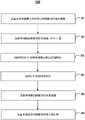
图3A和图3B是根据本公开内容的一些实施例示出用于形成具有抗蚀刻层以降低在半导体插塞中的材料损失的3D存储器件的示例性方法的流程图。3A and 3B are flowcharts illustrating an exemplary method for forming a 3D memory device having an etch resistant layer to reduce material loss in a semiconductor plug, according to some embodiments of the present disclosure.
图4A-4C示出用于根据传统方法来形成沟道结构的示例性制造工艺。4A-4C illustrate exemplary fabrication processes for forming channel structures according to conventional methods.
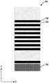
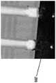
图5A和图5B示出由于蚀刻不足而导致的示例性非晶硅残留物的图像。5A and 5B show images of exemplary amorphous silicon residues due to underetching.
图5C和5D分别示出在核心区域和在虚设区域中的示例性半导体插塞的图像。5C and 5D show images of exemplary semiconductor plugs in the core region and in the dummy region, respectively.
图6A和6B示出由于在半导体插塞中的过多材料损失而导致的示例性短路场景。6A and 6B illustrate exemplary short circuit scenarios due to excessive material loss in a semiconductor plug.
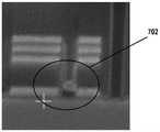
图7A-7C示出示例性短路场景的图像。7A-7C illustrate images of exemplary short circuit scenarios.
将参考附图来描述本公开内容的实施例。Embodiments of the present disclosure will be described with reference to the accompanying drawings.
具体实施方式Detailed ways
虽然讨论了具体的配置和布置,但是应当理解的是,这仅是出于说明性目的来进行的。相关领域技术人员将认识到的是,在不背离本公开内容的精神和保护范围的情况下可以使用其它配置和布置。对于相关领域技术人员来说将显而易见的是,本公开内容还可以是在各种其它应用中采用的。While specific configurations and arrangements are discussed, it should be understood that this is done for illustrative purposes only. Those skilled in the relevant art will recognize that other configurations and arrangements may be used without departing from the spirit and scope of the present disclosure. It will be apparent to those skilled in the relevant art that the present disclosure may also be employed in various other applications.
应当注意的是,说明书中对“一个实施例”、“一实施例”、“示例性实施例”、“一些实施例”等等的提及指示所描述的实施例可以包括特定的特征、结构或特性,但是每个实施例可能不一定包括该特定的特征、结构或特性。此外,这样的短语不一定指的是同一实施例。进一步地,当结合实施例描述特定的特征、结构或特性时,无论是否明确地描述,结合其它实施例来实现这样的特征、结构或特性将在相关领域技术人员的知识范围之内。It should be noted that references in the specification to "one embodiment," "an embodiment," "exemplary embodiment," "some embodiments," etc. indicate that the described embodiment may include the particular feature, structure, etc. or characteristic, but each embodiment may not necessarily include that particular feature, structure, or characteristic. Moreover, such phrases are not necessarily referring to the same embodiment. Further, when a particular feature, structure or characteristic is described in conjunction with one embodiment, whether explicitly described or not, it will be within the knowledge of those skilled in the relevant art to implement such feature, structure or characteristic in conjunction with other embodiments.
通常,可以至少部分地根据在上下文中的使用来理解术语。例如,至少部分地取决于上下文,如本文所使用的术语“一个或多个”可以用于以单数意义来描述任何特征、结构或特性,或者可以用于以复数意义来描述特征、结构或特性的组合。类似地,诸如“一(a)”、“一个(an)”或“该”的术语可以被理解为传达单数用法或者传达复数用法,这至少部分地取决于上下文。另外,术语“基于”可以被理解为不一定旨在传达排他性因素集合,以及可以反而至少部分地取决于上下文再次考虑到存在不一定明确地描述的额外的因素。In general, terms are to be understood at least in part from their use in the context. For example, the term "one or more" as used herein may be used in the singular to describe any feature, structure or characteristic or may be used in the plural to describe the feature, structure or characteristic, depending at least in part on the context The combination. Similarly, terms such as "a", "an" or "the" may be understood to convey singular usage or to convey plural usage, depending at least in part on the context. Additionally, the term "based on" may be understood as not necessarily intended to convey an exclusive set of factors, and may instead take into account that there are additional factors not necessarily explicitly described, again depending at least in part on the context.
应当容易理解的是,本公开内容中的“在……上(on)”、“上方(above)”和“之上(over)”的含义应该以最广泛的方式来解释,使得“在……上”不仅意指“直接在某物上”,而且还包括在其之间具有中间特征或层的“在某物上”的含义,以及“上方”或“之上”不仅意指“在某物上方”或“在某物之上”的含义,而且还可以包括在其之间不具有中间特征或层的“在某物上方”或“在某物之上”的含义(即,直接在某物上)。It should be readily understood that the meanings of "on," "above," and "over" in this disclosure are to be construed in the broadest manner such that "on" On" means not only "directly on something", but also "on something" with intervening features or layers, and "over" or "over" means not only "on" The meaning of "above" or "over something", but can also include "above" or "above" without intervening features or layers (i.e., directly on something).
进一步地,为了便于描述以说明一个元件或特征与另一元件或特征的关系(如图所示),在本文中可以使用诸如“下方(beneath)”、“之下(below)”、“下面(lower)”、“上方”、“上面(upper)”等等的空间相对术语。除了图中所描绘的定向之外,空间相对术语旨在涵盖在使用或操作中的设备的不同定向。装置可以以其它方式来定向(旋转90度或者在其它方向上),以及同样可以相应地解释本文所使用的空间相对描述符。Further, for ease of description to illustrate the relationship of one element or feature to another element or feature (as shown in the figures), expressions such as "beneath", "below", "below" may be used herein. Spatially relative terms such as "lower", "above", "upper", etc. In addition to the orientation depicted in the figures, spatially relative terms are intended to encompass different orientations of the device in use or operation. The device may be otherwise oriented (rotated 90 degrees or at other orientations), and the spatially relative descriptors used herein may likewise be interpreted accordingly.
如本文所使用的,术语“衬底”指的是在其上添加后续材料层的材料。衬底本身可以进行图案化。添加在衬底的顶部的材料可以被图案化或者可以保持未图案化。此外,衬底可以包括各种各样的半导体材料,诸如硅、锗、砷化镓、磷化铟等等。或者,衬底可以由诸如玻璃、塑料或蓝宝石晶圆的非导电材料来制成。As used herein, the term "substrate" refers to the material upon which subsequent layers of material are added. The substrate itself can be patterned. The material added on top of the substrate may be patterned or may remain unpatterned. Additionally, the substrate may include a variety of semiconductor materials such as silicon, germanium, gallium arsenide, indium phosphide, and the like. Alternatively, the substrate can be made of a non-conductive material such as glass, plastic or sapphire wafer.
如本文所使用的,术语“层”指的是包括具有厚度的区域的材料部分。层可以在整个在下面的或在上面的结构之上延伸,或者可以具有小于在下面的或在上面的结构的范围的范围。进一步地,层可以是均匀的或不均匀的连续结构的区域,该不均匀的连续结构具有小于连续结构的厚度的厚度。例如,层可以位于在连续结构的顶表面与底表面之间或者顶表面和底表面处的任何一对水平平面之间。层可以水平地、垂直地和/或沿锥形表面进行延伸。衬底可以是层,可以在其中包括一个或多个层,和/或可以在其上、其之上和/或其之下具有一个或多个层。层可以包含多个层。例如,互连层可以包括一个或多个导体和触点层(在其中形成互连线和/或通孔触点)和一个或多个电介质层。As used herein, the term "layer" refers to a portion of a material that includes a region having a thickness. A layer may extend over the entire underlying or overlying structure, or may have an extent that is less than the extent of the underlying or overlying structure. Further, a layer may be a region of a uniform or non-uniform continuous structure having a thickness that is less than the thickness of the continuous structure. For example, a layer may be located between the top and bottom surfaces of the continuous structure or between any pair of horizontal planes at the top and bottom surfaces. Layers may extend horizontally, vertically and/or along tapered surfaces. The substrate may be a layer, may include one or more layers therein, and/or may have one or more layers thereon, over it, and/or under it. Layers can contain multiple layers. For example, interconnect layers may include one or more conductor and contact layers (in which interconnect lines and/or via contacts are formed) and one or more dielectric layers.
如本文所使用的,术语“标称/名义上”指的是在产品或工艺的设计阶段期间设定的针对组件或工艺操作的特征或参数的期望值或目标值,连同高于和/或低于期望值的一系列值。该值的范围可能是由于在制造工艺或公差的微小变化造成的。如本文所使用的,术语“大约”指示可以基于与主题半导体器件相关联的特定技术节点而变化的给定数量的值。基于特定的技术节点,术语“大约”可以指示在例如值的10-30%内变化的给定数量的值(例如,值的±10%、±20%或±30%)。As used herein, the term "nominal/nominal" refers to an expected or target value for a feature or parameter of a component or process operation set during the design phase of a product or process, along with higher and/or lower A series of values based on the expected value. The range of values may be due to small variations in manufacturing process or tolerances. As used herein, the term "about" indicates a given amount of value that may vary based on the particular technology node associated with the subject semiconductor device. Based on a particular technology node, the term "about" may indicate a given number of values (eg, ±10%, ±20%, or ±30% of the value) that vary, eg, within 10-30% of the value.
如本文所使用的,术语“3D存储器件”指的是在横向地定向的衬底上具有垂直地定向的存储单元晶体管串(在本文中称为“存储串”,诸如NAND存储串)的半导体器件,以便存储串在相对于衬底的垂直方向上延伸。如本文所使用的,术语“垂直/垂直地”意指名义上垂直于衬底的横向表面。As used herein, the term "3D memory device" refers to a semiconductor having vertically oriented strings of memory cell transistors (referred to herein as "strings", such as NAND strings) on a laterally oriented substrate device so that the memory strings extend in a vertical direction relative to the substrate. As used herein, the term "vertical/vertically" means nominally perpendicular to the lateral surface of the substrate.
在一些3D存储器件(诸如3D NAND存储器件)中,通常在NAND存储串的一端形成半导体插塞。当半导体插塞与在其周围形成的栅极导体层组合时,其充当为晶体管的沟道。半导体插塞可以是通过选择性外延生长(SEG)工艺来形成的,在选择性外延生长工艺中半导体插塞是在延伸穿过电介质堆叠的开口中从衬底外延地生长的。通过SEG工艺形成的半导体插塞还称为SEG插塞。In some 3D memory devices, such as 3D NAND memory devices, a semiconductor plug is typically formed at one end of a NAND memory string. When combined with the gate conductor layer formed around the semiconductor plug, it acts as a channel for the transistor. The semiconductor plugs may be formed by selective epitaxial growth (SEG) processes in which the semiconductor plugs are epitaxially grown from the substrate in openings extending through the dielectric stack. The semiconductor plugs formed by the SEG process are also referred to as SEG plugs.
在形成半导体插塞之后,沟道结构可以是在上方的开口中形成的并且与半导体插塞相接触。图4A-4C示出用于形成沟道结构的示例性制造工艺。在图4A-4C中,x轴是平行于晶圆表面的横向方向,而y轴是垂直于晶圆表面的垂直方向。图4A示出衬底402上的电介质堆叠404。电介质堆叠404包括多个交错的电介质层406和牺牲层408。通过在延伸穿过电介质堆叠404的开口410中从衬底402外延地生长来形成半导体插塞412。在半导体插塞412的顶部形成存储膜420。存储膜420包括氧化硅层422、氮化硅层424和另一氧化硅层426(例如,“ONO”结构)。在由存储膜420围绕的空间内部并沿着存储膜420的侧壁形成非晶硅(A-Si)层430。A-Si层430用作保护层以在图4B中所示的干蚀刻或冲压工艺期间保护存储膜420,以及保护随后通过例如湿蚀刻工艺去除的牺牲层。在图4B中,执行蚀刻工艺(例如,干蚀刻工艺)或冲压工艺以形成开口414,该开口414延伸穿过A-Si层430的底部和存储膜420以到达半导体插塞412。在该过程期间可以将A-Si中的一些A-Si蚀刻掉,但是保护存储膜420。在图4C中,执行另一蚀刻工艺(例如,湿蚀刻工艺)以去除A-Si层430的剩余部分。由于在A-Si与半导体插塞412的材料(例如,单晶硅)之间的相对低的选择性,因此在蚀刻工艺中使用的蚀刻溶液(例如,氢氧化铵(NH4OH))可能蚀刻掉过量的半导体插塞412的材料,以便去除所有剩余的A-Si,如通过在图4C中的半导体插塞412内的相对大的孔洞414所示。另一方面,为了限制半导体插塞412的材料的损失,可能存在A-Si残留物,其可能在随后的制造工艺中不利地影响对诸如多晶硅的其它半导体材料的沉积。在半导体插塞412中的过量的A-Si残留物与过量的材料损失之间取得平衡是具有挑战性的。After forming the semiconductor plug, a channel structure may be formed in the overlying opening and in contact with the semiconductor plug. 4A-4C illustrate exemplary fabrication processes for forming channel structures. In Figures 4A-4C, the x-axis is the lateral direction parallel to the wafer surface, and the y-axis is the vertical direction perpendicular to the wafer surface. FIG. 4A shows
图5A和5B示出由于蚀刻不足而导致的示例性A-Si残留物510的图像(顶视图)。这样的A-Si残留物可能存在于存储串所在的核心区域和/或虚设结构所在的虚设区域中,以向3D存储设备提供支撑和平衡。图5C示出在核心区域中的示例性半导体插塞的图像(横截面视图),其中由于在核心区域中的相对小的临界尺寸,因此在半导体插塞502中的材料损失不明显。图5D示出在虚设区域中的示例性半导体插塞的图像(横截面视图),其中由于在虚设区域中的相对大的临界尺寸,因此在半导体插塞502’中的材料损失很大。5A and 5B show images (top view) of an exemplary
在半导体插塞中材料的过多损失可能引起各种问题,诸如在半导体沟道与位于附近的导体层之间的短路。图6A和6B示出这样的示例性短路场景。在图6A和6B中的x-y轴与在图4A-4C中的那些相同。图6A示出在用于去除A-Si的蚀刻工艺期间被蚀刻掉大部分的半导体插塞612,留下了延伸穿过半导体插塞612的侧壁并到达附近的牺牲层608的大开口614。在随后的栅极替换过程期间,将诸如金属的导体材料填充到先前被牺牲层608占据的空间中,以变成导体层609(图6B),从而不可避免地流入开口614并引起短路。图7A-7C是分别地示出在样本存储器件中的示例性短路情况702、704和706的图像。这些短路情况可能引起性能问题或者甚至器件故障。因此,期望减少在去除A-Si的蚀刻工艺期间在半导体插塞中的材料损失,以解决上文讨论的问题。Excessive loss of material in a semiconductor plug can cause various problems, such as short circuits between the semiconductor channel and a nearby conductor layer. 6A and 6B illustrate such exemplary short circuit scenarios. The x-y axes in Figures 6A and 6B are the same as those in Figures 4A-4C. 6A shows that most of the
根据本公开内容的实施例提供了具有抗蚀刻层用于减少在半导体插塞中的材料损失的3D存储器件以及这样的3D存储器件的制造方法。可以在半导体插塞的顶部通过掺杂具有抗蚀刻材料(诸如碳)的部分来形成抗蚀刻层。抗蚀刻层可以防止用于去除A-Si的蚀刻溶液蚀刻穿过该抗蚀刻层,从而在蚀刻工艺期间保持半导体插塞在抗蚀刻层底下的剩余部分的完整性。因此,可以克服由在半导体插塞中的过多材料损失所引起的上文所述的缺点,以及可以改善3D存储器件的产量和可靠性。另外,代替使用硅来形成半导体插塞,可以使用诸如硅锗(SiGe)的具有高载流子迁移率的其它半导体材料来改善载流子迁移率,从而进一步增强3D存储器件的性能。Embodiments in accordance with the present disclosure provide a 3D memory device having an etch-resistant layer for reducing material loss in a semiconductor plug and a method of fabricating such a 3D memory device. An etch-resistant layer may be formed on top of the semiconductor plug by doping a portion with an etch-resistant material, such as carbon. The etch-resistant layer can prevent the etching solution used to remove the A-Si from etching through the etch-resistant layer, thereby maintaining the integrity of the remaining portion of the semiconductor plug under the etch-resistant layer during the etching process. Therefore, the above-mentioned disadvantages caused by excessive material loss in the semiconductor plug can be overcome, and the yield and reliability of the 3D memory device can be improved. In addition, instead of using silicon to form semiconductor plugs, other semiconductor materials with high carrier mobility, such as silicon germanium (SiGe), can be used to improve carrier mobility, thereby further enhancing the performance of 3D memory devices.
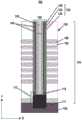
图1根据本公开内容的一些实施例示出具有抗蚀刻层用于减少在半导体插塞中的材料损失的示例性3D存储器件100。如在图1中所示,存储器件100可以包括衬底102和单元堆叠103。衬底102可以包括硅或者其它适当的半导体材料。单元堆叠103可以包括存储堆叠105和存储串160。存储堆叠105可以设置在衬底102上并且包括多个交错的导体层109和电介质层106。导体层109可以包括导电材料,所述导电材料包括但不限于W、Co、Cu、Al、多晶硅、硅化物或者其任何组合。电介质层106可以包括诸如氧化硅的电介质材料。1 illustrates an exemplary
应当注意的是,在图1中包括x轴和y轴,以进一步说明在3D存储器件100中的组件的空间关系。衬底102包括在x方向(即,横向方向)上横向地延伸的两个侧表面(例如,顶表面和底表面)。如本文所使用的,当衬底在y方向上位于半导体器件的最低平面中时,确定一个组件(例如,层或器件)是半导体器件的另一组件(例如,层或器件)“上”、“上方”还是“之下”是在y方向(即,垂直方向)上相对于半导体器件的衬底(例如,衬底102)来确定的。用于描述空间关系的相同概念是贯穿本公开内容来应用的。It should be noted that the x-axis and the y-axis are included in FIG. 1 to further illustrate the spatial relationship of the components in the
存储串160可以垂直地延伸穿过存储堆叠105并且与衬底102相接触。在一些实施例中,存储串160可以通过延伸到衬底102中与衬底102相接触,如在图1中所示意性示出的。在一些实施例中,存储串160可以在衬底102的顶表面处与衬底102相接触。存储串160可以包括在存储串的底部的半导体插塞112。半导体插塞112可以是存储串160的通过延伸到衬底102中或者到达衬底102的顶表面来与衬底102相接触的一部分,如上所述。半导体插塞112可以包括两个部分。顶部116可以掺杂有抗蚀刻材料(还称为抗蚀刻层116),以减少在蚀刻工艺期间的材料损失。底部部分117可以不掺杂有抗蚀刻材料,但是由于蚀刻溶液不能蚀刻穿过抗蚀刻层116并且因此不能到达底部117,所以顶部117保护底部部分117不被蚀刻掉。Memory strings 160 may extend vertically through
在一些实施例中,半导体插塞112可以是通过SEG工艺形成的SEG插塞。例如,半导体插塞112可以包括硅(例如,单晶硅)或者具有与衬底102的晶体结构匹配的晶体结构的其它半导体材料。在另一示例中,半导体插塞112可以包括硅锗(SiGe),例如,通过将锗添加到外延地生长的硅中以形成SiGe插塞。SiGe插塞可以改善载流子迁移率,从而改善3D存储器件100的性能。抗蚀刻层116可以包括与底部117相同的半导体材料,但是在其中掺杂有一种或多种额外的抗蚀刻材料。例如,抗蚀刻材料可以包括碳。在另一示例中,对抗蚀刻材料的掺杂可能导致抗蚀刻层116具有与A-Si的蚀刻速率慢得多的蚀刻速率,从而在用于去除A-Si的蚀刻工艺期间增加了选择性。例如,在蚀刻工艺期间,A-Si的蚀刻速率可以比抗蚀刻层116的蚀刻速率要高至少30倍。在又一示例中,当使用氢氧化铵(NH4OH)作为蚀刻溶液时,在室温下,抗蚀刻层116的蚀刻速率可以小于每分钟3纳米。可以通过注入工艺将抗蚀刻材料注入到半导体插塞112的顶部中,以形成抗蚀刻层116。In some embodiments, the semiconductor plugs 112 may be SEG plugs formed through an SEG process. For example, the
存储串160可以包括垂直地延伸穿过交错的导体层109和电介质层106的半导体沟道140。如在图1中所示,半导体沟道140可以延伸到抗蚀刻层116中。在一些实施例中,半导体沟道140可以包括多晶硅。在一些实施例中,电介质材料150(例如,氧化硅)可以填充在半导体沟道140中的空间。The memory strings 160 may include
存储串160还可以包括横向地设置在半导体沟道140与交错的导体层109和电介质层106之间的存储膜120。存储膜120可以是复合的电介质层,诸如隧穿层126、存储层124和阻隔层122的组合。在存储膜120中的各层可以包括电介质材料,该电介质材料包括但不限于氧化硅、氮化硅、氧氮化硅或其任何组合。The
在一些实施例中,3D存储器件100可以包括多个存储串100,各存储串100具有相同的结构,如上文结合图1所讨论的。In some embodiments, the
图2A-2I根据本公开内容的实施例示出用于形成3D存储器件100的示例性制造工艺。图3A和图3B是根据本公开内容的一些实施例的用于形成具有抗蚀刻层以降低在半导体插塞中的材料损失的3D存储器件的示例性方法300的流程图。在下文中,将一起描述图2A-2I、3A和图3B。应当理解的是,在图3A和图3B中示出的操作不是穷举的,以及还可以在所示操作中的任何操作之前、之后或之间执行其它操作。进一步地,操作中的一些操作可以是同时地执行的,或者是以与在图3A和图3B中所示的顺序不同的顺序来执行的。2A-2I illustrate exemplary fabrication processes for forming
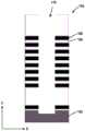
参见图3A,方法300开始于操作310,其中在操作310中,在衬底上形成电介质堆叠。电介质堆叠可以包括多个交错的电介质层和牺牲层。如在图2A中所示,在衬底102上形成包括交错的第一电介质层106和第二电介质层(称为“牺牲层”)108的电介质堆叠104。电介质层106和牺牲层108可以交替地沉积在衬底102上,以形成电介质堆叠104。在一些实施例中,各电介质层106包括氧化硅层,以及各牺牲层108包括氮化硅层。可以通过包括但不限于以下各项的一种或多种薄膜沉积工艺来形成电介质堆叠:化学气相沉积(CVD)、物理气相沉积(PVD)、原子层沉积(ALD)或者其任意组合。衬底102可以包括硅(例如,单晶硅)、硅锗(SiGe)、砷化镓(GaAs)、锗(Ge)、绝缘体上硅(SOI)、绝缘体上锗(GOI)或者任何其它适当的材料。在一些实施例中,衬底102是变薄的衬底(例如,半导体层),其是通过研磨、湿/干蚀刻、化学机械抛光(CMP)或者其任意组合来变薄的。Referring to Figure 3A,
如在图3A中所示,方法300进行到操作320,其中在操作320中,形成垂直地延伸穿过电介质堆叠的开口。如在图2B中所示,形成垂直地延伸穿过电介质堆叠104的开口110(沟道孔)。在一些实施例中,形成穿过电介质堆叠104的多个开口110,使得各开口110变成用于在后续工艺中形成单独的存储串的位置。在一些实施例中,形成开口110的制造工艺包括湿蚀刻和/或干蚀刻,诸如深离子反应蚀刻(DRIE)。如在图2B中所示,蚀刻工艺可以继续进行穿过电介质堆叠104直到到达衬底102。例如,开口110可以延伸到衬底102中。在另一示例中,可以在到达衬底102之前停止蚀刻工艺,以及可以执行后续的冲压工艺以进一步将开口110延伸到衬底102。As shown in FIG. 3A,
返回参考图3A,方法300进行到操作330,其中在操作330中,在开口的下部形成半导体插塞。例如,半导体插塞可以是通过选择性外延生长工艺来形成的SEG插塞,在其中半导体层是在开口中从衬底外延地生长的。如在图2C中所示,可以通过利用从衬底102外延地生长的半导体材料(诸如硅或硅锗(SiGe))填充开口110的下部来形成半导体插塞112(例如,SEG插塞)。用于外延地生长半导体插塞112的制造工艺可以包括但不限于:气相外延(VPE)、液相外延(LPE)、分子束外延(MPE)或者其任意组合。Referring back to FIG. 3A, the
在一些实施例中,用于形成半导体插塞112的半导体材料可以包括SiGe。例如,当温度降低到约800摄氏度时,可以在外延生长工艺期间将锗添加到硅中。使用SiGe作为半导体插塞112的半导体材料,可以增加载流子(例如,电子)迁移率,从而增强3D存储器件的性能。In some embodiments, the semiconductor material used to form the
返回参考图3A,方法300进行到操作340,其中在操作340中,在半导体插塞的顶部形成抗蚀刻层。返回参考图2C,半导体插塞112的顶部116可以掺杂有抗蚀刻材料(诸如碳)以形成抗蚀刻层116。碳可以提供张应力,使得在半导体插塞112的掺杂部分中的应变。应变部分因此可以比硅或SiGe更好地禁得起蚀刻,降低在抗蚀刻层116处的蚀刻速率。在一些实施例中,部分116可以是通过注入工艺利用抗蚀刻材料来掺杂的。例如,可以将碳注入到部分116中以形成抗蚀刻层。Referring back to FIG. 3A, the
如在图3A中所示,方法300进行到操作350,其中在操作350中,形成与在开口中的半导体插塞的抗蚀刻层相接触的沟道结构。在一些实施例中,沟道结构可以包括存储膜和半导体沟道。可以沿着在半导体插塞上方的开口的侧壁来形成存储膜。可以在由存储膜所围绕的空间内形成半导体沟道,沿着存储膜的侧壁垂直地延伸。As shown in FIG. 3A,
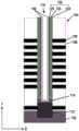
操作350可以包括多个子操作,示出为在图3B中的子操作351-356。参考图3B,操作350从子操作351开始,其中在子操作351中,沿着在半导体插塞上方的开口的侧壁形成存储膜。如在图2D中所示,形成沟道结构的制造工艺可以包括:形成沿着在半导体插塞112上方(例如,在抗蚀刻层116上方)的开口110的侧壁沉积的存储膜120。存储膜120可以是复合的电介质层,诸如隧穿层126、存储层124和阻隔层122的组合。在存储膜120中的各层可以包括电介质材料,该电介质材料包括但不限于氧化硅、氮化硅、氧氮化硅或其任何组合。可以通过一种或多种薄膜沉积工艺(诸如ALD、CVD、PVD、任何其它适当的工艺或者其任意组合)来形成存储膜120。
返回参考图3B,操作350进行到子操作352,其中在子操作352中,沿着存储膜的侧壁沉积非晶硅(A-Si)层。如在图2D中所示,在存储膜120之上并沿着存储膜120的侧壁形成A-Si层130。A-Si层130可以在后续的工艺中起保护层的作用,以保护存储膜不被蚀刻掉,以及可以在形成半导体沟道之前被去除(“牺牲”)。因此,A-Si层130还称为保护层和/或牺牲A-Si层。Referring back to FIG. 3B,
返回参考图3B,操作350进行到子操作353,其中在子操作353中,执行蚀刻工艺以蚀刻穿过A-Si层和存储膜以到达抗蚀刻层。如在图2E中所示,通过蚀刻工艺形成开口114。开口114延伸穿过A-Si层130的底部和存储膜120,以及暴露抗蚀刻层116。在一些实施例中,可以执行干蚀刻工艺以形成开口114。在蚀刻工艺期间,还可以去除沉积在存储膜120的侧壁上的A-Si层130的一部分。Referring back to FIG. 3B,
返回参考图3B,操作350进行到子操作354,其中在子操作354中,去除A-Si层的剩余部分。如在图2F中所示,可以通过湿蚀刻工艺来去除A-Si层130的剩余部分。例如,可以使用诸如氢氧化铵(NH4OH)的蚀刻溶液来去除A-Si。在该蚀刻工艺期间,抗蚀刻层116可以禁得起蚀刻,使得在抗蚀刻层中未发生显著的材料损失。例如,在蚀刻工艺期间,A-Si层的剩余部分的蚀刻速率可以比抗蚀刻层116的蚀刻速率要高至少30倍。在另一示例中,当将NH4OH用作蚀刻溶液时,在蚀刻工艺期间,在室温下,抗蚀刻层116的蚀刻速率小于每分钟3纳米。应当注意的是,可以使用任何材料用于在半导体插塞112中进行掺杂以形成抗蚀刻层116,只要作为结果的抗蚀刻层的蚀刻速率显著地低于A-Si的蚀刻速率(例如,在室温下,相对于NH4OH至少慢30倍或者小于每分钟3纳米)。抗蚀刻层116可以防止蚀刻工艺蚀刻穿过抗蚀刻层,从而防止在半导体插塞112中的显著的材料损失。Referring back to FIG. 3B,
返回参考图3B,操作350进行到子操作355,其中在子操作355中,沿着存储膜的侧壁沉积多晶硅层以形成半导体沟道。如在图2G中所示,可以在存储膜120的侧壁之上并沿着存储膜120的侧壁来沉积多晶硅层140。多晶硅层140可以到达抗蚀刻层116、半导体插塞112的顶部。在一些实施例中,多晶硅层140可以延伸到抗蚀刻层116,但是不穿过抗蚀刻层116到达半导体插塞112的下部(例如,未掺杂有抗蚀刻材料的部分)。多晶硅层140可以形成半导体沟道,作为延伸穿过电介质堆叠104的存储串的一部分。Referring back to FIG. 3B,
返回参考图3B,操作350进行到子操作356,其中在子操作356中,沿着多晶硅层的侧壁沉积电介质材料(例如,氧化硅)。如在图2H中所示,可以沉积电介质材料150以填充开口110的剩余空间(例如,在图2G中所示)。电介质材料150可以用作支撑结构以支撑存储串以及改善稳定性。Referring back to FIG. 3B,
返回参考图3A,方法300进行到操作360,其中在操作360中,通过利用导体层代替在电介质堆叠中的牺牲层来形成存储堆叠。因此,存储堆叠可以包括交错的导体层和电介质层。在一些实施例中,为了形成存储堆叠,形成穿过电介质堆叠的缝隙,穿过该缝隙来蚀刻在电介质堆叠中的牺牲层以形成多个横向凹槽,沿着该缝隙的侧壁和横向凹槽来沉积栅极电介质层,以及在栅极电介质层之上沉积导体层。Referring back to FIG. 3A, the
如在图2I中所示,通过导体层109来替换牺牲层108。结果,可以形成存储堆叠105。导体层109可以包括导电材料,该导电材料包括但不限于W、Co、Cu、Al、多晶硅、硅化物或者其任何组合。存储膜120(例如,在图2H中)和半导体沟道(例如,在图2H中包括多晶硅层140和电介质材料150)共同地形成存储串160。存储串160和存储堆叠105可以形成作为3D存储器件100(其可以是NAND闪存器件)的存储单元的单元堆叠103。As shown in FIG. 2I , the
在一些实施例中,单元堆叠103可以是单片3D存储器件的一部分。术语“单片”意指在单个衬底上形成3D存储器件的组件(例如,外围器件和存储阵列器件)。对于单片3D存储器件,由于外围器件处理和存储阵列器件处理的回旋(convolution),制造将遇到额外的限制。例如,对存储阵列器件(例如,NAND存储串)的制造受到与已经形成在同一衬底上或者将要形成在同一衬底上的外围器件相关联的热预算的约束。In some embodiments,
或者,单元堆叠103可以是非单片3D存储器件的一部分,在其中可以分别在不同的衬底上形成组件(例如,外围器件和存储阵列器件),然后例如以面对面的方式进行键合。在一些实施例中,存储阵列器件衬底(例如,衬底102)保持为键合的非单片3D存储器件的衬底,以及对外围器件(例如,用于促进单元堆叠103的操作的任何适当的数字、模拟和/或混合信号外围电路,诸如页缓冲器、解码器和锁存器;未示出)进行翻转并且向下面向存储阵列器件(例如,NAND存储串)用于进行混合键合。应当理解的是,在一些实施例中,对存储阵列器件衬底(例如,衬底102)进行翻转并且向下面向外围器件(未示出)用于进行混合键合,以便在键合的非单片3D存储器件中,存储阵列器件位于外围器件上方。存储阵列器件衬底(例如,衬底102)可以是变薄的衬底(其不是键合的非单片3D存储器件的衬底),以及可以在变薄的存储阵列器件衬底的背面上形成非单片3D存储器件的后段制程(BEOL)互连。Alternatively,
应该理解的是,用于减少在半导体插塞中的材料损失的抗蚀刻层的应用并不仅仅限于3D存储器件。更通用的器件可以是具有半导体插塞的任何半导体结构。It should be understood that the application of etch-resistant layers for reducing material loss in semiconductor plugs is not limited to 3D memory devices. A more general device can be any semiconductor structure with a semiconductor plug.
根据本公开内容的一方面,提供了一种3D存储器件。该存储器件包括衬底、以及设置在所述衬底上的存储堆叠。所述存储堆叠包括多个交错的导体层和电介质层。该存储器件还包括多个存储串,各存储串垂直地延伸穿过所述存储堆叠并且在所述存储串的底部包括半导体插塞。所述半导体插塞与所述衬底相接触并且包括掺杂有抗蚀刻材料的顶部。According to an aspect of the present disclosure, a 3D memory device is provided. The memory device includes a substrate, and a memory stack disposed on the substrate. The memory stack includes a plurality of interleaved conductor and dielectric layers. The memory device also includes a plurality of memory strings, each memory string extending vertically through the memory stack and including a semiconductor plug at the bottom of the memory string. The semiconductor plug is in contact with the substrate and includes a top doped with an etch-resistant material.
在一些实施例中,所述半导体插塞是选择性外延生长(SEG)插塞。In some embodiments, the semiconductor plugs are selective epitaxial growth (SEG) plugs.
在一些实施例中,所述半导体插塞包括硅锗(SiGe)。In some embodiments, the semiconductor plug includes silicon germanium (SiGe).
在一些实施例中,所述半导体插塞包括硅。In some embodiments, the semiconductor plug includes silicon.
在一些实施例中,所述抗蚀刻材料包括碳。In some embodiments, the etch-resistant material includes carbon.
在一些实施例中,在蚀刻工艺期间,非晶硅(A-Si)的蚀刻速率比掺杂有所述抗蚀刻材料的所述顶部的蚀刻速率要高至少30倍。In some embodiments, the etch rate of amorphous silicon (A-Si) is at least 30 times higher than the etch rate of the top portion doped with the etch resistant material during the etch process.
在一些实施例中,在使用氢氧化铵(NH4OH)作为蚀刻溶液的蚀刻工艺期间,掺杂有所述抗蚀刻材料的所述顶部的蚀刻速率小于每分钟3纳米。In some embodiments, the etch rate of the top portion doped with the etch resistant material is less than 3 nanometers per minute during an etch process using ammonium hydroxide (NH4 OH) as an etch solution.
在一些实施例中,所述抗蚀刻材料被注入到所述半导体插塞的所述顶部中。In some embodiments, the etch resistant material is implanted into the top of the semiconductor plug.
在一些实施例中,所述存储串中的各存储串还包括:垂直地穿过所述交错的导体层和电介质层的半导体沟道。In some embodiments, each of the memory strings further includes a semiconductor channel vertically passing through the interleaved conductor and dielectric layers.
在一些实施例中,所述存储串中的各存储串还包括:在所述半导体沟道与所述交错的导体层和电介质层之间横向地设置的存储膜。In some embodiments, each of the memory strings further includes: a memory film disposed laterally between the semiconductor channel and the interleaved conductor and dielectric layers.
根据本公开内容的另一方面,公开了一种用于形成3D存储器件的方法。该方法包括:在衬底上形成电介质堆叠。所述电介质堆叠包括多个交错的电介质层和牺牲层。该方法还包括:形成垂直地延伸穿过所述电介质堆叠以到达所述衬底的开口。该方法还包括:在所述开口的下部形成半导体插塞。所述半导体插塞与所述衬底相接触。该方法还包括:在所述半导体插塞的顶部形成抗蚀刻层。此外,该方法包括:在所述开口中形成沟道结构。所述沟道结构与所述半导体插塞的所述抗蚀刻层相接触。此外,该方法包括:通过利用所述导体层替换在所述电介质堆叠中的所述牺牲层,来形成包括多个交错的电介质层和导体层的存储堆叠。According to another aspect of the present disclosure, a method for forming a 3D memory device is disclosed. The method includes forming a dielectric stack on a substrate. The dielectric stack includes a plurality of interleaved dielectric layers and sacrificial layers. The method also includes forming an opening extending vertically through the dielectric stack to reach the substrate. The method also includes forming a semiconductor plug in a lower portion of the opening. The semiconductor plug is in contact with the substrate. The method also includes forming an etch-resistant layer on top of the semiconductor plug. Additionally, the method includes forming a channel structure in the opening. The channel structure is in contact with the etch resistant layer of the semiconductor plug. Additionally, the method includes forming a memory stack including a plurality of interleaved dielectric and conductor layers by replacing the sacrificial layer in the dielectric stack with the conductor layer.
在一些实施例中,为了形成所述半导体插塞,半导体层是在所述开口中从所述衬底外延地生长的。In some embodiments, to form the semiconductor plug, a semiconductor layer is epitaxially grown from the substrate in the opening.
在一些实施例中,所述半导体层包括硅。In some embodiments, the semiconductor layer includes silicon.
在一些实施例中,所述半导体层包括硅锗(SiGe)。In some embodiments, the semiconductor layer includes silicon germanium (SiGe).
在一些实施例中,为了形成所述抗蚀刻层,碳被注入到所述半导体插塞的所述顶部中。In some embodiments, to form the etch resistant layer, carbon is implanted into the top of the semiconductor plug.
在一些实施例中,为了形成所述沟道结构,存储膜是沿着在所述半导体插塞上方的所述开口的侧壁来形成的。In some embodiments, to form the channel structure, a storage film is formed along sidewalls of the opening over the semiconductor plug.
在一些实施例中,为了形成所述沟道结构,非晶硅(A-Si)层是沿着所述存储膜的侧壁来沉积的。In some embodiments, to form the channel structure, an amorphous silicon (A-Si) layer is deposited along sidewalls of the memory film.
在一些实施例中,为了形成所述沟道结构,所述A-Si层和所述存储膜被蚀刻穿过以到达所述半导体插塞的所述抗蚀刻层。In some embodiments, to form the channel structure, the A-Si layer and the storage film are etched through to reach the etch resistant layer of the semiconductor plug.
在一些实施例中,为了形成所述沟道结构,所述A-Si层的剩余部分是通过蚀刻工艺来去除的。In some embodiments, to form the channel structure, the remaining portion of the A-Si layer is removed by an etching process.
在一些实施例中,在所述蚀刻工艺期间,所述A-Si层的所述剩余部分的蚀刻速率比所述抗蚀刻层的蚀刻速率要高至少30倍。In some embodiments, the etch rate of the remaining portion of the A-Si layer is at least 30 times higher than the etch rate of the etch resistant layer during the etch process.
在一些实施例中,所述蚀刻工艺是使用氢氧化铵(NH4OH)来执行的,以及在所述蚀刻工艺期间,所述抗蚀刻层的蚀刻速率小于每分钟3纳米。In some embodiments, the etch process is performed using ammonium hydroxide (NH4 OH), and the etch rate of the etch resistant layer is less than 3 nanometers per minute during the etch process.
在一些实施例中,所述抗蚀刻层防止所述蚀刻工艺蚀刻穿过所述抗蚀刻层。In some embodiments, the etch-resistant layer prevents the etching process from etching through the etch-resistant layer.
在一些实施例中,为了形成所述沟道结构,多晶硅层是在去除所述A-Si层的所述剩余部分之后沿着所述存储膜的所述侧壁沉积的。In some embodiments, to form the channel structure, a polysilicon layer is deposited along the sidewalls of the memory film after removing the remaining portion of the A-Si layer.
在一些实施例中,所述多晶硅层延伸到所述抗蚀刻层中。In some embodiments, the polysilicon layer extends into the etch resistant layer.
在一些实施例中,为了形成所述沟道结构,电介质材料是沿着所述多晶硅层的侧壁来沉积的。In some embodiments, to form the channel structure, a dielectric material is deposited along sidewalls of the polysilicon layer.
在一些实施例中,所述衬底包括硅,以及所述牺牲层包括氮化硅。In some embodiments, the substrate includes silicon, and the sacrificial layer includes silicon nitride.
根据本公开内容的另一方面,提供了一种用于形成半导体结构的方法。该方法包括:在衬底上形成多个交错的电介质层和牺牲层。该方法还包括:形成垂直地延伸穿过所述交错的电介质层和牺牲层的开口。该方法还包括:在所述开口的下部形成半导体插塞。所述半导体插塞与所述衬底相接触。此外,该方法还包括:利用抗蚀刻材料来掺杂所述半导体插塞的顶部。此外,该方法还包括:在所述开口中形成沟道结构。所述沟道结构延伸到所述半导体插塞的所述顶部。According to another aspect of the present disclosure, a method for forming a semiconductor structure is provided. The method includes forming a plurality of interleaved dielectric layers and sacrificial layers on a substrate. The method also includes forming openings extending vertically through the interleaved dielectric layers and sacrificial layers. The method also includes forming a semiconductor plug in a lower portion of the opening. The semiconductor plug is in contact with the substrate. Additionally, the method includes doping the top of the semiconductor plug with an etch-resistant material. Additionally, the method further includes forming a channel structure in the opening. The channel structure extends to the top of the semiconductor plug.
在一些实施例中,为了形成所述半导体插塞,半导体层是在所述开口中从所述衬底外延地生长的。In some embodiments, to form the semiconductor plug, a semiconductor layer is epitaxially grown from the substrate in the opening.
在一些实施例中,所述半导体层包括硅。In some embodiments, the semiconductor layer includes silicon.
在一些实施例中,所述半导体层包括硅锗(SiGe)。In some embodiments, the semiconductor layer includes silicon germanium (SiGe).
在一些实施例中,所述抗蚀刻材料包括碳。In some embodiments, the etch-resistant material includes carbon.
在一些实施例中,为了掺杂所述半导体插塞的所述顶部,碳被注入到所述半导体插塞的所述顶部中。In some embodiments, carbon is implanted into the top of the semiconductor plug in order to dope the top of the semiconductor plug.
在一些实施例中,为了形成所述沟道结构,存储膜是沿着在所述半导体插塞上方的所述开口的侧壁来形成的。In some embodiments, to form the channel structure, a storage film is formed along sidewalls of the opening over the semiconductor plug.
在一些实施例中,为了形成所述沟道结构,非晶硅(A-Si)层是沿着所述存储膜的侧壁来沉积的。In some embodiments, to form the channel structure, an amorphous silicon (A-Si) layer is deposited along sidewalls of the memory film.
在一些实施例中,为了形成所述沟道结构,所述A-Si层和所述存储膜被蚀刻穿过以到达掺杂有所述抗蚀刻材料的所述半导体插塞的所述顶部。In some embodiments, to form the channel structure, the A-Si layer and the storage film are etched through to reach the top of the semiconductor plug doped with the etch resistant material.
在一些实施例中,为了形成所述沟道结构,所述A-Si层的剩余部分是通过蚀刻工艺来去除的。In some embodiments, to form the channel structure, the remaining portion of the A-Si layer is removed by an etching process.
在一些实施例中,在所述蚀刻工艺期间,所述A-Si的所述剩余部分的蚀刻速率比掺杂有所述抗蚀刻材料的所述半导体插塞的所述顶部的蚀刻速率要高至少30倍。In some embodiments, the remaining portion of the A-Si etch rate is higher than the etch rate of the top portion of the semiconductor plug doped with the etch resistant material during the etch process At least 30 times.
在一些实施例中,所述蚀刻工艺是使用氢氧化铵(NH4OH)来执行的,以及在所述蚀刻工艺期间,掺杂有所述抗蚀刻材料的所述半导体插塞的所述顶部的蚀刻速率小于每分钟3纳米。In some embodiments, the etch process is performed using ammonium hydroxide (NH4 OH), and during the etch process, the top of the semiconductor plug is doped with the etch resistant material The etch rate is less than 3 nanometers per minute.
在一些实施例中,掺杂有所述抗蚀刻材料的所述半导体插塞的所述顶部防止所述蚀刻工艺经由那里进行蚀刻。In some embodiments, the top of the semiconductor plug doped with the etch resistant material prevents the etch process from etching therethrough.
在一些实施例中,为了形成所述沟道结构,多晶硅层是在去除所述A-Si层的所述剩余部分之后沿着所述存储膜的所述侧壁来沉积的。In some embodiments, to form the channel structure, a polysilicon layer is deposited along the sidewalls of the memory film after removing the remaining portion of the A-Si layer.
在一些实施例中,为了形成所述沟道结构,电介质材料是沿着所述多晶硅层的侧壁来沉积的。In some embodiments, to form the channel structure, a dielectric material is deposited along sidewalls of the polysilicon layer.
在一些实施例中,所述衬底包括硅,以及所述牺牲层包括氮化硅。In some embodiments, the substrate includes silicon, and the sacrificial layer includes silicon nitride.
在一些实施例中,为了形成存储堆叠,多个交错的电介质层和导体层是通过利用所述导体层替换所述牺牲层来形成的。In some embodiments, to form a memory stack, a plurality of interleaved dielectric and conductor layers are formed by replacing the sacrificial layers with the conductor layers.
前述对特定实施例的描述将如此揭示本公开内容的一般性质,即在不背离本公开内容的一般概念的情况下,本领域技术人员可以通过应用本领域技术范围内的知识容易地针对这样的特定实施例的各种应用进行修改和/或调整,而无需过度的实验。因此,基于本文给出的教导和指导,这样的调整和修改旨在落入所公开实施例的等效物的含义和范围内。应当理解的是,本文中的措辞或术语是出于描述的目的而非做出限制,使得本说明书的术语或措辞将由本领域熟练技术人员根据教导和指导来解释。The foregoing descriptions of specific embodiments will reveal the general nature of the disclosure in such a way that those skilled in the art can readily address such Various applications of specific embodiments can be modified and/or adjusted without undue experimentation. Therefore, such adaptations and modifications are intended to fall within the meaning and range of equivalents of the disclosed embodiments, based on the teaching and guidance presented herein. It is to be understood that the phraseology or terminology herein is for the purpose of description and not limitation, so that the terms or phraseology of this specification will be interpreted by one skilled in the art based on the teaching and guidance.
上文借助于用于示出特定功能的实现方式以及其关系的功能构建块,来描述了本公开内容的实施例。为了便于描述,本文已经任意定义这些功能构建块的边界。可以定义替代的边界,只要能适当地执行指定的功能以及其关系即可。Embodiments of the present disclosure have been described above with the aid of functional building blocks that illustrate the implementation of specific functions and relationships thereof. The boundaries of these functional building blocks have been arbitrarily defined herein for ease of description. Alternate boundaries may be defined so long as the specified functions and relationships thereof are appropriately performed.
发明内容和摘要部分可以阐述发明人所预期的本公开内容的一个或多个但不是所有示例性实施例,因此其并不是旨在以任何方式对本公开内容和所附权利要求进行限定。The Summary and Abstract sections may set forth one or more, but not all, exemplary embodiments of the disclosure contemplated by the inventors and are therefore not intended to limit the disclosure and the appended claims in any way.
本公开内容的广度和范围不应被上文描述的示例性实施例中的任何示例性实施例所限制,而应当仅根据所附权利要求及其等效物来限定。The breadth and scope of the present disclosure should not be limited by any of the above-described exemplary embodiments, but should be defined only in accordance with the appended claims and their equivalents.
Claims (41)
Applications Claiming Priority (1)
| Application Number | Priority Date | Filing Date | Title |
|---|---|---|---|
| PCT/CN2020/074601WO2021159228A1 (en) | 2020-02-10 | 2020-02-10 | Semiconductor plug having etch-resistant layer in three-dimensional memory devices |
Publications (2)
| Publication Number | Publication Date |
|---|---|
| CN111328428Atrue CN111328428A (en) | 2020-06-23 |
| CN111328428B CN111328428B (en) | 2021-05-25 |
Family
ID=71173592
Family Applications (1)
| Application Number | Title | Priority Date | Filing Date |
|---|---|---|---|
| CN202080000240.5AActiveCN111328428B (en) | 2020-02-10 | 2020-02-10 | Semiconductor plugs with etch-resistant layers in three-dimensional memory devices |
Country Status (4)
| Country | Link |
|---|---|
| US (1) | US11094703B1 (en) |
| CN (1) | CN111328428B (en) |
| TW (1) | TWI749500B (en) |
| WO (1) | WO2021159228A1 (en) |
Cited By (1)
| Publication number | Priority date | Publication date | Assignee | Title |
|---|---|---|---|---|
| CN114582958A (en)* | 2022-04-29 | 2022-06-03 | 长鑫存储技术有限公司 | Manufacturing method of semiconductor structure and semiconductor structure |
Families Citing this family (1)
| Publication number | Priority date | Publication date | Assignee | Title |
|---|---|---|---|---|
| JP2023002045A (en)* | 2021-06-22 | 2023-01-10 | キオクシア株式会社 | Semiconductor memory device |
Citations (5)
| Publication number | Priority date | Publication date | Assignee | Title |
|---|---|---|---|---|
| US20160293621A1 (en)* | 2015-03-31 | 2016-10-06 | Sandisk Technologies Inc. | Bridge line structure for bit line connection in a three-dimensional semiconductor device |
| US20170229472A1 (en)* | 2016-02-04 | 2017-08-10 | Sandisk Technologies Inc. | Multi-tier replacement memory stack structure integration scheme |
| CN108695336A (en)* | 2017-04-07 | 2018-10-23 | 三星电子株式会社 | Three-dimensional semiconductor memory device and the method for manufacturing it |
| CN109417076A (en)* | 2018-10-09 | 2019-03-01 | 长江存储科技有限责任公司 | Plug and forming method thereof between storehouse in three-dimensional storage part |
| CN109417074A (en)* | 2018-09-27 | 2019-03-01 | 长江存储科技有限责任公司 | Semiconductor plug protected by protective dielectric layer in three-dimensional memory device and method of forming the same |
Family Cites Families (8)
| Publication number | Priority date | Publication date | Assignee | Title |
|---|---|---|---|---|
| WO2015038246A2 (en)* | 2013-09-15 | 2015-03-19 | SanDisk Technologies, Inc. | Method of integrating select gate source and memory hole for three-dimensional non-volatile memory device |
| US9530785B1 (en)* | 2015-07-21 | 2016-12-27 | Sandisk Technologies Llc | Three-dimensional memory devices having a single layer channel and methods of making thereof |
| CN108010835B (en)* | 2016-10-28 | 2020-08-07 | 中芯国际集成电路制造(上海)有限公司 | Semiconductor device, manufacturing method thereof and electronic device |
| JP2019050268A (en)* | 2017-09-08 | 2019-03-28 | 東芝メモリ株式会社 | Storage device |
| KR102533146B1 (en)* | 2017-12-08 | 2023-05-18 | 삼성전자주식회사 | Three-dimensional semiconductor devices and method for fabricating the same |
| KR102588311B1 (en)* | 2018-04-03 | 2023-10-13 | 에스케이하이닉스 주식회사 | Semiconductor device and manufacturing method thereof |
| CN109496355B (en)* | 2018-10-23 | 2020-03-27 | 长江存储科技有限责任公司 | Three-dimensional memory device with semiconductor plug formed using backside substrate thinning |
| CN109979509B (en)* | 2019-03-29 | 2020-05-08 | 长江存储科技有限责任公司 | A three-dimensional memory and its programming operation method |
- 2020
- 2020-02-10WOPCT/CN2020/074601patent/WO2021159228A1/ennot_activeCeased
- 2020-02-10CNCN202080000240.5Apatent/CN111328428B/enactiveActive
- 2020-03-31TWTW109110960Apatent/TWI749500B/enactive
- 2020-04-28USUS16/860,913patent/US11094703B1/enactiveActive
Patent Citations (5)
| Publication number | Priority date | Publication date | Assignee | Title |
|---|---|---|---|---|
| US20160293621A1 (en)* | 2015-03-31 | 2016-10-06 | Sandisk Technologies Inc. | Bridge line structure for bit line connection in a three-dimensional semiconductor device |
| US20170229472A1 (en)* | 2016-02-04 | 2017-08-10 | Sandisk Technologies Inc. | Multi-tier replacement memory stack structure integration scheme |
| CN108695336A (en)* | 2017-04-07 | 2018-10-23 | 三星电子株式会社 | Three-dimensional semiconductor memory device and the method for manufacturing it |
| CN109417074A (en)* | 2018-09-27 | 2019-03-01 | 长江存储科技有限责任公司 | Semiconductor plug protected by protective dielectric layer in three-dimensional memory device and method of forming the same |
| CN109417076A (en)* | 2018-10-09 | 2019-03-01 | 长江存储科技有限责任公司 | Plug and forming method thereof between storehouse in three-dimensional storage part |
Cited By (2)
| Publication number | Priority date | Publication date | Assignee | Title |
|---|---|---|---|---|
| CN114582958A (en)* | 2022-04-29 | 2022-06-03 | 长鑫存储技术有限公司 | Manufacturing method of semiconductor structure and semiconductor structure |
| CN114582958B (en)* | 2022-04-29 | 2022-08-02 | 长鑫存储技术有限公司 | Manufacturing method of semiconductor structure and semiconductor structure |
Also Published As
| Publication number | Publication date |
|---|---|
| US11094703B1 (en) | 2021-08-17 |
| TWI749500B (en) | 2021-12-11 |
| TW202131495A (en) | 2021-08-16 |
| CN111328428B (en) | 2021-05-25 |
| WO2021159228A1 (en) | 2021-08-19 |
| US20210249428A1 (en) | 2021-08-12 |
Similar Documents
| Publication | Publication Date | Title |
|---|---|---|
| CN109496361B (en) | Three-dimensional memory device having zigzag slit structure and method of forming the same | |
| CN110140211B (en) | Three-dimensional memory device and manufacturing method thereof | |
| US11605644B2 (en) | Memory stacks having silicon nitride gate-to-gate dielectric layers and methods for forming the same | |
| CN111244100B (en) | Method for forming structurally enhanced semiconductor plugs in three-dimensional memory devices | |
| CN110520985B (en) | Interconnect structure of three-dimensional memory device | |
| US12029038B2 (en) | Three-dimensional memory device having pocket structure in memory string and method for forming the same | |
| CN109496359B (en) | Method for forming three-dimensional memory device with channel structure using natural oxide layer | |
| KR102148408B1 (en) | 3d cross-bar nonvolatile memory | |
| TWI758018B (en) | Channel structures having protruding portions in three-dimensional memory device and method for forming the same | |
| US11751394B2 (en) | Three-dimensional memory device and method for forming the same | |
| CN112567518B (en) | Channel structure having protruding portion in three-dimensional memory device and method for forming the same | |
| US11925019B2 (en) | Channel structures having protruding portions in three-dimensional memory device and method for forming the same | |
| CN111328428B (en) | Semiconductor plugs with etch-resistant layers in three-dimensional memory devices | |
| US11233066B2 (en) | Three-dimensional memory device and method for forming the same | |
| CN111557049A (en) | Three-dimensional memory device and method of forming the same | |
| CN113228282B (en) | Step annealing process for increasing polysilicon grain size in semiconductor devices | |
| CN111357110A (en) | Method for forming a channel structure in a three-dimensional memory device | |
| US20230197817A1 (en) | Low temperature, high germanium, high boron sige:b pepi with titanium silicide contacts for ultra-low pmos contact resistivity and thermal stability | |
| CN113889484A (en) | Three-dimensional memory and preparation method thereof |
Legal Events
| Date | Code | Title | Description |
|---|---|---|---|
| PB01 | Publication | ||
| PB01 | Publication | ||
| SE01 | Entry into force of request for substantive examination | ||
| SE01 | Entry into force of request for substantive examination | ||
| GR01 | Patent grant | ||
| GR01 | Patent grant |