CN111326479A - Semiconductor device and method for manufacturing semiconductor device - Google Patents
Semiconductor device and method for manufacturing semiconductor deviceDownload PDFInfo
- Publication number
- CN111326479A CN111326479ACN201911301152.4ACN201911301152ACN111326479ACN 111326479 ACN111326479 ACN 111326479ACN 201911301152 ACN201911301152 ACN 201911301152ACN 111326479 ACN111326479 ACN 111326479A
- Authority
- CN
- China
- Prior art keywords
- silicon carbide
- layer
- region
- metal
- carbide substrate
- Prior art date
- Legal status (The legal status is an assumption and is not a legal conclusion. Google has not performed a legal analysis and makes no representation as to the accuracy of the status listed.)
- Granted
Links
- 239000004065semiconductorSubstances0.000titleclaimsabstractdescription200
- 238000000034methodMethods0.000titleclaimsabstractdescription131
- 238000004519manufacturing processMethods0.000titleclaimsabstractdescription7
- HBMJWWWQQXIZIP-UHFFFAOYSA-Nsilicon carbideChemical compound[Si+]#[C-]HBMJWWWQQXIZIP-UHFFFAOYSA-N0.000claimsabstractdescription182
- 229910010271silicon carbideInorganic materials0.000claimsabstractdescription182
- 239000000758substrateSubstances0.000claimsabstractdescription170
- 238000000465mouldingMethods0.000claimsabstractdescription70
- 229910052751metalInorganic materials0.000claimsdescription140
- 239000002184metalSubstances0.000claimsdescription140
- 239000000463materialSubstances0.000claimsdescription76
- 238000001465metallisationMethods0.000claimsdescription46
- 229920000642polymerPolymers0.000claimsdescription8
- 239000004642PolyimideSubstances0.000claimsdescription6
- 229920001721polyimidePolymers0.000claimsdescription6
- 238000000151depositionMethods0.000claimsdescription4
- 238000011049fillingMethods0.000claimsdescription3
- -1polytetrafluoroethylenePolymers0.000claimsdescription3
- 229920001343polytetrafluoroethylenePolymers0.000claimsdescription3
- 239000004810polytetrafluoroethyleneSubstances0.000claimsdescription3
- 239000003822epoxy resinSubstances0.000claimsdescription2
- 238000007747platingMethods0.000claimsdescription2
- 229920000647polyepoxidePolymers0.000claimsdescription2
- 229920002050silicone resinPolymers0.000claims1
- 230000000153supplemental effectEffects0.000claims1
- 239000010410layerSubstances0.000description159
- 235000012431wafersNutrition0.000description88
- 230000008569processEffects0.000description57
- 238000000926separation methodMethods0.000description22
- 230000005855radiationEffects0.000description19
- 239000011521glassSubstances0.000description16
- 239000012790adhesive layerSubstances0.000description14
- 230000000295complement effectEffects0.000description14
- 238000004070electrodepositionMethods0.000description13
- 238000000227grindingMethods0.000description12
- 238000010521absorption reactionMethods0.000description11
- 239000011229interlayerSubstances0.000description11
- 239000012778molding materialSubstances0.000description11
- 230000015572biosynthetic processEffects0.000description10
- 239000002131composite materialSubstances0.000description10
- 150000001875compoundsChemical class0.000description10
- 238000002161passivationMethods0.000description10
- 229910052802copperInorganic materials0.000description9
- 239000010949copperSubstances0.000description9
- XUIMIQQOPSSXEZ-UHFFFAOYSA-NSiliconChemical compound[Si]XUIMIQQOPSSXEZ-UHFFFAOYSA-N0.000description8
- 229910052710siliconInorganic materials0.000description8
- 239000010703siliconSubstances0.000description8
- RYGMFSIKBFXOCR-UHFFFAOYSA-NCopperChemical compound[Cu]RYGMFSIKBFXOCR-UHFFFAOYSA-N0.000description7
- 238000009792diffusion processMethods0.000description7
- 238000004806packaging method and processMethods0.000description7
- 229910052782aluminiumInorganic materials0.000description6
- XAGFODPZIPBFFR-UHFFFAOYSA-NaluminiumChemical compound[Al]XAGFODPZIPBFFR-UHFFFAOYSA-N0.000description6
- 238000011109contaminationMethods0.000description6
- 238000009713electroplatingMethods0.000description6
- 230000009477glass transitionEffects0.000description6
- 239000003292glueSubstances0.000description6
- 239000004593EpoxySubstances0.000description5
- 239000000853adhesiveSubstances0.000description5
- 230000001070adhesive effectEffects0.000description5
- 150000002500ionsChemical class0.000description5
- 229920005989resinPolymers0.000description5
- 239000011347resinSubstances0.000description5
- 238000005245sinteringMethods0.000description5
- OKTJSMMVPCPJKN-UHFFFAOYSA-NCarbonChemical compound[C]OKTJSMMVPCPJKN-UHFFFAOYSA-N0.000description4
- JMASRVWKEDWRBT-UHFFFAOYSA-NGallium nitrideChemical compound[Ga]#NJMASRVWKEDWRBT-UHFFFAOYSA-N0.000description4
- 238000012512characterization methodMethods0.000description4
- 239000013078crystalSubstances0.000description4
- 230000005669field effectEffects0.000description4
- 239000007788liquidSubstances0.000description4
- 229910000679solderInorganic materials0.000description4
- 239000000126substanceSubstances0.000description4
- 230000008646thermal stressEffects0.000description4
- 238000003466weldingMethods0.000description4
- PXHVJJICTQNCMI-UHFFFAOYSA-NNickelChemical compound[Ni]PXHVJJICTQNCMI-UHFFFAOYSA-N0.000description3
- 238000005452bendingMethods0.000description3
- 229910052799carbonInorganic materials0.000description3
- 239000000969carrierSubstances0.000description3
- 239000011248coating agentSubstances0.000description3
- 238000000576coating methodMethods0.000description3
- 239000004020conductorSubstances0.000description3
- 230000002427irreversible effectEffects0.000description3
- 230000008018meltingEffects0.000description3
- 238000002844meltingMethods0.000description3
- 238000012536packaging technologyMethods0.000description3
- 229920001296polysiloxanePolymers0.000description3
- 238000012545processingMethods0.000description3
- 230000002441reversible effectEffects0.000description3
- 239000007787solidSubstances0.000description3
- 230000035882stressEffects0.000description3
- 229910052718tinInorganic materials0.000description3
- IJGRMHOSHXDMSA-UHFFFAOYSA-NAtomic nitrogenChemical compoundN#NIJGRMHOSHXDMSA-UHFFFAOYSA-N0.000description2
- 229910002601GaNInorganic materials0.000description2
- 229910052581Si3N4Inorganic materials0.000description2
- ATJFFYVFTNAWJD-UHFFFAOYSA-NTinChemical compound[Sn]ATJFFYVFTNAWJD-UHFFFAOYSA-N0.000description2
- 229910045601alloyInorganic materials0.000description2
- 239000000956alloySubstances0.000description2
- 210000000746body regionAnatomy0.000description2
- 239000000919ceramicSubstances0.000description2
- 229910010293ceramic materialInorganic materials0.000description2
- 238000003776cleavage reactionMethods0.000description2
- 230000008021depositionEffects0.000description2
- 239000003989dielectric materialSubstances0.000description2
- AJNVQOSZGJRYEI-UHFFFAOYSA-Ndigallium;oxygen(2-)Chemical compound[O-2].[O-2].[O-2].[Ga+3].[Ga+3]AJNVQOSZGJRYEI-UHFFFAOYSA-N0.000description2
- 235000013766direct food additiveNutrition0.000description2
- 238000005530etchingMethods0.000description2
- 239000011888foilSubstances0.000description2
- 230000004927fusionEffects0.000description2
- 239000001257hydrogenSubstances0.000description2
- 229910052739hydrogenInorganic materials0.000description2
- 239000012535impuritySubstances0.000description2
- 239000011147inorganic materialSubstances0.000description2
- 239000012212insulatorSubstances0.000description2
- 230000001678irradiating effectEffects0.000description2
- 238000003698laser cuttingMethods0.000description2
- 229910044991metal oxideInorganic materials0.000description2
- 150000004706metal oxidesChemical class0.000description2
- 239000000203mixtureSubstances0.000description2
- 229910052750molybdenumInorganic materials0.000description2
- 229910052759nickelInorganic materials0.000description2
- 229910052757nitrogenInorganic materials0.000description2
- 239000011368organic materialSubstances0.000description2
- 229920002120photoresistant polymerPolymers0.000description2
- 239000004033plasticSubstances0.000description2
- 229920000636poly(norbornene) polymerPolymers0.000description2
- 229910021420polycrystalline siliconInorganic materials0.000description2
- 229920005591polysiliconPolymers0.000description2
- 238000007639printingMethods0.000description2
- 239000011819refractory materialSubstances0.000description2
- 230000007017scissionEffects0.000description2
- HQVNEWCFYHHQES-UHFFFAOYSA-Nsilicon nitrideChemical compoundN12[Si]34N5[Si]62N3[Si]51N64HQVNEWCFYHHQES-UHFFFAOYSA-N0.000description2
- 229910052709silverInorganic materials0.000description2
- 239000002904solventSubstances0.000description2
- 238000012360testing methodMethods0.000description2
- 238000007669thermal treatmentMethods0.000description2
- VXNZUUAINFGPBY-UHFFFAOYSA-N1-ButeneChemical compoundCCC=CVXNZUUAINFGPBY-UHFFFAOYSA-N0.000description1
- 229910000838Al alloyInorganic materials0.000description1
- PIGFYZPCRLYGLF-UHFFFAOYSA-NAluminum nitrideChemical compound[Al]#NPIGFYZPCRLYGLF-UHFFFAOYSA-N0.000description1
- ZOXJGFHDIHLPTG-UHFFFAOYSA-NBoronChemical compound[B]ZOXJGFHDIHLPTG-UHFFFAOYSA-N0.000description1
- QPLDLSVMHZLSFG-UHFFFAOYSA-NCopper oxideChemical compound[Cu]=OQPLDLSVMHZLSFG-UHFFFAOYSA-N0.000description1
- 239000005751Copper oxideSubstances0.000description1
- 229910005191Ga 2 O 3Inorganic materials0.000description1
- GYHNNYVSQQEPJS-UHFFFAOYSA-NGalliumChemical compound[Ga]GYHNNYVSQQEPJS-UHFFFAOYSA-N0.000description1
- UFHFLCQGNIYNRP-UHFFFAOYSA-NHydrogenChemical group[H][H]UFHFLCQGNIYNRP-UHFFFAOYSA-N0.000description1
- ZOKXTWBITQBERF-UHFFFAOYSA-NMolybdenumChemical compound[Mo]ZOKXTWBITQBERF-UHFFFAOYSA-N0.000description1
- 229910003849O-SiInorganic materials0.000description1
- 229910003872O—SiInorganic materials0.000description1
- OAICVXFJPJFONN-UHFFFAOYSA-NPhosphorusChemical compound[P]OAICVXFJPJFONN-UHFFFAOYSA-N0.000description1
- VYPSYNLAJGMNEJ-UHFFFAOYSA-NSilicium dioxideChemical compoundO=[Si]=OVYPSYNLAJGMNEJ-UHFFFAOYSA-N0.000description1
- 239000004809TeflonSubstances0.000description1
- 229920006362Teflon®Polymers0.000description1
- IWBUYGUPYWKAMK-UHFFFAOYSA-N[AlH3].[N]Chemical compound[AlH3].[N]IWBUYGUPYWKAMK-UHFFFAOYSA-N0.000description1
- 239000002318adhesion promoterSubstances0.000description1
- 239000002390adhesive tapeSubstances0.000description1
- JRBRVDCKNXZZGH-UHFFFAOYSA-Nalumane;copperChemical compound[AlH3].[Cu]JRBRVDCKNXZZGH-UHFFFAOYSA-N0.000description1
- 239000004411aluminiumSubstances0.000description1
- 239000012080ambient airSubstances0.000description1
- 229910021417amorphous siliconInorganic materials0.000description1
- QVGXLLKOCUKJST-UHFFFAOYSA-Natomic oxygenChemical compound[O]QVGXLLKOCUKJST-UHFFFAOYSA-N0.000description1
- WPYMKLBDIGXBTP-UHFFFAOYSA-Nbenzoic acid groupChemical groupC(C1=CC=CC=C1)(=O)OWPYMKLBDIGXBTP-UHFFFAOYSA-N0.000description1
- 229910052790berylliumInorganic materials0.000description1
- ATBAMAFKBVZNFJ-UHFFFAOYSA-Nberyllium atomChemical compound[Be]ATBAMAFKBVZNFJ-UHFFFAOYSA-N0.000description1
- 229910052796boronInorganic materials0.000description1
- IAQRGUVFOMOMEM-UHFFFAOYSA-NbuteneNatural productsCC=CCIAQRGUVFOMOMEM-UHFFFAOYSA-N0.000description1
- 238000005266castingMethods0.000description1
- 238000006243chemical reactionMethods0.000description1
- 230000006835compressionEffects0.000description1
- 238000007906compressionMethods0.000description1
- 238000000748compression mouldingMethods0.000description1
- 230000003750conditioning effectEffects0.000description1
- 239000000470constituentSubstances0.000description1
- 229910000431copper oxideInorganic materials0.000description1
- 238000005336crackingMethods0.000description1
- 238000005520cutting processMethods0.000description1
- 238000010494dissociation reactionMethods0.000description1
- 230000005593dissociationsEffects0.000description1
- 239000002019doping agentChemical group0.000description1
- 230000000694effectsEffects0.000description1
- 230000005670electromagnetic radiationEffects0.000description1
- 230000006870functionEffects0.000description1
- 229910052733galliumInorganic materials0.000description1
- 239000007789gasSubstances0.000description1
- 229910052732germaniumInorganic materials0.000description1
- GNPVGFCGXDBREM-UHFFFAOYSA-Ngermanium atomChemical compound[Ge]GNPVGFCGXDBREM-UHFFFAOYSA-N0.000description1
- 229910052737goldInorganic materials0.000description1
- 229910002804graphiteInorganic materials0.000description1
- 239000010439graphiteSubstances0.000description1
- 239000007943implantSubstances0.000description1
- 229910052738indiumInorganic materials0.000description1
- 238000001746injection mouldingMethods0.000description1
- 229910010272inorganic materialInorganic materials0.000description1
- 230000007774longtermEffects0.000description1
- 239000011159matrix materialSubstances0.000description1
- 150000002739metalsChemical class0.000description1
- 238000012986modificationMethods0.000description1
- 230000004048modificationEffects0.000description1
- 239000011733molybdenumSubstances0.000description1
- RUFLMLWJRZAWLJ-UHFFFAOYSA-Nnickel silicideChemical compound[Ni]=[Si]=[Ni]RUFLMLWJRZAWLJ-UHFFFAOYSA-N0.000description1
- 229910021334nickel silicideInorganic materials0.000description1
- 239000012811non-conductive materialSubstances0.000description1
- TWNQGVIAIRXVLR-UHFFFAOYSA-Noxo(oxoalumanyloxy)alumaneChemical compoundO=[Al]O[Al]=OTWNQGVIAIRXVLR-UHFFFAOYSA-N0.000description1
- 239000001301oxygenSubstances0.000description1
- 229910052760oxygenInorganic materials0.000description1
- 238000012858packaging processMethods0.000description1
- 229910052763palladiumInorganic materials0.000description1
- 239000002245particleSubstances0.000description1
- 238000000059patterningMethods0.000description1
- 230000002093peripheral effectEffects0.000description1
- 229910052698phosphorusInorganic materials0.000description1
- 239000011574phosphorusSubstances0.000description1
- 230000000704physical effectEffects0.000description1
- 238000005498polishingMethods0.000description1
- 238000007517polishing processMethods0.000description1
- 229920001709polysilazanePolymers0.000description1
- 229910021426porous siliconInorganic materials0.000description1
- 230000008707rearrangementEffects0.000description1
- 229910052594sapphireInorganic materials0.000description1
- 239000010980sapphireSubstances0.000description1
- 229910052814silicon oxideInorganic materials0.000description1
- 239000004332silverSubstances0.000description1
- 239000005361soda-lime glassSubstances0.000description1
- 238000007711solidificationMethods0.000description1
- 230000008023solidificationEffects0.000description1
- 238000004544sputter depositionMethods0.000description1
- 230000000930thermomechanical effectEffects0.000description1
- 229910052719titaniumInorganic materials0.000description1
- 238000012546transferMethods0.000description1
- 229910052721tungstenInorganic materials0.000description1
- 238000007740vapor depositionMethods0.000description1
- 238000001039wet etchingMethods0.000description1
Images


Classifications
- H—ELECTRICITY
- H01—ELECTRIC ELEMENTS
- H01L—SEMICONDUCTOR DEVICES NOT COVERED BY CLASS H10
- H01L21/00—Processes or apparatus adapted for the manufacture or treatment of semiconductor or solid state devices or of parts thereof
- H01L21/70—Manufacture or treatment of devices consisting of a plurality of solid state components formed in or on a common substrate or of parts thereof; Manufacture of integrated circuit devices or of parts thereof
- H01L21/77—Manufacture or treatment of devices consisting of a plurality of solid state components or integrated circuits formed in, or on, a common substrate
- H01L21/78—Manufacture or treatment of devices consisting of a plurality of solid state components or integrated circuits formed in, or on, a common substrate with subsequent division of the substrate into plural individual devices
- H—ELECTRICITY
- H01—ELECTRIC ELEMENTS
- H01L—SEMICONDUCTOR DEVICES NOT COVERED BY CLASS H10
- H01L21/00—Processes or apparatus adapted for the manufacture or treatment of semiconductor or solid state devices or of parts thereof
- H01L21/67—Apparatus specially adapted for handling semiconductor or electric solid state devices during manufacture or treatment thereof; Apparatus specially adapted for handling wafers during manufacture or treatment of semiconductor or electric solid state devices or components ; Apparatus not specifically provided for elsewhere
- H01L21/683—Apparatus specially adapted for handling semiconductor or electric solid state devices during manufacture or treatment thereof; Apparatus specially adapted for handling wafers during manufacture or treatment of semiconductor or electric solid state devices or components ; Apparatus not specifically provided for elsewhere for supporting or gripping
- H01L21/6835—Apparatus specially adapted for handling semiconductor or electric solid state devices during manufacture or treatment thereof; Apparatus specially adapted for handling wafers during manufacture or treatment of semiconductor or electric solid state devices or components ; Apparatus not specifically provided for elsewhere for supporting or gripping using temporarily an auxiliary support
- H—ELECTRICITY
- H01—ELECTRIC ELEMENTS
- H01L—SEMICONDUCTOR DEVICES NOT COVERED BY CLASS H10
- H01L21/00—Processes or apparatus adapted for the manufacture or treatment of semiconductor or solid state devices or of parts thereof
- H01L21/02—Manufacture or treatment of semiconductor devices or of parts thereof
- H01L21/02104—Forming layers
- H01L21/02365—Forming inorganic semiconducting materials on a substrate
- H01L21/02367—Substrates
- H01L21/0237—Materials
- H01L21/02373—Group 14 semiconducting materials
- H01L21/02378—Silicon carbide
- H—ELECTRICITY
- H01—ELECTRIC ELEMENTS
- H01L—SEMICONDUCTOR DEVICES NOT COVERED BY CLASS H10
- H01L21/00—Processes or apparatus adapted for the manufacture or treatment of semiconductor or solid state devices or of parts thereof
- H01L21/02—Manufacture or treatment of semiconductor devices or of parts thereof
- H01L21/04—Manufacture or treatment of semiconductor devices or of parts thereof the devices having potential barriers, e.g. a PN junction, depletion layer or carrier concentration layer
- H01L21/18—Manufacture or treatment of semiconductor devices or of parts thereof the devices having potential barriers, e.g. a PN junction, depletion layer or carrier concentration layer the devices having semiconductor bodies comprising elements of Group IV of the Periodic Table or AIIIBV compounds with or without impurities, e.g. doping materials
- H01L21/30—Treatment of semiconductor bodies using processes or apparatus not provided for in groups H01L21/20 - H01L21/26
- H01L21/302—Treatment of semiconductor bodies using processes or apparatus not provided for in groups H01L21/20 - H01L21/26 to change their surface-physical characteristics or shape, e.g. etching, polishing, cutting
- H01L21/304—Mechanical treatment, e.g. grinding, polishing, cutting
- H—ELECTRICITY
- H01—ELECTRIC ELEMENTS
- H01L—SEMICONDUCTOR DEVICES NOT COVERED BY CLASS H10
- H01L21/00—Processes or apparatus adapted for the manufacture or treatment of semiconductor or solid state devices or of parts thereof
- H01L21/02—Manufacture or treatment of semiconductor devices or of parts thereof
- H01L21/04—Manufacture or treatment of semiconductor devices or of parts thereof the devices having potential barriers, e.g. a PN junction, depletion layer or carrier concentration layer
- H01L21/50—Assembly of semiconductor devices using processes or apparatus not provided for in a single one of the groups H01L21/18 - H01L21/326 or H10D48/04 - H10D48/07 e.g. sealing of a cap to a base of a container
- H01L21/56—Encapsulations, e.g. encapsulation layers, coatings
- H01L21/561—Batch processing
- H—ELECTRICITY
- H01—ELECTRIC ELEMENTS
- H01L—SEMICONDUCTOR DEVICES NOT COVERED BY CLASS H10
- H01L21/00—Processes or apparatus adapted for the manufacture or treatment of semiconductor or solid state devices or of parts thereof
- H01L21/02—Manufacture or treatment of semiconductor devices or of parts thereof
- H01L21/04—Manufacture or treatment of semiconductor devices or of parts thereof the devices having potential barriers, e.g. a PN junction, depletion layer or carrier concentration layer
- H01L21/50—Assembly of semiconductor devices using processes or apparatus not provided for in a single one of the groups H01L21/18 - H01L21/326 or H10D48/04 - H10D48/07 e.g. sealing of a cap to a base of a container
- H01L21/56—Encapsulations, e.g. encapsulation layers, coatings
- H01L21/565—Moulds
- H—ELECTRICITY
- H01—ELECTRIC ELEMENTS
- H01L—SEMICONDUCTOR DEVICES NOT COVERED BY CLASS H10
- H01L21/00—Processes or apparatus adapted for the manufacture or treatment of semiconductor or solid state devices or of parts thereof
- H01L21/02—Manufacture or treatment of semiconductor devices or of parts thereof
- H01L21/04—Manufacture or treatment of semiconductor devices or of parts thereof the devices having potential barriers, e.g. a PN junction, depletion layer or carrier concentration layer
- H01L21/50—Assembly of semiconductor devices using processes or apparatus not provided for in a single one of the groups H01L21/18 - H01L21/326 or H10D48/04 - H10D48/07 e.g. sealing of a cap to a base of a container
- H01L21/56—Encapsulations, e.g. encapsulation layers, coatings
- H01L21/568—Temporary substrate used as encapsulation process aid
- H—ELECTRICITY
- H01—ELECTRIC ELEMENTS
- H01L—SEMICONDUCTOR DEVICES NOT COVERED BY CLASS H10
- H01L21/00—Processes or apparatus adapted for the manufacture or treatment of semiconductor or solid state devices or of parts thereof
- H01L21/67—Apparatus specially adapted for handling semiconductor or electric solid state devices during manufacture or treatment thereof; Apparatus specially adapted for handling wafers during manufacture or treatment of semiconductor or electric solid state devices or components ; Apparatus not specifically provided for elsewhere
- H01L21/683—Apparatus specially adapted for handling semiconductor or electric solid state devices during manufacture or treatment thereof; Apparatus specially adapted for handling wafers during manufacture or treatment of semiconductor or electric solid state devices or components ; Apparatus not specifically provided for elsewhere for supporting or gripping
- H01L21/6835—Apparatus specially adapted for handling semiconductor or electric solid state devices during manufacture or treatment thereof; Apparatus specially adapted for handling wafers during manufacture or treatment of semiconductor or electric solid state devices or components ; Apparatus not specifically provided for elsewhere for supporting or gripping using temporarily an auxiliary support
- H01L21/6836—Wafer tapes, e.g. grinding or dicing support tapes
- H—ELECTRICITY
- H01—ELECTRIC ELEMENTS
- H01L—SEMICONDUCTOR DEVICES NOT COVERED BY CLASS H10
- H01L23/00—Details of semiconductor or other solid state devices
- H01L23/28—Encapsulations, e.g. encapsulating layers, coatings, e.g. for protection
- H01L23/31—Encapsulations, e.g. encapsulating layers, coatings, e.g. for protection characterised by the arrangement or shape
- H01L23/3107—Encapsulations, e.g. encapsulating layers, coatings, e.g. for protection characterised by the arrangement or shape the device being completely enclosed
- H01L23/3114—Encapsulations, e.g. encapsulating layers, coatings, e.g. for protection characterised by the arrangement or shape the device being completely enclosed the device being a chip scale package, e.g. CSP
- H—ELECTRICITY
- H01—ELECTRIC ELEMENTS
- H01L—SEMICONDUCTOR DEVICES NOT COVERED BY CLASS H10
- H01L23/00—Details of semiconductor or other solid state devices
- H01L23/28—Encapsulations, e.g. encapsulating layers, coatings, e.g. for protection
- H01L23/31—Encapsulations, e.g. encapsulating layers, coatings, e.g. for protection characterised by the arrangement or shape
- H01L23/3157—Partial encapsulation or coating
- H01L23/3185—Partial encapsulation or coating the coating covering also the sidewalls of the semiconductor body
- H—ELECTRICITY
- H10—SEMICONDUCTOR DEVICES; ELECTRIC SOLID-STATE DEVICES NOT OTHERWISE PROVIDED FOR
- H10D—INORGANIC ELECTRIC SEMICONDUCTOR DEVICES
- H10D62/00—Semiconductor bodies, or regions thereof, of devices having potential barriers
- H10D62/80—Semiconductor bodies, or regions thereof, of devices having potential barriers characterised by the materials
- H10D62/83—Semiconductor bodies, or regions thereof, of devices having potential barriers characterised by the materials being Group IV materials, e.g. B-doped Si or undoped Ge
- H10D62/832—Semiconductor bodies, or regions thereof, of devices having potential barriers characterised by the materials being Group IV materials, e.g. B-doped Si or undoped Ge being Group IV materials comprising two or more elements, e.g. SiGe
- H10D62/8325—Silicon carbide
- H—ELECTRICITY
- H10—SEMICONDUCTOR DEVICES; ELECTRIC SOLID-STATE DEVICES NOT OTHERWISE PROVIDED FOR
- H10D—INORGANIC ELECTRIC SEMICONDUCTOR DEVICES
- H10D64/00—Electrodes of devices having potential barriers
- H10D64/20—Electrodes characterised by their shapes, relative sizes or dispositions
- H—ELECTRICITY
- H10—SEMICONDUCTOR DEVICES; ELECTRIC SOLID-STATE DEVICES NOT OTHERWISE PROVIDED FOR
- H10D—INORGANIC ELECTRIC SEMICONDUCTOR DEVICES
- H10D64/00—Electrodes of devices having potential barriers
- H10D64/20—Electrodes characterised by their shapes, relative sizes or dispositions
- H10D64/23—Electrodes carrying the current to be rectified, amplified, oscillated or switched, e.g. sources, drains, anodes or cathodes
- H10D64/232—Emitter electrodes for IGBTs
- H—ELECTRICITY
- H01—ELECTRIC ELEMENTS
- H01L—SEMICONDUCTOR DEVICES NOT COVERED BY CLASS H10
- H01L2221/00—Processes or apparatus adapted for the manufacture or treatment of semiconductor or solid state devices or of parts thereof covered by H01L21/00
- H01L2221/67—Apparatus for handling semiconductor or electric solid state devices during manufacture or treatment thereof; Apparatus for handling wafers during manufacture or treatment of semiconductor or electric solid state devices or components; Apparatus not specifically provided for elsewhere
- H01L2221/683—Apparatus for handling semiconductor or electric solid state devices during manufacture or treatment thereof; Apparatus for handling wafers during manufacture or treatment of semiconductor or electric solid state devices or components; Apparatus not specifically provided for elsewhere for supporting or gripping
- H01L2221/68304—Apparatus for handling semiconductor or electric solid state devices during manufacture or treatment thereof; Apparatus for handling wafers during manufacture or treatment of semiconductor or electric solid state devices or components; Apparatus not specifically provided for elsewhere for supporting or gripping using temporarily an auxiliary support
- H01L2221/68327—Apparatus for handling semiconductor or electric solid state devices during manufacture or treatment thereof; Apparatus for handling wafers during manufacture or treatment of semiconductor or electric solid state devices or components; Apparatus not specifically provided for elsewhere for supporting or gripping using temporarily an auxiliary support used during dicing or grinding
- H—ELECTRICITY
- H01—ELECTRIC ELEMENTS
- H01L—SEMICONDUCTOR DEVICES NOT COVERED BY CLASS H10
- H01L2221/00—Processes or apparatus adapted for the manufacture or treatment of semiconductor or solid state devices or of parts thereof covered by H01L21/00
- H01L2221/67—Apparatus for handling semiconductor or electric solid state devices during manufacture or treatment thereof; Apparatus for handling wafers during manufacture or treatment of semiconductor or electric solid state devices or components; Apparatus not specifically provided for elsewhere
- H01L2221/683—Apparatus for handling semiconductor or electric solid state devices during manufacture or treatment thereof; Apparatus for handling wafers during manufacture or treatment of semiconductor or electric solid state devices or components; Apparatus not specifically provided for elsewhere for supporting or gripping
- H01L2221/68304—Apparatus for handling semiconductor or electric solid state devices during manufacture or treatment thereof; Apparatus for handling wafers during manufacture or treatment of semiconductor or electric solid state devices or components; Apparatus not specifically provided for elsewhere for supporting or gripping using temporarily an auxiliary support
- H01L2221/6834—Apparatus for handling semiconductor or electric solid state devices during manufacture or treatment thereof; Apparatus for handling wafers during manufacture or treatment of semiconductor or electric solid state devices or components; Apparatus not specifically provided for elsewhere for supporting or gripping using temporarily an auxiliary support used to protect an active side of a device or wafer
- H—ELECTRICITY
- H01—ELECTRIC ELEMENTS
- H01L—SEMICONDUCTOR DEVICES NOT COVERED BY CLASS H10
- H01L2223/00—Details relating to semiconductor or other solid state devices covered by the group H01L23/00
- H01L2223/544—Marks applied to semiconductor devices or parts
- H01L2223/54426—Marks applied to semiconductor devices or parts for alignment
- H—ELECTRICITY
- H01—ELECTRIC ELEMENTS
- H01L—SEMICONDUCTOR DEVICES NOT COVERED BY CLASS H10
- H01L2223/00—Details relating to semiconductor or other solid state devices covered by the group H01L23/00
- H01L2223/544—Marks applied to semiconductor devices or parts
- H01L2223/54453—Marks applied to semiconductor devices or parts for use prior to dicing
- H01L2223/5446—Located in scribe lines
- H—ELECTRICITY
- H01—ELECTRIC ELEMENTS
- H01L—SEMICONDUCTOR DEVICES NOT COVERED BY CLASS H10
- H01L2224/00—Indexing scheme for arrangements for connecting or disconnecting semiconductor or solid-state bodies and methods related thereto as covered by H01L24/00
- H01L2224/01—Means for bonding being attached to, or being formed on, the surface to be connected, e.g. chip-to-package, die-attach, "first-level" interconnects; Manufacturing methods related thereto
- H01L2224/02—Bonding areas; Manufacturing methods related thereto
- H01L2224/0212—Auxiliary members for bonding areas, e.g. spacers
- H01L2224/02122—Auxiliary members for bonding areas, e.g. spacers being formed on the semiconductor or solid-state body
- H01L2224/02163—Auxiliary members for bonding areas, e.g. spacers being formed on the semiconductor or solid-state body on the bonding area
- H01L2224/02165—Reinforcing structures
- H01L2224/02166—Collar structures
- H—ELECTRICITY
- H01—ELECTRIC ELEMENTS
- H01L—SEMICONDUCTOR DEVICES NOT COVERED BY CLASS H10
- H01L2224/00—Indexing scheme for arrangements for connecting or disconnecting semiconductor or solid-state bodies and methods related thereto as covered by H01L24/00
- H01L2224/01—Means for bonding being attached to, or being formed on, the surface to be connected, e.g. chip-to-package, die-attach, "first-level" interconnects; Manufacturing methods related thereto
- H01L2224/02—Bonding areas; Manufacturing methods related thereto
- H01L2224/04—Structure, shape, material or disposition of the bonding areas prior to the connecting process
- H01L2224/06—Structure, shape, material or disposition of the bonding areas prior to the connecting process of a plurality of bonding areas
- H01L2224/0601—Structure
- H01L2224/0603—Bonding areas having different sizes, e.g. different heights or widths
- H—ELECTRICITY
- H01—ELECTRIC ELEMENTS
- H01L—SEMICONDUCTOR DEVICES NOT COVERED BY CLASS H10
- H01L2224/00—Indexing scheme for arrangements for connecting or disconnecting semiconductor or solid-state bodies and methods related thereto as covered by H01L24/00
- H01L2224/01—Means for bonding being attached to, or being formed on, the surface to be connected, e.g. chip-to-package, die-attach, "first-level" interconnects; Manufacturing methods related thereto
- H01L2224/02—Bonding areas; Manufacturing methods related thereto
- H01L2224/04—Structure, shape, material or disposition of the bonding areas prior to the connecting process
- H01L2224/06—Structure, shape, material or disposition of the bonding areas prior to the connecting process of a plurality of bonding areas
- H01L2224/061—Disposition
- H01L2224/0618—Disposition being disposed on at least two different sides of the body, e.g. dual array
- H01L2224/06181—On opposite sides of the body
- H—ELECTRICITY
- H01—ELECTRIC ELEMENTS
- H01L—SEMICONDUCTOR DEVICES NOT COVERED BY CLASS H10
- H01L2224/00—Indexing scheme for arrangements for connecting or disconnecting semiconductor or solid-state bodies and methods related thereto as covered by H01L24/00
- H01L2224/01—Means for bonding being attached to, or being formed on, the surface to be connected, e.g. chip-to-package, die-attach, "first-level" interconnects; Manufacturing methods related thereto
- H01L2224/18—High density interconnect [HDI] connectors; Manufacturing methods related thereto
- H01L2224/23—Structure, shape, material or disposition of the high density interconnect connectors after the connecting process
- H01L2224/24—Structure, shape, material or disposition of the high density interconnect connectors after the connecting process of an individual high density interconnect connector
- H01L2224/241—Disposition
- H01L2224/24135—Connecting between different semiconductor or solid-state bodies, i.e. chip-to-chip
- H01L2224/24137—Connecting between different semiconductor or solid-state bodies, i.e. chip-to-chip the bodies being arranged next to each other, e.g. on a common substrate
- H—ELECTRICITY
- H01—ELECTRIC ELEMENTS
- H01L—SEMICONDUCTOR DEVICES NOT COVERED BY CLASS H10
- H01L2224/00—Indexing scheme for arrangements for connecting or disconnecting semiconductor or solid-state bodies and methods related thereto as covered by H01L24/00
- H01L2224/01—Means for bonding being attached to, or being formed on, the surface to be connected, e.g. chip-to-package, die-attach, "first-level" interconnects; Manufacturing methods related thereto
- H01L2224/26—Layer connectors, e.g. plate connectors, solder or adhesive layers; Manufacturing methods related thereto
- H01L2224/31—Structure, shape, material or disposition of the layer connectors after the connecting process
- H01L2224/32—Structure, shape, material or disposition of the layer connectors after the connecting process of an individual layer connector
- H01L2224/321—Disposition
- H01L2224/32151—Disposition the layer connector connecting between a semiconductor or solid-state body and an item not being a semiconductor or solid-state body, e.g. chip-to-substrate, chip-to-passive
- H01L2224/32221—Disposition the layer connector connecting between a semiconductor or solid-state body and an item not being a semiconductor or solid-state body, e.g. chip-to-substrate, chip-to-passive the body and the item being stacked
- H01L2224/32245—Disposition the layer connector connecting between a semiconductor or solid-state body and an item not being a semiconductor or solid-state body, e.g. chip-to-substrate, chip-to-passive the body and the item being stacked the item being metallic
- H—ELECTRICITY
- H01—ELECTRIC ELEMENTS
- H01L—SEMICONDUCTOR DEVICES NOT COVERED BY CLASS H10
- H01L2224/00—Indexing scheme for arrangements for connecting or disconnecting semiconductor or solid-state bodies and methods related thereto as covered by H01L24/00
- H01L2224/01—Means for bonding being attached to, or being formed on, the surface to be connected, e.g. chip-to-package, die-attach, "first-level" interconnects; Manufacturing methods related thereto
- H01L2224/42—Wire connectors; Manufacturing methods related thereto
- H01L2224/47—Structure, shape, material or disposition of the wire connectors after the connecting process
- H01L2224/48—Structure, shape, material or disposition of the wire connectors after the connecting process of an individual wire connector
- H01L2224/4805—Shape
- H01L2224/4809—Loop shape
- H01L2224/48091—Arched
- H—ELECTRICITY
- H01—ELECTRIC ELEMENTS
- H01L—SEMICONDUCTOR DEVICES NOT COVERED BY CLASS H10
- H01L2224/00—Indexing scheme for arrangements for connecting or disconnecting semiconductor or solid-state bodies and methods related thereto as covered by H01L24/00
- H01L2224/01—Means for bonding being attached to, or being formed on, the surface to be connected, e.g. chip-to-package, die-attach, "first-level" interconnects; Manufacturing methods related thereto
- H01L2224/42—Wire connectors; Manufacturing methods related thereto
- H01L2224/47—Structure, shape, material or disposition of the wire connectors after the connecting process
- H01L2224/48—Structure, shape, material or disposition of the wire connectors after the connecting process of an individual wire connector
- H01L2224/481—Disposition
- H01L2224/48151—Connecting between a semiconductor or solid-state body and an item not being a semiconductor or solid-state body, e.g. chip-to-substrate, chip-to-passive
- H01L2224/48221—Connecting between a semiconductor or solid-state body and an item not being a semiconductor or solid-state body, e.g. chip-to-substrate, chip-to-passive the body and the item being stacked
- H01L2224/48245—Connecting between a semiconductor or solid-state body and an item not being a semiconductor or solid-state body, e.g. chip-to-substrate, chip-to-passive the body and the item being stacked the item being metallic
- H01L2224/48247—Connecting between a semiconductor or solid-state body and an item not being a semiconductor or solid-state body, e.g. chip-to-substrate, chip-to-passive the body and the item being stacked the item being metallic connecting the wire to a bond pad of the item
- H—ELECTRICITY
- H01—ELECTRIC ELEMENTS
- H01L—SEMICONDUCTOR DEVICES NOT COVERED BY CLASS H10
- H01L2224/00—Indexing scheme for arrangements for connecting or disconnecting semiconductor or solid-state bodies and methods related thereto as covered by H01L24/00
- H01L2224/01—Means for bonding being attached to, or being formed on, the surface to be connected, e.g. chip-to-package, die-attach, "first-level" interconnects; Manufacturing methods related thereto
- H01L2224/42—Wire connectors; Manufacturing methods related thereto
- H01L2224/47—Structure, shape, material or disposition of the wire connectors after the connecting process
- H01L2224/48—Structure, shape, material or disposition of the wire connectors after the connecting process of an individual wire connector
- H01L2224/484—Connecting portions
- H01L2224/48463—Connecting portions the connecting portion on the bonding area of the semiconductor or solid-state body being a ball bond
- H01L2224/48464—Connecting portions the connecting portion on the bonding area of the semiconductor or solid-state body being a ball bond the other connecting portion not on the bonding area also being a ball bond, i.e. ball-to-ball
- H—ELECTRICITY
- H01—ELECTRIC ELEMENTS
- H01L—SEMICONDUCTOR DEVICES NOT COVERED BY CLASS H10
- H01L2224/00—Indexing scheme for arrangements for connecting or disconnecting semiconductor or solid-state bodies and methods related thereto as covered by H01L24/00
- H01L2224/73—Means for bonding being of different types provided for in two or more of groups H01L2224/10, H01L2224/18, H01L2224/26, H01L2224/34, H01L2224/42, H01L2224/50, H01L2224/63, H01L2224/71
- H01L2224/732—Location after the connecting process
- H01L2224/73251—Location after the connecting process on different surfaces
- H01L2224/73265—Layer and wire connectors
- H—ELECTRICITY
- H01—ELECTRIC ELEMENTS
- H01L—SEMICONDUCTOR DEVICES NOT COVERED BY CLASS H10
- H01L23/00—Details of semiconductor or other solid state devices
- H01L23/28—Encapsulations, e.g. encapsulating layers, coatings, e.g. for protection
- H01L23/31—Encapsulations, e.g. encapsulating layers, coatings, e.g. for protection characterised by the arrangement or shape
- H01L23/3107—Encapsulations, e.g. encapsulating layers, coatings, e.g. for protection characterised by the arrangement or shape the device being completely enclosed
- H—ELECTRICITY
- H01—ELECTRIC ELEMENTS
- H01L—SEMICONDUCTOR DEVICES NOT COVERED BY CLASS H10
- H01L23/00—Details of semiconductor or other solid state devices
- H01L23/544—Marks applied to semiconductor devices or parts, e.g. registration marks, alignment structures, wafer maps
- H—ELECTRICITY
- H01—ELECTRIC ELEMENTS
- H01L—SEMICONDUCTOR DEVICES NOT COVERED BY CLASS H10
- H01L2924/00—Indexing scheme for arrangements or methods for connecting or disconnecting semiconductor or solid-state bodies as covered by H01L24/00
- H01L2924/15—Details of package parts other than the semiconductor or other solid state devices to be connected
- H01L2924/181—Encapsulation
- H—ELECTRICITY
- H10—SEMICONDUCTOR DEVICES; ELECTRIC SOLID-STATE DEVICES NOT OTHERWISE PROVIDED FOR
- H10D—INORGANIC ELECTRIC SEMICONDUCTOR DEVICES
- H10D12/00—Bipolar devices controlled by the field effect, e.g. insulated-gate bipolar transistors [IGBT]
- H10D12/411—Insulated-gate bipolar transistors [IGBT]
- H10D12/441—Vertical IGBTs
Landscapes
- Engineering & Computer Science (AREA)
- Microelectronics & Electronic Packaging (AREA)
- Physics & Mathematics (AREA)
- Condensed Matter Physics & Semiconductors (AREA)
- General Physics & Mathematics (AREA)
- Computer Hardware Design (AREA)
- Power Engineering (AREA)
- Manufacturing & Machinery (AREA)
- Chemical & Material Sciences (AREA)
- Materials Engineering (AREA)
- Dicing (AREA)
- Electrodes Of Semiconductors (AREA)
Abstract
Translated fromChinese
Description
Translated fromChinese技术领域technical field
本公开内容涉及用于制造半导体器件的方法并且涉及半导体器件。The present disclosure relates to methods for fabricating semiconductor devices and to semiconductor devices.
背景技术Background technique
半导体晶圆典型地以标准晶圆尺寸和/或厚度而可用。例如,标准晶圆直径可以是2英寸(50mm)、4英寸(100mm)、或6英寸(150mm)。对于碳化硅晶圆,标准晶圆厚度可以是例如标准晶圆直径的至少0.1%或至少0.15%(例如对于6英寸的晶圆、350μm)。已经做出尝试来减小半导体材料的最终厚度,以改善器件特性。例如,在一些功率半导体器件中,垂直负载电流在半导体管芯的前侧和背侧之间流动,并且较薄的半导体管芯减小开状态电阻。晶圆拆分(split)方法将薄的晶圆从厚的主晶圆提升起来,并且避免大量研磨过程。随着减小晶圆厚度,对半导体晶圆的处置变得更加复杂。辅助载体被结合到半导体晶圆的表面上,并且在晶圆拆分期间及其之后增大机械稳定性。在晶圆切块之前,可以移除辅助载体。Semiconductor wafers are typically available in standard wafer sizes and/or thicknesses. For example, standard wafer diameters may be 2 inches (50mm), 4 inches (100mm), or 6 inches (150mm). For silicon carbide wafers, the standard wafer thickness may be, for example, at least 0.1% or at least 0.15% of the standard wafer diameter (eg, 350 μm for 6 inch wafers). Attempts have been made to reduce the final thickness of the semiconductor material in order to improve device characteristics. For example, in some power semiconductor devices, vertical load current flows between the front and back sides of the semiconductor die, and thinner semiconductor dies reduce on-state resistance. The wafer split method lifts thin wafers from thick master wafers and avoids extensive grinding processes. Handling of semiconductor wafers becomes more complex as wafer thickness is reduced. Auxiliary carriers are bonded to the surface of the semiconductor wafer and increase mechanical stability during and after wafer separation. The auxiliary carrier can be removed before the wafer is diced.
发明内容SUMMARY OF THE INVENTION
本公开内容的实施例涉及一种用于制造半导体器件的方法。提供辅助载体以及碳化硅衬底。碳化硅衬底包括空闲层(有时也被称为“处置层”)以及器件层。器件层位于空闲层与在碳化硅表面的前侧处的碳化硅衬底的主要表面之间。器件层包括多个横向分离的器件区。每个器件区从主要表面延伸到空闲层。辅助载体在前侧处与碳化硅衬底在结构上连接。移除空闲层。形成模塑结构。所述模塑结构填充网格形的凹槽,所述网格形的凹槽横向地分离器件区。器件区被分离。模塑结构的部分形成框架结构,所述框架结构横向地围绕器件区。Embodiments of the present disclosure relate to a method for fabricating a semiconductor device. Auxiliary carriers and silicon carbide substrates are provided. Silicon carbide substrates include idle layers (also sometimes referred to as "handle layers") as well as device layers. The device layer is located between the idle layer and the main surface of the silicon carbide substrate at the front side of the silicon carbide surface. The device layer includes a plurality of laterally separated device regions. Each device region extends from the major surface to the idle layer. The auxiliary carrier is structurally connected to the silicon carbide substrate at the front side. Remove idle layers. A molded structure is formed. The molding structure fills grid-shaped grooves that laterally separate device regions. The device area is separated. Portions of the molded structure form a frame structure that laterally surrounds the device region.
本公开内容的另一实施例涉及用于制造半导体器件的另一方法。提供碳化硅衬底,其包括多个器件区以及横向地分离器件区的网格形切口区。在切口区的背侧表面上形成网格形的模塑结构。在器件区的背侧表面上形成背侧金属结构。器件区被分离,其中模塑结构的部分形成框架结构,所述框架结构横向地围绕背侧金属结构。Another embodiment of the present disclosure relates to another method for fabricating a semiconductor device. A silicon carbide substrate is provided that includes a plurality of device regions and grid-shaped cutout regions that laterally separate the device regions. A mesh-shaped molding structure is formed on the backside surface of the cutout area. A backside metal structure is formed on the backside surface of the device region. The device regions are separated, wherein portions of the molded structure form a frame structure that laterally surrounds the backside metal structure.
本公开内容的另外的实施例涉及一种半导体器件。半导体器件包括碳化硅主体、在碳化硅主体的前侧处的第一负载电极、在碳化硅主体的背侧处的第二负载电极、以及包括树脂的框架结构。框架结构与碳化硅主体的侧壁接触,并且横向地围绕碳化硅主体。Additional embodiments of the present disclosure relate to a semiconductor device. The semiconductor device includes a silicon carbide body, a first load electrode at a front side of the silicon carbide body, a second load electrode at a back side of the silicon carbide body, and a frame structure including a resin. The frame structure is in contact with the sidewalls of the silicon carbide body and laterally surrounds the silicon carbide body.
本领域技术人员在阅读以下详细描述时并且在查看附图时将认识到附加的特征和优点。Those skilled in the art will recognize additional features and advantages upon reading the following detailed description and upon reviewing the accompanying drawings.
附图说明Description of drawings
随附的附图被包括以提供对实施例的进一步理解,并且被并入在本说明书中且构成本说明书的一部分。附图图示了半导体器件以及用于制造半导体器件的方法的实施例,并且与描述一起用于解释实施例的原理。在以下详细描述和权利要求中描述另外的实施例。The accompanying drawings are included to provide a further understanding of the embodiments, and are incorporated in and constitute a part of this specification. The drawings illustrate embodiments of semiconductor devices and methods for fabricating semiconductor devices, and together with the description serve to explain principles of embodiments. Additional embodiments are described in the following detailed description and claims.
图1A-1D示出了晶圆组装件的示意性横截面视图,以用于图示根据在晶圆薄化之前包括切块的实施例的、用于由模塑材料形成具有框架结构的半导体器件的方法。1A-1D show schematic cross-sectional views of a wafer assembly for illustrating a semiconductor with a frame structure for forming a molding material according to an embodiment including dicing prior to wafer thinning device method.
图2A-2B示出了晶圆组装件的示意性横截面视图,以用于图示根据在切块之前包括晶圆薄化的实施例的、用于由模塑材料形成具有框架结构的半导体器件的方法。2A-2B show schematic cross-sectional views of a wafer assembly for illustrating a semiconductor with a frame structure for forming a molding material according to an embodiment including wafer thinning prior to dicing device method.
图3A-3D示出了晶圆组装件的示意性横截面视图,以用于图示根据在模塑之前包括器件区的重分布的实施例的、用于形成半导体器件的方法。3A-3D show schematic cross-sectional views of a wafer assembly for illustrating a method for forming a semiconductor device according to an embodiment that includes redistribution of device regions prior to molding.
图4A-4D示出了晶圆组装件的示意性横截面视图,以用于图示根据另一实施例的、用于形成混合半导体器件的方法。4A-4D show schematic cross-sectional views of a wafer assembly for illustrating a method for forming a hybrid semiconductor device according to another embodiment.
图5A-5D示出了晶圆组装件的示意性横截面视图,以用于图示根据使用用于模塑的预制件的实施例的、用于形成半导体器件的方法。5A-5D show schematic cross-sectional views of a wafer assembly for illustrating a method for forming a semiconductor device according to an embodiment using a preform for molding.
图6A-6E示出了晶圆组装件的示意性横截面视图,以用于图示根据使用金属种子层和用于模塑的预制件的实施例的、用于形成半导体器件的方法。6A-6E show schematic cross-sectional views of a wafer assembly for illustrating a method for forming a semiconductor device according to an embodiment using a metal seed layer and a preform for molding.
图7A-7D示出了晶圆组装件的示意性横截面视图,以用于图示根据使用金属种子层和用于模塑的预制件的另一实施例的、用于形成半导体器件的方法。7A-7D show schematic cross-sectional views of a wafer assembly for illustrating a method for forming a semiconductor device according to another embodiment using a metal seed layer and a preform for molding .
图8A-8D示出了晶圆组装件的示意性横截面视图,以用于图示根据使用金属种子层的另一实施例的、用于形成具有薄的背侧金属化部的半导体器件的方法。8A-8D show schematic cross-sectional views of a wafer assembly for illustrating a method for forming a semiconductor device with thin backside metallization according to another embodiment using a metal seed layer method.
图9A-9D示出了晶圆组装件的示意性横截面视图,以用于图示根据使用图案电镀的实施例的、用于形成半导体器件的方法。9A-9D show schematic cross-sectional views of a wafer assembly for illustrating a method for forming a semiconductor device according to an embodiment using pattern plating.
图10A-10G示出了晶圆组装件的示意性横截面视图,以用于图示根据使用平面金属种子层的实施例的、用于形成半导体器件的方法。10A-10G show schematic cross-sectional views of a wafer assembly for illustrating a method for forming a semiconductor device according to an embodiment using a planar metal seed layer.
图11A-11D图示了根据其它实施例的包括框架结构的半导体管芯的示意性横截面视图。11A-11D illustrate schematic cross-sectional views of semiconductor dies including frame structures according to other embodiments.
图12图示了根据另外的实施例的具有半导体管芯的半导体器件的示意性横截面视图,所述半导体管芯包括框架结构。12 illustrates a schematic cross-sectional view of a semiconductor device having a semiconductor die including a frame structure according to further embodiments.
具体实施方式Detailed ways
在以下详细描述中,参考了附图,所述附图形成本文的一部分,并且其中作为图示而示出了其中可以实践碳化硅器件和用于制造碳化硅器件的方法的特定实施例。要理解的是,可以利用其它实施例,并且可以做出结构或逻辑改变而不偏离本公开内容的范围。例如,针对一个实施例所图示或描述的特征可以被使用在其它实施例上或结合其它实施例被使用以产生还另外的实施例。所意图的是本公开内容包括这样的修改和变型。特别地,针对半导体器件的实施例还公开了结合方法实施例所描述的所有特征,并且反之亦然。In the following detailed description, reference is made to the accompanying drawings, which form a part hereof, and in which are shown, by way of illustration, specific embodiments in which silicon carbide devices and methods for making silicon carbide devices may be practiced. It is to be understood that other embodiments may be utilized and structural or logical changes may be made without departing from the scope of the present disclosure. For example, features illustrated or described with respect to one embodiment can be used on or in conjunction with other embodiments to yield still further embodiments. It is intended that the present disclosure includes such modifications and variations. In particular, embodiments of the semiconductor device also disclose all features described in connection with the method embodiments, and vice versa.
通过使用特定的语言来描述示例,所述特定语言不应当被解释为限制所附权利要求的范围。附图不是按比例的,并且仅仅用于说明性目的。如果没有另行声明,则在不同的附图中通过相同的参考标记来指定对应的元素。The examples are described using specific language that should not be construed as limiting the scope of the appended claims. The drawings are not to scale and are for illustrative purposes only. If not stated otherwise, corresponding elements have been designated by the same reference numerals in the different figures.
术语“具有”、“包含”、“包括”、“包括有”、“带有”等等是开放的,并且所述术语指示存在所陈述的结构、元素或特征,但是不排除附加的元素或特征。冠词“一”、“一个”和“该”意图包括复数以及单数,除非上下文另行清楚地指示。The terms "having", "comprising", "including", "including", "having", etc. are open-ended and indicate the presence of a stated structure, element or feature, but do not exclude additional elements or feature. The articles "a," "an," and "the" are intended to include the plural as well as the singular unless the context clearly dictates otherwise.
此外,术语“在……上”不要被解释为仅仅意指“直接在……上”。相反,如果一个元素被定位在另一元素“上”(例如一层在另一层“上”或在衬底“上”),则另外的组件(例如另外的层)可以被定位在两个元素之间(例如,如果一层在衬底“上”,则另外的层可以被定位在该层和所述衬底之间)。Furthermore, the term "on" is not to be interpreted as merely meaning "directly on". Conversely, if an element is positioned "on" another element (eg, one layer is "on" another layer or "on" a substrate), then another component (eg, another layer) may be positioned "on" both between elements (eg, if a layer is "on" a substrate, another layer may be positioned between that layer and the substrate).
术语“电气地连接”描述在电气连接的元件之间的永久低电阻性连接,例如在所涉及的元件之间的直接接触或经由金属和/或重掺杂的半导体材料的低电阻性连接。术语“电气地耦合”包括被适配用于信号和/或功率传输的一个或多个居间元件可以在电气耦合的元件之间,例如,可被控制以暂时在第一状态中提供低电阻性连接以及在第二状态中提供高电阻性电气解耦的元件。The term "electrically connected" describes a permanent low-resistance connection between electrically connected elements, eg direct contact between the involved elements or a low-resistance connection via metal and/or heavily doped semiconductor material. The term "electrically coupled" includes that one or more intervening elements adapted for signal and/or power transfer may be between the electrically coupled elements, eg, may be controlled to temporarily provide low resistance in a first state An element that connects and provides high resistive electrical decoupling in the second state.
各图通过紧挨着掺杂类型“n”或“p”指示“-”或“+”来图示相对掺杂浓度。例如,“n-”意指比“n”掺杂区的掺杂浓度更低的掺杂浓度,而“n+”掺杂区具有比“n”掺杂区更高的掺杂浓度。具有相同的相对掺杂浓度的掺杂区不一定具有相同的绝对掺杂浓度。例如,两个不同的“n”掺杂区可具有相同或不同的绝对掺杂浓度。The figures illustrate relative doping concentrations by indicating "-" or "+" next to the doping type "n" or "p". For example, "n-" means a lower doping concentration than that of an "n" doped region, while an "n+" doped region has a higher doping concentration than an "n" doped region. Doping regions with the same relative doping concentration do not necessarily have the same absolute doping concentration. For example, two different "n" doped regions may have the same or different absolute doping concentrations.
针对参数所给定的范围包括边界值。例如,针对参数y的从a到b的范围读作a ≤ y≤ b。参数y具有至少为c的值读作c ≤ y,并且参数y具有至多为d的值读作y ≤ d。The ranges given for parameters include boundary values. For example, the range from a to b for parameter y is read as a ≤ y ≤ b. A parameter y having a value of at least c is read as c ≤ y, and a parameter y having a value of at most d is read as y ≤ d.
得自化学化合物或合金的层或结构的主要成分是这样的元素,其原子形成化学化合物或合金。例如,镍和硅是硅化镍层的主要成分,并且铜和铝是铜铝合金的主要成分。The main constituents of layers or structures derived from chemical compounds or alloys are elements whose atoms form the chemical compounds or alloys. For example, nickel and silicon are the main components of the nickel silicide layer, and copper and aluminum are the main components of copper-aluminum alloys.
IGFET(绝缘栅场效应晶体管)是经电压控制的器件,包括MOSFET(金属氧化物半导体FET)和其它FET,其具有基于经掺杂的半导体材料的栅电极和/或具有不基于或不排他地基于氧化物的栅极电介质。IGFETs (Insulated Gate Field Effect Transistors) are voltage-controlled devices, including MOSFETs (Metal Oxide Semiconductor FETs) and other FETs, which have gate electrodes based on doped semiconductor materials and/or have gate electrodes not based on or not exclusively Oxide-based gate dielectrics.
板是金属、半导体材料、绝缘体材料或它们的组合的、具有近似均匀的厚度的薄的、平坦的板材或条带。板在垂直横截面上具有近似均匀的厚度,以及任意的水平形状。例如,板的水平形状可以是椭圆、圆形、或多边形的、例如六边形、矩形或方形的。A plate is a thin, flat sheet or strip of metal, semiconductor material, insulator material, or a combination thereof, of approximately uniform thickness. The plates have approximately uniform thickness in vertical cross-section, and arbitrary horizontal shape. For example, the horizontal shape of the plate may be oval, circular, or polygonal, such as hexagonal, rectangular or square.
术语“切块”描述了将包括半导体材料、例如半导体晶圆的衬底切割成多个矩形长方体,所述矩形长方体在以下被称作半导体管芯。切块可以包括一个或多个化学、机械或其它物理过程,比如对半导体材料的蚀刻、锯切和激光切割。除了半导体材料之外,在切块过程期间可以切割其它材料、例如介电层和/或金属化层。在切块之后,另外的结构、例如被附连到半导体管芯的前侧或背侧的辅助载体和/或在经切块的半导体管芯之间所形成的辅助网格将半导体管芯保持在半导体管芯在切块之前所具有的相对于彼此的定位处。晶圆复合物包括多个半导体管芯,所述半导体管芯在其相对于彼此的原始定位处。The term "dicing" describes the dicing of a substrate comprising semiconductor material, such as a semiconductor wafer, into a plurality of rectangular cuboids, hereinafter referred to as semiconductor dies. Dicing may include one or more chemical, mechanical, or other physical processes, such as etching, sawing, and laser cutting of semiconductor materials. In addition to semiconductor materials, other materials such as dielectric layers and/or metallization layers may be cut during the dicing process. After dicing, additional structures such as auxiliary carriers attached to the front or back side of the semiconductor die and/or auxiliary grids formed between the diced semiconductor dies hold the semiconductor die At the positioning of the semiconductor dies relative to each other prior to dicing. The wafer composite includes a plurality of semiconductor dies in their original positions relative to each other.
短语“分离半导体管芯”描述了一种过程,所述过程从晶圆复合物拆卸单个半导体管芯。可以执行半导体管芯的分离,其中半导体管芯被暂时地附连在重分布带上或拾取带上。在半导体管芯的分离期间或之后,半导体管芯失去半导体管芯在半导体衬底中所具有的相对于彼此的它们的原始定位关系,这例如通过使拾取带伸展和/或从拾取带拾取单个半导体管芯。使半导体管芯分离可以包括在辅助网格和/或辅助载体上有效的一个或多个化学、机械或其它物理过程,比如蚀刻、锯切和激光切割。The phrase "separating semiconductor dies" describes a process that disassembles individual semiconductor dies from a wafer composite. Separation of the semiconductor dies may be performed in which the semiconductor dies are temporarily attached on a redistribution tape or a pick-up tape. During or after separation of the semiconductor dies, the semiconductor dies lose their original positioning relationship with respect to each other that the semiconductor dies had in the semiconductor substrate, for example by stretching the pick-up tape and/or picking up individual pieces from the pick-up tape semiconductor die. Separating the semiconductor dies may include one or more chemical, mechanical or other physical processes effective on the auxiliary grid and/or auxiliary carrier, such as etching, sawing, and laser cutting.
根据实施例,一种用于制造半导体器件、例如碳化硅器件的方法可以包括提供半导体衬底、例如碳化硅衬底、和辅助载体。According to an embodiment, a method for fabricating a semiconductor device, eg, a silicon carbide device, may include providing a semiconductor substrate, eg, a silicon carbide substrate, and an auxiliary carrier.
利用本文中所述的方法的实施例所制造的半导体器件可以是功率半导体器件。例如,半导体器件可以是FET(场效应晶体管)、例如MOSFET(金属氧化物半导体FET)或JFET(结型FET)、IGBT(绝缘栅双极型晶体管)、二极管、例如pn二极管、肖特基二极管、MCD(MOS控制的二极管)、MPS(合并引脚肖特基)二极管、或合并引脚异质结二极管、超级结半导体器件或它们中至少两个的组合。Semiconductor devices fabricated using embodiments of the methods described herein may be power semiconductor devices. For example, the semiconductor device may be a FET (Field Effect Transistor) such as a MOSFET (Metal Oxide Semiconductor FET) or a JFET (Junction FET), an IGBT (Insulated Gate Bipolar Transistor), a diode such as a pn diode, a Schottky diode , MCD (MOS Controlled Diode), MPS (Merged Pin Schottky) diode, or Merged Pin Heterojunction Diode, Super Junction Semiconductor Device or a combination of at least two of them.
在下文中,方法的实施例以及半导体器件的实施例结合作为半导体衬底的半导体材料的碳化硅来被解释。然而,本文中所述的方法可以适合用于提供具有任何其它半导体材料的半导体器件,这通过利用不同的半导体衬底来取代碳化硅衬底。例如,另一宽带隙半导体材料(例如其中GaN、AlN或Ga2O3作为主要成分)可以用作半导体材料。In the following, embodiments of methods and embodiments of semiconductor devices are explained in conjunction with silicon carbide as the semiconductor material of the semiconductor substrate. However, the methods described herein can be adapted to provide semiconductor devices with any other semiconductor material by replacing the silicon carbide substrate with a different semiconductor substrate. For example, another wide-bandgap semiconductor material (eg, in which GaN, AlN, or Ga2 O3 is a main component) can be used as the semiconductor material.
此外,尽管结合包括仅一种类型的半导体材料(即碳化硅)的半导体衬底描述所述方法,但是半导体衬底还可以包括不同类型的半导体材料。例如,半导体衬底可以包括第一半导体材料(例如GaN)的外延层以及第二、不同的半导体材料(例如Si)的半导体晶圆,往其上已经外延地生长了第一半导体材料。附加地或作为可替换方案,半导体衬底可以包括不同半导体材料和/或不同半导体材料组成的层堆叠。例如,在第一半导体材料的外延层在第二半导体材料的半导体晶圆上的情况中,中间层堆叠(例如其用于匹配第一和第二半导体材料的晶格常数和/或热膨胀系数)可以被定位在外延层与晶圆之间。Furthermore, although the method is described in conjunction with a semiconductor substrate that includes only one type of semiconductor material (ie, silicon carbide), the semiconductor substrate may also include different types of semiconductor materials. For example, a semiconductor substrate may include an epitaxial layer of a first semiconductor material (eg, GaN) and a second, different semiconductor material (eg, Si) semiconductor wafer onto which the first semiconductor material has been epitaxially grown. Additionally or alternatively, the semiconductor substrate may comprise layer stacks of different semiconductor materials and/or compositions of different semiconductor materials. For example, where an epitaxial layer of a first semiconductor material is on a semiconductor wafer of a second semiconductor material, an intermediate layer stack (eg, which serves to match the lattice constants and/or coefficients of thermal expansion of the first and second semiconductor materials) Can be positioned between the epitaxial layer and the wafer.
所述方法特别适合用于为半导体器件提供高价半导体材料的半导体衬底。贯穿本申请,高价半导体材料是如下半导体材料:其需要高价半导体晶圆和/或高价生长衬底来用于提供半导体器件。该上下文中的“高价”可以意指:半导体晶圆和/或生长衬底比相同尺寸、例如具有可比的结晶质量的硅晶圆更昂贵。附加地或作为可替换方案,“高价”可以意指针对半导体器件的裸管芯部分(即,没有封装或电路)的最终成本的至少30%或至少40%可以由半导体晶圆和/或生长衬底的价格来确定。The method is particularly suitable for use in semiconductor substrates that provide high-value semiconductor materials for semiconductor devices. Throughout this application, an expensive semiconductor material is a semiconductor material that requires an expensive semiconductor wafer and/or an expensive growth substrate for providing semiconductor devices. "Highly priced" in this context may mean that a semiconductor wafer and/or growth substrate is more expensive than a silicon wafer of the same size, eg of comparable crystalline quality. Additionally or alternatively, "high price" may mean that at least 30% or at least 40% of the final cost for the bare die portion of the semiconductor device (ie, no packaging or circuitry) may be produced by the semiconductor wafer and/or growth The price of the substrate is determined.
碳化硅衬底可以是作为生长衬底的碳化硅晶圆,往其上可以生长外延材料。附加地或作为可替换方案,碳化硅衬底可以是外延层。例如,碳化硅衬底可已经外延地生长在作为生长衬底的碳化硅晶圆上,在所述外延生长之后,移除碳化硅晶圆的至少部分。还可以有可能的是:碳化硅衬底对应于碳化硅晶圆,其中掺杂区可已经被引入到碳化硅晶圆中。The silicon carbide substrate may be a silicon carbide wafer as a growth substrate, on which epitaxial material may be grown. Additionally or alternatively, the silicon carbide substrate may be an epitaxial layer. For example, a silicon carbide substrate may have been epitaxially grown on a silicon carbide wafer as a growth substrate, after which at least part of the silicon carbide wafer is removed. It may also be possible that the silicon carbide substrate corresponds to a silicon carbide wafer, wherein the doped regions may have been introduced into the silicon carbide wafer.
辅助载体可以包括以下材料中的至少一个或可以由以下材料之一构成:玻璃、碳(例如石墨)、陶瓷、半导体材料(例如硅)、金属(例如钼和/或TaN)、塑料材料。附加地或作为可替换方案,耐高温材料可以用作用于辅助载体的材料,其中耐高温材料的熔点在1800℃以上。辅助载体可以是板或箔。辅助载体的横截面可以是圆形或多边形的。通常,可以形成机械稳定的辅助载体。辅助载体可以被结合到碳化硅衬底,其例如经由可逆结合(即可以在不毁坏任何结合构件的情况下被分解的结合)或经由不可逆结合。例如,如果后续过程步骤需要高温,则可以使用不可逆结合。The auxiliary support may comprise or consist of at least one of the following materials: glass, carbon (eg, graphite), ceramic, semiconductor material (eg, silicon), metal (eg, molybdenum and/or TaN), plastic material. Additionally or alternatively, a refractory material can be used as the material for the auxiliary carrier, wherein the refractory material has a melting point above 1800°C. The auxiliary carrier can be a plate or foil. The cross-section of the auxiliary carrier may be circular or polygonal. Typically, a mechanically stable secondary carrier can be formed. The auxiliary support may be bonded to the silicon carbide substrate, for example via reversible bonding (ie bonding that can be decomposed without destroying any bonding members) or via irreversible bonding. For example, if high temperatures are required for subsequent process steps, irreversible bonding can be used.
在一些实施例中,辅助载体可以包括具有低玻璃转变温度Tg的玻璃。例如,玻璃转变温度可以在600℃以下,其中辅助载体的材料可以是钠钙玻璃。得自包括具有低玻璃转变温度的玻璃的源材料的辅助载体可以直接被压模在碳化硅衬底上。用于辅助载体的压模并且用于将辅助载体结合到碳化硅衬底上的铸模还可以用于使辅助载体图案化。通常,在提供辅助载体之前,辅助载体可以形成有开口,所述开口暴露被形成在器件区上的前侧金属化部的区段。In some embodiments, the auxiliary support may comprise a glass with a low glass transition temperature Tg. For example, the glass transition temperature may be below 600°C, and the material of the auxiliary carrier may be soda lime glass. Auxiliary supports derived from source materials including glasses with a low glass transition temperature can be directly compression molded on silicon carbide substrates. The stamper used for the auxiliary carrier and used to bond the auxiliary carrier to the silicon carbide substrate can also be used to pattern the auxiliary carrier. Typically, before the auxiliary carrier is provided, the auxiliary carrier may be formed with openings exposing the sections of the front side metallization formed on the device regions.
碳化硅衬底可以包括空闲层,以及在碳化硅衬底的前侧处的碳化硅衬底的主要表面与空闲层之间的器件层。所述器件层可以包括在其中形成半导体器件的载流部分的碳化硅衬底的部分。器件层可以包括掺杂区和/或得自非半导体材料的另外的结构,例如从主要表面延伸到器件层中的沟槽栅极结构。在生产了半导体器件(在下文中还被称为“终定的半导体器件”)之后,空闲层将不是从器件层所获得的半导体器件的部分。The silicon carbide substrate may include an idle layer, and a device layer between a major surface of the silicon carbide substrate at the front side of the silicon carbide substrate and the idle layer. The device layer may include the portion of the silicon carbide substrate in which the current-carrying portion of the semiconductor device is formed. The device layer may include doped regions and/or additional structures derived from non-semiconductor materials, such as trench gate structures extending from a major surface into the device layer. After production of the semiconductor device (hereinafter also referred to as "finalized semiconductor device"), the idle layer will not be part of the semiconductor device obtained from the device layer.
器件层包括多个器件区,其中每个器件区从主要表面延伸到空闲层。每个器件区可以包括多个不同掺杂的区,其构成从器件区所获得的终定的半导体器件的电气功能性。每个器件区可以包括相同的功能电路(即可以沿着器件区复制功能电路)。每个器件区可以被连接到前侧金属化部,并且被连接到终定的半导体器件的背侧金属化部。The device layer includes a plurality of device regions, wherein each device region extends from the major surface to the idle layer. Each device region may include a plurality of differently doped regions that constitute the electrical functionality of the final semiconductor device obtained from the device region. Each device region may include the same functional circuitry (ie, the functional circuitry may be replicated along the device region). Each device region may be connected to the front side metallization and to the back side metallization of the finalized semiconductor device.
从每个器件区,切块过程获得单个半导体管芯(“芯片”),其中半导体管芯包括半导体材料块,在其中和/或其上制造给定的功能电路。在切块之前,每个半导体管芯形成碳化硅衬底的一个器件区。From each device region, the dicing process results in a single semiconductor die ("chip"), where the semiconductor die comprises a block of semiconductor material in and/or on which a given functional circuit is fabricated. Before dicing, each semiconductor die forms a device region of a silicon carbide substrate.
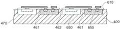
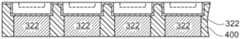
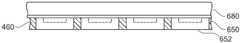
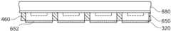
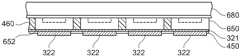
器件区可以与彼此横向地分离,并且可以按矩阵来被布置。例如,在器件区之间的碳化硅衬底的网格形部分可以形成切口区。也就是说,在往碳化硅衬底上的顶视图中,切口区可以具有网格的形状。切口区可没有变成半导体器件的组成部分的这样的元件和结构。切口区可以包括在晶圆级的制造过程和器件表征期间被临时使用的元件和结构,例如电气测试电路和/或对准标记。切口区的一部分可以在切块过程期间被消耗。例如,使用机械锯或激光的切块过程可以在器件区之间的切口区中产生划线。The device regions may be laterally separated from each other, and may be arranged in a matrix. For example, a grid-shaped portion of a silicon carbide substrate between device regions may form kerf regions. That is, in a top view onto a silicon carbide substrate, the cutout regions may have the shape of a grid. The cutout region may be free of such elements and structures that become an integral part of the semiconductor device. The kerf area may include components and structures that are temporarily used during wafer-level manufacturing processes and device characterization, such as electrical test circuits and/or alignment marks. A portion of the cutout area may be consumed during the dicing process. For example, a dicing process using a mechanical saw or laser can create scribe lines in the kerf regions between device regions.
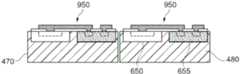
辅助载体在碳化硅衬底的前侧处与碳化硅衬底在结构上连接。辅助载体可以与主要表面直接接触,或者具有与碳化硅衬底和/或辅助载体的材料不同的材料的一个或多个层或结构可以被形成在辅助载体和主要表面之间。如果在辅助载体和主要表面之间形成了多个层或结构,则所述层或结构可按其材料而不同。所述层(或结构)中的至少一个可以与碳化硅衬底和辅助载体中的至少一个直接接触。例如,与器件区中的掺杂区电气接触的前侧金属化部和/或使前侧金属化部的近邻部分电气绝缘的绝缘结构可以被形成在辅助载体与碳化硅衬底的主要表面之间。The auxiliary carrier is structurally connected to the silicon carbide substrate at the front side of the silicon carbide substrate. The secondary carrier may be in direct contact with the primary surface, or one or more layers or structures of a different material than that of the silicon carbide substrate and/or secondary carrier may be formed between the secondary carrier and the primary surface. If multiple layers or structures are formed between the auxiliary support and the primary surface, the layers or structures may vary according to their materials. At least one of the layers (or structures) may be in direct contact with at least one of the silicon carbide substrate and the auxiliary carrier. For example, front-side metallization in electrical contact with doped regions in the device region and/or insulating structures that electrically insulate adjacent portions of the front-side metallization may be formed between the auxiliary carrier and the major surface of the silicon carbide substrate between.
在一些实施例中,辅助载体可以与碳化硅衬底、与碳化硅衬底的主要表面上的前侧金属化部和/或与所述主要表面上的绝缘结构可逆地连接。例如,辅助载体可以通过胶、粘合层和/或粘合箔而被可逆地结合到碳化硅衬底的前侧。在该上下文中,“可逆地”可以意指:可以在不毁坏碳化硅衬底和/或辅助载体的情况下从碳化硅衬底移除辅助载体,例如通过使用机械力、化学溶剂、热学能量和/或辐射能量(例如利用UV和/或激光辐射)。In some embodiments, the auxiliary carrier may be reversibly connected to the silicon carbide substrate, to the front-side metallization on a major surface of the silicon carbide substrate, and/or to insulating structures on the major surface. For example, the auxiliary carrier may be reversibly bonded to the front side of the silicon carbide substrate by glue, adhesive layer and/or adhesive foil. In this context, "reversibly" may mean that the auxiliary support can be removed from the silicon carbide substrate without destroying the silicon carbide substrate and/or the auxiliary support, eg by using mechanical force, chemical solvents, thermal energy and/or radiant energy (eg with UV and/or laser radiation).
在其它实施例中,辅助载体可以与碳化硅衬底不可逆地连接。例如,在结构上地连接辅助载体与碳化硅衬底可以包括以下中的至少一个:直接结合、反应性结合、摩擦结合、焊接(例如扩散焊接)。如果辅助载体由具有玻璃的源材料形成,则所述源材料作为示例可以包括玻璃粉和/或玻璃熔块。In other embodiments, the auxiliary carrier may be irreversibly connected to the silicon carbide substrate. For example, structurally connecting the auxiliary carrier to the silicon carbide substrate may include at least one of: direct bonding, reactive bonding, friction bonding, welding (eg, diffusion welding). If the auxiliary carrier is formed from a source material having glass, the source material may include, by way of example, glass frit and/or glass frit.
在直接结合的情况中,辅助载体的工作表面以及在碳化硅衬底的前侧处的顶表面足够平坦、光滑和洁净。在直接结合的辅助载体与碳化硅衬底的前侧处的顶表面之间的粘合可以基于在碳化硅衬底与辅助载体之间的化学键、氢键、范德瓦尔斯键、金属键、离子键和/或共价键。直接结合可以包括:施加物理力,所述物理力将碳化硅衬底和辅助载体对着彼此按压;在中等温度下对两个结合表面中至少一个的热处理;或者二者的组合(熔合结合、热压缩结合、通过原子重布置的结合)。直接结合可以包括不存在任何附加的中间层。In the case of direct bonding, the working surface of the auxiliary carrier and the top surface at the front side of the silicon carbide substrate are sufficiently flat, smooth and clean. The adhesion between the directly bonded auxiliary support and the top surface at the front side of the silicon carbide substrate may be based on chemical bonds, hydrogen bonds, van der Waals bonds, metallic bonds, Ionic and/or covalent bonds. Direct bonding may include: application of physical forces that press the silicon carbide substrate and auxiliary carrier against each other; thermal treatment of at least one of the two bonding surfaces at moderate temperatures; or a combination of the two (fusion bonding, thermocompression bonding, bonding by atomic rearrangement). Direct bonding may include the absence of any additional intervening layers.
直接结合和反应性结合可以在比较低的温度下被执行,使得可以提供辅助载体,而没有对碳化硅衬底中先前形成的结构的显著影响。Direct bonding and reactive bonding can be performed at relatively low temperatures, so that auxiliary supports can be provided without significant effects on previously formed structures in the silicon carbide substrate.
在辅助载体包括金属的情况下,将辅助载体在结构上连接在碳化硅衬底的前侧处可以包括焊接、扩散焊接、烧结和/或摩擦结合。扩散焊接可以包括将扩散焊接材料施加在辅助载体的工作表面上和/或在碳化硅衬底的前侧、例如前侧金属化部上。扩散焊料可以包括锡(Sn)和至少一种另外的金属。例如,扩散焊料可以无铅并且可以包括Sn以及Ni、In、Pd、Mo、Cu、Au和Ag中的至少一个。烧结可以包括将烧结膏(sinter paste)施加在辅助载体的工作表面与碳化硅衬底的前侧中的至少一个上,其中所述烧结膏可以包括银和铜中的至少一个。Where the auxiliary carrier comprises metal, structurally attaching the auxiliary carrier at the front side of the silicon carbide substrate may include welding, diffusion welding, sintering and/or friction bonding. Diffusion bonding may include applying diffusion bonding material on the working surface of the auxiliary carrier and/or on the front side, eg, front side metallization, of the silicon carbide substrate. The diffusion solder may include tin (Sn) and at least one other metal. For example, the diffusion solder may be lead-free and may include Sn and at least one of Ni, In, Pd, Mo, Cu, Au, and Ag. Sintering can include applying a sinter paste on at least one of the working surface of the auxiliary carrier and the front side of the silicon carbide substrate, wherein the sinter paste can include at least one of silver and copper.
辅助载体可以包括环形部分。辅助载体、特别是辅助载体的环形部分可以在没有粘合层的情况下被结合到碳化硅衬底(例如经由前侧金属化部)。也就是说,在碳化硅衬底与辅助载体和/或辅助载体的环形部分之间的结合可以无粘合层。例如,热学结合可以用于无粘合层的结合。The auxiliary carrier may comprise an annular portion. The auxiliary carrier, in particular the annular portion of the auxiliary carrier, can be bonded to the silicon carbide substrate (eg via the front side metallization) without an adhesive layer. That is, the bond between the silicon carbide substrate and the auxiliary carrier and/or the annular portion of the auxiliary carrier may be free of an adhesive layer. For example, thermal bonding can be used for bonding without an adhesive layer.
例如在晶圆级所应用的过程期间,辅助载体可以形成用于碳化硅衬底的机械稳定载体。在下文中,“机械稳定”意指在后续过程步骤中可以利用适当的工具来处置碳化硅衬底,而无需另外的衬底,例如用于防止碳化硅衬底的破裂或弯曲和/或用于易于处置。在至少一个方法步骤中,辅助载体可以是仅有的用于碳化硅衬底的机械稳定结构。例如,在晶圆薄化过程期间,辅助载体可以使碳化硅衬底稳定。The auxiliary carrier may form a mechanically stable carrier for silicon carbide substrates, for example during processes applied at the wafer level. In the following, "mechanically stable" means that the silicon carbide substrate can be handled with suitable tools in subsequent process steps without additional substrates, eg for preventing cracking or bending of the silicon carbide substrate and/or for Easy to handle. In at least one method step, the auxiliary carrier may be the only mechanically stable structure for the silicon carbide substrate. For example, the auxiliary carrier can stabilize the silicon carbide substrate during the wafer thinning process.
可以移除空闲层。移除空闲层包括晶圆薄化过程,例如从背侧研磨碳化硅衬底或将空闲层从器件层拆分。Idle layers can be removed. Removing the idler layer includes wafer thinning processes such as backside grinding of the silicon carbide substrate or splitting the idler layer from the device layer.
由于在晶圆薄化过程之后和/或直到管芯分离为止,辅助载体可以使碳化硅衬底机械地稳定,所以可减小碳化硅衬底的厚度。碳化硅衬底的厚度可以被减小到碳化硅衬底的直径的0.3%以下(或0.2%以下或0.15%以下)的厚度。例如,厚度可以被减小到180μm以下,例如到110μm以下,到90μm以下,或到至多70μm。最终厚度可取决于碳化硅衬底的直径。例如,如果碳化硅衬底具有6英寸的直径,则厚度可以被减小到110μm以下。The thickness of the silicon carbide substrate can be reduced because the auxiliary carrier can mechanically stabilize the silicon carbide substrate after the wafer thinning process and/or until the dies are separated. The thickness of the silicon carbide substrate may be reduced to a thickness of 0.3% or less (or 0.2% or less or 0.15% or less) of the diameter of the silicon carbide substrate. For example, the thickness may be reduced to below 180 μm, for example to below 110 μm, to below 90 μm, or to at most 70 μm. The final thickness may depend on the diameter of the silicon carbide substrate. For example, if the silicon carbide substrate has a diameter of 6 inches, the thickness can be reduced to below 110 μm.
形成模塑结构。模塑结构填充网格形的凹槽,所述网格形的凹槽横向地分离器件层中的器件区。可以在移除空闲层之前或在移除空闲层之后在切块过程中在切口区的一部分中形成网格形凹槽。A molded structure is formed. The molding structure fills the grid-shaped grooves that laterally separate device regions in the device layer. The grid-shaped grooves may be formed in a portion of the kerf region during the dicing process before removing the free layer or after removing the free layer.
可以由如下材料形成模塑结构:所述材料由玻璃(例如具有在500℃以下的玻璃转变温度的低熔点玻璃)、陶瓷材料、或基于聚合物的材料构成或包括所述各项。例如,模塑结构可以包括硅树脂(silicone)、聚酰亚胺、环氧树脂和/或聚四氟乙烯,其中用于晶圆级封装技术、诸如eWLB(嵌入式晶圆级球栅阵列)封装的过程和工具可以用于以成本有效的方式形成模塑结构。The molded structure may be formed from or including a glass (eg, a low melting point glass having a glass transition temperature below 500°C), a ceramic material, or a polymer-based material. For example, the molded structure may include silicone, polyimide, epoxy, and/or Teflon, which are used in wafer level packaging techniques such as eWLB (Embedded Wafer Level Ball Grid Array) The encapsulated process and tools can be used to form the molded structure in a cost-effective manner.
在具有平面表面的衬底中,网格形的凹槽可以包括第一平行条带凹槽的集合,以及以大于0度的角度、例如至少45度、至少80度和/或以90度、即正交地与第一条带凹槽相交的第二平行条带凹槽的集合。所述第一和第二条带凹槽可以具有相同的深度。在近邻的第一条带凹槽对与近邻的第二条带凹槽对之间的衬底部分可以形成从凹槽底平面突出的台面,其中台面的共平面的水平横截面可以具有相同的形状和面积。可替换地,网格形凹槽可以限定六边形的衬底部分。In a substrate having a planar surface, the grid-shaped grooves may comprise a collection of first parallel strip grooves, and at an angle greater than 0 degrees, for example at least 45 degrees, at least 80 degrees and/or at 90 degrees, That is, a set of second parallel strip grooves that intersect the first strip groove orthogonally. The first and second strip grooves may have the same depth. The portion of the substrate between the adjacent first pair of strip grooves and the adjacent second pair of strip grooves may form mesas protruding from the groove bottom plane, wherein the coplanar horizontal cross-sections of the mesas may have the same shape and area. Alternatively, the grid-shaped grooves may define hexagonal substrate portions.
在切块之后,每个器件区形成单个半导体管芯,其中辅助载体和半导体管芯形成晶圆复合物,其中半导体管芯处于其原始定位处。After dicing, each device region forms a single semiconductor die, wherein the auxiliary carrier and the semiconductor die form a wafer composite with the semiconductor die in its original position.
形成模塑结构可以包括注塑和/或使用两件式模塑物的模塑过程。碳化硅衬底的背侧可以充当第一模塑件。被安置在距碳化硅衬底的背侧的某个距离处的平坦模塑件可以充当第二模塑件。在碳化硅衬底与平坦模塑件之间的空间填充有液体模塑树脂,所述液体模塑树脂还填充网格形凹槽。在凝固和/或固化之后,模塑树脂形成刚性模塑结构。Forming the molded structure may include injection molding and/or a molding process using a two-piece molding. The backside of the silicon carbide substrate can serve as the first molding. A flat molding placed at a distance from the backside of the silicon carbide substrate can serve as the second molding. The space between the silicon carbide substrate and the flat molding is filled with a liquid molding resin, which also fills the grid-shaped grooves. After setting and/or curing, the molding resin forms a rigid molding structure.
模塑结构可以将已经被切块的器件区保持在器件区在切块之前所具有的相对于彼此的定位处。在模塑过程之后,器件区仍可以被直接固定到辅助载体。包括模塑结构和经切块的器件区的晶圆复合物允许在晶圆级的另外的处理,例如晶圆级封装过程、比如eWLB封装。The molding structure can maintain the device regions that have been diced in the orientations relative to each other that the device regions had prior to dicing. After the molding process, the device area can still be directly fixed to the auxiliary carrier. Wafer composites including molded structures and diced device regions allow for additional processing at the wafer level, such as wafer level packaging processes, such as eWLB packaging.
模塑结构可以仅包括网格形凹槽中的模塑树脂的部分。模塑结构可以形成刚性辅助网格,其横向地嵌入每一个器件区。辅助网格可以促进在晶圆级的另外过程、例如器件表征的应用。器件表征(例如管芯分类和/或电气分类)可以包括针对每个半导体管芯的电气测试。The molded structure may include only the portion of the molding resin in the grid-shaped grooves. The molded structure may form a rigid auxiliary grid that is embedded laterally in each device region. Auxiliary grids can facilitate the application of additional processes at the wafer level, such as device characterization. Device characterization (eg, die classification and/or electrical classification) may include electrical testing for each semiconductor die.
然后,器件区可以与彼此分离,其中模塑结构的部分形成框架结构,所述框架结构横向地围绕器件区。分离可以涉及分离和/或移除模塑结构的部分。形成框架结构的模塑结构的部分可以是模塑结构的剩余部分和/或残余物。已经被切块的器件区(即半导体管芯)与彼此的分离可以包括标准化的锯切过程,其仅仅切穿模塑结构。所述方法避免锯(或类似的机械、研磨工具)与半导体管芯的侧壁的机械接触。沿着半导体管芯的侧壁对半导体材料的切削可以被有效地避免,并且过程产出增大。The device regions can then be separated from each other, wherein portions of the molded structure form a frame structure that laterally surrounds the device regions. Separation may involve separating and/or removing portions of the molded structure. The portion of the molded structure that forms the frame structure may be the remainder and/or residue of the molded structure. Separation of the device regions (ie, semiconductor dies) that have been diced from each other may include a standardized sawing process that only cuts through the molded structure. The method avoids mechanical contact of the saw (or similar mechanical, abrasive tool) with the sidewalls of the semiconductor die. Cutting of semiconductor material along the sidewalls of the semiconductor die can be effectively avoided, and process yield is increased.
得自模塑材料的框架结构可以形成与半导体管芯的侧壁直接接触的形状配合的壳体,并且可以有效地保护半导体管芯免受潮湿、污染和电荷。另外,框架结构可以增大器件可靠性。The frame structure derived from the molding material can form a form-fit housing that is in direct contact with the sidewalls of the semiconductor die and can effectively protect the semiconductor die from moisture, contamination and electrical charges. In addition, the frame structure can increase device reliability.
根据实施例,可以在移除空闲层之前形成凹槽。可以在器件区中形成功能性电路之后或其期间形成凹槽。例如,可以在碳化硅衬底的主要表面上形成前侧金属化部之前或之后形成凹槽。典型地,在使前侧金属化部结构化之后形成凹槽。凹槽可以减小半导体衬底的机械应力和/或弯曲。碳化硅衬底中的凹槽的深度可以等于或大于半导体管芯的最终垂直延伸。According to an embodiment, the grooves may be formed before removing the idle layer. The recesses may be formed after or during the formation of functional circuits in the device region. For example, the grooves may be formed before or after the front side metallization is formed on the major surface of the silicon carbide substrate. Typically, the grooves are formed after structuring the front side metallization. The grooves can reduce mechanical stress and/or bending of the semiconductor substrate. The depth of the grooves in the silicon carbide substrate may be equal to or greater than the final vertical extension of the semiconductor die.
凹槽可以至少部分地填充有一层或层系统,其包括能够在对照碳化硅衬底的材料的高选择性的情况下被移除的至少一种材料,例如环氧树脂、BCB(苯并环丁烯、C8H8)、PNB(聚降冰片烯)、SOS(旋涂硅)、SOG(旋涂玻璃)、或经掺杂或未经掺杂的玻璃。The grooves may be at least partially filled with a layer or layer system comprising at least one material that can be removed with high selectivity compared to the material of the silicon carbide substrate, such as epoxy, BCB (benzoic ring) Butene,C8H8 ), PNB (polynorbornene), SOS (spinon silicon), SOG (spin on glass), or doped or undoped glass.
根据另一实施例,可以在移除空闲层之后形成凹槽。以此方式,有可能的是,器件层在空闲层的移除期间示出高机械稳定性。According to another embodiment, the grooves may be formed after removing the idler layer. In this way, it is possible that the device layer shows high mechanical stability during removal of the idle layer.
根据实施例,在模塑之前可以重装配和/或重分布器件区,使得碳化硅衬底的器件区中的至少一个被从另外的半导体衬底所获得的补充器件区所取代。例如,所述另外的器件区可以包括具有与在碳化硅衬底的器件区中所形成的电子元件不同的电气功能的电子元件。According to an embodiment, the device regions may be reassembled and/or redistributed prior to molding such that at least one of the device regions of the silicon carbide substrate is replaced by complementary device regions obtained from another semiconductor substrate. For example, the additional device regions may include electronic components having different electrical functions than electronic components formed in the device regions of the silicon carbide substrate.
可以在模塑结构中和/或其上形成导线。导线可以电气地连接来自碳化硅衬底的器件区的导电结构以及来自所述另外的半导体衬底的器件区的导电结构。例如,具有不同功能性和/或得自不同半导体材料的半导体管芯可以被组合在单一的模塑结构中。终定的混合半导体器件包括从至少两个不同的半导体衬底所获得的半导体管芯,其中模塑结构的分离部分将所述至少两个半导体管芯与彼此横向地分离,并且框架结构形成在混合半导体器件的所有半导体管芯周围的公共框架。因此,器件区中的多于一个可以用补充器件区取代,其中可以使用不同类型的补充半导体管芯。Wires may be formed in and/or on the molded structure. The wires may electrically connect the conductive structures from the device region of the silicon carbide substrate and the conductive structures from the device region of the further semiconductor substrate. For example, semiconductor dies having different functionality and/or derived from different semiconductor materials may be combined in a single molded structure. The final hybrid semiconductor device includes semiconductor dies obtained from at least two different semiconductor substrates, wherein a separating portion of the molding structure laterally separates the at least two semiconductor dies from each other, and the frame structure is formed in the A common frame around all semiconductor dies of a hybrid semiconductor device. Accordingly, more than one of the device regions may be replaced with complementary device regions, wherein different types of complementary semiconductor dies may be used.
根据实施例,在形成模塑结构之后并且在分离器件区之前,可以在器件区的背侧表面上选择性地形成背侧金属结构。在模塑结构上不形成背侧金属结构(即,模塑结构可以无背侧金属结构)。代替地,模塑结构可以支持背侧金属结构的至少一部分的自对准的形成,或者可以为图案电镀过程提供平坦表面,其形成背侧金属结构的至少一部分。According to an embodiment, a backside metal structure may be selectively formed on the backside surface of the device region after the molding structure is formed and before the device region is separated. No backside metal structure is formed on the molded structure (ie, the molded structure may be free of backside metal structure). Alternatively, the molded structure may support the self-aligned formation of at least a portion of the backside metal structure, or may provide a flat surface for a patterned electroplating process that forms at least a portion of the backside metal structure.
根据实施例,可以提供预制件用于形成模塑结构。可以在模塑之前或在模塑期间、作为模塑铸件(molding cast)的部分而提供所述预制件。所述预制件可以包括在器件区的背侧表面上的横向分离的模版部分,其中每个模版部分被指派到一个器件区。所述预制件可以此外包括框架部分,所述框架部分形成横向地围绕模版部分的闭合框架。当形成模塑结构的时候,模塑结构填充在模版部分之间以及在模版部分与框架部分之间的空间。According to an embodiment, a preform may be provided for forming the molded structure. The preform may be provided as part of a molding cast before or during molding. The preform may include laterally separated stencil portions on the backside surface of the device regions, wherein each stencil portion is assigned to a device region. The preform may further comprise a frame portion forming a closed frame laterally surrounding the stencil portion. When the molded structure is formed, the molded structure fills the space between the stencil portions and between the stencil portion and the frame portion.
以此方式,有可能的是:直接在具有网格形凹槽的切口区下方排他地形成模塑结构。直接在器件区下方没有模塑结构。所述预制件可以促进厚的背侧金属化部的至少一部分的自对准的形成。In this way, it is possible to exclusively form the moulding structure directly below the cutout area with the grid-shaped grooves. There is no molding structure directly below the device area. The preform may facilitate the self-aligned formation of at least a portion of the thick backside metallization.
根据实施例,可以在形成了模塑结构之后移除所述预制件。移除预制件的模版部分选择性地暴露器件区的背侧表面,并且促进厚的背侧金属化部的至少一部分的自对准的形成。According to an embodiment, the preform may be removed after the molded structure is formed. Removing the stencil portion of the preform selectively exposes the backside surface of the device region and facilitates the self-aligned formation of at least a portion of the thick backside metallization.
根据实施例,在移除了预制件的模版部分之后留下的空间中形成背侧金属结构的至少一部分。According to an embodiment, at least a portion of the backside metal structure is formed in the space left after removal of the stencil portion of the preform.
例如,可以施加金属膏,并且刮刀可以从模版部分的表面移除过量金属膏。烘烤过程可以使金属膏干燥,以由金属膏形成固体并且紧致的背侧金属结构。For example, a metal paste can be applied and a doctor blade can remove excess metal paste from the surface of the stencil portion. The baking process can dry the metal paste to form a solid and compact backside metal structure from the metal paste.
根据实施例,在应用预制件之前可以在经切块的器件层上形成金属种子层。金属种子层覆盖器件区的背侧表面和侧壁。在形成主要金属部分之前,可以移除辅助载体,其中金属种子层变得在晶圆复合物的前侧处可达,所述晶圆复合物包括模塑结构以及经切块的器件区。在晶圆复合物的背侧上,通过移除预制件的模版部分所留下的空间暴露在器件区的背侧表面上所形成的金属种子层的区段。电化学沉积过程可以形成背侧金属结构的厚的主要金属部分,其选择性地生长在器件区的背侧上的金属种子层的所暴露的部分中的多部分上。According to an embodiment, a metal seed layer may be formed on the diced device layer prior to applying the preform. The metal seed layer covers the backside surface and sidewalls of the device region. Before forming the main metal portion, the secondary carrier may be removed, wherein the metal seed layer becomes accessible at the front side of the wafer composite including the molded structure and diced device regions. On the backside of the wafer composite, segments of the metal seed layer formed on the backside surface of the device region are exposed by removing the space left by the stencil portion of the preform. The electrochemical deposition process can form a thick main metal portion of the backside metal structure that is selectively grown on many of the exposed portions of the metal seed layer on the backside of the device region.
根据实施例,金属种子层可以包括在面向器件区的辅助载体的侧面上所形成的接入部分(access portion)。接入部分可以从最外面的器件区向外延伸。例如,接入部分可以沿着辅助载体的外周界形成环、环片段或多个环片段。According to an embodiment, the metal seed layer may include an access portion formed on a side of the auxiliary carrier facing the device region. The access portion may extend outward from the outermost device area. For example, the access moiety may form a loop, loop segment, or multiple loop segments along the outer perimeter of the helper carrier.
模塑结构可以被形成使得接入部分保持暴露并且对于在主要金属部分的电化学沉积期间所施加的电势而言可达。以此方式,有可能的是,辅助载体还在主要金属部分的电化学沉积期间使晶圆复合物机械稳定。可以在形成了主要金属部分之后移除辅助载体。The molded structure can be formed such that the access portion remains exposed and accessible to the potential applied during the electrochemical deposition of the primary metal portion. In this way, it is possible that the auxiliary carrier also mechanically stabilizes the wafer composite during the electrochemical deposition of the main metal part. The auxiliary carrier can be removed after the main metal portion is formed.
根据实施例,可以被形成在网格形凹槽外面的模塑结构的层部分被移除,使得横向分离的器件区的背侧表面被暴露。器件区和凹槽中的模塑结构形成平坦的后侧表面。According to an embodiment, the layer portion of the molding structure that may be formed outside the grid-shaped grooves is removed such that the backside surfaces of the laterally separated device regions are exposed. The device regions and the molded structures in the recesses form a flat backside surface.
根据实施例,在移除了模塑结构的层部分之后,可以在器件区的背侧表面上形成金属种子层。可以在金属种子层上形成背侧金属结构的横向分离的主要金属部分。形成主要金属部分可以包括图案电镀,其中以自对准的方式形成主要金属部分。According to an embodiment, a metal seed layer may be formed on the backside surface of the device region after removing the layer portion of the molding structure. The laterally separated main metal portions of the backside metal structure may be formed on the metal seed layer. Forming the main metal portion may include pattern electroplating, wherein the main metal portion is formed in a self-aligned manner.
根据实施例,在结构上连接辅助载体和碳化硅衬底之前,可以在碳化硅衬底的主要表面上形成前侧金属化部。以此方式,有可能的是:形成前侧金属化部是器件区的前侧处理的部分。According to an embodiment, a front side metallization may be formed on a major surface of the silicon carbide substrate prior to structurally connecting the auxiliary carrier and the silicon carbide substrate. In this way, it is possible that forming the front side metallization is part of the front side processing of the device region.
例如,有可能的是:直到器件分离的另外的过程仅仅应用在500摄氏度以下的温度,使得甚至在提供辅助载体之前所形成的前侧金属化部也可以包括铝(Al)。For example, it is possible that the further process until device separation is only applied at temperatures below 500 degrees Celsius, so that the front-side metallization formed even before the auxiliary carrier is provided may comprise aluminium (Al).
前侧金属化部可以用单件来被形成,或可以包括多个分离的部分。可以用多区段和/或多件的方式来形成分离的部分。此处并且在下文中,元件或所述元件的部分以“多区段的方式”被形成可以意指:元件的部分经由桥而被连接,所述桥可以小于所述部分。“多区段”元件的顶面可以是连贯的,但是不是简单地连贯。例如,“多区段”元件可以在所述元件的部分之间包括孔洞和/或间隙。此外,此处并且在下文中,元件或所述元件的部分以“多件方式”被形成可以意指:所述部分无互连,即所述部分与彼此分离。“多区段”元件的顶面可以不是连贯的。如果元件的部分同时“多区段”并且“多件”地被形成,则所述元件可以包括:第一零件,其中具有以多区段方式所形成的第一部分;以及第二零件,其中具有以多件方式所形成的第二部分,其中所述第一零件和第二零件关于彼此可以用多件方式来被形成。前侧金属化部的每个零件可以用一对一方式来被指派给器件区。The front side metallization may be formed in a single piece, or may comprise multiple separate parts. The separate parts may be formed in multiple sections and/or pieces. Here and in the following, an element or parts of said elements are formed in a "multi-section manner" may mean that parts of elements are connected via bridges, which bridges may be smaller than said parts. The top surface of a "multi-segment" element may be continuous, but is not simply continuous. For example, a "multi-section" element may include holes and/or gaps between portions of the element. Furthermore, here and below, an element or a portion of an element being formed in "multi-piece" may mean that the portions are not interconnected, ie, the portions are separated from each other. The top surface of a "multi-segment" element may not be continuous. If parts of an element are formed "multi-section" and "multi-piece" simultaneously, the element may comprise: a first part having the first part formed in a multi-section; and a second part, There is a second portion formed in multiple pieces, wherein the first and second pieces may be formed in multiple pieces with respect to each other. Each part of the front side metallization can be assigned to a device region in a one-to-one manner.
在早期阶段提供前侧金属化部还可以促进器件表征,其中在移除了辅助载体之后,半导体管芯是晶圆复合物的构件。Providing front-side metallization at an early stage can also facilitate device characterization, where the semiconductor die is a component of the wafer composite after the auxiliary carrier has been removed.
根据另一实施例,在分离辅助载体和碳化硅衬底之后,可以在碳化硅衬底的主要表面上形成前侧金属化部。以此方式,可以有可能的是,与在晶圆薄化期间和/或其之后所应用的温度预算独立地形成前侧金属化部。在其它实施例中,可以在分离辅助载体与碳化硅衬底之前和/或在晶圆薄化之前和/或在背侧金属结构的形成之前形成前侧金属化部。例如,前侧金属化部可以包括铝或铜,并且直到移除辅助载体为止被应用到晶圆复合物的过程不被限制到500℃的最大温度。According to another embodiment, after separating the auxiliary carrier and the silicon carbide substrate, the front side metallization may be formed on the main surface of the silicon carbide substrate. In this way, it may be possible to form the front side metallization independently of the temperature budget applied during and/or after wafer thinning. In other embodiments, the front side metallization may be formed prior to separation of the auxiliary carrier from the silicon carbide substrate and/or prior to wafer thinning and/or prior to formation of the back side metal structure. For example, the front side metallization may comprise aluminum or copper, and the process applied to the wafer composite is not limited to a maximum temperature of 500°C until the auxiliary carrier is removed.
根据实施例,移除空闲层包括将空闲层从器件层拆分。贯穿本申请,将碳化硅衬底的层部分拆分(例如将空闲层从器件层拆分)还可以被称为“拆分(split-off)方法”。经拆分的空闲层可以被重用于制造另外的半导体器件。因而,可以从单一的标准碳化硅晶圆获得多个薄的碳化硅衬底。According to an embodiment, removing the free layer includes splitting the free layer from the device layer. Throughout this application, splitting a layer portion of a silicon carbide substrate (eg, splitting an idle layer from a device layer) may also be referred to as a "split-off method." The split free layers can be reused to fabricate additional semiconductor devices. Thus, multiple thin silicon carbide substrates can be obtained from a single standard silicon carbide wafer.
可以沿着拆分区将空闲层从器件层拆分。拆分区可以是碳化硅衬底中的一层,其按至少一个物理性质和/或材料性质而不同于碳化硅衬底的其余部分。“碳化硅衬底的其余部分”可以是无拆分区并且围绕拆分区的碳化硅衬底的部分。例如,与碳化硅衬底的其余部分相比,拆分区可以具有不同的吸收系数(例如较高的吸收系数)、不同的带隙(例如较低的带隙)、不同的孔隙率(例如较高的孔隙率)、不同的机械稳定性、不同的材料组成、和/或不同的晶体结构(例如不同的多型体和/或不同的结晶度)。例如,拆分区可以包括已被注入到碳化硅衬底和/或多孔的碳化硅中的离子。拆分区可以具有与碳化硅衬底的厚度相比很小的厚度。拆分区的横向伸展可以是碳化硅衬底的横向伸展的至少90%或至少95%。换言之,拆分区可以大体上沿着整个碳化硅衬底横向地延伸。The free layer can be split from the device layer along the split zone. The split region may be a layer in the silicon carbide substrate that differs from the rest of the silicon carbide substrate by at least one physical property and/or material property. The "rest of the silicon carbide substrate" may be the portion of the silicon carbide substrate that is free of the split region and surrounds the split region. For example, the split region may have a different absorption coefficient (eg higher absorption coefficient), different band gap (eg lower band gap), different porosity (eg lower band gap) than the rest of the silicon carbide substrate higher porosity), different mechanical stability, different material compositions, and/or different crystal structures (eg, different polytypes and/or different degrees of crystallinity). For example, the split region may include ions that have been implanted into the silicon carbide substrate and/or the porous silicon carbide. The split region may have a thickness that is small compared to the thickness of the silicon carbide substrate. The lateral extension of the split region may be at least 90% or at least 95% of the lateral extension of the silicon carbide substrate. In other words, the split region may extend laterally along substantially the entire silicon carbide substrate.
拆分方法可以是激光辅助的拆分方法。也就是说,拆分方法可以涉及向碳化硅衬底应用激光辐射(即,利用激光辐射来辐照碳化硅衬底)。激光辐射可以在碳化硅衬底中创建拆分区,和/或可以被应用到碳化硅衬底中的拆分区。The splitting method may be a laser-assisted splitting method. That is, the splitting method may involve applying laser radiation to the silicon carbide substrate (ie, irradiating the silicon carbide substrate with laser radiation). Laser radiation can create split regions in a silicon carbide substrate, and/or can be applied to split regions in a silicon carbide substrate.
如果激光辐射将被应用到拆分区,则拆分区与碳化硅衬底的其余部分相比可以具有针对激光辐射波长的更高吸收系数。例如,拆分区中的吸收系数是碳化硅衬底的其余部分中的吸收系数的至少5倍、或至少20倍或至少100倍。If laser radiation is to be applied to the splitting region, the splitting region may have a higher absorption coefficient for the wavelength of the laser radiation than the rest of the silicon carbide substrate. For example, the absorption coefficient in the split region is at least 5 times, or at least 20 times, or at least 100 times the absorption coefficient in the rest of the silicon carbide substrate.
可以通过将离子注入到碳化硅衬底中来提供具有较高吸收系数的拆分区。离子可直接导致较高的吸收,其例如由于在离子下的较高吸收率所致,和/或可导致碳化硅衬底的晶体结构往不同的多型体(例如从4H-SiC向3C-SiC)和/或往不同的结晶度中的转换,使得针对激光辐射的吸收系数在拆分区中增大。通过将激光辐射应用到拆分区,可以沿着拆分区产生热机械应力,其可以促进和/或简化空闲层的移除。Splitting regions with higher absorption coefficients can be provided by implanting ions into silicon carbide substrates. The ions can directly lead to higher absorption, for example due to higher absorption rates under the ions, and/or can cause the crystal structure of the silicon carbide substrate to shift to a different polytype (eg from 4H-SiC to 3C- SiC) and/or conversion to a different crystallinity, so that the absorption coefficient for laser radiation increases in the split region. By applying laser radiation to the splitting zone, thermomechanical stresses can be created along the splitting zone, which can facilitate and/or simplify the removal of the free layer.
将被应用到拆分区的激光辐射可以处于共振状态,其中单光子过程(例如单光子吸收)占主导,即多光子过程的概率很小(例如是单光子过程的概率的至多十分之一)。在共振状态中,拆分区的带隙可以例如是激光辐射的光子能量的至多十倍(典型地至多两倍)。激光辐射可以在拆分区中被吸收,并且可导致对拆分区的损坏,使得对于拆分碳化硅衬底而言不需要任何机械力和/或热应力或仅仅需要小的机械力和/或热应力。在共振状态中,激光辅助的拆分方法还可以被称为激光剥离。The laser radiation to be applied to the splitting region can be in a resonance state in which single-photon processes (eg single-photon absorption) dominate, i.e. the probability of multi-photon processes is small (eg at most one tenth of the probability of single-photon processes) ). In the resonant state, the band gap of the splitting region may be, for example, up to ten times (typically up to twice) the photon energy of the laser radiation. The laser radiation can be absorbed in the cleavage zone and can cause damage to the cleavage zone, so that no mechanical and/or thermal stress or only small mechanical forces and/or only small mechanical forces and/or are required for cleaving the silicon carbide substrate or thermal stress. In the resonance state, the laser-assisted dissociation method can also be referred to as laser lift-off.
如果拆分区通过激光辐射来被创建,则可以通过向碳化硅衬底内的经很好地限定的区(例如具有拆分区的厚度的区)聚焦激光辐射来限定拆分区。在该情况中,激光辐射可以处于非共振状态,使得拆分区中的单光子过程的概率基本上是零,并且仅有多光子过程(例如多光子吸收)可能必须被考虑。例如,如果拆分区的带隙是激光辐射的光子能量的至少两倍(典型地至少十倍),则可以实现非共振状态。应用处于非共振状态的激光辐射,例如通过将激光辐射聚焦到经很好地限定的区,可导致产生穿孔平面(其可对应于拆分区)。在该情况中,激光辅助的拆分方法还可以被称为激光调节。在穿孔平面内,相比于碳化硅衬底的其余部分,热-机械应力可增大,因而简化对碳化硅衬底的拆分,例如通过向碳化硅衬底施加机械力和/或热应力。If the split region is created by laser radiation, the split region can be defined by focusing the laser radiation on a well-defined region (eg, a region having the thickness of the split region) within the silicon carbide substrate. In this case, the laser radiation may be in a non-resonant state such that the probability of single-photon processes in the split region is substantially zero, and only multi-photon processes (eg multi-photon absorption) may have to be considered. For example, an off-resonance state can be achieved if the band gap of the splitting region is at least twice (typically at least ten times) the photon energy of the laser radiation. Application of laser radiation in an off-resonance state, eg by focusing the laser radiation to a well-defined region, can result in the creation of perforated planes (which may correspond to split regions). In this case, the laser-assisted splitting method may also be referred to as laser conditioning. In the through-hole plane, thermal-mechanical stress can be increased compared to the rest of the silicon carbide substrate, thus simplifying disassembly of the silicon carbide substrate, eg by applying mechanical and/or thermal stress to the silicon carbide substrate .
根据实施例,可以提供碳化硅衬底,其包括多个器件区以及横向地分离器件区的网格形切口区。可以在切口区的背侧表面上形成模塑结构。在器件区的背侧表面上形成背侧金属结构。器件区被分离,其中模塑结构的部分形成框架结构,所述框架结构横向地围绕背侧金属结构。According to an embodiment, a silicon carbide substrate may be provided that includes a plurality of device regions and grid-shaped cutout regions that laterally separate the device regions. A molded structure may be formed on the backside surface of the cutout area. A backside metal structure is formed on the backside surface of the device region. The device regions are separated, wherein portions of the molded structure form a frame structure that laterally surrounds the backside metal structure.
根据另一实施例,半导体器件可以包括碳化硅主体、在碳化硅主体的前侧处的第一负载电极以及在碳化硅主体的背侧处的第二负载电极。可以包括基于聚合物的材料的框架结构与碳化硅主体的侧壁接触,并且横向地完全围绕至少碳化硅主体。框架结构可以沿着碳化硅主体的完整的垂直延伸而覆盖碳化硅主体的侧壁。在第一负载电极上方可没有框架结构。According to another embodiment, a semiconductor device may include a silicon carbide body, a first load electrode at a front side of the silicon carbide body, and a second load electrode at a back side of the silicon carbide body. The frame structure, which may include a polymer-based material, is in contact with the sidewalls of the silicon carbide body and laterally completely surrounds at least the silicon carbide body. The frame structure may cover the sidewalls of the silicon carbide body along the complete vertical extension of the silicon carbide body. There may be no frame structure above the first load electrode.
所述基于聚合物的材料可以由以下各项中至少一个构成或包括以下各项中至少一个:硅树脂、环氧树脂、聚酰亚胺和聚四氟乙烯。根据另一实施例,框架结构可以包括陶瓷材料或玻璃,例如具有在500℃以下的玻璃转变温度的低熔点玻璃。The polymer-based material may consist of or include at least one of the following: silicone, epoxy, polyimide, and polytetrafluoroethylene. According to another embodiment, the frame structure may comprise a ceramic material or glass, such as a low melting glass having a glass transition temperature below 500°C.
通常,基于聚合物的材料可以被用作用于框架结构的材料。可以根据以下性质中的至少一个来选择框架结构的材料:密度、长期稳定性、机械强度。用于晶圆级封装技术、诸如eWLB的过程和工具可以用于以成本有效的方式形成框架结构。Generally, polymer-based materials can be used as materials for frame structures. The material of the frame structure may be selected according to at least one of the following properties: density, long-term stability, mechanical strength. Processes and tools for wafer level packaging techniques, such as eWLB, can be used to form frame structures in a cost-effective manner.
框架结构可以提供闭合的、形状配合的套筒,其有效地保护碳化硅主体免受潮湿和污染,例如在带电离子、电子情况下的污染,和/或免受在不带电粒子情况下的污染。另外,框架结构可以促进半导体器件自晶圆复合物的简单、可靠并且成本有效的分离。The frame structure can provide a closed, form-fit sleeve that effectively protects the silicon carbide body from moisture and contamination, such as contamination in the case of charged ions, electrons, and/or contamination in the case of uncharged particles . Additionally, the frame structure can facilitate simple, reliable and cost-effective separation of semiconductor devices from the wafer composite.
根据其它实施例,半导体器件可以包括得自另一半导体材料、例如硅、锗或者另一宽带隙材料、诸如氮化镓(GaN)、氮化铝(AlN)或氧化镓(Ga2O3)的半导体主体。According to other embodiments, the semiconductor device may comprise derived from another semiconductor material such as silicon, germanium or another wide band gap material such as gallium nitride (GaN), aluminum nitride (AlN) or gallium oxide (Ga2O3) . the semiconductor body.
根据实施例,碳化硅主体可以包括第一掺杂区和第二掺杂区,其中所述第一掺杂区和第二掺杂区可以形成pn结和/或可以直接与彼此邻接。第一负载电极可以与第一掺杂区接触。第二负载电极可以与第二掺杂区接触。框架结构可以有效地保护垂直功率半导体器件的碳化硅主体免受污染和潮湿。According to an embodiment, the silicon carbide body may comprise a first doped region and a second doped region, wherein the first doped region and the second doped region may form a pn junction and/or may directly adjoin each other. The first load electrode may be in contact with the first doped region. The second load electrode may be in contact with the second doped region. The frame structure can effectively protect the silicon carbide body of the vertical power semiconductor device from contamination and moisture.
根据实施例,形成框架结构的材料可以包括以下各项中至少一个:环氧树脂、聚酰亚胺、聚四氟乙烯、硅树脂。用于晶圆级封装技术、诸如eWLB的过程和工具可以用于以成本有效的方式形成框架结构。According to an embodiment, the material forming the frame structure may include at least one of the following: epoxy, polyimide, polytetrafluoroethylene, silicone. Processes and tools for wafer level packaging techniques, such as eWLB, can be used to form frame structures in a cost-effective manner.
根据实施例,框架结构可以横向地围绕第二负载电极。框架结构可以形成一件式、形状配合的套筒,其包裹在碳化硅主体和第二负载电极二者周围。框架结构因而还可以有效地保护在碳化硅主体与第二负载电极之间的边缘免受潮湿和污染。According to an embodiment, the frame structure may laterally surround the second load electrode. The frame structure may form a one-piece, form-fitting sleeve that wraps around both the silicon carbide body and the second load electrode. The frame structure can thus also effectively protect the edge between the silicon carbide body and the second load electrode from moisture and contamination.
根据实施例,半导体器件可以此外包括端子、电气地连接所述端子和第一负载电极的接合线/金属夹片、以及包封所述接合线/金属夹片的模塑主体。模塑主体和框架结构的材料是不同的。来自晶圆级封装技术、诸如eWLB的领域的方法和材料可以与IC封装技术相组合以改善总体器件可靠性。According to an embodiment, the semiconductor device may further include a terminal, a bond wire/metal clip electrically connecting the terminal and the first load electrode, and a molded body encapsulating the bond wire/metal clip. The materials of the molded body and the frame structure are different. Methods and materials from the field of wafer level packaging technology, such as eWLB, can be combined with IC packaging technology to improve overall device reliability.
图1A-1D图示了一种方法,其包括在横向地分离器件层的器件区的网格形凹槽中形成模塑结构。1A-1D illustrate a method that includes forming a molding structure in a grid of grooves that laterally separate device regions of a device layer.
图1A示出了晶圆组装件900,其包括碳化硅衬底700以及辅助载体680。其它实施例可以涉及晶圆组装件900,其中碳化硅衬底700被另一半导体衬底取代,所述另一半导体衬底可以基于另一宽带隙半导体材料、诸如氮化镓(GaN)、氮化铝(AlN)或氧化镓(Ga2O3)。FIG. 1A shows a
碳化硅衬底700可以是平坦的板,其具有对应于标准晶圆尺寸的直径的直径,例如2英寸(51mm)、3英寸(76mm)、4英寸(100mm)、125mm或200mm。碳化硅衬底700的横截面可以是椭圆(尤其是圆形)的或多边形(尤其是六边形)的。碳化硅衬底700可以基于碳化硅晶体,其包括作为主要成分的硅和碳。碳化硅晶体可以包括另外的材料,例如作为材料和过程不完美和/或有意的添加剂的结果的非有意的杂质。非有意的杂质可以包括氧。有意的添加剂可以包括氢和/或掺杂剂原子,例如氮(N)、磷(P)、铍(Be)、硼(B)、铝(Al)和/或镓(Ga)。在碳化硅衬底700的前侧处的主要表面701上的表面法线704限定垂直方向。与表面法线704正交的方向是横向方向(有时也被称为“水平方向”)。
在碳化硅衬底700的主要表面701与背侧表面702之间的碳化硅衬底700的厚度可以等于或小于针对相同直径的标准碳化硅晶圆的厚度。例如,厚度可以小于180μm、小于110μm、小于90μm或至多70μm。The thickness of
碳化硅衬底700可以包括器件层750和空闲层760。器件层750与主要表面701邻接。在器件层750与背侧表面702之间形成空闲层760。
器件层750包括多个横向分离的器件区650。换言之,器件区650被横向地间隔,例如通过凹槽、另一材料的结构、或器件层750的另一部分。
每个器件区650可以包括多个掺杂区。例如,每个器件区650可以至少包括第一掺杂区120、例如发射极区,以及第二掺杂区130、例如漂移结构。第一掺杂区120和第二掺杂区130可以形成pn结pn。第一掺杂区120可以包括功率半导体二极管的阳极区,或可以包括IGFET、MCD或IGBT的主体区。凹槽770可以将器件区650与彼此横向地分离。在水平横截面中,凹槽770是网格形的。凹槽770从主要表面701延伸到器件层750中,并且可以抵达空闲层760或可以延伸到空闲层760中。Each
凹槽770可以完全填充有气体,例如填充有环境空气,或可以填充有固体牺牲材料,所述固体牺牲材料可以在对照器件区650的材料的高选择性的情况下被容易地移除。例如,凹槽770可以部分地或完全地填充有无机或有机材料。例如,可以使用以下材料中的至少一个:树脂、玻璃、聚酰亚胺、非晶硅、多晶硅、氧化硅、或其任何组合。Recess 770 can be completely filled with gas, eg, ambient air, or can be filled with solid sacrificial material that can be easily removed with high selectivity compared to the material of
在碳化硅衬底700的前侧处提供辅助载体680。辅助载体680可以与主要表面701直接接触。可替换地,可以在辅助载体608与主要表面701之间形成前侧金属化部、层间电介质和/或钝化结构,其中可以在前侧金属化部的部分与碳化硅衬底700的部分之间形成层间电介质,并且其中钝化结构可以覆盖前侧金属化部和/或层间电介质的边缘部分。
辅助载体680可以具有均匀厚度的板的形状,或环的形状,其沿着碳化硅衬底700的周界而延伸。可替换地,辅助载体680可以是板,其具有在器件区650上方的多个开口。The
例如,辅助载体680可以是或可以包括金属板。可替换地,辅助载体680可以通过压模来被形成,其中对着碳化硅衬底700所按压的源材料暂时被加热到源材料的玻璃转变温度以上。辅助载体680可以形成有开口,所述开口暴露器件区650上的前侧金属化部的区段。For example, the
辅助载体680可以包括主要载体682、例如半导体板、绝缘体板或金属板,其通过粘合层681而被附连到碳化硅衬底700的前侧。粘合层681将主要载体682粘合性结合到碳化硅衬底700上或前侧金属化部上。粘合层681可以由暂时的结合/解除结合粘合剂形成。例如,液体胶(即液体粘合剂)可以被施加到碳化硅衬底700的前侧上。预烘烤可以使胶干燥和/或固化,和/或移除溶剂。分离地或相组合地,可以通过利用向粘合剂的电磁辐射(例如UV辐射)来照射胶而使液体粘合剂干燥和/或固化和/或变换。固化还可以通过等待足够量的时间来被实现。可以使主要载体682与胶的经暴露的顶表面接触。然后,胶可以固化或进一步固化以形成如上所述的粘合层681。
可替换地,粘合层681可以是或可以包括粘合带,其粘合性结合主要载体682与半导体衬底700。粘合层681在主要载体682与碳化硅衬底700之间形成可逆连接,使得在从碳化硅衬底700分离了辅助载体680之后,辅助载体680可以被重用。Alternatively,
可替换地,辅助载体680和半导体衬底700可以被不可逆地结合到彼此,以减小碳化硅衬底700的弯曲。不可逆地结合的辅助载体680的移除可以包括研磨或抛光过程,其部分地或完全地至少消耗辅助载体680。不可逆的结合可以是例如在玻璃或多晶硅与硅之间的阳极结合,硅直接结合(Si-Si),熔合结合(Si-O-O-Si、SiN)。不可逆地结合的辅助载体680可以在以下过程中减小碳化硅衬底700的晶圆弯曲。Alternatively, the
移除空闲层760。空闲层760的移除可以包括如上所述的研磨和/或晶圆拆分过程。The
图1B示出了空闲层700的移除可以暴露网格形的凹槽770以及器件区650的背侧表面652。如果可适用,则可以移除凹槽650的暂时填充物。可以沉积薄的钝化层和/或薄的金属化层,其可以以近似均匀的厚度来覆盖器件区650的侧壁653和背侧表面652。形成模塑结构400,其至少填充凹槽770。FIG. 1B shows that removal of
图1C示出了在凹槽770中的模塑结构400。模塑结构400可以与器件区650的侧壁653直接邻接。根据其它实施例,可以在器件区650的侧壁653与凹槽770中的模塑结构400的一部分之间形成薄的钝化层和/或薄的金属种子层。模塑结构400可以由模塑材料形成,所述模塑材料可以由以下各项构成或包括以下各项:玻璃、陶瓷或基于聚合物的材料。例如,模塑材料是如用于晶圆级封装技术、比如eWLB(嵌入式晶圆级BGA封装)的模塑化合物。例如,模塑材料可以包括环氧树脂和/或另一基于聚合物的材料。FIG. 1C shows the molded
模塑结构400可以排他地被形成在凹槽770中,或可以包括层部分,所述层部分覆盖器件区650的背侧表面652。在后一情况中,模塑结构400的层部分可以被移除以暴露器件区650的背侧表面652。一个或多个注入物可以沿着或靠近于背侧表面652而在器件区650中形成一个或多个掺杂层。可以在器件区650的背侧表面652上形成背侧金属结构(没有被图示)。The
辅助载体680可以被移除,例如通过释放粘合层681中的可逆结合,或通过剥去——例如通过研磨——不可逆地结合的辅助载体680。
在移除了辅助载体680之前或之后,器件区650可以被附连到分离带960上。分离过程可以切穿模塑结构400。作为示例,分离过程可以包括切块(例如机械切块或激光切块)、研磨和/或另一机械打磨过程。The
图1D示出了被并排布置在分离带960上的分离的半导体管芯950。每个半导体管芯950包括器件区650与由模塑结构400的剩余部分所形成的框架结构480。每个框架结构480沿着完整的垂直延伸、以形状配合的方式来横向地围绕一个器件区650。FIG. ID shows the separated semiconductor dies 950 arranged side-by-side on the
图2A-2B图示了一过程,其中在从器件层750移除了空闲层760之后形成凹槽770。FIGS. 2A-2B illustrate a process in which recesses 770 are formed after
在主要表面701与空闲层760之间的器件层750包括多个器件区650,以及将器件区650与彼此横向地分离的网格形切口区660。辅助载体680可以是参考图1A所描述的多个中的任一个。The
研磨过程或上述晶圆拆分方法中的任一个可以移除空闲层760。然后,在切口区660中形成网格形凹槽770。The
用于重分布器件区650中至少一些的重分布过程可以被插入在如图1B、2B中所图示的暴露网格形凹槽770与图1C的形成模塑结构400之间,其中图1C的辅助载体680不一定与图1B或2B中的相同,并且其中分离过程可以将器件区的群组与彼此分离。The redistribution process for redistributing at least some of the
图3A-3D示出了可以被插入在图1B和1C之间的重分布过程。Figures 3A-3D illustrate a redistribution process that can be inserted between Figures IB and 1C.
图3A示出了晶圆组装件900,其具有在结构上地连接到多个器件区650的辅助载体680,其中网格形凹槽770横向地分离器件区650。重分布载体550可以被连接到器件区650的背侧表面652。然后可以移除辅助载体680。FIG. 3A shows a
图3B示出了被固定在重分布载体550的表面上的器件区650。重分布载体550可以包括主要部分552和粘合层551,所述粘合层551粘合性结合主要部分552与器件区650。主要部分552可以是机械刚性的。FIG. 3B shows
重分布载体550的主要载体552和粘合层551可以具有如以上针对辅助载体680的主要载体682和粘合层681所述的配置中的任一个。拾取和安置过程可以从重分布载体550局部地解除结合器件区650中的所选多个。例如,利用合适波长的辐射的局部热处理或局部处理可以局部地解激活粘合层551中的结合,并且所涉及的器件区650可以从重分布载体550被拾取。补充器件区655可以被安置在所移除的器件区650所留下的空间中。
图3C示出了在重分布之后的晶圆组装件900。图3B的每个第二器件区650可以被补充器件区655所取代。如参考先前的各图所描述的辅助载体680可以被提供在器件区650以及补充器件区655的前侧处。可以移除重分布载体550。可以形成模塑结构400,如参考图1C所描述的。FIG. 3C shows
图3D示出了晶圆组装件900,其中器件区650获得自第一半导体衬底、例如图1A、2A的碳化硅衬底700,并且补充器件区655获得自被并排安置在辅助载体680的表面上的另外的半导体衬底,所述辅助载体680被附连到器件区650和补充器件区655的前侧。模塑结构400包括凹槽部分460和层部分470。凹槽部分460填充在器件区650与补充器件区655之间的空间。连续的层部分470被形成在器件区650以及补充器件区655的背侧表面652上。FIG. 3D shows a
所述方法促进在晶圆级的近邻器件区650、655之间的互连的形成,并且另外促进包括器件区的混合器件自至少两个不同的半导体衬底的制造。The method facilitates the formation of interconnects between
图4A-4D图示了基于图3D的晶圆组装件900的混合器件的形成。可以在形成了模塑结构400之后移除图3D的辅助载体680。4A-4D illustrate the formation of a hybrid device based on the
图4A示出了具有模塑结构400的晶圆组装件900,所述模塑结构400横向地嵌入器件区650和补充器件区655。模塑结构400包括层部分470,所述层部分470足够厚,以使晶圆组装件900机械稳定,以用于随后的过程。FIG. 4A shows a
绝缘层可以被沉积在晶圆组装件900的前侧处。被配备以用于暴露半导体晶圆的、在光刻装置中所执行的光刻过程可以使绝缘层图案化,其中绝缘层的剩余部分可以形成层间电介质605。An insulating layer may be deposited at the front side of the
图4B示出了在晶圆组装件900的前侧处的过程表面401上所形成的层间电介质605。过程表面401包括自模塑结构400所形成的第一区段以及自器件区650和补充器件区655的前侧表面651所形成的第二区段。层间电介质605中的开口可以暴露导电结构,例如器件区650和补充器件区655中的重掺杂区。FIG. 4B shows the
层间电介质605可以跨模塑结构400的第一凹槽部分461而延伸。层间电介质605可以跨第二模塑部分462而延伸,或者在第二模塑部分462上方可没有层间电介质605。可以沉积一个或多个导电材料,其中(多种)导电材料可以填充层间电介质605中的开口。另外的光刻过程可以使所沉积的(多种)导电材料图案化,以形成前侧金属化部610的至少一部分。The
根据图4C,前侧金属化部610可以包括用于不同的电信号和/或不同的电势的若干横向分离的区段。前侧金属化部610的每个区段可以被电气地连接到器件区650和补充器件区655之一中的至少一个导电结构。前侧金属化部610的至少一个区段可以形成导线,所述导线被电气地连接到器件区650中的导电结构并且连接到补充器件区655中的导电结构,其中导线跨越过第一模塑结构461。没有任何导线跨越过第二模塑结构462。According to Figure 4C, the
在前侧金属化部610上,另外的钝化层可以被沉积并且图案化,并且可以形成前侧金属化部610的另外的接线平面。可替换地或附加地,可以利用焊料结构、例如焊料球和/或利用功率金属化结构来形成前侧金属化部。On the
如参考图1D所述的分离过程可以将两个、三个或更多不同的器件区650和补充器件区655的群组与彼此分离。分离过程仅仅切穿第二模塑部分462,使得分离过程仅仅在模塑材料中有效。The separation process as described with reference to FIG. ID may separate two, three or more different groups of
图4D示出了分离的半导体管芯950,其中每个半导体管芯950包括器件区650和补充器件区655。每个半导体管芯950可以是混合芯片,其包括具有不同半导体材料和/或不同电气功能性的组件,例如被并联地电气连接到FET的负载端子的FET和二极管。FIG. 4D shows separate semiconductor dies 950 , where each semiconductor die 950 includes a
以下各图涉及背侧金属结构在图1A到4D的器件区650的背侧表面652上的形成。背侧金属结构的厚度可取决于半导体器件被设计用于的负载条件,特别是取决于在操作期间在半导体器件中耗散的最大电功率。The following figures relate to the formation of backside metal structures on the
图5A-5D使用预制件410,所述预制件410包括横向分离的模版部分415,其中模版部分415的水平尺寸被适配于器件区650的水平尺寸,并且其中在模版部分415之间的中心到中心距离等于在器件区650之间的中心到中心距离。可以在模塑之前的附加过程中应用预制件410,或者预制件410可以是用于形成模塑结构400的模塑铸件的部分。预制件410可以包括框架部分419,所述框架部分419围绕模版部分415。框架部分419可以形成闭合的框架,例如沿着辅助载体680的周界的环。模塑材料、例如模塑化合物被填充在模版部分415之间的空间中以及框架部分419内。5A-5D use a
图5A示出了在图1B、2B的凹槽770中以及在预制件410的模版部分415与框架结构419之间的空间中所形成的模塑结构400。预制件410可以得自与将模塑化合物按压到凹槽770中的模塑物的部分相同的材料或得自与所述模塑物的部分类似的材料。在模塑化合物凝固之后,预制件410可以被移除,例如与模塑铸件一起。FIG. 5A shows the
图5B示出了被图5A的模版部分415留下的空间416。模塑结构400形成网格,其中网格填充图1B、2B的凹槽770,并且从器件区650的背侧表面652突出。模塑结构400中的开口形成空间416,其暴露器件区650的背侧表面652的至少部分。Figure 5B shows the
在图5B的空间416中的每一个中形成背侧金属结构320的至少一部分。例如,可以利用刮刀(德语“Rakel”)来涂覆金属膏,其中刮刀移除过量金属膏。烘烤和/或烧结过程可以使金属膏干燥,以形成固体并且紧致的背侧金属结构320。烘烤和/或烧结过程可以涉及一个方法步骤或若干方法步骤。例如,利用刮刀的涂覆可以重复若干次,其中在涂覆步骤中的至少一个或每一个之后,可以使金属膏干燥和/或固化。重复涂覆步骤若干次可以允许填满空间416,其中在背侧金属结构320中几乎无空隙。可替换地或附加地,形成背侧金属结构320可以包括金属的模版印刷过程、电化学沉积或无电沉积。At least a portion of the
图5C示出了在模塑结构400的开口中的器件区650的背侧表面652上所形成的背侧金属结构320。器件区650被分离,如参考图1D所描述的那样。FIG. 5C shows the
图5D示出了分离过程导致框架结构480,所述框架结构480横向地嵌入完整的半导体管芯950,所述完整的半导体管芯950包括器件区650和比较厚的背侧金属结构320。FIG. 5D shows that the separation process results in a
在图6A-7D中,图5C的背侧金属结构320的形成包括金属、例如铜的电化学沉积。In FIGS. 6A-7D, the formation of the
在形成模塑结构之前,在图1B和2B的器件区650上形成金属种子层321。种子层321可具有至少30nm并且至多500nm的厚度。A
图6A示出了金属种子层321,其以近似均匀的厚度覆盖器件区650的背侧表面652和侧壁653。金属种子层321可以包括以下材料中的至少一个或由以下材料中的至少一个构成:Ti、W、N、Cu。金属种子层321可以包括层堆叠。层堆叠中的每层可以包括先前提及的材料中的至少一个或由先前提及的材料中的至少一个构成。例如,金属种子层321可以包括TiW层、TiN层以及TiWN层中的至少一个以及铜层,其中包括Ti的层可以充当用于铜层的粘合促进剂。FIG. 6A shows
图6B示出了被施加在器件区650的背侧表面652上的预制件410,并且图6C示出了在移除了预制件410之后以及在移除了辅助载体680之后的网格形模塑结构400。FIG. 6B shows the
网格形模塑结构400使晶圆组装件900稳定。移除辅助载体680使得金属种子层321从前侧可达。ECD(电化学沉积)过程将背侧金属结构320的主要金属部分322沉积在被模塑结构400中的模版部分415所留下的空间416中。主要金属部分322可以包括铜层,其具有至少5μm并且至多150μm、典型地在10μm到75μm的范围中的厚度。The mesh-shaped
图6E示出了在器件区650的分离之后的半导体管芯950。每个框架结构480横向地完全嵌入器件区650以及半导体管芯950的背侧金属结构320二者。FIG. 6E shows semiconductor die 950 after separation of
在图7A-7D中,预制件410被形成,使得模塑结构400让金属种子层321的接入部分321a暴露。In FIGS. 7A-7D , the
在图7A中,模塑结构400的框架部分419与金属种子层321的最外部分重叠。In FIG. 7A ,
根据图7B,模塑结构400不完全覆盖在辅助载体680上所形成的金属种子层321的部分,并且除了器件区650的背侧表面652的部分之外还暴露在辅助载体680的外围部分中的金属种子层321的接入部分321a。ECD过程电接触金属种子层321的接入部分321a,以控制金属在空间416中的电流沉积。According to FIG. 7B , the molded
图7C示出了通过ECD所形成的背侧金属结构320的主要金属部分322,其中在ECD期间,辅助载体680被连接到器件区650,并且在电化学沉积过程期间使晶圆组装件900机械地稳定。FIG. 7C shows the
图7D对应于图6E,其中在分离过程之前可以移除金属种子层321的水平部分,使得分离过程不切穿金属种子层321的部分。FIG. 7D corresponds to FIG. 6E , wherein the horizontal portion of the
图8A-8D和9A-9D涉及在没有预制件的情况下所形成的模塑结构400。模塑材料、例如模塑化合物被直接施加在凹槽770中以及图1B、2B的器件区650的背侧表面652上。8A-8D and 9A-9D relate to a molded
图8A示出了在凝固之后模塑结构400包括凹槽部分460和层部分470。凹槽部分460填充图1B和2B的凹槽770,并且在图1B和2B的凹槽770外面、在器件区650的背侧表面652上形成层部分470。可以移除层部分470。例如,包括研磨和/或化学-机械抛光的过程可以移除层部分470。FIG. 8A shows that the molded
如图8B中所图示的,在移除了所述层部分之后,凹槽部分460和器件区650的背侧表面652形成平坦的平面。一种或多种金属可以被沉积,并且通过光刻过程来被图案化。As illustrated in FIG. 8B , after removal of the layer portion, the recessed
图8C示出了通过使器件区650的背侧表面652上的(多种)所沉积的金属图案化而形成的结果得到的背侧金属结构320。FIG. 8C shows the resulting
如图8D中所图示的,在分离之后,框架结构480横向地嵌入半导体部分、即图8C的器件区650,并且让背侧金属结构320的横向侧壁暴露。As illustrated in FIG. 8D , after separation, the
图9A示出了在移除了图8A的模塑结构400的层部分470之后所沉积的金属种子层321。非导电材料、例如光刻胶可以被沉积并且通过光刻过程来被图案化以形成电镀掩模450。Figure 9A shows the deposited
图9B示出了由经图案化的光刻胶所形成的电镀掩模450。电镀掩模450覆盖被直接沉积在模塑结构400上的金属种子层321的区段,并且暴露被直接沉积在器件区650的背侧表面652上的金属种子层321的区段。通过电化学沉积来选择性地将金属沉积在器件区650的背侧表面652上的金属种子层321的区段上。FIG. 9B shows an
图9C示出了通过对被沉积在器件区650的背侧表面652上的金属种子层321的区段上的金属的图案电镀所形成的主要金属部分322。FIG. 9C shows the
图9D的半导体管芯950不同于图8D的半导体管芯950之处可在于背侧金属结构320的更大的厚度,其中更厚的背侧金属结构320可以暂时地存储更大量的热并且可以减小器件区650中的热应力。The semiconductor die 950 of FIG. 9D may differ from the semiconductor die 950 of FIG. 8D by the greater thickness of the
图10A-10G图示了用于将模塑结构400选择性地施加在碳化硅衬底700的切口区660的背侧表面662上的方法。FIGS. 10A-10G illustrate a method for selectively applying
图10A示出了具有碳化硅衬底700的晶圆组装件900、在碳化硅衬底700的前侧处所提供的辅助载体680以及在碳化硅衬底700的背侧处所提供的辅助结构420。可以在碳化硅衬底700与辅助结构420之间形成金属种子层321。FIG. 10A shows a
碳化硅衬底700包括多个器件区650以及将器件区650与彼此横向地分离的网格形切口区660。关于辅助载体680与碳化硅衬底700的另外的细节,参考先前的描述。
辅助结构420包括在器件区650的背侧表面上所形成的多个横向分离的模版区段425。每个模版区段425被指派给一个器件区650。在近邻器件区650之间的中心到中心距离可以等于在近邻模版区段425之间的中心到中心距离。辅助结构420的层区段428可以机械地连接模版区段425。The
图10A的辅助结构420可以被预制造,然后与碳化硅衬底700在结构上连接,其例如通过结合、烧结和/或扩散焊接。可替换地,可以直接在金属种子层321上逐步形成辅助结构420。在器件区650的背侧表面652上所形成的金属种子层321的区段上形成模版区段425,并且在切口区660的背侧表面662上所形成的金属种子层321的区段上没有所述模版区段425。可以移除层区段428,例如经由研磨和/或湿法蚀刻。The
图10B的辅助结构420包括在器件区650的背侧表面652上的金属种子层321的区段上所形成的横向分离的模版区段425。横向分离模版区段425的网格形空间421暴露在切口区660的背侧表面662上所形成的金属种子层321的区段。
可替换地,图10B的辅助结构420可以通过以下各项来被预制造:将多个横向分离的凹槽填充在辅助基底的顶表面中以在凹槽中形成模版区段425,机械地连接模版区段425与碳化硅衬底700,然后移除辅助基底。Alternatively, the
辅助结构420可以被预制造并且穿孔,即辅助结构420可以包括至少一个孔洞和/或至少一个凹处。在该情况中,模版区段425可以被互连(没有在图10B中被示出)。这可以例如允许通过互连来对经穿孔的载体的机械支撑。The
模塑过程施加模塑材料、例如模塑化合物,其至少填充空间421。The molding process applies a molding material, such as a molding compound, which fills at least the spaces 421 .
图10C示出了由模塑材料所形成的模塑结构400。模塑结构400包括凹槽部分460,其填充图10B的空间421。模塑结构400可以此外包括层部分470,其被形成在图10B的空间421外面。可以移除层部分470,例如通过研磨。FIG. 10C shows a molded
根据图10D,研磨暴露并且分离辅助结构420的模版区段425。可以关于模塑结构400而选择性地移除模版区段425。According to FIG. 10D , the grinding exposes and separates the
图10E示出了通过移除辅助结构420的模版部分425所留下的空间426。可以在空间426中形成背侧金属结构320的主要金属部分322,例如通过使用金属膏或通过金属的电化学沉积。FIG. 10E shows the
对于参考图10A-10E所述的过程而言可替换地,可以通过使用如参考图5A-7D所描述的预制件410来形成图10E的模塑结构400。Alternatively to the process described with reference to FIGS. 10A-10E, the molded
图10F示出了在图10E的空间426中所形成的主要金属部分322。Figure 10F shows the
分离过程导致具有框架结构480的半导体管芯950,所述框架结构480由图10F的模塑结构400的部分(例如剩余部分或残余物)所形成。每个框架结构480横向地嵌入背侧金属结构320的主要金属部分322。The separation process results in semiconductor die 950 having
根据另一实施例(未被图示),种子金属层321的形成可以被省略,使得辅助结构420被直接形成在器件区650的背侧表面652上。背侧金属结构320可以例如由金属膏和/或模版印刷来被形成。附加地或作为可替换方案,可以借助于溅射沉积和/或气相沉积来形成背侧金属结构320和/或背侧金属结构320的至少一层。According to another embodiment (not shown), the formation of the
图11A-11C以及12示出了可以利用如结合图1A-1D、2A-2B、3A-3D、4A-4D、5A-5D、6A-6E、7A-7D、8A-8D以及9A-9D的实施例所述的方法来被制造的半导体管芯950和半导体器件970的示例性实施例。反之亦然,图1A-1D、2A-2B、3A-3D、4A-4D、5A-5D、6A-6E、7A-7D、8A-8D以及9A-9D示出了用于制造半导体器件970的方法的示例性实施例,其中所述半导体器件970可以是如本文中、尤其是结合图11A-11C以及12的实施例描述的半导体器件。图11D示出了可以利用如结合图10A-10G的实施例描述的方法来被制造的半导体管芯950的示例性实施例。反之亦然,图10A-10G示出了用于制造具有如本文中结合图11D的实施例描述的半导体管芯950的半导体器件的方法的示例性实施例。Figures 11A-11C and 12 illustrate that the use of a method as described in conjunction with Figures 1A-1D, 2A-2B, 3A-3D, 4A-4D, 5A-5D, 6A-6E, 7A-7D, 8A-8D and 9A-9D can be used Example embodiments of semiconductor dies 950 and
图11A-11B的半导体管芯950中的每一个可以是可用作功率电子器件中的开关或整流器的功率半导体器件的半导体管芯。例如,功率半导体器件可以是半导体二极管。根据实施例,半导体管芯950可以包括被并联地电气布置的多个大体上相同的晶体管单元。例如,半导体管芯950可以是以下各项的半导体管芯:HEMT(高电子迁移率晶体管)、IGFET(绝缘栅场效应晶体管)、例如MOSFET、JFET、合并引脚肖特基二极管(MPS二极管)、IGBT、或MCD或它们的组合。Each of the semiconductor dies 950 of FIGS. 11A-11B may be a semiconductor die of a power semiconductor device that can be used as a switch or a rectifier in a power electronic device. For example, the power semiconductor device may be a semiconductor diode. According to an embodiment, semiconductor die 950 may include a plurality of substantially identical transistor cells that are electrically arranged in parallel. For example, semiconductor die 950 may be a semiconductor die of: HEMT (High Electron Mobility Transistor), IGFET (Insulated Gate Field Effect Transistor), eg MOSFET, JFET, Merged Pin Schottky Diode (MPS Diode) , IGBT, or MCD or their combination.
半导体管芯950可以包括基于4H-SiC(4H多型体的碳化硅)的碳化硅主体100,其具有在前侧处的第一表面101以及在背侧处的第二表面102。可以在碳化硅主体100中形成多个掺杂区。例如,碳化硅主体100可以包括第一掺杂区120和第二掺杂区130。第一掺杂区120可以包括发射极区,其中所述发射极区可以包括功率半导体二极管的阳极区或可以包括晶体管单元、例如场效应晶体管单元的(多个)主体区。第一掺杂区120和第二掺杂区130可以形成pn结pn。第二掺杂区130可以包括沿着第二表面102所形成的重掺杂的接触部分139以及在第一掺杂区120与接触部分139之间的轻掺杂的漂移区131。碳化硅主体100的第一厚度t1可以小于200μm、例如至多130μm或至多120μm。The semiconductor die 950 may include a 4H-SiC (4H polytype of silicon carbide) based
在碳化硅主体100的前侧处的第一表面101上,层间电介质605可以将前侧金属化部610的部分与碳化硅主体100分离。前侧金属化部610的至少一部分可以与第一掺杂区120、例如发射极区接触。前侧金属化部610可以包括栅极焊盘330,以及可以包括源极焊盘的第一负载电极310。钝化结构615可以包括一层,该层覆盖前侧金属化部610的垂直边缘。钝化结构615可以包括有机材料(例如聚酰亚胺、BCB、聚硅氮烷、SiCOH)和/或无机材料(例如氮化硅、玻璃、SOS、SOG、类金刚石的碳、蓝宝石、氧化铝)。On the
在背侧处,第二负载电极360和接触部分139可以形成欧姆接触。第二负载电极360可以包括金属种子层321和主要金属部分322。第二负载电极360的第二厚度t2可以在从30μm到300μm、例如从80μm到120μm的范围中。At the backside, the
在图11A中,一件式的框架结构480横向地围绕碳化硅主体100和第二负载电极360,其中框架结构480与碳化硅主体100的侧壁表面103直接接触。沿着侧壁表面103的框架结构480的垂直延伸可以至少等于第一厚度t1或至少等于第一厚度t1与第二厚度t2的总和。框架结构480的第三厚度t3可以在从5μm到150μm、例如从10μm到75μm的范围中。In FIG. 11A , the one-
沿着侧壁表面103中的每一个,框架结构480可以具有沿着完整垂直延伸的均匀第三厚度t3。具有矩形水平横截面的半导体管芯950的四个侧壁的第三厚度t3可不同于彼此。Along each of the sidewall surfaces 103, the
在图11B中,框架结构480延伸超过第一表面101,并且覆盖钝化结构615的最外部分的向外的斜坡和/或前侧金属化部610的最外边缘。In FIG. 11B , the
图11C示出了框架结构480,其覆盖高度共形的钝化结构615的向外的斜坡,其中钝化结构615可以包括无机介电材料、诸如氮化硅或氧化铜。可替换地,可以完全没有钝化结构615或至少沿着前侧金属化部610的外边缘可没有所述钝化结构615,使得框架结构480可以与前侧金属化部610的外边缘直接接触。11C shows a
在图11D中,一件式框架结构480横向地围绕第二负载电极360,并且沿着碳化硅主体100没有所述一件式框架结构480。框架结构480的垂直延伸可以等于第二厚度t2。In FIG. 11D , the one-
图11A和11B的框架结构480包括如用于晶圆级封装技术、诸如eWLB的模塑化合物或由所述模塑化合物构成。例如,所述模塑化合物可以包括环氧树脂或由环氧树脂构成。The
图12示出了半导体器件500,其可以包括如图11A和11B中所图示的半导体管芯950之一。半导体管芯950的第二负载电极360可以与负载端子、例如与漏极端子972在结构上且电气地连接。例如,第二负载电极360可以被焊接或烧结到漏极端子972上。漏极端子972的横向水平面积可以显著大于半导体管芯950的水平横截面面积。漏极端子972的厚度可以在从200μm到2000μm的范围中。Figure 12 shows a semiconductor device 500, which may include one of the semiconductor dies 950 as illustrated in Figures 11A and 11B.
第一负载电极310可以例如通过接合线/金属夹片975而与另一负载端子、例如源极端子971电气地连接。另一接合线可以电气地连接栅极焊盘330与栅极端子(未在图12中被示出)。漏极端子972、源极端子971以及栅极端子可以被布置成共平面,并且可以是引线框的分离的区段。模塑主体974可以包封接合线/金属夹片975、半导体管芯950、以及栅极端子、漏极端子972和源极端子971的部分。The
Claims (24)
Applications Claiming Priority (2)
| Application Number | Priority Date | Filing Date | Title |
|---|---|---|---|
| DE102018132447.2 | 2018-12-17 | ||
| DE102018132447.2ADE102018132447B4 (en) | 2018-12-17 | 2018-12-17 | Semiconductor device and method of manufacturing a semiconductor device |
Publications (2)
| Publication Number | Publication Date |
|---|---|
| CN111326479Atrue CN111326479A (en) | 2020-06-23 |
| CN111326479B CN111326479B (en) | 2024-10-29 |
Family
ID=70858595
Family Applications (1)
| Application Number | Title | Priority Date | Filing Date |
|---|---|---|---|
| CN201911301152.4AActiveCN111326479B (en) | 2018-12-17 | 2019-12-17 | Semiconductor device and method for manufacturing semiconductor device |
Country Status (3)
| Country | Link |
|---|---|
| US (2) | US11211459B2 (en) |
| CN (1) | CN111326479B (en) |
| DE (1) | DE102018132447B4 (en) |
Cited By (1)
| Publication number | Priority date | Publication date | Assignee | Title |
|---|---|---|---|---|
| CN114613663A (en)* | 2020-12-09 | 2022-06-10 | 江苏中科汉韵半导体有限公司 | Chip and preparation method thereof |
Families Citing this family (10)
| Publication number | Priority date | Publication date | Assignee | Title |
|---|---|---|---|---|
| DE102019111377B4 (en)* | 2018-05-28 | 2025-10-09 | Infineon Technologies Ag | Method for processing a silicon carbide wafer |
| WO2020185292A1 (en)* | 2019-03-11 | 2020-09-17 | Hrl Laboratories, Llc | Method to protect die during metal-embedded chip assembly (meca) process |
| US11990425B2 (en)* | 2020-09-30 | 2024-05-21 | Tokyo Electron Limited | Stress relief in semiconductor wafers |
| US11848197B2 (en) | 2020-11-30 | 2023-12-19 | Thinsic Inc. | Integrated method for low-cost wide band gap semiconductor device manufacturing |
| DE102021205375A1 (en) | 2021-05-27 | 2022-12-01 | Robert Bosch Gesellschaft mit beschränkter Haftung | METHOD OF MAKING A VERTICAL SEMICONDUCTOR DEVICE |
| US12400914B2 (en) | 2022-07-03 | 2025-08-26 | Thinsic Inc. | Semiconductor exfoliation method |
| US12322657B2 (en) | 2022-07-03 | 2025-06-03 | Thinsic Inc. | Wide band gap semiconductor process, device, and method |
| US20240379565A1 (en)* | 2023-05-11 | 2024-11-14 | Taiwan Semiconductor Manufacturing Co., Ltd. | Integrated circuit packages and methods of forming the same |
| DE102023118720B4 (en) | 2023-07-14 | 2025-02-06 | Infineon Technologies Ag | COMPOSITE SUBSTRATE WITH A TRANSFER FILM WITH A POROUS SILICON CARBIDE LAYER AND METHOD FOR PRODUCING A SEMICONDUCTOR DEVICE |
| TWI851427B (en)* | 2023-09-23 | 2024-08-01 | 強茂股份有限公司 | Schottky diode element and method for manufacturing the same |
Citations (22)
| Publication number | Priority date | Publication date | Assignee | Title |
|---|---|---|---|---|
| JP2000223623A (en)* | 1999-01-27 | 2000-08-11 | Denso Corp | Packaging structure of circuit board |
| JP2004058349A (en)* | 2002-07-26 | 2004-02-26 | Meiki Co Ltd | Laminating apparatus and method |
| CN1577083A (en)* | 2003-06-27 | 2005-02-09 | 三星电子株式会社 | Stencil mask having main and auxiliary strut and method of forming the same |
| EP1679743A2 (en)* | 2005-01-11 | 2006-07-12 | Fujitsu Limited | Semiconductor integrated circuit and fabrication process thereof |
| US20060175659A1 (en)* | 2005-02-07 | 2006-08-10 | International Business Machines Corporation | A cmos structure for body ties in ultra-thin soi (utsoi) substrates |
| CN1868036A (en)* | 2003-08-14 | 2006-11-22 | 克里公司 | Localized annealing of metal-silicon carbide ohmic contacts and devices so formed |
| JP2007210115A (en)* | 2006-02-07 | 2007-08-23 | Konica Minolta Holdings Inc | Nozzle plate manufacturing method and nozzle plate |
| US20080194082A1 (en)* | 2007-02-14 | 2008-08-14 | Seiko Epson Corporation | Method for manufacturing semiconductor device |
| WO2009045859A1 (en)* | 2007-10-01 | 2009-04-09 | Fairchild Semiconductor Corporation | Method and structure for dividing a substrate into individual devices |
| US20130037935A1 (en)* | 2011-08-09 | 2013-02-14 | Yan Xun Xue | Wafer level package structure and the fabrication method thereof |
| CN103250242A (en)* | 2010-11-25 | 2013-08-14 | 三菱电机株式会社 | Semiconductor device and method for manufacturing semiconductor device |
| US20130234308A1 (en)* | 2012-03-08 | 2013-09-12 | Kabushiki Kaisha Toshiba | Method of manufacturing semiconductor device, semiconductor integrated device and method of manufacturing the same |
| CN103325690A (en)* | 2012-03-19 | 2013-09-25 | 英飞凌科技股份有限公司 | Semiconductor package and methods of formation thereof |
| DE102013205138A1 (en)* | 2013-03-22 | 2014-09-25 | Infineon Technologies Ag | Semiconductor device, semiconductor module and method for producing a semiconductor device and a semiconductor module |
| CN104112729A (en)* | 2013-04-18 | 2014-10-22 | 英飞凌科技奥地利有限公司 | Method For Manufacturing Semiconductor Devices Having A Glass Substrate |
| US20160056057A1 (en)* | 2014-08-22 | 2016-02-25 | Taiwan Semiconductor Manufacturing Company, Ltd. | Semiconductor packages and methods of forming the same |
| CN106409760A (en)* | 2015-07-27 | 2017-02-15 | 商升特公司 | Semiconductor device and method of encapsulating semiconductor die |
| CN106449507A (en)* | 2015-07-31 | 2017-02-22 | 英飞凌科技股份有限公司 | Method for forming a semiconductor device and a semiconductor device |
| EP3211670A1 (en)* | 2016-02-26 | 2017-08-30 | Semtech Corporation | Semiconductor device and method of forming insulating layers around semiconductor die |
| US20180068920A1 (en)* | 2016-09-08 | 2018-03-08 | Nexperia B.V. | Wafer level semiconductor device with wettable flanks |
| CN108140624A (en)* | 2015-08-07 | 2018-06-08 | Qorvo美国公司 | Flip-chip modules with enhanced properties |
| CN108257877A (en)* | 2012-03-23 | 2018-07-06 | 新科金朋有限公司 | Form the semiconductor approach and device for being fanned out to packaging body laminated device |
Family Cites Families (33)
| Publication number | Priority date | Publication date | Assignee | Title |
|---|---|---|---|---|
| JPH08288500A (en) | 1995-04-20 | 1996-11-01 | Hitachi Ltd | Silicon carbide semiconductor device, its manufacturing method and use |
| KR100462980B1 (en) | 1999-09-13 | 2004-12-23 | 비쉐이 메저먼츠 그룹, 인코포레이티드 | Chip scale surface mount package for semiconductor device and process of fabricating the same |
| JP4802380B2 (en) | 2001-03-19 | 2011-10-26 | 株式会社デンソー | Manufacturing method of semiconductor substrate |
| US7235857B2 (en) | 2001-05-25 | 2007-06-26 | Mitsubishi Denki Kabushiki Kaisha | Power semiconductor device |
| KR20110014996A (en) | 2008-05-08 | 2011-02-14 | 바스프 에스이 | Layered structure comprising a silicon carbide layer, its production method and use |
| US8822306B2 (en) | 2010-09-30 | 2014-09-02 | Infineon Technologies Ag | Method for manufacturing a composite wafer having a graphite core, and composite wafer having a graphite core |
| US8404562B2 (en) | 2010-09-30 | 2013-03-26 | Infineon Technologies Ag | Method for manufacturing a composite wafer having a graphite core, and composite wafer having a graphite core |
| US8936966B2 (en) | 2012-02-08 | 2015-01-20 | Taiwan Semiconductor Manufacturing Company, Ltd. | Packaging methods for semiconductor devices |
| JP5477302B2 (en) | 2011-01-06 | 2014-04-23 | 株式会社デンソー | Method for manufacturing silicon carbide semiconductor substrate and method for manufacturing silicon carbide semiconductor device |
| JP5840366B2 (en) | 2011-01-06 | 2016-01-06 | 株式会社デンソー | Method for manufacturing silicon carbide semiconductor substrate and method for manufacturing silicon carbide semiconductor device |
| JP5343984B2 (en) | 2011-01-17 | 2013-11-13 | 株式会社デンソー | Compound semiconductor substrate and manufacturing method thereof |
| US9147628B2 (en) | 2012-06-27 | 2015-09-29 | Infineon Technoloiges Austria AG | Package-in-packages and methods of formation thereof |
| JP6007688B2 (en) | 2012-09-11 | 2016-10-12 | 富士電機株式会社 | Manufacturing method of semiconductor device |
| US8890319B2 (en) | 2012-09-12 | 2014-11-18 | Infineon Technologies Ag | Chip to package interface |
| US9721920B2 (en) | 2012-10-19 | 2017-08-01 | Infineon Technologies Ag | Embedded chip packages and methods for manufacturing an embedded chip package |
| KR102120509B1 (en) | 2012-11-22 | 2020-06-08 | 신에쓰 가가꾸 고교 가부시끼가이샤 | Composite substrate manufacturing method, and composite substrate |
| US9349804B2 (en) | 2013-02-12 | 2016-05-24 | Infineon Technologies Ag | Composite wafer for bonding and encapsulating an SiC-based functional layer |
| US9054063B2 (en) | 2013-04-05 | 2015-06-09 | Infineon Technologies Ag | High power single-die semiconductor package |
| JP6061251B2 (en)* | 2013-07-05 | 2017-01-18 | 株式会社豊田自動織機 | Manufacturing method of semiconductor substrate |
| US9876081B2 (en) | 2013-07-16 | 2018-01-23 | The United States Of America, As Represented By The Secretary Of The Navy | Lift-off of epitaxial layers from silicon carbide or compound semiconductor substrates |
| US9627287B2 (en) | 2013-10-18 | 2017-04-18 | Infineon Technologies Ag | Thinning in package using separation structure as stop |
| KR20160094416A (en) | 2013-12-02 | 2016-08-09 | 주식회사 스트라티오코리아 | Layer transfer technology for silicon carbide |
| US9721922B2 (en)* | 2013-12-23 | 2017-08-01 | STATS ChipPAC, Pte. Ltd. | Semiconductor device and method of forming fine pitch RDL over semiconductor die in fan-out package |
| US20150364550A1 (en) | 2014-06-16 | 2015-12-17 | Infineon Technologies Ag | Optimized layer for semiconductor |
| JP6264211B2 (en) | 2014-07-10 | 2018-01-24 | 住友電気工業株式会社 | Semiconductor device manufacturing method and semiconductor device |
| US10020285B2 (en) | 2014-09-04 | 2018-07-10 | Infineon Technologies Austria Ag | Method of producing a semiconductor device and a semiconductor device |
| US10424514B2 (en) | 2015-03-04 | 2019-09-24 | Mtec Corporation | Method for manufacturing semiconductor substrate |
| US9899285B2 (en)* | 2015-07-30 | 2018-02-20 | Semtech Corporation | Semiconductor device and method of forming small Z semiconductor package |
| DE102015112648B4 (en) | 2015-07-31 | 2021-02-04 | Infineon Technologies Ag | METHOD OF FORMING A WAFER STRUCTURE, METHOD OF FORMING A SEMICONDUCTOR COMPONENT AND A WAFER STRUCTURE |
| US10062630B2 (en)* | 2015-12-31 | 2018-08-28 | Infineon Technologies Austria Ag | Water and ion barrier for the periphery of III-V semiconductor dies |
| DE102016105610B4 (en) | 2016-03-24 | 2020-10-08 | Infineon Technologies Ag | Semiconductor component with a graphene layer and a method for its production |
| US10186468B2 (en) | 2016-03-31 | 2019-01-22 | Infineon Technologies Ag | System and method for a transducer in an eWLB package |
| US10032670B2 (en) | 2016-06-14 | 2018-07-24 | Infineon Technologies Ag | Plasma dicing of silicon carbide |
- 2018
- 2018-12-17DEDE102018132447.2Apatent/DE102018132447B4/enactiveActive
- 2019
- 2019-12-16USUS16/715,439patent/US11211459B2/enactiveActive
- 2019-12-17CNCN201911301152.4Apatent/CN111326479B/enactiveActive
- 2021
- 2021-11-22USUS17/532,030patent/US11990520B2/enactiveActive
Patent Citations (23)
| Publication number | Priority date | Publication date | Assignee | Title |
|---|---|---|---|---|
| JP2000223623A (en)* | 1999-01-27 | 2000-08-11 | Denso Corp | Packaging structure of circuit board |
| JP2004058349A (en)* | 2002-07-26 | 2004-02-26 | Meiki Co Ltd | Laminating apparatus and method |
| CN1577083A (en)* | 2003-06-27 | 2005-02-09 | 三星电子株式会社 | Stencil mask having main and auxiliary strut and method of forming the same |
| CN1868036A (en)* | 2003-08-14 | 2006-11-22 | 克里公司 | Localized annealing of metal-silicon carbide ohmic contacts and devices so formed |
| EP1679743A2 (en)* | 2005-01-11 | 2006-07-12 | Fujitsu Limited | Semiconductor integrated circuit and fabrication process thereof |
| US20060175659A1 (en)* | 2005-02-07 | 2006-08-10 | International Business Machines Corporation | A cmos structure for body ties in ultra-thin soi (utsoi) substrates |
| JP2007210115A (en)* | 2006-02-07 | 2007-08-23 | Konica Minolta Holdings Inc | Nozzle plate manufacturing method and nozzle plate |
| US20080194082A1 (en)* | 2007-02-14 | 2008-08-14 | Seiko Epson Corporation | Method for manufacturing semiconductor device |
| WO2009045859A1 (en)* | 2007-10-01 | 2009-04-09 | Fairchild Semiconductor Corporation | Method and structure for dividing a substrate into individual devices |
| CN103250242A (en)* | 2010-11-25 | 2013-08-14 | 三菱电机株式会社 | Semiconductor device and method for manufacturing semiconductor device |
| US20130037935A1 (en)* | 2011-08-09 | 2013-02-14 | Yan Xun Xue | Wafer level package structure and the fabrication method thereof |
| US20130234308A1 (en)* | 2012-03-08 | 2013-09-12 | Kabushiki Kaisha Toshiba | Method of manufacturing semiconductor device, semiconductor integrated device and method of manufacturing the same |
| JP2013214540A (en)* | 2012-03-08 | 2013-10-17 | Toshiba Corp | Semiconductor device manufacturing method, semiconductor integrated device and manufacturing method of the same |
| CN103325690A (en)* | 2012-03-19 | 2013-09-25 | 英飞凌科技股份有限公司 | Semiconductor package and methods of formation thereof |
| CN108257877A (en)* | 2012-03-23 | 2018-07-06 | 新科金朋有限公司 | Form the semiconductor approach and device for being fanned out to packaging body laminated device |
| DE102013205138A1 (en)* | 2013-03-22 | 2014-09-25 | Infineon Technologies Ag | Semiconductor device, semiconductor module and method for producing a semiconductor device and a semiconductor module |
| CN104112729A (en)* | 2013-04-18 | 2014-10-22 | 英飞凌科技奥地利有限公司 | Method For Manufacturing Semiconductor Devices Having A Glass Substrate |
| US20160056057A1 (en)* | 2014-08-22 | 2016-02-25 | Taiwan Semiconductor Manufacturing Company, Ltd. | Semiconductor packages and methods of forming the same |
| CN106409760A (en)* | 2015-07-27 | 2017-02-15 | 商升特公司 | Semiconductor device and method of encapsulating semiconductor die |
| CN106449507A (en)* | 2015-07-31 | 2017-02-22 | 英飞凌科技股份有限公司 | Method for forming a semiconductor device and a semiconductor device |
| CN108140624A (en)* | 2015-08-07 | 2018-06-08 | Qorvo美国公司 | Flip-chip modules with enhanced properties |
| EP3211670A1 (en)* | 2016-02-26 | 2017-08-30 | Semtech Corporation | Semiconductor device and method of forming insulating layers around semiconductor die |
| US20180068920A1 (en)* | 2016-09-08 | 2018-03-08 | Nexperia B.V. | Wafer level semiconductor device with wettable flanks |
Cited By (2)
| Publication number | Priority date | Publication date | Assignee | Title |
|---|---|---|---|---|
| CN114613663A (en)* | 2020-12-09 | 2022-06-10 | 江苏中科汉韵半导体有限公司 | Chip and preparation method thereof |
| CN114613663B (en)* | 2020-12-09 | 2025-07-18 | 江苏中科汉韵半导体有限公司 | Chip and preparation method thereof |
Also Published As
| Publication number | Publication date |
|---|---|
| DE102018132447B4 (en) | 2022-10-13 |
| US11990520B2 (en) | 2024-05-21 |
| US11211459B2 (en) | 2021-12-28 |
| CN111326479B (en) | 2024-10-29 |
| DE102018132447A1 (en) | 2020-06-18 |
| US20200194558A1 (en) | 2020-06-18 |
| US20220085174A1 (en) | 2022-03-17 |
Similar Documents
| Publication | Publication Date | Title |
|---|---|---|
| CN111326479B (en) | Semiconductor device and method for manufacturing semiconductor device | |
| US11139375B2 (en) | Semiconductor device and method of manufacturing a semiconductor device | |
| CN106449507B (en) | Method for forming semiconductor device and semiconductor device | |
| US10199217B2 (en) | Methods of forming reverse side engineered III-nitride devices | |
| TWI873120B (en) | Rf devices with enhanced performance and methods of forming the same | |
| JP7190244B2 (en) | RF device integrated on the processed substrate | |
| CN104867898B (en) | The semiconductor devices and its manufacture method of lead frame with plating | |
| CN104465566B (en) | Semiconductor device, the multiple chip assemblies of manufacture and the method for manufacturing semiconductor device | |
| JP2023153803A (en) | Systems and method for integrated devices on engineered substrate | |
| CN108305837B (en) | Method for producing semiconductor device | |
| CN105336718B (en) | The downward semiconductor devices of source electrode and its manufacturing method | |
| CN103426837A (en) | Semiconductor packages and methods of formation thereof | |
| CN106170866A (en) | There is the FET transistor on the III V race material structure of base material transfer | |
| US11527482B2 (en) | Hybrid integrated circuit architecture | |
| JP2023504767A (en) | Semiconductor structure with reduced thermally induced bowing | |
| US8025783B2 (en) | Method for producing a composite material, associated composite material and associated semiconductor circuit arrangements | |
| JP7684646B2 (en) | Semiconductor device and its manufacturing method | |
| JP2013069816A (en) | Semiconductor device and manufacturing method of the same | |
| US9640419B2 (en) | Carrier system for processing semiconductor substrates, and methods thereof |
Legal Events
| Date | Code | Title | Description |
|---|---|---|---|
| PB01 | Publication | ||
| PB01 | Publication | ||
| SE01 | Entry into force of request for substantive examination | ||
| SE01 | Entry into force of request for substantive examination | ||
| GR01 | Patent grant | ||
| GR01 | Patent grant |