CN111326201A - Self-turn-off circuit and semiconductor memory structure - Google Patents
Self-turn-off circuit and semiconductor memory structureDownload PDFInfo
- Publication number
- CN111326201A CN111326201ACN202010102523.2ACN202010102523ACN111326201ACN 111326201 ACN111326201 ACN 111326201ACN 202010102523 ACN202010102523 ACN 202010102523ACN 111326201 ACN111326201 ACN 111326201A
- Authority
- CN
- China
- Prior art keywords
- programming
- circuit
- signal
- comparison
- gate
- Prior art date
- Legal status (The legal status is an assumption and is not a legal conclusion. Google has not performed a legal analysis and makes no representation as to the accuracy of the status listed.)
- Granted
Links
- 239000004065semiconductorSubstances0.000titleclaimsabstractdescription22
- 230000008054signal transmissionEffects0.000claimsabstractdescription21
- 230000002441reversible effectEffects0.000claimsdescription10
- 230000006870functionEffects0.000claimsdescription2
- 210000004027cellAnatomy0.000description20
- 238000010586diagramMethods0.000description9
- 230000008859changeEffects0.000description4
- 238000000034methodMethods0.000description3
- 230000007704transitionEffects0.000description3
- 238000006243chemical reactionMethods0.000description2
- 230000002093peripheral effectEffects0.000description2
- 230000009471actionEffects0.000description1
- 230000009028cell transitionEffects0.000description1
- 230000005684electric fieldEffects0.000description1
- 230000006872improvementEffects0.000description1
- 230000000670limiting effectEffects0.000description1
- 230000004048modificationEffects0.000description1
- 238000012986modificationMethods0.000description1
- 239000012811non-conductive materialSubstances0.000description1
- 238000005457optimizationMethods0.000description1
- 210000000352storage cellAnatomy0.000description1
Images


Classifications
- G—PHYSICS
- G11—INFORMATION STORAGE
- G11C—STATIC STORES
- G11C16/00—Erasable programmable read-only memories
- G11C16/02—Erasable programmable read-only memories electrically programmable
- G11C16/06—Auxiliary circuits, e.g. for writing into memory
- G11C16/10—Programming or data input circuits
- G11C16/12—Programming voltage switching circuits
- G—PHYSICS
- G11—INFORMATION STORAGE
- G11C—STATIC STORES
- G11C16/00—Erasable programmable read-only memories
- G11C16/02—Erasable programmable read-only memories electrically programmable
- G11C16/06—Auxiliary circuits, e.g. for writing into memory
- G11C16/10—Programming or data input circuits
- G11C16/102—External programming circuits, e.g. EPROM programmers; In-circuit programming or reprogramming; EPROM emulators
- G—PHYSICS
- G11—INFORMATION STORAGE
- G11C—STATIC STORES
- G11C16/00—Erasable programmable read-only memories
- G11C16/02—Erasable programmable read-only memories electrically programmable
- G11C16/06—Auxiliary circuits, e.g. for writing into memory
- G11C16/34—Determination of programming status, e.g. threshold voltage, overprogramming or underprogramming, retention
- Y—GENERAL TAGGING OF NEW TECHNOLOGICAL DEVELOPMENTS; GENERAL TAGGING OF CROSS-SECTIONAL TECHNOLOGIES SPANNING OVER SEVERAL SECTIONS OF THE IPC; TECHNICAL SUBJECTS COVERED BY FORMER USPC CROSS-REFERENCE ART COLLECTIONS [XRACs] AND DIGESTS
- Y02—TECHNOLOGIES OR APPLICATIONS FOR MITIGATION OR ADAPTATION AGAINST CLIMATE CHANGE
- Y02D—CLIMATE CHANGE MITIGATION TECHNOLOGIES IN INFORMATION AND COMMUNICATION TECHNOLOGIES [ICT], I.E. INFORMATION AND COMMUNICATION TECHNOLOGIES AIMING AT THE REDUCTION OF THEIR OWN ENERGY USE
- Y02D10/00—Energy efficient computing, e.g. low power processors, power management or thermal management
Landscapes
- Read Only Memory (AREA)
Abstract
Translated fromChinese
Description
Translated fromChinese技术领域technical field
本发明涉及集成电路设计技术领域,尤其是一种自关断电路及半导体存储结构。The invention relates to the technical field of integrated circuit design, in particular to a self-shutdown circuit and a semiconductor storage structure.
背景技术Background technique
阻变存储器(Resistive Random Access Memory,RRAM)是以非导性材料的电阻在外加电场作用下,在高阻态和低阻态之间实现可逆转换为基础的非易失性存储器,阻变存储的电阻会随外加电压的高低而改变,当存储的数据需要转换时,需要在阻变存储器两端加载一定较高的电压值,从而使阻变存储器的电阻值发生改变,这一步称为编程。阻变存储器中通常包括多个阵列分布的存储单元,每个存储单元中均包括一个阻变存储器,所述阻变存储器与外围电路中的开关管串联,编程的常规的做法是由外部信号给定一段固定的编程时间,编程时间需要覆盖所有存储单元中阻变存储器转换电阻状态的时间,也即保证在编程时间内可以实现所有阻变存储器的电阻的转换。Resistive Random Access Memory (RRAM) is a non-volatile memory based on the reversible conversion between a high-resistance state and a low-resistance state by the resistance of a non-conductive material under the action of an external electric field. The resistance will change with the level of the applied voltage. When the stored data needs to be converted, a certain high voltage value needs to be loaded at both ends of the resistive memory, so that the resistance value of the resistive memory will change. This step is called programming . A resistive memory usually includes a plurality of memory cells distributed in an array, and each memory cell includes a resistive memory. The resistive memory is connected in series with a switch tube in a peripheral circuit. The conventional way of programming is to give it by an external signal. A fixed programming time is set, and the programming time needs to cover the time for the resistance-variable memory in all memory cells to switch the resistance state, that is, to ensure that the resistance conversion of all the resistance-variable memory can be realized within the programming time.
但是这种编程方法存在一些缺点。首先是编程时间的设置,由于编程时间需要提前设定,所以为了保证所有存储单元均编程成功,往往需要设定较长的编程时间,这样会占据较多的运行周期,从而降低阻变存储器的编程速度。其次是存储单元的自身电阻值比较低(相较于电路中常用的定值电阻来说),当编程完成后,电路仍然是导通的,会持续产生电流消耗额外的功耗,直到整个编程时间结束为止。并且,这种编程无法判断阻变存储器中每个存储单元的实际编程时间范围,这将不利于编程速度的改进。因此,需要设计一种较为简单的可以自身判断存储单元编程成功的电路结构,来实现编程速度的提升和功耗的降低。But there are some drawbacks to this programming method. The first is the setting of the programming time. Since the programming time needs to be set in advance, in order to ensure that all memory cells are successfully programmed, it is often necessary to set a longer programming time, which will occupy more operating cycles, thereby reducing the resistance of the memory. programming speed. Secondly, the self-resistance value of the memory cell is relatively low (compared to the fixed-value resistors commonly used in circuits). until the end of time. Moreover, this kind of programming cannot determine the actual programming time range of each memory cell in the resistive memory, which is not conducive to the improvement of programming speed. Therefore, it is necessary to design a relatively simple circuit structure that can judge the success of the memory cell programming by itself, so as to improve the programming speed and reduce the power consumption.
发明内容SUMMARY OF THE INVENTION
本发明的目的在于提供一种自关断电路及半导体存储结构,能够提高编程速度并降低编程功耗。The purpose of the present invention is to provide a self-shutdown circuit and a semiconductor storage structure, which can improve the programming speed and reduce the programming power consumption.
为了达到上述目的,本发明提供了一种自关断电路,与一编程电路连接,所述编程电路包括阻变存储器及第一开关管,所述自关断电路包括参考电路、比较电路及信号传输控制电路;In order to achieve the above object, the present invention provides a self-shutdown circuit, which is connected to a programming circuit, the programming circuit includes a resistive memory and a first switch tube, and the self-shutdown circuit includes a reference circuit, a comparison circuit and a signal Transmission control circuit;
所述参考电路包括参考电阻及第二开关管,所述参考电阻的第一端及所述阻变存储器的第一端用于同步输入第一电压,所述第一开关管的第一端及所述第二开关管的第一端用于同步输入第二电压,所述参考电阻的第二端与所述第二开关管的第二端连接并连接到所述比较电路的一输入端,用于向所述比较电路输入编程电压,所述阻变存储器的第二端与所述第一开关管的第二端连接并连接到所述比较电路的另一输入端,用于向所述比较电路输入参考电压,所述比较电路输出用于指示所述编程电路的编程状态的比较信号;The reference circuit includes a reference resistor and a second switch tube, the first end of the reference resistor and the first end of the resistive memory are used for synchronously inputting a first voltage, and the first end of the first switch tube and The first end of the second switch tube is used for synchronously inputting the second voltage, the second end of the reference resistor is connected to the second end of the second switch tube and is connected to an input end of the comparison circuit, for inputting a programming voltage to the comparison circuit, the second end of the resistive memory is connected to the second end of the first switch tube and connected to the other input end of the comparison circuit, for supplying the The comparison circuit inputs a reference voltage, and the comparison circuit outputs a comparison signal for indicating the programming state of the programming circuit;
所述信号传输控制电路在一编程信号及所述比较信号的控制下,当所述编程信号指示所述编程电路开始编程时开启所述编程电路、参考电路及比较电路;当所述比较信号指示所述编程电路完成编程时关闭所述编程电路、参考电路及比较电路。The signal transmission control circuit, under the control of a programming signal and the comparison signal, turns on the programming circuit, the reference circuit and the comparison circuit when the programming signal instructs the programming circuit to start programming; when the comparison signal indicates When the programming circuit completes programming, the programming circuit, the reference circuit and the comparison circuit are turned off.
可选的,所述参考电阻的电阻值Rr及所述第二开关管的宽长比Dr满足如下关系:Optionally, the resistance value Rr of the reference resistor and the width-length ratio Dr of the second switch tube satisfy the following relationship:
Rr=N*Ra;Rr =N*Ra ;
Dr=N*Dm;Dr =N*Dm ;
其中,N为大于或等于1的整数,RL为所述阻变存储器在低阻态下的电阻值,RH为所述阻变存储器在高阻态下的电阻值,Ra为介于RL和RH之间的阻值,Dm为所述第一开关管的宽长比。Wherein, N is an integer greater than or equal to 1,RL is the resistance value of the resistive memory in the low resistance state,RH is the resistance value of the resistive memory in the high resistance state, and Ra is between The resistance value betweenRL andRH , Dm is the width-length ratio of the first switch tube.
可选的,所述编程电压小于或等于所述参考电压时,所述比较信号指示所述编程电路正在编程;所述编程电压大于所述参考电压时,所述比较信号指示所述编程电路完成编程。Optionally, when the programming voltage is less than or equal to the reference voltage, the comparison signal indicates that the programming circuit is programming; when the programming voltage is greater than the reference voltage, the comparison signal indicates that the programming circuit is completed programming.
可选的,所述编程信号包括编程时间信号及编程脉冲信号,所述编程时间信号用于指示编程时间,所述编程脉冲信号用于在所述编程电路开始编程时提供一脉冲。Optionally, the programming signal includes a programming time signal and a programming pulse signal, the programming time signal is used to indicate the programming time, and the programming pulse signal is used to provide a pulse when the programming circuit starts programming.
可选的,所述编程时间信号指示的编程时间大于或等于所述编程电路的实际编程时间。Optionally, the programming time indicated by the programming time signal is greater than or equal to the actual programming time of the programming circuit.
可选的,所述信号传输控制电路包括锁存器、或门及与门,其中:Optionally, the signal transmission control circuit includes a latch, an OR gate and an AND gate, wherein:
所述锁存器的输入端和输出端分别与所述比较电路的输出端及所述或门的一输入端连接,用于将所述比较信号锁存并输入所述或门中,所述或门的另一输入端用于输入所述编程脉冲信号,所述或门的输出端与所述与门的一输入端连接,所述与门的另一输入端用于输入所述编程时间信号,所述与门的输出端与所述第一开关管、第二开关管及所述比较电路的控制端连接;。The input end and the output end of the latch are respectively connected with the output end of the comparison circuit and an input end of the OR gate, for latching and inputting the comparison signal into the OR gate, the The other input terminal of the OR gate is used for inputting the programming pulse signal, the output terminal of the OR gate is connected with an input terminal of the AND gate, and the other input terminal of the AND gate is used for inputting the programming time signal, the output end of the AND gate is connected with the first switch tube, the second switch tube and the control end of the comparison circuit;
或者,所述锁存器的输入端和输出端分别与所述比较电路的输出端及所述与门的一输入端连接,用于将所述比较信号锁存并输入所述与门中,所述与门的另一输入端用于输入所述编程时间信号,所述与门的输出端与所述或门的一输入端连接,所述或门的另一输入端用于输入所述编程脉冲信号,所述或门的输出端与所述第一开关管、第二开关管及所述比较电路的控制端连接。Alternatively, the input end and the output end of the latch are respectively connected to the output end of the comparison circuit and an input end of the AND gate, for latching and inputting the comparison signal into the AND gate, The other input end of the AND gate is used for inputting the programming time signal, the output end of the AND gate is connected with an input end of the OR gate, and the other input end of the OR gate is used for inputting the programming pulse signal, the output end of the OR gate is connected with the first switch tube, the second switch tube and the control end of the comparison circuit.
可选的,所述比较电路包括比较器,所述比较器的正向输入端和反向输入端作为所述比较电路的输入端,所述比较器的输出端作为所述比较电路的输出端,所述比较器的控制端作为所述比较电路的控制端。Optionally, the comparison circuit includes a comparator, the forward input terminal and the reverse input terminal of the comparator are used as the input terminal of the comparison circuit, and the output terminal of the comparator is used as the output terminal of the comparison circuit. , the control terminal of the comparator is used as the control terminal of the comparison circuit.
本发明还提供了一种半导体存储结构,包括若干编程电路及所述的自关断电路,所述自关断电路用于实现所述编程电路的自关断。The present invention also provides a semiconductor storage structure, which includes several programming circuits and the self-shutdown circuit, and the self-shutoff circuit is used to realize the self-shutdown of the programming circuit.
可选的,还包括自关断选通电路,若干所述编程电路呈行列分布,每列所述编程电路对应一个所述自关断电路,所述自关断选通电路将所述自关断电路与对应列中的任一所述编程电路选通。Optionally, it also includes a self-turn-off gating circuit, a plurality of the programming circuits are distributed in rows and columns, each column of the programming circuits corresponds to one of the self-turning-off circuits, and the self-turning-off gating circuit The disconnect circuit is gated with any of the programming circuits in the corresponding column.
可选的,还包括行选通电路和列选通电路,用于分别选中一行及一列所述编程电路进行编程。Optionally, a row gating circuit and a column gating circuit are further included, which are used to select a row and a column of the programming circuits for programming respectively.
本发明提供的自关断电路与一编程电路连接,包括参考电路、比较电路及信号传输控制电路,所述编程电路向所述比较电路输入编程电压,所述参考电路向所述比较电路输入参考电压,所述比较电路可以输出用于指示所述编程电路的编程状态的比较信号,所述信号传输控制电路在一编程信号及所述比较信号的控制下,当所述编程信号指示所述编程电路开始编程时开启所述编程电路、参考电路及比较电路;当所述比较信号指示所述编程电路完成编程时关闭所述编程电路、参考电路及比较电路,从而实现了所述编程电路的自动开启和关断,消除编程完成后的不必要功耗;并且,由于所述比较信号可以指示所述编程电路的编程状态,通过检测所述比较信号即可监测所述编程电路的实际编程时间,从而可以重新优化设计所述编程电路的编程时间,从而提高编程速度。基于此,本发明还提供了一种半导体存储结构。The self-shutdown circuit provided by the present invention is connected to a programming circuit, and includes a reference circuit, a comparison circuit and a signal transmission control circuit. The programming circuit inputs a programming voltage to the comparison circuit, and the reference circuit inputs a reference to the comparison circuit. voltage, the comparison circuit can output a comparison signal for indicating the programming state of the programming circuit, the signal transmission control circuit is controlled by a programming signal and the comparison signal, when the programming signal indicates the programming The programming circuit, the reference circuit and the comparison circuit are turned on when the circuit starts programming; when the comparison signal indicates that the programming circuit has completed programming, the programming circuit, the reference circuit and the comparison circuit are turned off, thereby realizing the automatic programming of the programming circuit. Turn on and off to eliminate unnecessary power consumption after programming is completed; and, since the comparison signal can indicate the programming state of the programming circuit, the actual programming time of the programming circuit can be monitored by detecting the comparison signal, Therefore, the programming time for designing the programming circuit can be re-optimized, thereby increasing the programming speed. Based on this, the present invention also provides a semiconductor memory structure.
附图说明Description of drawings
图1本发明实施例一提供的自关断电路的电路图;1 is a circuit diagram of a self-shutdown circuit provided in Embodiment 1 of the present invention;
图2本发明实施例一提供的自关断电路中关键信号的时序图;2 is a timing diagram of key signals in the self-shutdown circuit provided by Embodiment 1 of the present invention;
图3本发明实施例一提供的半导体存储结构的示意图;3 is a schematic diagram of a semiconductor memory structure provided in Embodiment 1 of the present invention;
图4本发明实施例二提供的自关断电路的示意图;4 is a schematic diagram of a self-shutdown circuit provided in
其中,附图标记为:Among them, the reference numerals are:
Rrram-阻变存储器;Q1-第一开关管;a-第一节点;Vrram-编程电压;Rrram - resistive memory; Q1 - first switch tube; a - first node; Vrram - programming voltage;
Rref-参考电阻;Q2-第二开关管;b-第二节点;Vref-参考电压;Rref - reference resistance; Q2 - second switch tube; b - second node; Vref - reference voltage;
COMP-比较器;Latch-锁存器;NO-非门;OR-或门;AND-与门;COMP-comparator; Latch-latch; NO-not gate; OR-or gate; AND-and gate;
V1-第一电压;V2-第二电压;prog_pls-编程脉冲信号;prog-编程时间信号;Vout-比较信号;sig-非门输出的信号;sir/pg_en-与门或或门输出的信号;V1 - first voltage; V2 - second voltage; prog_pls - programming pulse signal; prog - programming time signal; Vout - comparison signal; sig - signal output by NOT gate; sir/pg_en - AND gate OR gate output signal of;
Cell-存储单元;Sec-自关断电路。Cell-storage unit; Sec-self-shutdown circuit.
具体实施方式Detailed ways
下面将结合示意图对本发明的具体实施方式进行更详细的描述。根据下列描述,本发明的优点和特征将更清楚。需说明的是,附图均采用非常简化的形式且均使用非精准的比例,仅用以方便、明晰地辅助说明本发明实施例的目的。The specific embodiments of the present invention will be described in more detail below with reference to the schematic diagrams. The advantages and features of the present invention will become more apparent from the following description. It should be noted that, the accompanying drawings are all in a very simplified form and in inaccurate scales, and are only used to facilitate and clearly assist the purpose of explaining the embodiments of the present invention.
【实施例一】[Example 1]
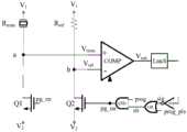
图1为本实施例提供的自关断电路的电路图。如图1所示,所述自关断电路与一编程电路连接,包括参考电路、比较电路及信号传输控制电路。FIG. 1 is a circuit diagram of a self-shutdown circuit provided in this embodiment. As shown in FIG. 1 , the self-shutdown circuit is connected to a programming circuit, and includes a reference circuit, a comparison circuit and a signal transmission control circuit.
所述编程电路包括阻变存储器Rrram、第一开关管Q1及第一节点a。第一开关管Q1具有第一端、第二端和控制端,所述第一端及所述第二端通常是用于输入/输出的源极和漏极,而所述控制端则是用于控制所述第一开关管Q1开闭的栅极。所述阻变存储器Rrram具有正端和负端,当电流从所述阻变存储器Rrram的正端流向负端时,所述阻变存储器Rrram从高阻态转换为低阻态;反之,当电流从所述阻变存储器Rrram的负端流向正端时,所述阻变存储器Rrram从低阻态转换为高阻态。本实施例中,所述阻变存储器Rrram的正端用于输入第一电压V1,负端与所述第一开关管Q1的第二端连接,所述第一开关管Q1的第一端用于输入第二电压V2。所述第一节点a是所述阻变存储器Rrram的负端与所述第一开关管Q1的第二端的连接中点。The programming circuit includes a resistive memory Rrram , a first switch transistor Q1 and a first node a. The first switch tube Q1 has a first end, a second end and a control end, the first end and the second end are usually the source and drain for input/output, and the control end is used for input/output. The gate is used to control the opening and closing of the first switch transistor Q1. The resistive memory Rrram has a positive terminal and a negative terminal. When the current flows from the positive terminal of the resistive memory Rrram to the negative terminal, the resistive memory Rrram is converted from a high resistance state to a low resistance state; otherwise , when the current flows from the negative terminal of the resistive variable memory Rrram to the positive terminal, the resistive variable memory Rrram is converted from a low resistance state to a high resistance state. In this embodiment, the positive terminal of the resistive variable memory Rrram is used to input the first voltage V1 , and the negative terminal is connected to the second terminal of the first switching transistor Q1, and the first switching transistor Q1 has a first The terminal is used to input the second voltage V2 . The first node a is the midpoint of the connection between the negative terminal of the resistive memory Rrram and the second terminal of the first switch transistor Q1.
所述参考电路包括参考电阻Rref、第二开关管Q2及第二节点b。第二开关管Q2也具有第一端、第二端和控制端,同理,所述第一端及所述第二端通常是用于输入/输出的源极和漏极,而所述控制端则是用于控制所述第二开关管Q2开闭的栅极。所述参考电阻Rref为定值电阻,其具有第一端和第二端,所述参考电阻Rref的第一端用于输入所述第一电压V1,第二端与所述第二开关管Q2的第二端连接,所述第二开关管Q2的第一端用于输入所述第二电压V2,所述第二节点b是所述参考电阻Rref的第二端与所述第二开关管Q2的第二端的连接中点。The reference circuit includes a reference resistor Rref , a second switch transistor Q2 and a second node b. The second switch Q2 also has a first end, a second end and a control end. Similarly, the first end and the second end are usually the source and drain for input/output, and the control The terminal is the gate used to control the opening and closing of the second switch transistor Q2. The reference resistor Rref is a constant-value resistor with a first end and a second end. The first end of the reference resistor Rref is used to input the first voltage V1 , and the second end is connected to the second end. The second end of the switch tube Q2 is connected, the first end of the second switch tube Q2 is used to input the second voltage V2 , the second node b is the second end of the reference resistor Rref and the The connection midpoint of the second end of the second switch tube Q2.
应理解,所述阻变存储器Rrram的正端和负端不限于是图1中的连接方式,还可以是所述阻变存储器Rrram的正端与所述第一开关管Q1的第二端连接,所述负端用于输入所述第一电压V1。所述第一节点a和所述第二节点b也不限于是两个器件之间的连接中点,可以是两个器件相连接的端部之间的任意一点,本发明不作限制。It should be understood that the positive terminal and the negative terminal of the resistive memory Rrram are not limited to the connection mode shown in FIG. 1 , but may also be the positive terminal of the resistive memory Rrram and the second terminal of the first switch transistor Q1 terminal is connected, and the negative terminal is used for inputting the first voltage V1 . The first node a and the second node b are also not limited to be the connection midpoint between the two devices, but may be any point between the connected ends of the two devices, which is not limited in the present invention.
进一步,所述比较电路包括一比较器COMP,所述比较器COMP具有正向输入端、反向输入端、输出端和控制端,所述正向输入端与所述反向输入端用于输入需要进行比较的信号,所述控制端用于控制所述比较器COMP的开闭,所述比较器COMP的正向输入端和反向输入端作为所述比较电路的输入端,所述比较器COMP的输出端作为所述比较电路的输出端,所述比较器COMP的控制端作为所述比较电路的控制端。本实施例中,所述比较器COMP的正向输入端与所述第一节点a连接,反向输入端与所述第二节点b,当所述阻变存储器Rrram的正端及所述参考电阻Rref的第一端同时输入所述第一电压V1并且所述第一开关管Q1的第一端及所述第二开关管Q2的第一端同时输入所述第二电压V2时(第一电压V1与所述第二电压V2不相等),所述第一节点a与所述第二节点b分别将所述编程通路和所述参考通路上的中间点电压输入所述比较器COMP中进行比较。为了便于描述,将所述第一节点a上的电压称为编程电压Vrram,所述第二节点b上的电压称为参考电压Vref。所述比较器COMP对所述编程电压Vrram和所述参考电压Vref进行比较,并在输出端输出比较信号Vout,所述比较信号Vout用于指示所述编程电压Vrram和所述参考电压Vref的大小关系。Further, the comparison circuit includes a comparator COMP, the comparator COMP has a forward input terminal, a reverse input terminal, an output terminal and a control terminal, and the forward input terminal and the reverse input terminal are used for input The signal that needs to be compared, the control terminal is used to control the opening and closing of the comparator COMP, the forward input terminal and the reverse input terminal of the comparator COMP are used as the input terminals of the comparison circuit, the comparator The output terminal of COMP is used as the output terminal of the comparison circuit, and the control terminal of the comparator COMP is used as the control terminal of the comparison circuit. In this embodiment, the forward input terminal of the comparator COMP is connected to the first node a, and the reverse input terminal is connected to the second node b. When the positive terminal of the resistive variable memory Rrram is connected to the first node a The first terminal of the reference resistor Rref simultaneously inputs the first voltage V1 and the first terminal of the first switch transistor Q1 and the first terminal of the second switch transistor Q2 simultaneously input the second voltage V2 When (the first voltage V1 and the second voltage V2 are not equal), the first node a and the second node b respectively input the intermediate point voltage on the programming path and the reference path into all are compared in the comparator COMP. For convenience of description, the voltage on the first node a is referred to as a programming voltage Vrram , and the voltage on the second node b is referred to as a reference voltage Vref . The comparator COMP compares the programming voltage Vrram with the reference voltage Vref , and outputs a comparison signal Vout at an output terminal, the comparison signal Vout is used to indicate the programming voltage Vrram and the reference voltage V ref The magnitude relationship of the reference voltage Vref .
本实施例中,所述参考电阻Rref的电阻值Rr及所述第二开关管Q2的宽长比Dr满足如下关系:In this embodiment, the resistance value Rr of the reference resistor Rref and the width-length ratio Dr of the second switch transistor Q2 satisfy the following relationship:
Rr=N*Ra;Rr =N*Ra ;
Dr=N*Dm;Dr =N*Dm ;
其中,N为大于或等于1的整数,RL为所述阻变存储器在低阻态下的电阻值,RH为所述阻变存储器在高阻态下的电阻值,Ra为介于RL和RH之间的阻值(RL<Ra<RH),Dm为所述第一开关管的宽长比。Wherein, N is an integer greater than or equal to 1,RL is the resistance value of the resistive memory in the low resistance state,RH is the resistance value of the resistive memory in the high resistance state, and Ra is between The resistance value betweenRL andRH (RL <Ra <RH ), Dm is the width-length ratio of the first switch tube.
这样一来,当N大于1时,可以将参考电路上的电流减小N倍,但所述参考电压Vref保持不变,从而可以降低所述自关断电路工作时的功耗。In this way, when N is greater than 1, the current on the reference circuit can be reduced by N times, but the reference voltage Vref remains unchanged, thereby reducing the power consumption when the self-shutdown circuit operates.
可以理解的是,当所述编程电路作为一阻变存储器的存储单元时,需要对所述编程电路进行编程(也就是对所述阻变存储器Rrram进行编程)。所述阻变存储器的常规编程具有两种电压控制方式:当编程是置位(set)时,V1的电压值大于V2的电压值,电流从所述阻变存储器Rrram的正端流向负端,所述阻变存储器Rrram的电阻值从RH变为RL,其中RH>>RL,实现所述存储单元从高阻态向低阻态转换;当编程是复位(reset)时,V1的电压值小于V2的电压值,电流从所述阻变存储器Rrram的负端流向正端,所述阻变存储器Rrram的电阻值从RL变为RH,实现所述存储单元从低阻态到高阻态转换。所述编程电路在进行编程时,当编程为置位时,V1为高电压,所述阻变存储器Rrram开始的电阻值为RH,此时,所述编程电压Vrram小于所述参考电压Vref,当编程完成时,所述阻变存储器Rrram的电阻值变为RL,所述编程电压Vrram大于所述参考电压Vref。相应的,当编程为复位时,V1为低电压,所述阻变存储器Rrram的电阻值开始为RL,所述编程电压Vrram小于所述参考电压Vref,当编程完成时,所述阻变存储器Rrram的电阻值变为RH,所述编程电压Vrram大于所述参考电压Vref。可见,无论在什么状态下,当编程结束时,所述编程电压Vrram都会大于所述参考电压Vref,所以可以将所述编程电压Vrram和参考电压Vref的电压大小作为判定编程完成的标志,也即所述比较器COMP输出的所述比较信号Vout可以用于指示所述编程电路的编程状态。It can be understood that, when the programming circuit is used as a storage unit of a resistive memory, the programming circuit needs to be programmed (that is, the resistive memory Rrram is programmed). The conventional programming of the resistive memory hastwo voltage control methods: when programming is set, the voltage value of V1 is greaterthan the voltage value of V2, and the current flows from the positive terminal of the resistive memory Rrram to the At the negative end, the resistance value of the resistive memory Rrram changes fromRH toRL , whereRH >>RL , which realizes the transition of the memory cell from a high-resistance state to a low-resistance state; when programming is a reset (reset) ), the voltage value of V1 is less than the voltage value of V2 , the current flows from the negative end of the resistive memory Rrram to the positive end, and the resistance value of the resistive memory Rrram changes fromRL toRH . The memory cell transitions from a low resistance state to a high resistance state. When the programming circuit is programming, when the programming is set, V1 is a high voltage, and the resistance value of the resistive memory Rrram is RH , and at this time, the programming voltage Vrram is smaller than the reference voltage Vref , when programming is completed, the resistance value of the resistive memory Rrram becomesRL , and the programming voltage Vrram is greater than the reference voltage Vref . Correspondingly, when programming is reset, V1 is a low voltage, the resistance value of the resistive memory Rrram starts to be RL , the programming voltage Vrram is lower than the reference voltage Vref , when the programming is completed, all The resistance value of the resistive memory Rrram becomes RH , and the programming voltage Vrram is greater than the reference voltage Vref . It can be seen that no matter in what state, when the programming is over, the programming voltage Vrram will be greater than the reference voltage Vref , so the voltages of the programming voltage Vrram and the reference voltage Vref can be used to determine whether the programming is completed. A flag, that is, the comparison signal Vout output by the comparator COMP can be used to indicate the programming state of the programming circuit.
由于所述比较器COMP的正向输入端和反向输入端分别输入所述编程电压Vrram和所述参考电压Vref,所以当所述编程电路正在编程时,所述编程电压Vrram小于所述参考电压Vref,此时所述比较信号Vout为低电平“0”;当所述编程电路完成编程时,所述编程电压Vrram大于所述参考电压Vref,此时所述比较信号Vout为高电平“1”;所以,当所述比较信号Vout从低电平“0”跳转为高电平“1”即是编程完成的标志,以利用所述比较信号Vout来关闭所述编程电路,实现自关断的功能。当然,作为可选实施例,所述比较器COMP的正向输入端和反向输入端还可以分别输入所述参考电压Vref和所述编程电压Vrram,此时,所述当所述编程电压Vrram大于所述参考电压Vref时,所述比较信号Vout为低电平“0”,当所述编程电压Vrram小于所述参考电压Vref时,所述比较信号Vout为高电平“1”,当所述比较信号Vout从高电平“1”跳转为低电平“0”即是编程完成的标志。Since the programming voltage Vrram and the reference voltage Vref are respectively input to the forward input terminal and the reverse input terminal of the comparator COMP, when the programming circuit is programming, the programming voltage Vrram is smaller than the the reference voltage Vref , the comparison signal Vout is at a low level “0” at this time; when the programming circuit completes programming, the programming voltage Vrram is greater than the reference voltage Vref , at this time the comparison The signal Vout is a high level "1"; therefore, when the comparison signal Vout jumps from a low level "0" to a high level "1", it is a sign of programming completion, so that the comparison signal V out can be used.out to close the programming circuit to realize the function of self-shutdown. Of course, as an optional embodiment, the reference voltage Vref and the programming voltage Vrram may also be input to the forward input terminal and the reverse input terminal of the comparator COMP, respectively. When the voltage Vrram is greater than the reference voltage Vref , the comparison signal Vout is at a low level “0”, and when the programming voltage Vrram is lower than the reference voltage Vref , the comparison signal Vout is at a high level The level "1", when the comparison signal Vout jumps from the high level "1" to the low level "0", is a sign that the programming is completed.
进一步,所述信号传输控制电路在一编程信号及所述比较信号Vout的控制下,当所述编程信号指示所述编程电路开始编程时开启所述编程电路、参考电路及比较电路;当所述比较信号Vout指示所述编程电路完成编程时关闭所述编程电路、参考电路及比较电路。Further, under the control of a programming signal and the comparison signal Vout , the signal transmission control circuit turns on the programming circuit, the reference circuit and the comparison circuit when the programming signal instructs the programming circuit to start programming; The comparison signal Vout instructs the programming circuit to turn off the programming circuit, the reference circuit and the comparison circuit when the programming is completed.
图2为本实施例提供的所述自关断电路中关键信号的时序图。具体的,结合图1及图2所示,所述编程信号包括编程时间信号prog及编程脉冲信号prog_pls。所述编程时间信号prog用于指示编程时间T1,通常,为了保证所述编程电路在所述编程时间T1下能够完成编程,所述编程时间信号prog指示的编程时间T1通常需要大于所述编程电路的实际编程时间。本实施例中,当所述编程时间信号prog为高电平“1”时代表所述编程电路的编程时间T1,其余时刻均为低电平“0”。应理解,这个编程时间T1可以是由外部规定的可以留给所述编程电路进行编程的时间。所述编程脉冲信号prog_pls用于在所述编程电路开始编程时提供一短脉冲,也就是说,所述编程脉冲信号prog_pls仅在编程初始时刻为高电平“1”,其余时刻均为低电平“0”。FIG. 2 is a timing diagram of key signals in the self-shutdown circuit provided in this embodiment. Specifically, as shown in FIG. 1 and FIG. 2 , the programming signal includes a programming time signal prog and a programming pulse signal prog_pls. The programming time signal prog is used to indicate the programming time T1. Generally, in order to ensure that the programming circuit can complete programming under the programming time T1, the programming time T1 indicated by the programming time signal prog usually needs to be greater than the programming circuit. actual programming time. In this embodiment, when the programming time signal prog is at a high level of “1”, it represents the programming time T1 of the programming circuit, and the other times are at a low level of “0”. It should be understood that this programming time T1 may be a time specified by the outside that can be reserved for the programming circuit to perform programming. The programming pulse signal prog_pls is used to provide a short pulse when the programming circuit starts programming, that is to say, the programming pulse signal prog_pls is only at a high level “1” at the initial programming time, and is low at the rest of the time. Flat "0".
所述信号传输控制电路包括锁存器Latch、非门NO、或门OR及与门AND。所述锁存器Latch的输入端与所述比较器COMP的输出端连接,所述锁存器Latch的输出端与所述非门NO的输入端连接,所述比较器COMP输出所述比较信号Vout后,所述锁存器Latch可以将所述比较信号Vout锁存并输入所述非门NO中,防止所述比较器COMP在关闭后,所述比较器COMP的输出不能与所述比较信号Vout保持一致的情况。所述非门NO将所述比较信号Vout作非运算后输出sig信号,也即是说,所述sig信号是与所述比较信号Vout的信号相反的信号,所述非门NO的输出端与所述或门OR的一个输入端连接,用于将所述sig信号输入所述或门OR中。所述或门OR的另一输入端输入所述编程脉冲信号prog_pls,所述或门OR将所述sig信号及所述编程脉冲信号prog_pls进行或运算,并输出sir信号,也即是说,所述sir信号是所述sig信号与所述编程脉冲信号prog_pls进行或运算后得到的信号,所述或门OR的输出端与所述与门AND的一输入端连接,用于将所述sir信号输入所述与门AND中。所述与门AND的另一输入端用于输入所述编程时间信号prog,所述与门AND将所述sir信号与所述编程时间信号prog进行与运算,并输出pg_en信号,也即是说,所述pg_en信号是所述sir信号与所述编程时间信号prog进行与运算后得到的信号,所述与门AND的输出端与所述第一开关管Q1、第二开关管Q2及所述比较器COMP的控制端连接,用于将所述pg_en信号输入所述第一开关管Q1、第二开关管Q2及所述比较器COMP中,通过控制所述第一开关管Q1、第二开关管Q2及所述比较器COMP的开闭以控制所述编程电路、参考电路及比较电路的通断。The signal transmission control circuit includes a latch Latch, a NOT gate NO, an OR gate OR, and an AND gate AND. The input end of the latch Latch is connected to the output end of the comparator COMP, the output end of the latch Latch is connected to the input end of the NOT gate NO, and the comparator COMP outputs the comparison signal After Vout , the latch Latch can latch the comparison signal Vout and input it into the NOT gate NO, to prevent the output of the comparator COMP from being unable to match the output of the comparator COMP after it is turned off. Compare the case where the signal Vout remains the same. The NOT gate NO outputs a sig signal after negating the comparison signal Vout , that is to say, the sig signal is a signal opposite to the signal of the comparison signal Vout , and the output of the NOT gate NO The terminal is connected to an input terminal of the OR gate OR, and is used for inputting the sig signal into the OR gate OR. The other input terminal of the OR gate OR inputs the programming pulse signal prog_pls, the OR gate OR performs the OR operation on the sig signal and the programming pulse signal prog_pls, and outputs the sir signal, that is to say, the The sir signal is a signal obtained after the sig signal and the programming pulse signal prog_pls are ORed, and an output end of the OR gate OR is connected to an input end of the AND gate AND for connecting the sir signal input into the AND gate AND. The other input end of the AND gate AND is used to input the programming time signal prog, the AND gate AND performs an AND operation on the sir signal and the programming time signal prog, and outputs the pg_en signal, that is, , the pg_en signal is a signal obtained by AND operation of the sir signal and the programming time signal prog, the output end of the AND gate AND is connected to the first switch Q1, the second switch Q2 and the The control terminal of the comparator COMP is connected to input the pg_en signal into the first switch tube Q1, the second switch tube Q2 and the comparator COMP, by controlling the first switch tube Q1 and the second switch tube The on-off of the transistor Q2 and the comparator COMP is used to control the on-off of the programming circuit, the reference circuit and the comparison circuit.
请继续参阅图1和图2,接下来将阐述所述信号传输控制电路的工作原理。Please continue to refer to FIG. 1 and FIG. 2 , and the working principle of the signal transmission control circuit will be described next.
当所述编程电路未开始编程时,所述编程时间信号prog为低电平“0”时,所述编程脉冲信号prog_pls也为低电平“0”,此时,所述比较信号Vout可以为高电平“1”和低电平“0”,所述sig信号也可以为高电平“1”和低电平“0”,所述sir信号为低电平“0”,所述pg_en信号也为低电平“0”,所述第一开关管Q1、第二开关管Q2及所述比较器COMP都处于关闭状态,所述编程电路、参考电路及比较电路编程电路关闭。When the programming circuit does not start programming, when the programming time signal prog is at a low level of "0", the programming pulse signal prog_pls is also at a low level of "0", and at this time, the comparison signal Vout can be is a high level "1" and a low level "0", the sig signal can also be a high level "1" and a low level "0", the sir signal is a low level "0", the The pg_en signal is also at low level “0”, the first switch Q1 , the second switch Q2 and the comparator COMP are all turned off, and the programming circuit, the reference circuit and the comparison circuit programming circuit are turned off.
当所述编程电路开始编程时,所述编程时间信号prog上跳为高电平“1”,所述编程脉冲信号prog_pls会在编程开始的时刻上跳为高电平“1”,此时,所述比较信号Vout可以为高电平“1”和低电平“0”,所述sig信号也可以为高电平“1”和低电平“0”,所述sir信号为高电平“1”,所述pg_en信号也会跳变为高电平“1”,从而打开所述第一开关管Q1、第二开关管Q2及所述比较器COMP,所述编程电路、参考电路及比较电路开启。所述编程电路开始编程后,所述编程电压Vrram小于所述参考电压Vref,所以所述比较信号Vout为低电平“0”,所述sig信号变为高电平“1”,所述sir信号为高电平“1”,所述pg_en信号也会保持高电平“1”。When the programming circuit starts programming, the programming time signal prog jumps up to a high level "1", and the programming pulse signal prog_pls jumps to a high level "1" at the moment when the programming starts. At this time, The comparison signal Vout can be a high level "1" and a low level "0", the sig signal can also be a high level "1" and a low level "0", and the sir signal is a high level. level "1", the pg_en signal will also jump to a high level "1", thereby turning on the first switch Q1, the second switch Q2 and the comparator COMP, the programming circuit, the reference circuit and the comparator circuit is turned on. After the programming circuit starts programming, the programming voltage Vrram is lower than the reference voltage Vref , so the comparison signal Vout is a low level "0", and the sig signal becomes a high level "1", The sir signal is at a high level of "1", and the pg_en signal also remains at a high level of "1".
经过一个非常短的脉冲时间,所述编程脉冲信号prog_pls会跳变为低电平“0”,此时,由于所述sig信号已经处于高电平“1”,所以所述sir信号也处于高电平“1”,所述pg_en信号仍然会保持高电平“1”,整个电路仍然会处于正常的工作状态。在某一个时间点,若所述阻变存储器Rrram的电阻状态发生改变,即编程完成时,所述编程电压Vrram与所述参考电压Vref大小将会转换,所述比较信号Vout也会翻转,跳变为高电平“1”,从而使得所述sig信号变为低电平“0”,相应的,所述sir信号跳变为低电平“0”,所述pg_en信号也会跳变为低电平“0”,从而关闭所述第一开关管Q1、第二开关管Q2及所述比较器COMP,所述编程电路、参考电路及比较电路均关闭,T2为所述编程电路的实际编程时间。最终,当所述编程时间信号prog跳变为低电平“0”时,整个编程周期结束。After a very short pulse time, the programming pulse signal prog_pls will jump to a low level "0". At this time, since the sig signal is already at a high level "1", the sir signal is also at a high level If the level is "1", the pg_en signal will still maintain a high level "1", and the entire circuit will still be in a normal working state. At a certain point in time, if the resistance state of the resistive memory Rrram changes, that is, when programming is completed, the programming voltage Vrram and the reference voltage Vref will be switched, and the comparison signal Vout will also change. It will flip and jump to a high level "1", so that the sig signal becomes a low level "0", correspondingly, the sir signal jumps to a low level "0", and the pg_en signal also will jump to a low level "0", thereby turning off the first switch Q1, the second switch Q2 and the comparator COMP, the programming circuit, the reference circuit and the comparison circuit are all turned off, T2 is the The actual programming time of the programmed circuit. Finally, when the programming time signal prog transitions to a low level "0", the entire programming cycle ends.
可见,所述自关断电路可以在所述编程电路开始编程时自动开启所述编程电路、参考电路及比较电路,在编程完成后自动关闭所述编程电路、参考电路及比较电路,从而在设定的编程时间T1较长的情况下节约所述编程电路在编程完成后的功耗。同时,如果将对所述比较信号Vout或所述pg_en信号进行监控,便可以在外部监测所述编程电路的实际编程时间,从而可以统计出所述编程电路编程的编程时间范围,为后期优化编程时间提供数据支持,从而可以降低预设编程时间,提高编程速度。It can be seen that the self-shutdown circuit can automatically turn on the programming circuit, the reference circuit and the comparison circuit when the programming circuit starts to program, and automatically turn off the programming circuit, the reference circuit and the comparison circuit after the programming is completed, so as to set the When the predetermined programming time T1 is long, the power consumption of the programming circuit after the programming is completed can be saved. At the same time, if the comparison signal Vout or the pg_en signal is to be monitored, the actual programming time of the programming circuit can be monitored externally, so that the programming time range of programming by the programming circuit can be counted for later optimization. The programming time provides data support, so that the preset programming time can be reduced and the programming speed can be increased.
基于此,本实施例还提供了一种半导体存储结构。图3为本实施例提供的半导体存储结构的示意图,如图3所示,所述半导体存储结构包括若干编程电路及若干所述的自关断电路Sec,所述自关断电路Sec用于实现所述编程电路的自关断。具体的,所述编程电路中的阻变存储器构成所述半导体存储结构中的一个存储单元Cell,通常所述阻变存储器呈行列分布,使得所述存储单元Cell也是呈行列分布的,所述编程电路中的第一开关管位于所述半导体存储结构的外围电路中,用于控制所述阻变存储器。图3示意性的展示出了4行6列所述存储单元Cell构成的半导体存储结构。Based on this, this embodiment also provides a semiconductor memory structure. FIG. 3 is a schematic diagram of a semiconductor storage structure provided in this embodiment. As shown in FIG. 3 , the semiconductor storage structure includes a plurality of programming circuits and a plurality of the self-shutdown circuits Sec, and the self-shutdown circuits Sec are used to realize self-shutdown of the programming circuit. Specifically, the resistive memory in the programming circuit constitutes a memory cell Cell in the semiconductor storage structure. Usually, the resistive memory is distributed in rows and columns, so that the memory cells Cell are also distributed in rows and columns. The first switch transistor in the circuit is located in the peripheral circuit of the semiconductor storage structure, and is used for controlling the resistive variable memory. FIG. 3 schematically shows a semiconductor memory structure composed of the memory cells Cell with 4 rows and 6 columns.
每个所述编程电路可以对应一个所述自关断电路Sec,使得每个所述自关断电路Sec可以独立控制一个所述编程电路的自关断。但是由于所述半导体存储结构在编程时,通常都只是单独对一个所述存储单元Cell中的阻变存储器进行编程,为了降低所述半导体存储结构的成本和尺寸,本实施例中,每列所述编程电路对应一个所述自关断电路Sec,也就是说,一列上的所有所述编程电路共用一个所述自关断电路Sec,所述半导体存储结构还包括自关断选通电路(未示出),每列所述编程电路对应一个所述自关断选通电路,所述自关断选通电路可以将所述自关断电路与对应列中的任一所述编程电路选通。Each of the programming circuits may correspond to one of the self-shutdown circuits Sec, so that each of the self-shutdown circuits Sec can independently control the self-shutdown of one of the programming circuits. However, since the semiconductor storage structure usually only programs the resistive memory in one of the storage cells Cell independently during programming, in order to reduce the cost and size of the semiconductor storage structure, in this embodiment, the The programming circuit corresponds to one of the self-shutdown circuits Sec, that is to say, all the programming circuits on a column share one of the self-shutoff circuits Sec, and the semiconductor memory structure further includes a self-shutoff gating circuit (not shown). shown), the programming circuits in each column correspond to one of the self-shutoff gating circuits, and the self-shutoff gating circuit can select the self-shutoff circuit and any one of the programming circuits in the corresponding column. .
具体的,所述半导体存储结构还包括行选通电路和列选通电路,在编程时,所述行选通电路用于选中一行存储单元进行编程,所述列选通电路用于选通一列所述存储单元进行编程,一行存储单元和一列存储单元的交叉点上的存储单元Cell即为需要编程的存储单元,例如若需要选中图3中具有阴影的存储单元Cell进行编程,需要所述行选通电路选中第二行,所述列选通电路选中第三列。进一步,所述自关断选通电路将所述第三列存储单元对应的自关断电路Sec与被选中的所述编程电路选通,此时,所述自关断电路Sec即可实现该编程电路的自关断。Specifically, the semiconductor storage structure further includes a row select circuit and a column select circuit. During programming, the row select circuit is used to select a row of memory cells for programming, and the column select circuit is used to select a column. The memory cell is programmed, and the memory cell Cell on the intersection of a row of memory cells and a column of memory cells is the memory cell to be programmed. For example, if the shaded memory cell Cell in FIG. 3 needs to be selected for programming, the row The gating circuit selects the second row, and the column gating circuit selects the third column. Further, the self-shut-off gating circuit selects the self-shut-off circuit Sec corresponding to the third column of memory cells and the selected programming circuit. At this time, the self-shut-off circuit Sec can realize the Self-shutdown of programming circuits.
本实施例中的所述自关断选通电路、行选通电路和列选通电路均可以是现有技术的任何一种,此处不再过多赘述。应理解,本实施例中仅示意性的展示出多个所述编程电路共用所述自关断电路Sec的一种方式,当所述半导体存储结构的编程模式和/或所述存储单元Cell的分布方式改变时,所述自关断电路Sec的共用方式还可以是其他,在此不在一一举例说明。The self-turn-off gating circuit, the row gating circuit, and the column gating circuit in this embodiment may all be any one of the prior art, which will not be repeated here. It should be understood that this embodiment only schematically shows a way in which multiple programming circuits share the self-shutdown circuit Sec. When the programming mode of the semiconductor memory structure and/or the memory cell Cell When the distribution mode is changed, the shared mode of the self-shutdown circuit Sec may also be other, which will not be illustrated one by one here.
【实施例二】[Example 2]
与实施例一不同的是,本实施例中,所述信号传输控制电路中的或门OR及与门AND的连接方式不同。Different from the first embodiment, in this embodiment, the OR gate OR and the AND gate AND in the signal transmission control circuit are connected differently.
图4为本实施例提供的自关断电路的示意图,如图4所示,本实施例中,所述信号传输控制电路仍然包括锁存器Latch、非门NO、或门OR及与门AND。所述锁存器Latch的输入端与所述比较器COMP的输出端连接,所述锁存器Latch的输出端与所述非门NO的输入端连接,所述比较器COMP输出所述比较信号Vout后,所述锁存器Latch可以将所述比较信号Vout锁存并输入所述非门NO中,防止所述比较器COMP在关闭后,所述比较器COMP的输出不能与所述比较信号Vout保持一致的情况。所述非门NO将所述比较信号Vout作非运算后输出sig信号,也即是说,所述sig信号是与所述比较信号Vout的信号相反的信号,所述非门NO的输出端与所述与门AND的一个输入端连接,用于将所述sig信号输入所述与门AND中。所述与门AND的另一输入端输入所述编程时间信号prog,所述与门AND将所述sig信号及所述编程时间信号prog进行与运算,并输出sir信号,也即是说,所述sir信号是所述sig信号与所述编程时间信号prog进行与运算后得到的信号,所述与门AND的输出端与所述或门OR的一输入端连接,用于将所述sir信号输入所述或门OR中。所述或门OR的另一输入端用于输入所述编程脉冲信号prog_pls,所述或门OR将所述sir信号与所述编程脉冲信号prog_pls进行或运算,并输出pg_en信号,也即是说,所述pg_en信号是所述sir信号与所述编程脉冲信号prog_pls进行或运算后得到的信号,所述或门OR的输出端与所述第一开关管Q1、第二开关管Q2及所述比较器COMP的控制端连接,用于将所述pg_en信号输入所述第一开关管Q1、第二开关管Q2及所述比较器COMP中,通过控制所述第一开关管Q1、第二开关管Q2及所述比较器COMP的开闭以控制所述编程电路、参考电路及比较电路的通断。FIG. 4 is a schematic diagram of a self-shutdown circuit provided in this embodiment. As shown in FIG. 4 , in this embodiment, the signal transmission control circuit still includes a latch Latch, a NOT gate NO, an OR gate OR, and an AND gate AND . The input end of the latch Latch is connected to the output end of the comparator COMP, the output end of the latch Latch is connected to the input end of the NOT gate NO, and the comparator COMP outputs the comparison signal After Vout , the latch Latch can latch the comparison signal Vout and input it into the NOT gate NO, to prevent the output of the comparator COMP from being unable to match the output of the comparator COMP after it is turned off. Compare the case where the signal Vout remains the same. The NOT gate NO outputs a sig signal after negating the comparison signal Vout , that is to say, the sig signal is a signal opposite to the signal of the comparison signal Vout , and the output of the NOT gate NO The terminal is connected to an input terminal of the AND gate AND, and is used for inputting the sig signal into the AND gate AND. The other input terminal of the AND gate AND inputs the programming time signal prog, the AND gate AND performs an AND operation on the sig signal and the programming time signal prog, and outputs the sir signal, that is to say, the The sir signal is a signal obtained after the sig signal and the programming time signal prog are ANDed, and an output end of the AND gate AND is connected to an input end of the OR gate OR for connecting the sir signal input into the OR gate OR. The other input terminal of the OR gate OR is used for inputting the programming pulse signal prog_pls, the OR gate OR performs an OR operation on the sir signal and the programming pulse signal prog_pls, and outputs the pg_en signal, that is to say , the pg_en signal is a signal obtained after the sir signal and the programming pulse signal prog_pls are ORed, and the output end of the OR gate OR is connected to the first switch Q1, the second switch Q2 and the The control terminal of the comparator COMP is connected to input the pg_en signal into the first switch tube Q1, the second switch tube Q2 and the comparator COMP, by controlling the first switch tube Q1 and the second switch tube The on-off of the transistor Q2 and the comparator COMP is used to control the on-off of the programming circuit, the reference circuit and the comparison circuit.
结合图3和图4,接下来将阐述所述信号传输控制电路的工作原理。3 and 4, the working principle of the signal transmission control circuit will be explained next.
当所述编程电路未开始编程时,所述编程时间信号prog为低电平“0”时,所述编程脉冲信号prog_pls也为低电平“0”,此时,所述比较信号Vout可以为高电平“1”和低电平“0”,所述sig信号也可以为高电平“1”和低电平“0”,所述sir信号为低电平“0”,所述pg_en信号也为低电平“0”,所述第一开关管Q1、第二开关管Q2及所述比较器COMP都处于关闭状态,所述编程电路、参考电路及比较电路编程电路关闭。When the programming circuit does not start programming, when the programming time signal prog is at a low level of "0", the programming pulse signal prog_pls is also at a low level of "0", and at this time, the comparison signal Vout can be is a high level "1" and a low level "0", the sig signal can also be a high level "1" and a low level "0", the sir signal is a low level "0", the The pg_en signal is also at low level “0”, the first switch Q1 , the second switch Q2 and the comparator COMP are all turned off, and the programming circuit, the reference circuit and the comparison circuit programming circuit are turned off.
当所述编程电路开始编程时,所述编程时间信号prog上跳为高电平“1”,所述编程脉冲信号prog_pls会在编程开始的时刻上跳为高电平“1”,此时,所述比较信号Vout可以为高电平“1”和低电平“0”,所述sig信号也可以为高电平“1”和低电平“0”,所述sir信号可以为高电平“1”和低电平“0”,所述pg_en信号也会跳变为高电平“1”,从而打开所述第一开关管Q1、第二开关管Q2及所述比较器COMP,所述编程电路、参考电路及比较电路开启。所述编程电路开始编程后,所述编程电压Vrram小于所述参考电压Vref,所以所述比较信号Vout为低电平“0”,所述sig信号变为高电平“1”,所述sir信号为高电平“1”,所述pg_en信号也会保持高电平“1”。经过一个非常短的脉冲时间,所述编程脉冲信号prog_pls会跳变为低电平“0”,此时,由于所述sir信号已经处于高电平“1”,所述pg_en信号仍然会保持高电平“1”,整个电路仍然会处于正常的工作状态。When the programming circuit starts programming, the programming time signal prog jumps up to a high level "1", and the programming pulse signal prog_pls jumps to a high level "1" at the moment when the programming starts. At this time, The comparison signal Vout can be a high level "1" and a low level "0", the sig signal can also be a high level "1" and a low level "0", and the sir signal can be a high level level "1" and low level "0", the pg_en signal will also jump to a high level "1", thereby turning on the first switch Q1, the second switch Q2 and the comparator COMP , the programming circuit, the reference circuit and the comparison circuit are turned on. After the programming circuit starts programming, the programming voltage Vrram is lower than the reference voltage Vref , so the comparison signal Vout is a low level "0", and the sig signal becomes a high level "1", The sir signal is at a high level of "1", and the pg_en signal also remains at a high level of "1". After a very short pulse time, the programming pulse signal prog_pls will jump to a low level "0", at this time, since the sir signal is already at a high level "1", the pg_en signal will still remain high Level "1", the whole circuit will still be in normal working state.
在某一个时间点,若所述阻变存储器Rrram的电阻状态发生改变,即编程完成时,所述编程电压Vrram与所述参考电压Vref大小将会转换,所述比较信号Vout也会翻转,跳变为高电平“1”,从而使得所述sig信号变为低电平“0”,相应的,所述sir信号跳变为低电平“0”,所述pg_en信号也会跳变为低电平“0”,从而关闭所述第一开关管Q1、第二开关管Q2及所述比较器COMP,所述编程电路、参考电路及比较电路均关闭,T2为所述编程电路的实际编程时间。最终,当所述编程时间信号prog跳变为低电平“0”时,整个编程周期结束。At a certain point in time, if the resistance state of the resistive memory Rrram changes, that is, when programming is completed, the programming voltage Vrram and the reference voltage Vref will be switched, and the comparison signal Vout will also change. It will flip and jump to a high level "1", so that the sig signal becomes a low level "0", correspondingly, the sir signal jumps to a low level "0", and the pg_en signal also will jump to a low level "0", thereby turning off the first switch Q1, the second switch Q2 and the comparator COMP, the programming circuit, the reference circuit and the comparison circuit are all turned off, T2 is the The actual programming time of the programmed circuit. Finally, when the programming time signal prog transitions to a low level "0", the entire programming cycle ends.
应理解,实施例一和实施例二仅示意性的展示出所述信号传输控制电路包含的器件以及控制所述编程电路、参考电路及比较电路的逻辑关系,应理解,本发明中的所述信号传输控制电路不限于实施例一和实施例二中的两种,还可以是其他逻辑电路,只要能够实现相同的逻辑关系即可,在此不再一一举例说明。进一步,实施例一和实施例二中的非门NO在所述编程电压Vrram与所述参考电压Vref分别接入所述比较器COMP的反向输入端和正向输入端时可以省略。It should be understood that Embodiment 1 and
综上,在本发明实施例提供自关断电路与一编程电路连接,包括参考电路、比较电路及信号传输控制电路,所述编程电路向所述比较电路输入编程电压,所述参考电路向所述比较电路输入参考电压,所述比较电路可以输出用于指示所述编程电路的编程状态的比较信号,所述信号传输控制电路在一编程信号及所述比较信号的控制下,当所述编程信号指示所述编程电路开始编程时开启所述编程电路、参考电路及比较电路;当所述比较信号指示所述编程电路完成编程时关闭所述编程电路、参考电路及比较电路,从而实现了所述编程电路的自动开启和关断,消除编程完成后的不必要功耗;并且,由于所述比较信号可以指示所述编程电路的编程状态,通过检测所述比较信号即可监测所述编程电路的实际编程时间,从而可以重新优化设计所述编程电路的编程时间,从而提高编程速度。基于此,本发明还提供了一种半导体存储结构。To sum up, the embodiments of the present invention provide a self-shutdown circuit connected to a programming circuit, including a reference circuit, a comparison circuit, and a signal transmission control circuit, the programming circuit inputs a programming voltage to the comparison circuit, and the reference circuit sends a programming voltage to the reference circuit. The comparison circuit inputs a reference voltage, the comparison circuit can output a comparison signal for indicating the programming state of the programming circuit, and the signal transmission control circuit is controlled by a programming signal and the comparison signal, when the programming When the signal instructs the programming circuit to start programming, the programming circuit, the reference circuit and the comparison circuit are turned on; when the comparison signal instructs the programming circuit to complete the programming, the programming circuit, the reference circuit and the comparison circuit are turned off, thereby realizing the Automatic turn-on and turn-off of the programming circuit eliminates unnecessary power consumption after programming is completed; and, since the comparison signal can indicate the programming state of the programming circuit, the programming circuit can be monitored by detecting the comparison signal Therefore, the programming time of the programming circuit can be re-optimized to improve the programming speed. Based on this, the present invention also provides a semiconductor memory structure.
上述仅为本发明的优选实施例而已,并不对本发明起到任何限制作用。任何所属技术领域的技术人员,在不脱离本发明的技术方案的范围内,对本发明揭露的技术方案和技术内容做任何形式的等同替换或修改等变动,均属未脱离本发明的技术方案的内容,仍属于本发明的保护范围之内。The above are only preferred embodiments of the present invention, and do not have any limiting effect on the present invention. Any person skilled in the art, within the scope of not departing from the technical solution of the present invention, makes any form of equivalent replacement or modification to the technical solution and technical content disclosed in the present invention, all belong to the technical solution of the present invention. content still falls within the protection scope of the present invention.
Claims (10)
Translated fromChinesePriority Applications (1)
| Application Number | Priority Date | Filing Date | Title |
|---|---|---|---|
| CN202010102523.2ACN111326201B (en) | 2020-02-19 | 2020-02-19 | Self-turn-off circuit and semiconductor storage structure |
Applications Claiming Priority (1)
| Application Number | Priority Date | Filing Date | Title |
|---|---|---|---|
| CN202010102523.2ACN111326201B (en) | 2020-02-19 | 2020-02-19 | Self-turn-off circuit and semiconductor storage structure |
Publications (2)
| Publication Number | Publication Date |
|---|---|
| CN111326201Atrue CN111326201A (en) | 2020-06-23 |
| CN111326201B CN111326201B (en) | 2023-06-09 |
Family
ID=71172745
Family Applications (1)
| Application Number | Title | Priority Date | Filing Date |
|---|---|---|---|
| CN202010102523.2AActiveCN111326201B (en) | 2020-02-19 | 2020-02-19 | Self-turn-off circuit and semiconductor storage structure |
Country Status (1)
| Country | Link |
|---|---|
| CN (1) | CN111326201B (en) |
Citations (6)
| Publication number | Priority date | Publication date | Assignee | Title |
|---|---|---|---|---|
| US20040114444A1 (en)* | 2002-12-04 | 2004-06-17 | Sharp Kabushiki Kaisha | Semiconductor memory device and method for programming and erasing a memory cell |
| US20040160798A1 (en)* | 2002-10-31 | 2004-08-19 | Unity Semiconductor Inc. | Adaptive programming technique for a re-writable conductive memory device |
| US8441266B1 (en)* | 2009-08-07 | 2013-05-14 | Altera Corporation | Sensing circuit |
| CN104036824A (en)* | 2013-03-06 | 2014-09-10 | 索尼公司 | Semiconductor Device And Information Reading Method |
| US20180061466A1 (en)* | 2016-08-30 | 2018-03-01 | SK Hynix Inc. | Semiconductor memory system and operating method thereof |
| US20190066778A1 (en)* | 2017-08-28 | 2019-02-28 | Macronix International Co., Ltd. | Phase change memory apparatus and read control method to reduce read disturb and sneak current phenomena |
- 2020
- 2020-02-19CNCN202010102523.2Apatent/CN111326201B/enactiveActive
Patent Citations (6)
| Publication number | Priority date | Publication date | Assignee | Title |
|---|---|---|---|---|
| US20040160798A1 (en)* | 2002-10-31 | 2004-08-19 | Unity Semiconductor Inc. | Adaptive programming technique for a re-writable conductive memory device |
| US20040114444A1 (en)* | 2002-12-04 | 2004-06-17 | Sharp Kabushiki Kaisha | Semiconductor memory device and method for programming and erasing a memory cell |
| US8441266B1 (en)* | 2009-08-07 | 2013-05-14 | Altera Corporation | Sensing circuit |
| CN104036824A (en)* | 2013-03-06 | 2014-09-10 | 索尼公司 | Semiconductor Device And Information Reading Method |
| US20180061466A1 (en)* | 2016-08-30 | 2018-03-01 | SK Hynix Inc. | Semiconductor memory system and operating method thereof |
| US20190066778A1 (en)* | 2017-08-28 | 2019-02-28 | Macronix International Co., Ltd. | Phase change memory apparatus and read control method to reduce read disturb and sneak current phenomena |
Also Published As
| Publication number | Publication date |
|---|---|
| CN111326201B (en) | 2023-06-09 |
Similar Documents
| Publication | Publication Date | Title |
|---|---|---|
| US8031516B2 (en) | Writing memory cells exhibiting threshold switch behavior | |
| US5331220A (en) | Soft wakeup output buffer | |
| CN107305783B (en) | Memory device and method for bipolar operation | |
| KR20040041069A (en) | Semiconductor memory device and control method thereof | |
| US11232836B2 (en) | Resistive random access memory device | |
| US10855288B2 (en) | Logic design with unipolar memristors | |
| CN110797063A (en) | Memristor memory chip and operation method thereof | |
| US8446754B2 (en) | Semiconductor memory apparatus and method of driving the same | |
| CN115831190B (en) | Self-write-stop operation circuit and self-write-stop operation method of memristor | |
| CN111326201A (en) | Self-turn-off circuit and semiconductor memory structure | |
| CN113676176A (en) | Logic gate circuit | |
| CN110827897B (en) | Over-write prevention circuit and method of memristor | |
| CN113110676A (en) | Circuit structure for reducing LDO surge current through step-by-step starting | |
| US5650672A (en) | High-voltage power multiplexor | |
| CN101281790A (en) | Design Method of Control Circuit with Adjustable Pulse Width for Phase Change Memory Read and Write Operations | |
| US11437101B2 (en) | Resistive memory storage apparatus and operating method thereof | |
| CN117636959A (en) | Driving circuit, memory device and method of operating the same | |
| CN109509496B (en) | How to operate a resistive memory element | |
| CN105869672A (en) | RRAM-based nonvolatile FPGA programmed point circuit and operating method thereof | |
| JP6638628B2 (en) | Gate drive | |
| USRE45200E1 (en) | Programmable signal routing systems having low static leakage | |
| TWI885864B (en) | Control device, control method and memory system | |
| WO2025113484A1 (en) | Drive circuit, and memory device and operation method therefor | |
| CN118465603A (en) | A power supply change detection circuit | |
| CN1979681A (en) | Low power read reference circuit for split-gate flash memory |
Legal Events
| Date | Code | Title | Description |
|---|---|---|---|
| PB01 | Publication | ||
| PB01 | Publication | ||
| SE01 | Entry into force of request for substantive examination | ||
| SE01 | Entry into force of request for substantive examination | ||
| GR01 | Patent grant | ||
| GR01 | Patent grant |