CN111326089A - Test fixtures and test systems - Google Patents
Test fixtures and test systemsDownload PDFInfo
- Publication number
- CN111326089A CN111326089ACN201911264355.0ACN201911264355ACN111326089ACN 111326089 ACN111326089 ACN 111326089ACN 201911264355 ACN201911264355 ACN 201911264355ACN 111326089 ACN111326089 ACN 111326089A
- Authority
- CN
- China
- Prior art keywords
- test
- power
- touch
- pad
- voltage
- Prior art date
- Legal status (The legal status is an assumption and is not a legal conclusion. Google has not performed a legal analysis and makes no representation as to the accuracy of the status listed.)
- Granted
Links
Images


Classifications
- G—PHYSICS
- G06—COMPUTING OR CALCULATING; COUNTING
- G06F—ELECTRIC DIGITAL DATA PROCESSING
- G06F3/00—Input arrangements for transferring data to be processed into a form capable of being handled by the computer; Output arrangements for transferring data from processing unit to output unit, e.g. interface arrangements
- G06F3/01—Input arrangements or combined input and output arrangements for interaction between user and computer
- G06F3/03—Arrangements for converting the position or the displacement of a member into a coded form
- G06F3/041—Digitisers, e.g. for touch screens or touch pads, characterised by the transducing means
- G06F3/044—Digitisers, e.g. for touch screens or touch pads, characterised by the transducing means by capacitive means
- G06F3/0445—Digitisers, e.g. for touch screens or touch pads, characterised by the transducing means by capacitive means using two or more layers of sensing electrodes, e.g. using two layers of electrodes separated by a dielectric layer
- G—PHYSICS
- G01—MEASURING; TESTING
- G01R—MEASURING ELECTRIC VARIABLES; MEASURING MAGNETIC VARIABLES
- G01R27/00—Arrangements for measuring resistance, reactance, impedance, or electric characteristics derived therefrom
- G01R27/02—Measuring real or complex resistance, reactance, impedance, or other two-pole characteristics derived therefrom, e.g. time constant
- G01R27/26—Measuring inductance or capacitance; Measuring quality factor, e.g. by using the resonance method; Measuring loss factor; Measuring dielectric constants ; Measuring impedance or related variables
- G01R27/2605—Measuring capacitance
- G—PHYSICS
- G01—MEASURING; TESTING
- G01R—MEASURING ELECTRIC VARIABLES; MEASURING MAGNETIC VARIABLES
- G01R31/00—Arrangements for testing electric properties; Arrangements for locating electric faults; Arrangements for electrical testing characterised by what is being tested not provided for elsewhere
- G01R31/28—Testing of electronic circuits, e.g. by signal tracer
- G01R31/282—Testing of electronic circuits specially adapted for particular applications not provided for elsewhere
- G01R31/2825—Testing of electronic circuits specially adapted for particular applications not provided for elsewhere in household appliances or professional audio/video equipment
- G—PHYSICS
- G06—COMPUTING OR CALCULATING; COUNTING
- G06F—ELECTRIC DIGITAL DATA PROCESSING
- G06F3/00—Input arrangements for transferring data to be processed into a form capable of being handled by the computer; Output arrangements for transferring data from processing unit to output unit, e.g. interface arrangements
- G06F3/01—Input arrangements or combined input and output arrangements for interaction between user and computer
- G06F3/03—Arrangements for converting the position or the displacement of a member into a coded form
- G06F3/041—Digitisers, e.g. for touch screens or touch pads, characterised by the transducing means
- G06F3/044—Digitisers, e.g. for touch screens or touch pads, characterised by the transducing means by capacitive means
- G—PHYSICS
- G09—EDUCATION; CRYPTOGRAPHY; DISPLAY; ADVERTISING; SEALS
- G09G—ARRANGEMENTS OR CIRCUITS FOR CONTROL OF INDICATING DEVICES USING STATIC MEANS TO PRESENT VARIABLE INFORMATION
- G09G3/00—Control arrangements or circuits, of interest only in connection with visual indicators other than cathode-ray tubes
- G09G3/006—Electronic inspection or testing of displays and display drivers, e.g. of LED or LCD displays
- G—PHYSICS
- G06—COMPUTING OR CALCULATING; COUNTING
- G06F—ELECTRIC DIGITAL DATA PROCESSING
- G06F2203/00—Indexing scheme relating to G06F3/00 - G06F3/048
- G06F2203/041—Indexing scheme relating to G06F3/041 - G06F3/045
- G06F2203/04112—Electrode mesh in capacitive digitiser: electrode for touch sensing is formed of a mesh of very fine, normally metallic, interconnected lines that are almost invisible to see. This provides a quite large but transparent electrode surface, without need for ITO or similar transparent conductive material
- G—PHYSICS
- G06—COMPUTING OR CALCULATING; COUNTING
- G06F—ELECTRIC DIGITAL DATA PROCESSING
- G06F3/00—Input arrangements for transferring data to be processed into a form capable of being handled by the computer; Output arrangements for transferring data from processing unit to output unit, e.g. interface arrangements
- G06F3/01—Input arrangements or combined input and output arrangements for interaction between user and computer
- G06F3/03—Arrangements for converting the position or the displacement of a member into a coded form
- G06F3/041—Digitisers, e.g. for touch screens or touch pads, characterised by the transducing means
- G06F3/044—Digitisers, e.g. for touch screens or touch pads, characterised by the transducing means by capacitive means
- G06F3/0443—Digitisers, e.g. for touch screens or touch pads, characterised by the transducing means by capacitive means using a single layer of sensing electrodes
- G—PHYSICS
- G06—COMPUTING OR CALCULATING; COUNTING
- G06F—ELECTRIC DIGITAL DATA PROCESSING
- G06F3/00—Input arrangements for transferring data to be processed into a form capable of being handled by the computer; Output arrangements for transferring data from processing unit to output unit, e.g. interface arrangements
- G06F3/01—Input arrangements or combined input and output arrangements for interaction between user and computer
- G06F3/03—Arrangements for converting the position or the displacement of a member into a coded form
- G06F3/041—Digitisers, e.g. for touch screens or touch pads, characterised by the transducing means
- G06F3/044—Digitisers, e.g. for touch screens or touch pads, characterised by the transducing means by capacitive means
- G06F3/0446—Digitisers, e.g. for touch screens or touch pads, characterised by the transducing means by capacitive means using a grid-like structure of electrodes in at least two directions, e.g. using row and column electrodes
- G—PHYSICS
- G09—EDUCATION; CRYPTOGRAPHY; DISPLAY; ADVERTISING; SEALS
- G09G—ARRANGEMENTS OR CIRCUITS FOR CONTROL OF INDICATING DEVICES USING STATIC MEANS TO PRESENT VARIABLE INFORMATION
- G09G2354/00—Aspects of interface with display user
Landscapes
- Engineering & Computer Science (AREA)
- Physics & Mathematics (AREA)
- General Physics & Mathematics (AREA)
- Theoretical Computer Science (AREA)
- General Engineering & Computer Science (AREA)
- Computer Hardware Design (AREA)
- Human Computer Interaction (AREA)
- Multimedia (AREA)
- Devices For Indicating Variable Information By Combining Individual Elements (AREA)
- Electroluminescent Light Sources (AREA)
Abstract
Description
Translated fromChinese本申请要求于2018年12月13日提交的第10-2018-0161103号韩国专利申请的优先权和权益,该韩国专利申请出于所有目的通过引用包含于此,如在这里充分地阐述一样。This application claims priority to and the benefit of Korean Patent Application No. 10-2018-0161103, filed on December 13, 2018, which is hereby incorporated by reference for all purposes as if fully set forth herein.
技术领域technical field
发明的示例性实施例总体上涉及显示/触摸面板测试,更具体地,涉及可以在测试触摸感测单元的步骤中测量显示面板的电容的一种测试装置和一种测试系统。Exemplary embodiments of the invention relate generally to display/touch panel testing, and more particularly, to a testing apparatus and a testing system that can measure capacitance of a display panel in the step of testing a touch sensing unit.
背景技术Background technique
本公开涉及一种用于测试显示模块的装置,具体涉及一种用于测试具有触摸感测单元的显示模块的装置。The present disclosure relates to an apparatus for testing a display module, in particular to an apparatus for testing a display module with a touch sensing unit.
有机发光显示装置包括用于显示图像并作为自发光器件的有机发光二极管,并且由于有机发光显示装置的优异的亮度和颜色纯度特性,其正在成为下一代显示装置。有机发光显示装置包括构成显示面板并显示彩色图像的红色像素、绿色像素和蓝色像素。Organic light emitting display devices include organic light emitting diodes for displaying images and as self-luminous devices, and are emerging as next-generation display devices due to their excellent brightness and color purity characteristics. The organic light emitting display device includes red pixels, green pixels, and blue pixels that constitute a display panel and display a color image.
有机发光显示装置包括用于显示图像的包含显示面板的显示模块和被构造为感测外部输入并输出关于外部输入的位置或强度的信息的触摸感测单元。制造有机发光显示装置的工艺包括测试有机发光显示装置的显示模块是否可以正常操作的步骤。The organic light emitting display device includes a display module including a display panel for displaying an image and a touch sensing unit configured to sense an external input and output information on a position or intensity of the external input. The process of manufacturing an organic light emitting display device includes a step of testing whether a display module of the organic light emitting display device can operate normally.
在此背景技术部分中公开的以上信息仅用于对发明构思的背景的理解,因此,其可能会包含不构成现有技术的信息。The above information disclosed in this Background section is only for understanding of the background of the inventive concepts and therefore it may contain information that does not form the prior art.
发明内容SUMMARY OF THE INVENTION
发明构思的实施例提供了可以在测试触摸感测单元的步骤中测量显示面板的电容的一种测试装置和一种测试系统。Embodiments of the inventive concept provide a testing apparatus and a testing system that can measure capacitance of a display panel in a step of testing a touch sensing unit.
发明构思的附加特征将在下面的描述中进行阐述,并且部分地将通过该描述而明显,或者可以通过发明构思的实践而被获知。Additional features of the inventive concepts will be set forth in the description that follows, and in part will be apparent from the description, or may be learned by practice of the inventive concepts.
根据发明构思的示例性实施例,一种测试装置可以包括:触摸测试垫,电连接到显示模块的触摸垫;第一电力测试垫和第二电力测试垫,分别电连接到显示模块的第一电力垫和第二电力垫;电压产生器,将第一测试电力电压和第二测试电力电压分别提供到第一电力测试垫和第二电力测试垫;以及电容测量电路,测量第一电力测试垫与第二电力测试垫之间的电容。According to an exemplary embodiment of the inventive concept, a test apparatus may include: a touch test pad electrically connected to a touch pad of a display module; and a first power test pad and a second power test pad electrically connected to the first power test pad of the display module, respectively a power pad and a second power pad; a voltage generator to provide the first test power voltage and the second test power voltage to the first power test pad and the second power test pad, respectively; and a capacitance measurement circuit to measure the first power test pad Capacitance with the second power test pad.
电压产生器可以响应于电压控制信号而改变第一测试电力电压和第二测试电力电压中的至少一者的电压电平。The voltage generator may vary the voltage level of at least one of the first test power voltage and the second test power voltage in response to the voltage control signal.
测试装置还可以包括:连接件,将触摸垫电连接到触摸测试垫并且将第一电力垫和第二电力垫分别电连接到第一电力测试垫和第二电力测试垫;以及接口,响应于从外部接收的测试控制信号而输出电压控制信号。The test apparatus may further include: a connector electrically connecting the touch pad to the touch test pad and electrically connecting the first power pad and the second power pad to the first power test pad and the second power test pad, respectively; and an interface responsive to The voltage control signal is output from the test control signal received from the outside.
电容测量电路可以输出与测量的电容对应的电容感测信号。The capacitance measurement circuit may output a capacitance sensing signal corresponding to the measured capacitance.
测试装置还可以包括将触摸测试信号输出到触摸测试垫的触摸测试器。The test apparatus may further include a touch tester that outputs a touch test signal to the touch test pad.
触摸测试器输出触摸测试信号的操作和电压产生器输出第一测试电力电压和第二测试电力电压的操作可以并行地执行。The operation of the touch tester to output the touch test signal and the operation of the voltage generator to output the first test power voltage and the second test power voltage may be performed in parallel.
触摸测试垫、第一电力测试垫和第二电力测试垫、电压产生器以及电容测量电路可以设置为单个集成电路。The touch test pad, the first and second power test pads, the voltage generator and the capacitance measurement circuit may be provided as a single integrated circuit.
测试装置还可以包括将面板测试信号输出到显示模块的信号垫的面板测试电路。信号垫包括第一电力垫和第二电力垫。The test apparatus may further include a panel test circuit that outputs a panel test signal to a signal pad of the display module. The signal pad includes a first power pad and a second power pad.
面板测试电路可以包括:显示面板测试垫,电连接到显示模块的信号垫;以及测试信号产生电路,将面板测试信号输出到显示面板测试垫。显示面板测试垫包括第一电力测试垫和第二电力测试垫。The panel test circuit may include: a display panel test pad electrically connected to a signal pad of the display module; and a test signal generation circuit, which outputs the panel test signal to the display panel test pad. The display panel test pads include a first power test pad and a second power test pad.
根据发明构思的示例性实施例,一种测试系统可以包括显示模块和测试装置。显示模块可以包括:显示面板,包括显示区域和与显示区域相邻的非显示区域;以及触摸感测单元,设置在显示面板上以感测施加到触摸感测单元的与显示区域叠置的感测区域的外部输入。显示面板可以包括:触摸垫,设置在非显示区域中并且电连接到触摸感测单元;以及第一电力垫和第二电力垫,设置在非显示区域中并且电连接到显示面板。测试装置可以包括:触摸测试垫,电连接到触摸垫;第一电力测试垫和第二电力测试垫,分别电连接到第一电力垫和第二电力垫;电压产生器,将第一测试电力电压和第二测试电力电压分别提供到第一电力测试垫和第二电力测试垫;以及电容测量电路,测量第一电力测试垫与第二电力测试垫之间的电容。According to an exemplary embodiment of the inventive concept, a testing system may include a display module and a testing apparatus. The display module may include: a display panel including a display area and a non-display area adjacent to the display area; and a touch sensing unit disposed on the display panel to sense a sense applied to the touch sensing unit overlapping the display area external input to the measurement area. The display panel may include: a touch pad disposed in the non-display area and electrically connected to the touch sensing unit; and first and second power pads disposed in the non-display area and electrically connected to the display panel. The test device may include: a touch test pad, electrically connected to the touch pad; a first power test pad and a second power test pad, respectively electrically connected to the first power pad and the second power pad; and a voltage generator to convert the first test power The voltage and the second test power voltage are supplied to the first power test pad and the second power test pad, respectively; and a capacitance measurement circuit measures the capacitance between the first power test pad and the second power test pad.
电压产生器可以响应于电压控制信号而改变第一测试电力电压和第二测试电力电压中的至少一者的电压电平。The voltage generator may vary the voltage level of at least one of the first test power voltage and the second test power voltage in response to the voltage control signal.
测试系统还可以包括:连接件,将触摸垫电连接到触摸测试垫并且将显示面板的第一电力垫和第二电力垫分别电连接到第一电力测试垫和第二电力测试垫;以及接口,响应于从外部接收的测试控制信号而输出电压控制信号。The test system may further include: a connector electrically connecting the touch pad to the touch test pad and electrically connecting the first power pad and the second power pad of the display panel to the first power test pad and the second power test pad, respectively; and an interface , which outputs a voltage control signal in response to a test control signal received from the outside.
电容测量电路可以输出与测量的电容对应的电容感测信号。The capacitance measurement circuit may output a capacitance sensing signal corresponding to the measured capacitance.
测试系统还可以包括将触摸测试信号输出到触摸测试垫的触摸测试器。The test system may also include a touch tester that outputs a touch test signal to the touch test pad.
显示面板还可以包括:多个像素,布置在显示区域中并且连接到多条数据线和多条扫描线。多个像素中的至少一个像素可以包括:发光二极管,包括阳极和阴极;第一晶体管,包括接收第一电力电压的第一电极、电连接到发光二极管的阳极的第二电极和栅电极;电容器,包括连接到第一晶体管的第一电极的第一电极和连接到第一晶体管的栅电极的第二电极;以及第二晶体管,包括连接到多条数据线中的对应的一条数据线的第一电极、连接到电容器的第二电极的第二电极和接收第一扫描信号的栅电极。The display panel may further include a plurality of pixels arranged in the display area and connected to a plurality of data lines and a plurality of scan lines. At least one pixel of the plurality of pixels may include: a light emitting diode including an anode and a cathode; a first transistor including a first electrode receiving a first power voltage, a second electrode electrically connected to the anode of the light emitting diode, and a gate electrode; a capacitor , comprising a first electrode connected to a first electrode of the first transistor and a second electrode connected to a gate electrode of the first transistor; and a second transistor comprising a first electrode connected to a corresponding one of the plurality of data lines An electrode, a second electrode connected to the second electrode of the capacitor, and a gate electrode receiving the first scan signal.
第一晶体管的第一电极可以电连接到第一电力垫,并且发光二极管的阴极可以电连接到第二电力垫。The first electrode of the first transistor may be electrically connected to the first power pad, and the cathode of the light emitting diode may be electrically connected to the second power pad.
电容测量电路可以输出与第一晶体管的第一电极与发光二极管的阴极之间的电容对应的电容感测信号。The capacitance measurement circuit may output a capacitance sensing signal corresponding to the capacitance between the first electrode of the first transistor and the cathode of the light emitting diode.
根据发明构思的示例性实施例,公开了一种使用测试装置的测试方法。测试装置可以包括:触摸测试垫,电连接到触摸感测单元的触摸垫;以及第一电力测试垫和第二电力测试垫,分别电连接到显示面板的第一电力垫和第二电力垫。测试方法可以包括:将第一测试电力电压和第二测试电力电压分别提供到第一电力测试垫和第二电力测试垫;以及测量第一电力测试垫与第二电力测试垫之间的电容。According to an exemplary embodiment of the inventive concept, a testing method using a testing apparatus is disclosed. The testing device may include: a touch test pad electrically connected to the touch pad of the touch sensing unit; and first and second power test pads electrically connected to the first and second power pads of the display panel, respectively. The testing method may include: providing the first test power voltage and the second test power voltage to the first power test pad and the second power test pad, respectively; and measuring the capacitance between the first power test pad and the second power test pad.
测试方法还可以包括将触摸测试信号输出到触摸测试垫。The test method may further include outputting a touch test signal to the touch test pad.
测试方法还可以包括输出与测量的电容对应的电容感测信号。The testing method may further include outputting a capacitance sensing signal corresponding to the measured capacitance.
将理解的是,前面的总体描述和下面的详细描述两者是示例性的和说明性的并且意图提供对如要求保护的发明的进一步解释。It is to be understood that both the foregoing general description and the following detailed description are exemplary and explanatory and are intended to provide further explanation of the invention as claimed.
附图说明Description of drawings
附图示出了发明的示例性实施例,并且与描述一起用于解释发明构思,附图被包括以提供对发明的进一步理解,并且被并入本说明书中并构成本说明书的一部分。The accompanying drawings, which illustrate exemplary embodiments of the invention and, together with the description, serve to explain the inventive concept, are included to provide a further understanding of the invention, and are incorporated in and constitute a part of this specification.
图1是示出根据发明构思的示例性实施例的显示模块的透视图。FIG. 1 is a perspective view illustrating a display module according to an exemplary embodiment of the inventive concept.
图2是示出根据示例性实施例的显示模块的剖视图。FIG. 2 is a cross-sectional view illustrating a display module according to an exemplary embodiment.
图3是示出根据示例性实施例的显示面板的平面图。FIG. 3 is a plan view illustrating a display panel according to an exemplary embodiment.
图4是示出根据示例性实施例的像素的等效电路图。FIG. 4 is an equivalent circuit diagram illustrating a pixel according to an exemplary embodiment.
图5是示出根据示例性实施例的触摸感测单元的平面图。FIG. 5 is a plan view illustrating a touch sensing unit according to an exemplary embodiment.
图6是示出根据示例性实施例的触摸测试装置的框图。FIG. 6 is a block diagram illustrating a touch testing apparatus according to an exemplary embodiment.
图7是示出图3中示出的显示面板与图6中示出的触摸测试装置之间的示例连接结构的框图。FIG. 7 is a block diagram showing an example connection structure between the display panel shown in FIG. 3 and the touch test apparatus shown in FIG. 6 .
图8A、图8B和图8C是均示出由图7中示出的第一电力垫与第二电力垫之间的电压差导致的电容的改变的曲线图。FIGS. 8A , 8B, and 8C are graphs each showing a change in capacitance caused by the voltage difference between the first power pad and the second power pad shown in FIG. 7 .
图9是示出根据另一示例性实施例的触摸测试装置的框图。FIG. 9 is a block diagram illustrating a touch testing apparatus according to another exemplary embodiment.
图10是示出图9的触摸测试电路的结构的示例的图。FIG. 10 is a diagram showing an example of the structure of the touch test circuit of FIG. 9 .
图11是示出根据另一示例性实施例的显示模块的透视图。FIG. 11 is a perspective view illustrating a display module according to another exemplary embodiment.
图12是示出图11中示出的显示面板与图6中示出的触摸测试装置之间的示例连接结构的图。FIG. 12 is a diagram showing an example connection structure between the display panel shown in FIG. 11 and the touch test device shown in FIG. 6 .
具体实施方式Detailed ways
在下面的描述中,为了解释的目的,阐述了许多特定细节,以提供对发明的各种示例性实施例或实施方式的彻底理解。如在这里使用的,“实施例”和“实施方式”是作为采用在这里公开的一个或更多个发明构思的装置或方法的非限制性示例的可互换词。然而,明显的是,各种示例性实施例可以在没有这些特定细节的情况下来实施或者用一个或更多个等同布置来实施。在其他情况下,公知结构和装置以框图形式示出,以避免使各种示例性实施例不必要地模糊。此外,各种示例性实施例可以是不同的,但不必是排他的。例如,在不脱离发明构思的情况下,示例性实施例的特定形状、构造和特性可以在另一示例性实施例中使用或实施。In the following description, for the purposes of explanation, numerous specific details are set forth in order to provide a thorough understanding of various exemplary embodiments or implementations of the invention. As used herein, "embodiment" and "implementation" are used interchangeably as non-limiting examples of apparatuses or methods for employing one or more of the inventive concepts disclosed herein. It will be apparent, however, that various exemplary embodiments may be practiced without these specific details or with one or more equivalent arrangements. In other instances, well-known structures and devices are shown in block diagram form in order to avoid unnecessarily obscuring the various exemplary embodiments. Furthermore, the various exemplary embodiments may vary, but are not necessarily exclusive. For example, the particular shapes, configurations and characteristics of an exemplary embodiment may be used or implemented in another exemplary embodiment without departing from the inventive concept.
除非另外说明,否则示出的示例性实施例将被理解为提供在实践中可以以其来实施发明构思的一些方式的变化的细节的示例性特征。因此,除非另外说明,否则在不脱离发明构思的情况下,可以对各种实施例的特征、组件、模块、层、膜、面板、区域和/或方面等(在下文中,单独地或共同地称为“元件”)进行另外组合、分离、互换和/或重新布置。Unless otherwise stated, the illustrated exemplary embodiments are to be understood as providing exemplary features of varying details of some of the ways in which the inventive concepts may be implemented in practice. Thus, unless otherwise stated, features, components, modules, layers, films, panels, regions and/or aspects, etc. of the various embodiments (hereinafter, individually or collectively) may be referred to as "elements") are otherwise combined, separated, interchanged and/or rearranged.
通常提供附图中的交叉阴影线和/或阴影的使用,以使相邻元件之间的边界清晰。如此,除非说明,否则交叉阴影线或阴影的存在或不存在都不表达或表示对元件的具体材料、材料性质、尺寸、比例、示出元件之间的共性和/或任何其他特性、属性、性质等的任何偏好或要求。此外,在附图中,为了清楚和/或描述性的目的,可以夸大元件的尺寸和相对尺寸。当示例性实施例可以不同地实施时,可以以不同于所描述的顺序来执行特定的工艺顺序。例如,可以基本同时执行或者以与所描述的顺序相反的顺序执行两个连续描述的工艺。此外,同样的附图标记表示同样的元件。The use of cross-hatching and/or hatching in the figures is generally provided to clarify boundaries between adjacent elements. As such, unless stated otherwise, the presence or absence of cross-hatching or hatching does not convey or imply specific materials, material properties, dimensions, proportions, commonalities between illustrated elements and/or any other characteristics, properties, any preference or requirement of nature, etc. Furthermore, in the drawings, the size and relative sizes of elements may be exaggerated for clarity and/or descriptive purposes. While example embodiments may be implemented differently, a particular sequence of processes may be performed in a different order than described. For example, two consecutively described processes may be performed substantially concurrently or in the reverse order of that described. Furthermore, the same reference numerals refer to the same elements.
当元件或层被称为“在”另一元件或层“上”、“连接到”或“结合到”另一元件或层时,该元件或层可以直接在所述另一元件或层上、直接连接到或直接结合到所述另一元件或层,或者可以存在中间元件或中间层。然而,当元件或层被称为“直接在”另一元件或层“上”、“直接连接到”或“直接结合到”另一元件或层时,不存在中间元件或中间层。为此,术语“连接”可以指在存在或不存在中间元件的情况下的物理连接、电连接和/或流体连接。此外,DR1轴、DR2轴和DR3轴不限于诸如x轴、y轴和z轴的直角坐标系的三个轴,并且可以以更宽的含义进行解释。例如,DR1轴、DR2轴和DR3轴可以彼此垂直,或者可以表示彼此不垂直的不同方向。为了本公开的目的,“X、Y和Z中的至少一个(种/者)”和“从由X、Y和Z组成的组中选择的至少一个(种/者)”可以理解为仅X、仅Y、仅Z或者X、Y和Z中的两个(种/者)或更多个(种/者)的任何组合,诸如以XYZ、XYY、YZ和ZZ为例。如在这里使用的,术语“和/或”包括相关所列项中的一个或更多个的任何和全部组合。When an element or layer is referred to as being "on," "connected to," or "bonded to" another element or layer, the element or layer can be directly on the other element or layer , is directly connected or bonded to the other element or layer, or intervening elements or layers may be present. However, when an element or layer is referred to as being "directly on," "directly connected to," or "directly coupled to" another element or layer, there are no intervening elements or layers present. To this end, the term "connected" may refer to a physical, electrical, and/or fluid connection with or without intervening elements. In addition, the DR1 axis, the DR2 axis, and the DR3 axis are not limited to three axes of a rectangular coordinate system such as the x axis, the y axis, and the z axis, and may be interpreted in a broader sense. For example, the DR1, DR2, and DR3 axes may be perpendicular to each other, or may represent different directions that are not perpendicular to each other. For the purpose of this disclosure, "at least one (species/species) of X, Y, and Z" and "at least one (species/species) selected from the group consisting of X, Y, and Z" may be understood to mean only X , Y only, Z only, or any combination of two or more of X, Y, and Z, such as XYZ, XYY, YZ, and ZZ, for example. As used herein, the term "and/or" includes any and all combinations of one or more of the associated listed items.
尽管可以在这里使用术语“第一”、“第二”等来描述各种类型的元件,但是这些元件不应该受这些术语的限制。这些术语用来将一个元件与另一元件区分开来。因此,在不脱离公开的教导的情况下,以下讨论的第一元件可以被称为第二元件。Although the terms "first," "second," etc. may be used herein to describe various types of elements, these elements should not be limited by these terms. These terms are used to distinguish one element from another. Thus, a first element discussed below could be termed a second element without departing from the teachings of the disclosure.
为了描述性目的,在这里可以使用诸如“在……之下”、“在……下方”、“在……下面”、“下”、“在……上方”、“上”、“在……之上”、“较高的”、“侧”(例如,如在“侧壁”中)等的空间相对术语,并且由此来描述如附图中示出的一个元件与另一(其他)元件的关系。空间相对术语意图包括除了附图中描绘的方位之外的设备在使用、操作和/或制造中的不同方位。例如,如果附图中的设备被翻转,则被描述为“在”其他元件或特征“下方”或“之下”的元件将随后被定位为“在”所述其他元件或特征“上方”。因此,示例性术语“在……下方”可以包括上方和下方两种方位。此外,设备可以被另外定位(例如,旋转90度或者在其他方位处),如此,相应地解释在这里使用的空间相对描述语。For descriptive purposes, expressions such as "under", "under", "under", "under", "above", "on", "under" may be used herein. Spatially relative terms such as "above", "higher", "side" (eg, as in "sidewall"), etc., and thereby describe one element as ) element relationship. Spatially relative terms are intended to include different orientations of the device in use, operation, and/or manufacture in addition to the orientation depicted in the figures. For example, if the device in the figures is turned over, elements described as "below" or "beneath" other elements or features would then be oriented "above" the other elements or features. Thus, the exemplary term "below" can encompass both an orientation of above and below. In addition, the device may be otherwise oriented (eg, rotated 90 degrees or at other orientations) and, as such, the spatially relative descriptors used herein should be interpreted accordingly.
在这里使用的术语是出于描述具体实施例的目的,而不意图成为限制。如在这里所使用的,除非上下文另外清楚地指出,否则单数形式“一”、“一个(种/者)”和“所述(该)”也意图包括复数形式。此外,当在本说明书中使用术语“包括”和/或“包含”时,说明存在所陈述的特征、整体、步骤、操作、元件、组件和/或它们的组,但不排除存在或附加一个或更多个其他特征、整体、步骤、操作、元件、组件和/或它们的组。还要注意的是,如在这里使用的,术语“基本上”、“大约”和其他类似的术语被用作近似术语而不是用作程度术语,如此,它们被用来解释将由本领域普通技术人员认识到的测量值、计算值和/或提供值中的固有偏差。The terminology used herein is for the purpose of describing particular embodiments and is not intended to be limiting. As used herein, the singular forms "a", "an" and "the" are intended to include the plural forms as well, unless the context clearly dictates otherwise. Furthermore, when the terms "comprising" and/or "comprising" are used in this specification, it indicates the presence of stated features, integers, steps, operations, elements, components and/or groups thereof, but does not preclude the presence or addition of a or more other features, integers, steps, operations, elements, components and/or groups thereof. Note also that, as used herein, the terms "substantially," "approximately," and other similar terms are used as terms of approximation rather than terms of degree, and as such, they are used to Person-recognized inherent bias in measured, calculated, and/or provided values.
在这里参照作为理想化示例性实施例和/或中间结构的示意图的剖视图来描述各种示例性实施例。如此,预计出现例如由制造技术和/或公差引起的图示的形状的变化。因此,这里公开的示例性实施例不应必然被解释为局限于区域的具体示出的形状,而包括由例如制造引起的形状偏差。以这种方式,图中示出的区域本质上可以是示意性的,且这些区域的形状可以不反映装置的区域的实际形状,如此,不必意图成为限制。Various exemplary embodiments are described herein with reference to cross-sectional illustrations that are schematic illustrations of idealized exemplary embodiments and/or intermediate structures. As such, variations in the shapes of the illustrations due, for example, to manufacturing techniques and/or tolerances, are expected. Thus, the exemplary embodiments disclosed herein should not necessarily be construed as limited to the specifically illustrated shapes of regions, but to include deviations in shapes resulting from, for example, manufacturing. In this manner, the regions illustrated in the figures may be schematic in nature and their shapes may not reflect the actual shape of a region of a device and, as such, are not necessarily intended to be limiting.
如本领域中惯常的,一些示例性实施例用功能块、单元和/或模块来描述并在附图中示出。本领域技术人员将理解的是,这些功能块、单元和/或模块通过诸如逻辑电路的电子(或光学)电路、离散组件、微处理器、硬线电路、存储器元件、布线连接等物理地实施,其可以利用基于半导体的制造技术或其他制造技术来形成。在通过微处理器或其他类似的硬件来实施功能块、单元和/或模块的情况下,可以利用软件(例如,微代码)对它们进行编程和控制,以执行在此所讨论的各种功能,并且可以可选地通过固件和/或软件来驱动它们。还想到的是,每个功能块、单元和/或模块可以通过专用硬件实施,或者作为执行一些功能的专用硬件和执行其他功能的处理器(例如,一个或更多个编程的微处理器和相关电路)的组合来实施。此外,在不脱离发明构思的范围的情况下,一些示例性实施例的每个功能块、单元和/或模块可以物理地分离成两个或更多个交互的且离散的功能块、单元和/或模块。此外,在不脱离发明构思的范围的情况下,一些示例性实施例的功能块、单元和/或模块可以物理地组合成更复杂的功能块、单元和/或模块。As is customary in the art, some exemplary embodiments are described in terms of functional blocks, units and/or modules and are illustrated in the accompanying drawings. It will be understood by those skilled in the art that these functional blocks, units and/or modules are physically implemented by electronic (or optical) circuits such as logic circuits, discrete components, microprocessors, hard-wired circuits, memory elements, wired connections, etc. , which may be formed using semiconductor-based fabrication techniques or other fabrication techniques. Where functional blocks, units and/or modules are implemented by a microprocessor or other similar hardware, they may be programmed and controlled by software (eg, microcode) to perform the various functions discussed herein , and can optionally be driven by firmware and/or software. It is also contemplated that each functional block, unit and/or module may be implemented by special purpose hardware, or as special purpose hardware to perform some functions and a processor (eg, one or more programmed microprocessors and related circuits) are implemented. Furthermore, each functional block, unit and/or module of some exemplary embodiments may be physically separated into two or more interacting and discrete functional blocks, units and/or modules without departing from the scope of the inventive concepts. / or modules. Furthermore, the functional blocks, units and/or modules of some exemplary embodiments may be physically combined into more complex functional blocks, units and/or modules without departing from the scope of the inventive concepts.
除非另外定义,否则在这里使用的所有术语(包括技术术语和科学术语)具有与本公开是其一部分的领域的普通技术人员所通常理解的意思相同的意思。术语(诸如在通用字典中定义的术语)应该被解释为具有与相关领域的上下文中它们的意思一致的意思,而不应以理想化的或过于形式化的含义来解释,除非这里明确地如此定义。Unless otherwise defined, all terms (including technical and scientific terms) used herein have the same meaning as commonly understood by one of ordinary skill in the art to which this disclosure is a part. Terms (such as those defined in general dictionaries) should be construed to have meanings consistent with their meanings in the context of the relevant art, and not to idealized or overly formalized meanings, unless explicitly so definition.
图1是示出根据发明构思的示例性实施例的显示模块DM的透视图。图2是示出根据发明构思的示例性实施例的显示模块DM的剖视图。FIG. 1 is a perspective view illustrating a display module DM according to an exemplary embodiment of the inventive concept. FIG. 2 is a cross-sectional view illustrating a display module DM according to an exemplary embodiment of the inventive concept.
如图1中所示,用于显示图像IM的显示表面IS可以与由第一方向轴DR1和第二方向轴DR2限定的平面平行。与显示表面IS正交的方向(即,显示模块DM的厚度方向)可以被称为第三方向轴DR3。第三方向轴DR3可以用作用于将每个元件的顶表面或前表面与底表面或后表面区分开来的标准。然而,由第一方向轴DR1、第二方向轴DR2和第三方向轴DR3表示的方向可以是相对的,在实施例中,它们可以改变为表示其他方向。在下文中,第一方向、第二方向和第三方向可以分别是由第一方向轴DR1、第二方向轴DR2和第三方向轴DR3表示的方向,并且将用相同的附图标记来标识。As shown in FIG. 1 , the display surface IS for displaying the image IM may be parallel to the plane defined by the first direction axis DR1 and the second direction axis DR2. A direction orthogonal to the display surface IS (ie, the thickness direction of the display module DM) may be referred to as a third direction axis DR3. The third direction axis DR3 may be used as a criterion for distinguishing the top or front surface from the bottom or rear surface of each element. However, the directions represented by the first direction axis DR1, the second direction axis DR2, and the third direction axis DR3 may be opposite, and in embodiments, they may be changed to represent other directions. Hereinafter, the first direction, the second direction and the third direction may be directions represented by the first direction axis DR1, the second direction axis DR2 and the third direction axis DR3, respectively, and will be identified with the same reference numerals.
在本示例性实施例中,显示模块DM可以是平坦的刚性显示模块。然而,发明构思不限于这样的示例,在实施例中,显示模块DM可以被构造为具有柔性性质。根据本实施例的显示模块DM可以用于大尺寸电子装置(例如,电视机和监视器)或者中小尺寸电子装置(例如,智能电话、平板、汽车导航系统、游戏机和智能手表)。In the present exemplary embodiment, the display module DM may be a flat rigid display module. However, the inventive concept is not limited to such an example, and in an embodiment, the display module DM may be configured to have a flexible property. The display module DM according to the present embodiment can be used for large-sized electronic devices (eg, televisions and monitors) or small and medium-sized electronic devices (eg, smartphones, tablets, car navigation systems, game consoles, and smart watches).
如图1中所示,显示模块DM可以包括其上显示图像IM的显示区域DM-DA和与显示区域DM-DA相邻的非显示区域DM-NDA。非显示区域DM-NDA可以不用于显示图像。在图1中,其中有花的花瓶被示出为图像IM的示例。显示区域DM-DA可以具有矩形或四边形形状。非显示区域DM-NDA可以围绕显示区域DM-DA。然而,发明构思不限于这样的示例,并且可以以相互影响的方式各种地改变显示区域DM-DA的形状和非显示区域DM-NDA的形状。As shown in FIG. 1 , the display module DM may include a display area DM-DA on which the image IM is displayed and a non-display area DM-NDA adjacent to the display area DM-DA. The non-display area DM-NDA may not be used for displaying images. In Figure 1, a vase with flowers in it is shown as an example of an image IM. The display area DM-DA may have a rectangular or quadrangular shape. The non-display area DM-NDA may surround the display area DM-DA. However, the inventive concept is not limited to such an example, and the shape of the display area DM-DA and the shape of the non-display area DM-NDA may be variously changed in a mutually influencing manner.
图2是示出根据发明构思的示例性实施例的显示模块DM的剖视图。图2示出了显示模块DM的与第一方向轴DR1和第三方向轴DR3平行的竖直剖面。FIG. 2 is a cross-sectional view illustrating a display module DM according to an exemplary embodiment of the inventive concept. FIG. 2 shows a vertical section of the display module DM parallel to the first direction axis DR1 and the third direction axis DR3.
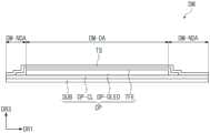
如图2中所示,显示模块DM可以包括显示面板DP和触摸感测单元TS(或触摸感测层)。尽管未被示出,但是显示模块DM还可以包括设置在显示面板DP的底表面上的保护构件以及设置在触摸感测单元TS的顶表面上的抗反射构件和/或窗构件。As shown in FIG. 2 , the display module DM may include a display panel DP and a touch sensing unit TS (or a touch sensing layer). Although not shown, the display module DM may further include a protective member disposed on the bottom surface of the display panel DP and an anti-reflection member and/or a window member disposed on the top surface of the touch sensing unit TS.
显示面板DP可以是发光型显示面板,但发明构思不限于这样的示例。例如,显示面板DP可以是有机发光显示面板或量子点发光显示面板。对于有机发光显示面板,发光层可以包括有机发光材料。对于量子点发光显示面板,发光层可以包括量子点和量子棒。为了简单起见,下面的描述将参考其中显示面板DP是有机发光显示面板的示例。The display panel DP may be a light emitting type display panel, but the inventive concept is not limited to such an example. For example, the display panel DP may be an organic light emitting display panel or a quantum dot light emitting display panel. For an organic light emitting display panel, the light emitting layer may include an organic light emitting material. For a quantum dot light-emitting display panel, the light-emitting layer may include quantum dots and quantum rods. For simplicity, the following description will refer to an example in which the display panel DP is an organic light emitting display panel.
显示面板DP可以包括基体层SUB以及设置在基体层SUB上的电路器件层DP-CL、显示元件层DP-OLED和薄封装层TFE。尽管未被示出,但是显示面板DP还可以包括诸如抗反射层和折射率控制层的功能层。The display panel DP may include a base layer SUB and a circuit device layer DP-CL, a display element layer DP-OLED and a thin encapsulation layer TFE disposed on the base layer SUB. Although not shown, the display panel DP may further include functional layers such as an anti-reflection layer and a refractive index control layer.
基体层SUB可以包括至少一个塑料膜。基体层SUB可以是柔性基底,并且可以包括塑料基底、玻璃基底、金属基底和由有机/无机复合材料制成的基底中的至少一者。参照图1描述的显示区域DM-DA和非显示区域DM-NDA可以以相同的方式被限定在基体层SUB中。The base layer SUB may comprise at least one plastic film. The base layer SUB may be a flexible substrate, and may include at least one of a plastic substrate, a glass substrate, a metal substrate, and a substrate made of an organic/inorganic composite material. The display area DM-DA and the non-display area DM-NDA described with reference to FIG. 1 may be defined in the base layer SUB in the same manner.
电路器件层DP-CL可以包括电路器件和至少一个中间绝缘层。中间绝缘层可以包括至少一个中间无机层和至少一个中间有机层。电路器件可以包括信号线、像素驱动电路等。这将在下面更详细地被描述。The circuit device layer DP-CL may include circuit devices and at least one intermediate insulating layer. The intermediate insulating layer may include at least one intermediate inorganic layer and at least one intermediate organic layer. The circuit devices may include signal lines, pixel driving circuits, and the like. This will be described in more detail below.
显示元件层DP-OLED可以至少包括有机发光二极管。显示元件层DP-OLED还可以包括诸如像素限定层的有机层。The display element layer DP-OLED may include at least an organic light emitting diode. The display element layer DP-OLED may further include an organic layer such as a pixel defining layer.
薄封装层TFE可以对显示元件层DP-OLED进行密封或封装。薄封装层TFE可以包括至少一个无机层(在下文中,无机封装层)。薄封装层TFE还可以包括至少一个有机层(在下文中,有机封装层)。无机封装层可以保护显示元件层DP-OLED不受湿气或氧的影响,并且有机封装层可以保护显示元件层DP-OLED不受诸如灰尘颗粒的污染物质的影响。无机封装层可以由氮化硅、氮氧化硅、氧化硅、氧化钛和氧化铝中的至少一种形成,或者可以包括氮化硅、氮氧化硅、氧化硅、氧化钛和氧化铝中的至少一种。有机封装层可以由丙烯酸类有机材料中的至少一种形成,或者可以包括丙烯酸类有机材料中的至少一种,但发明构思不限于此。The thin encapsulation layer TFE can encapsulate or encapsulate the display element layer DP-OLED. The thin encapsulation layer TFE may include at least one inorganic layer (hereinafter, inorganic encapsulation layer). The thin encapsulation layer TFE may further include at least one organic layer (hereinafter, organic encapsulation layer). The inorganic encapsulation layer may protect the display element layer DP-OLED from moisture or oxygen, and the organic encapsulation layer may protect the display element layer DP-OLED from contaminants such as dust particles. The inorganic encapsulation layer may be formed of at least one of silicon nitride, silicon oxynitride, silicon oxide, titanium oxide, and aluminum oxide, or may include at least one of silicon nitride, silicon oxynitride, silicon oxide, titanium oxide, and aluminum oxide A sort of. The organic encapsulation layer may be formed of at least one of acrylic organic materials, or may include at least one of acrylic organic materials, but the inventive concept is not limited thereto.
触摸感测单元TS可以被构造为获取关于施加到触摸感测单元TS的与显示面板DP的显示区域DP-DA(参见图3)叠置的感测区域的外部输入的坐标的信息。触摸感测单元TS可以直接设置在显示面板DP上。在本说明书中,表述“直接设置”用于表示一个层连续地形成在另一层上,而不形成另外的粘合层。The touch sensing unit TS may be configured to acquire information on coordinates of an external input applied to the sensing area of the touch sensing unit TS overlapping the display area DP-DA (see FIG. 3 ) of the display panel DP. The touch sensing unit TS may be directly disposed on the display panel DP. In this specification, the expression "directly disposed" is used to mean that one layer is continuously formed on another layer without forming an additional adhesive layer.
触摸感测单元TS可以具有多层结构。触摸感测单元TS可以包括一个或更多个导电层。触摸感测单元TS可以包括一个或更多个绝缘层。The touch sensing unit TS may have a multi-layer structure. The touch sensing unit TS may include one or more conductive layers. The touch sensing unit TS may include one or more insulating layers.
触摸感测单元TS可以以电容感测方式感测外部输入。发明构思不限于触摸感测单元TS的特定感测方法,在示例性实施例中,触摸感测单元TS可以以电磁感应方式或压力感测方式感测外部输入。The touch sensing unit TS may sense an external input in a capacitive sensing manner. The inventive concept is not limited to a specific sensing method of the touch sensing unit TS, and in an exemplary embodiment, the touch sensing unit TS may sense an external input in an electromagnetic induction manner or a pressure sensing manner.
图3是示出根据发明构思的示例性实施例的显示面板DP的平面图。FIG. 3 is a plan view illustrating a display panel DP according to an exemplary embodiment of the inventive concept.
如图3中所示,当在平面图中观看时,显示面板DP可以包括显示区域DP-DA和非显示区域DP-NDA。在本实施例中,可以沿着显示区域DP-DA的边界限定非显示区域DP-NDA。显示面板DP的显示区域DP-DA和非显示区域DP-NDA可以分别与图1中示出的显示模块DM的显示区域DM-DA和非显示区域DM-NDA对应。显示面板DP的显示区域DP-DA和非显示区域DP-NDA可以不与显示模块DM的显示区域DM-DA和非显示区域DM-NDA相同,并且可以根据显示面板DP的结构或设计而改变。As shown in FIG. 3 , when viewed in a plan view, the display panel DP may include a display area DP-DA and a non-display area DP-NDA. In this embodiment, the non-display area DP-NDA may be defined along the boundary of the display area DP-DA. The display area DP-DA and the non-display area DP-NDA of the display panel DP may respectively correspond to the display area DM-DA and the non-display area DM-NDA of the display module DM shown in FIG. 1 . The display area DP-DA and the non-display area DP-NDA of the display panel DP may not be the same as the display area DM-DA and the non-display area DM-NDA of the display module DM, and may be changed according to the structure or design of the display panel DP.
显示面板DP可以包括扫描驱动电路SDC、多条信号线DL、CSL、SL和PL以及多个像素PX。像素PX可以设置在显示区域DP-DA中。像素PX中的每个可以包括有机发光二极管和连接到有机发光二极管的像素驱动电路。扫描驱动电路SDC、信号线DL、CSL、SL和PL以及像素驱动电路可以被包括在图2的电路器件层DP-CL中。The display panel DP may include a scan driving circuit SDC, a plurality of signal lines DL, CSL, SL, and PL, and a plurality of pixels PX. The pixels PX may be arranged in the display area DP-DA. Each of the pixels PX may include an organic light emitting diode and a pixel driving circuit connected to the organic light emitting diode. The scan driving circuit SDC, the signal lines DL, CSL, SL, and PL, and the pixel driving circuit may be included in the circuit device layer DP-CL of FIG. 2 .
扫描驱动电路SDC可以产生多个扫描信号,并且可以将多个扫描信号顺序地输出到将在下面描述的多条扫描线SL。扫描驱动电路SDC还可以将其他控制信号输出到像素PX的像素驱动电路。The scan driving circuit SDC may generate a plurality of scan signals, and may sequentially output the plurality of scan signals to a plurality of scan lines SL which will be described below. The scan drive circuit SDC may also output other control signals to the pixel drive circuit of the pixel PX.
扫描驱动电路SDC可以包括由与用于像素PX的像素驱动电路的工艺相同的工艺(例如,由低温多晶硅(LTPS)工艺或低温多晶氧化物(LTPO)工艺)形成的多个薄膜晶体管。The scan driving circuit SDC may include a plurality of thin film transistors formed by the same process as that used for the pixel driving circuit of the pixel PX, eg, a low temperature polysilicon (LTPS) process or a low temperature poly oxide (LTPO) process.
扫描线SL中的每条可以连接到多个像素PX中的对应的像素PX,并且数据线DL中的每条可以连接到多个像素PX中的对应的像素PX。电力线PL可以连接到多个像素PX。控制信号线CSL可以将控制信号提供到扫描驱动电路SDC。Each of the scan lines SL may be connected to a corresponding pixel PX of the plurality of pixels PX, and each of the data lines DL may be connected to a corresponding pixel PX of the plurality of pixels PX. The power line PL may be connected to a plurality of pixels PX. The control signal line CSL may supply a control signal to the scan driving circuit SDC.
显示面板DP可以包括分别连接到信号线DL、CSL、SL和PL的端部的信号垫(pad,或称为“焊盘”)DP-PD。在实施例中,信号垫DP-PD中的每个可以是一种电路器件。非显示区域DP-NDA的其上设置有信号垫DP-PD的部分可以被限定为垫区域NDA-PD。连接到将在下面描述的触摸信号线的触摸垫TS-PD可以设置在垫区域NDA-PD上。The display panel DP may include signal pads (or "pads") DP-PD connected to ends of the signal lines DL, CSL, SL, and PL, respectively. In an embodiment, each of the signal pads DP-PD may be a circuit device. A portion of the non-display area DP-NDA on which the signal pads DP-PD are disposed may be defined as a pad area NDA-PD. A touch pad TS-PD connected to a touch signal line to be described below may be disposed on the pad area NDA-PD.
第一电力图案PP1和第二电力图案PP2可以设置在非显示区域DP-NDA中。第一电力图案PP1可以在第二方向轴DR2上延伸。第二电力图案PP2可以具有矩形形状,所述矩形形状具有在第一方向轴DR1上延伸的第一边和在第二方向轴DR2上延伸的第二边。当在平面图中观看时,第一电力图案PP1和第二电力图案PP2可以彼此间隔开。第一电力图案PP1和第二电力图案PP2的形状和布置可以从图5中的形状和布置进行各种改变。The first power pattern PP1 and the second power pattern PP2 may be disposed in the non-display area DP-NDA. The first power pattern PP1 may extend on the second direction axis DR2. The second power pattern PP2 may have a rectangular shape having a first side extending on the first direction axis DR1 and a second side extending on the second direction axis DR2. When viewed in a plan view, the first power pattern PP1 and the second power pattern PP2 may be spaced apart from each other. The shapes and arrangements of the first and second power patterns PP1 and PP2 may be variously changed from those in FIG. 5 .
第一电力图案PP1可以电连接到信号垫DP-PD的第一电力垫PDD,并且第二电力图案PP2可以电连接到信号垫DP-PD的第二电力垫PDS。在这样的实施例中,第一电力图案PP1和第二电力图案PP2中的每个可以连接到单个垫,但发明构思不限于这样的示例。例如,第一电力图案PP1和第二电力图案PP2中的每个可以电连接到两个或更多个垫。The first power pattern PP1 may be electrically connected to the first power pad PDD of the signal pads DP-PD, and the second power pattern PP2 may be electrically connected to the second power pad PDS of the signal pads DP-PD. In such an embodiment, each of the first power pattern PP1 and the second power pattern PP2 may be connected to a single pad, but the inventive concept is not limited to such an example. For example, each of the first power pattern PP1 and the second power pattern PP2 may be electrically connected to two or more pads.
图4是示出根据发明构思的示例性实施例的像素PX的等效电路图。FIG. 4 is an equivalent circuit diagram illustrating a pixel PX according to an exemplary embodiment of the inventive concept.
图4示例性地示出了连接到扫描线SL中的一条、数据线DL中的一条和电力线PL的一个像素PX。像素PX的结构不限于这样的示例并且可以采用其他形式。FIG. 4 exemplarily shows one pixel PX connected to one of the scan lines SL, one of the data lines DL, and the power line PL. The structure of the pixel PX is not limited to such an example and may take other forms.
有机发光二极管OLED可以是顶发射型二极管或底发射型二极管。像素PX可以包括用作用于驱动有机发光二极管OLED的像素驱动电路的第一晶体管或开关晶体管T1、第二晶体管或驱动晶体管T2以及电容器Cst。第一电力电压ELVDD可以提供到第二晶体管T2,并且第二电力电压ELVSS可以提供到有机发光二极管OLED。第二电力电压ELVSS可以比第一电力电压ELVDD低。The organic light emitting diode OLED may be a top-emitting diode or a bottom-emitting diode. The pixel PX may include a first transistor or switching transistor T1, a second transistor or driving transistor T2, and a capacitor Cst serving as a pixel driving circuit for driving the organic light emitting diode OLED. The first power voltage ELVDD may be supplied to the second transistor T2, and the second power voltage ELVSS may be supplied to the organic light emitting diode OLED. The second power voltage ELVSS may be lower than the first power voltage ELVDD.
第一电力电压ELVDD可以通过图3中示出的第一电力垫PDD和第一电力图案PP1来接收。第二电力电压ELVSS可以通过图3中示出的第二电力垫PDS和第二电力图案PP2来接收。The first power voltage ELVDD may be received through the first power pad PDD and the first power pattern PP1 shown in FIG. 3 . The second power voltage ELVSS may be received through the second power pad PDS and the second power pattern PP2 shown in FIG. 3 .
如果扫描信号施加到扫描线SL,那么第一晶体管T1可以响应于扫描信号而输出施加到数据线DL的数据信号。电容器Cst可以被充电以具有与从第一晶体管T1传输的数据信号对应的电压。If the scan signal is applied to the scan line SL, the first transistor T1 may output the data signal applied to the data line DL in response to the scan signal. The capacitor Cst may be charged to have a voltage corresponding to the data signal transmitted from the first transistor T1.
第二晶体管T2可以连接到有机发光二极管OLED。第二晶体管T2可以根据储存在电容器Cst中的电荷的量来控制流过有机发光二极管OLED的驱动电流。当第二晶体管T2处于导通时段时,有机发光二极管OLED可以发光。The second transistor T2 may be connected to the organic light emitting diode OLED. The second transistor T2 may control the driving current flowing through the organic light emitting diode OLED according to the amount of charges stored in the capacitor Cst. When the second transistor T2 is in the turn-on period, the organic light emitting diode OLED may emit light.
图5是示出根据发明构思的示例性实施例的触摸感测单元TS的平面图。FIG. 5 is a plan view illustrating a touch sensing unit TS according to an exemplary embodiment of the inventive concept.
在图5中,示出了设置在显示面板DP中的第一电力图案PP1和第二电力图案PP2以清楚地示出第一电力图案PP1和第二电力图案PP2相对于触摸感测单元TS的位置。在本实施例中,第一触摸信号线SL1-1至SL1-5和第二触摸信号线SL2-1至SL2-4被示出为分别连接到第一触摸电极TE1-1至TE1-5和第二触摸电极TE2-1至TE2-4的端部,但在实施例中,可以设置更多的信号线。例如,还可以设置连接到第二触摸电极TE2-1至TE2-4的相对的端部的第三触摸信号线。连接到第三触摸信号线的触摸垫也可以并排地设置在图5中示出的触摸垫TS-PD旁边。此外,也可以改变第一触摸信号线SL1-1至SL1-5和第二触摸信号线SL2-1至SL2-4的布置。第一触摸电极TE1-1至TE1-5中的每个可以具有其中限定有多个触摸开口的网格形状。第一触摸电极TE1-1至TE1-5中的每个可以包括多个第一触摸传感器单元SP1和多个第一连接部CP1。第一触摸传感器单元SP1可以沿着第二方向轴DR2布置。第一连接部CP1中的每个可以将第一触摸传感器单元SP1中的相邻的两个彼此连接。尽管未被详细地示出,但是第一触摸信号线SL1-1至SL1-5可以具有网格形状。In FIG. 5 , the first power pattern PP1 and the second power pattern PP2 provided in the display panel DP are shown to clearly show the relation of the first power pattern PP1 and the second power pattern PP2 with respect to the touch sensing unit TS Location. In the present embodiment, the first touch signal lines SL1-1 to SL1-5 and the second touch signal lines SL2-1 to SL2-4 are shown as being connected to the first touch electrodes TE1-1 to TE1-5 and Ends of the second touch electrodes TE2-1 to TE2-4, but in an embodiment, more signal lines may be provided. For example, third touch signal lines connected to opposite ends of the second touch electrodes TE2-1 to TE2-4 may also be provided. The touch pads connected to the third touch signal lines may also be arranged side by side beside the touch pads TS-PD shown in FIG. 5 . In addition, the arrangement of the first touch signal lines SL1-1 to SL1-5 and the second touch signal lines SL2-1 to SL2-4 may also be changed. Each of the first touch electrodes TE1-1 to TE1-5 may have a mesh shape in which a plurality of touch openings are defined. Each of the first touch electrodes TE1-1 to TE1-5 may include a plurality of first touch sensor units SP1 and a plurality of first connection parts CP1. The first touch sensor units SP1 may be arranged along the second direction axis DR2. Each of the first connection parts CP1 may connect adjacent two of the first touch sensor units SP1 to each other. Although not shown in detail, the first touch signal lines SL1-1 to SL1-5 may have a mesh shape.
第二触摸电极TE2-1至TE2-4可以以电断开的方式与第一触摸电极TE1-1至TE1-5交叉。第二触摸电极TE2-1至TE2-4中的每个可以具有其中限定有多个触摸开口的网格形状。第二触摸电极TE2-1至TE2-4中的每个可以包括多个第二触摸传感器单元SP2和多个第二连接部CP2。第二触摸传感器单元SP2可以沿着第一方向轴DR1布置。第二连接部CP2中的每个可以将第二触摸传感器单元SP2中的相邻的两个彼此连接。第二触摸信号线SL2-1至SL2-4也可以具有网格形状。The second touch electrodes TE2-1 to TE2-4 may cross the first touch electrodes TE1-1 to TE1-5 in an electrically disconnected manner. Each of the second touch electrodes TE2-1 to TE2-4 may have a mesh shape in which a plurality of touch openings are defined. Each of the second touch electrodes TE2-1 to TE2-4 may include a plurality of second touch sensor units SP2 and a plurality of second connection parts CP2. The second touch sensor unit SP2 may be arranged along the first direction axis DR1. Each of the second connection parts CP2 may connect adjacent two of the second touch sensor units SP2 to each other. The second touch signal lines SL2-1 to SL2-4 may also have a mesh shape.
第一触摸电极TE1-1至TE1-5可以与第二触摸电极TE2-1至TE2-4电容耦合。施加到第一触摸电极TE1-1至TE1-5的触摸感测信号可以改变第一触摸传感器单元SP1与第二触摸传感器单元SP2之间的电容。The first touch electrodes TE1-1 to TE1-5 may be capacitively coupled with the second touch electrodes TE2-1 to TE2-4. The touch sensing signals applied to the first touch electrodes TE1-1 to TE1-5 may change the capacitance between the first touch sensor unit SP1 and the second touch sensor unit SP2.
图5示出了触摸感测单元TS的其中第一连接部CP1和第二连接部CP2设置为彼此交叉的示例,但发明构思不限于这样的示例。例如,为了防止第二连接部CP2与第一连接部CP1叠置,可以将第二连接部CP2中的每个的形状改变为具有V形结构。在实施例中,即使第二连接部CP2具有V形结构,第二连接部CP2也可能会与第一触摸传感器单元SP1叠置。在本实施例中,第一触摸传感器单元SP1和第二触摸传感器单元SP2被示出为具有菱形或三角形形状,但发明构思不限于这些示例。FIG. 5 shows an example of the touch sensing unit TS in which the first connection part CP1 and the second connection part CP2 are arranged to cross each other, but the inventive concept is not limited to such an example. For example, in order to prevent the second connection parts CP2 from overlapping the first connection parts CP1, the shape of each of the second connection parts CP2 may be changed to have a V-shaped structure. In an embodiment, even if the second connection part CP2 has a V-shaped structure, the second connection part CP2 may overlap the first touch sensor unit SP1. In the present embodiment, the first touch sensor unit SP1 and the second touch sensor unit SP2 are shown to have a rhombus or a triangular shape, but the inventive concept is not limited to these examples.
尽管未在图5中被示出,但是触摸感测单元TS可以是包括导电层和触摸绝缘层的单层触摸感测单元。单层触摸感测单元可以以自电容方式获取坐标信息。Although not shown in FIG. 5 , the touch sensing unit TS may be a single-layer touch sensing unit including a conductive layer and a touch insulating layer. The single-layer touch sensing unit can acquire coordinate information in a self-capacitance manner.
图6是示出根据发明构思的示例性实施例的触摸测试装置100的框图。FIG. 6 is a block diagram illustrating a
参照图6,触摸测试装置100可以用于测试图5中示出的触摸感测单元TS的操作。触摸测试装置100可以响应于来自外部主机(例如,计算机系统105)的测试控制信号TEST_CTRL而测试触摸感测单元TS,并且可以将测试反馈信号TEST_FB提供到计算机系统105。Referring to FIG. 6 , the
在发明构思的示例性实施例中,触摸测试装置100可以测量图3中示出的显示面板DP的第一电力垫PDD和第二电力垫PDS之间的电容,并且可以将关于所测量的电容的信息输出为测试反馈信号TEST_FB。In an exemplary embodiment of the inventive concept, the
连接件110可以电连接到图3中示出的触摸垫TS-PD和信号垫DP-PD中的一些(例如,第一电力垫PDD和第二电力垫PDS)。The
触摸测试装置100可以包括连接件110、触摸测试电路120和接口130。接口130可以响应于来自计算机系统105的测试控制信号TEST_CTRL而将用于测试显示面板DP的电压控制信号CTRL_V提供到触摸测试电路120。The
触摸测试电路120可以响应于电压控制信号CTRL_V而通过连接件110感测显示面板DP的电容,并且可以将与所感测的电容对应的电容感测信号S_CAP输出到接口130。接口130可以将用作测试反馈信号TEST_FB的电容感测信号S_CAP提供到计算机系统105。The
在示例性实施例中,触摸测试电路120可以以单个集成单路的形式来实现。In an exemplary embodiment, the
在示例性实施例中,连接件110可以设置在用于测试图1的显示模块DM的引脚板上。在实施例中,连接件110可以包括位于柔性印刷电路板(FPCB)上的垫,并且触摸测试电路120可以安装在FPCB上。如上所述,连接件110可以用于将图1中示出的显示模块DM连接到触摸测试电路120,但发明构思不限于这样的连接结构。可以各种地改变用于(例如,使用连接件110)将显示模块DM连接到触摸测试电路120的结构。In an exemplary embodiment, the
图7是示出图3中示出的显示面板DP与图6中示出的触摸测试装置100之间的示例连接结构的框图。FIG. 7 is a block diagram showing an example connection structure between the display panel DP shown in FIG. 3 and the
参照图7,连接件110可以包括连接到显示面板DP的触摸垫TS-PD的触摸测试垫TPD以及分别电连接到显示面板DP的第一电力垫PDD和第二电力垫PDS的第一电力测试垫TDD和第二电力测试垫TDS。7 , the
触摸测试电路120可以包括触摸测试器210、电容测量电路220和电压产生器230。触摸测试器210可以产生用于测试图5中示出的触摸感测单元TS的触摸测试信号TTS。触摸测试信号TTS可以通过触摸测试垫TPD提供到显示面板DP的触摸垫TS-PD。由于触摸垫TS-PD连接到图5的第一触摸信号线SL1-1至SL1-5和第二触摸信号线SL2-1至SL2-4,所以可以利用触摸测试信号TTS测试触摸感测单元TS。The
电压产生器230可以产生第一电力电压ELVDD和第二电力电压ELVSS。在这样的实施例中,电压产生器230被描述为仅产生两种电压ELVDD和ELVSS,但发明构思不限于这样的示例。例如,电压产生器230可以产生测试图5的触摸感测单元TS所需的各种电压。电压产生器230可以响应于电压控制信号CTRL_V而控制第一电力电压ELVDD和第二电力电压ELVSS中的每个的电压电平。The
由电压产生器230产生的第一电力电压ELVDD和第二电力电压ELVSS可以通过第一电力测试垫TDD和第二电力测试垫TDS分别提供到第一电力垫PDD和第二电力垫PDS。当触摸测试器210输出触摸测试信号TTS时,电压产生器230输出第一电力电压ELVDD和第二电力电压ELVSS。与此同时,第一电力电压ELVDD和第二电力电压ELVSS可以分别与第一测试电力电压和第二测试电力电压对应。The first power voltage ELVDD and the second power voltage ELVSS generated by the
电容测量电路220可以测量第一电力测试垫TDD与第二电力测试垫TDS之间的电容。电容测量电路220可以输出与所测量的电容对应的电容感测信号S_CAP。The
在示例性实施例中,电容测量电路220可以用于测量第一电力测试垫TDD与第二电力测试垫TDS之间的电容,但发明构思不限于这样的示例。电容测量电路220可以是设置为测试触摸感测单元TS的特性的器件。在这种情况下,由于利用设置为测试触摸感测单元TS的特性的电容测量电路220来测量显示面板DP的电容,所以不必提供用于测量显示面板DP的电容的专用电容测量电路。In an exemplary embodiment, the
参照图4和图7,第一电力电压ELVDD可以通过电力线PL传输至第二晶体管T2,并且第二电力电压ELVSS可以传输至有机发光二极管OLED的阴极端子。4 and 7 , the first power voltage ELVDD may be transmitted to the second transistor T2 through the power line PL, and the second power voltage ELVSS may be transmitted to the cathode terminal of the organic light emitting diode OLED.
可以测量有机发光二极管OLED的阳极端子和阴极端子之间的静电电容以检查有机发光二极管OLED是否劣化。有机发光二极管OLED的阳极端子可以通过第二晶体管T2供应有第一电力电压ELVDD,并且有机发光二极管OLED的阴极端子可以供应有第二电力电压ELVSS。通过利用第一电力电压ELVDD和第二电力电压ELVSS来测量第一电力垫PDD与第二电力垫PDS之间的电容,可以能够确定有机发光二极管OLED是否劣化。The electrostatic capacitance between the anode terminal and the cathode terminal of the organic light emitting diode OLED may be measured to check whether the organic light emitting diode OLED is deteriorated. The anode terminal of the organic light emitting diode OLED may be supplied with the first power voltage ELVDD through the second transistor T2, and the cathode terminal of the organic light emitting diode OLED may be supplied with the second power voltage ELVSS. By measuring the capacitance between the first power pad PDD and the second power pad PDS using the first power voltage ELVDD and the second power voltage ELVSS, it may be possible to determine whether the organic light emitting diode OLED is degraded.
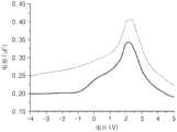
图8A、图8B和图8C是均示出由图7中示出的第一电力垫PDD与第二电力垫PDS之间的电压差导致的电容的变化的曲线图。在图8A至图8C中,实线表示正常状态下的电容,并且虚线表示非正常状态下的电容。FIGS. 8A , 8B, and 8C are graphs each showing a change in capacitance caused by a voltage difference between the first power pad PDD and the second power pad PDS shown in FIG. 7 . In FIGS. 8A to 8C , the solid line represents the capacitance in the normal state, and the broken line represents the capacitance in the abnormal state.
图8A示出了蓝色有机发光二极管的电容特性,图8B示出了绿色有机发光二极管的电容特性,并且图8C示出了红色有机发光二极管的电容特性。FIG. 8A shows the capacitance characteristic of the blue organic light emitting diode, FIG. 8B shows the capacitance characteristic of the green organic light emitting diode, and FIG. 8C shows the capacitance characteristic of the red organic light emitting diode.
如图8A至图8C中所示,有机发光二极管的电容特性可以根据分别提供到第一电力测试垫TDD和第二电力测试垫TDS的第一电力电压ELVDD与第二电力电压ELVSS之间的差而变化。As shown in FIGS. 8A to 8C , the capacitance characteristics of the organic light emitting diode may be based on the difference between the first power voltage ELVDD and the second power voltage ELVSS supplied to the first power test pad TDD and the second power test pad TDS, respectively and change.
此外,有机发光二极管的电容特性可以根据有机发光二极管是处于正常状态还是处于非正常(例如,劣化)状态而变化。如图8A至图8C中所示,蓝色有机发光二极管、绿色有机发光二极管和红色有机发光二极管中的全部在非正常状态下具有比在正常状态下高的电容。Also, the capacitance characteristics of the organic light emitting diode may vary according to whether the organic light emitting diode is in a normal state or an abnormal (eg, degraded) state. As shown in FIGS. 8A to 8C , all of the blue organic light emitting diodes, the green organic light emitting diodes, and the red organic light emitting diodes have higher capacitances in the abnormal state than in the normal state.
图7中示出的电压产生器230可以响应于电压控制信号CTRL_V而控制第一电力电压ELVDD和第二电力电压ELVSS中的每个的电压电平。例如,电压产生器230可以固定第一电力电压ELVDD和第二电力电压ELVSS中的一个的电压电平并且可以改变第一电力电压ELVDD和第二电力电压ELVSS中的另一个的电压电平。在实施例中,电压产生器230可以同时改变第一电力电压ELVDD和第二电力电压ELVSS。例如,如图8A至图8C中所示,可以将第一电力电压ELVDD和第二电力电压ELVSS改变为具有在-5V至6V的范围内的电压差。The
电容测量电路220可以测量第一电力测试垫TDD与第二电力测试垫TDS之间的电容。电容测量电路220可以输出与所测量的电容对应的电容感测信号S_CAP。The
可以通过利用为触摸感测单元TS准备的电容测量电路220来测试显示面板DP的有机发光二极管OLED的电容。因此,不必提供仅用于测量显示面板DP的电容的另外的电容测量电路。The capacitance of the organic light emitting diode OLED of the display panel DP may be tested by using the
图9是示出根据发明构思的另一示例性实施例的触摸测试装置300的框图。图10是示出图9的触摸测试电路320的结构的示例的图。FIG. 9 is a block diagram illustrating a
如图9中所示,触摸测试装置300可以响应于来自外部主机(例如,计算机系统305)的测试控制信号TEST_CTRL而测试触摸感测单元TS,并且可以将测试反馈信号TEST_FB提供到计算机系统305。触摸测试装置300可以包括连接件310、触摸测试电路320、测试信号产生电路330和接口340。在图9中示出的实施例中,触摸测试电路320和接口340可以与参照图6描述的触摸测试电路120和接口130具有相同的电路结构和操作。As shown in FIG. 9 , the
参照图9和图10,连接件310可以包括可分别电连接到图3中示出的触摸垫TS-PD和信号垫DP-PD的触摸测试垫TPD和显示面板测试垫DPD。显示面板测试垫DPD可以包括第一电力测试垫TDD和第二电力测试垫TDS。Referring to FIGS. 9 and 10 , the
电压产生器430可以响应于电压控制信号CTRL_V而产生第一电力电压ELVDD和第二电力电压ELVSS。第一电力电压ELVDD和第二电力电压ELVSS可以分别提供到第一电力测试垫TDD和第二电力测试垫TDS。The
触摸测试器410可以产生用于测试图5中示出的触摸感测单元TS的触摸测试信号TTS。电容测量电路420可以测量第一电力测试垫TDD与第二电力测试垫TDS之间的电容。电容测量电路420可以输出与所测量的电容对应的电容感测信号S_CAP。The
测试信号产生电路330和显示面板测试垫DPD一起可以被称为面板测试电路。测试信号产生电路330可以响应于来自接口340的测试信号TSIG而产生将提供到显示面板测试垫DPD的测试信号(或称为面板测试信号)。例如,测试信号可以包括将提供到图3中示出的显示面板DP的扫描驱动电路SDC的时钟信号和将提供到数据线DL的数据信号。The test
触摸测试装置300的测试信号产生电路330可以将时钟信号和数据信号提供到显示面板DP,并且电压产生器430可以将第一电力电压ELVDD和第二电力电压ELVSS提供到显示面板DP。The test
因此,当响应于第一电力电压ELVDD、第二电力电压ELVSS、时钟信号和数据信号而执行显示面板DP的操作时,电容测量电路420可以测量第一电力测试垫TDD与第二电力测试垫TDS之间的电容。Therefore, when the operation of the display panel DP is performed in response to the first power voltage ELVDD, the second power voltage ELVSS, the clock signal and the data signal, the
图11是示出根据发明构思的另一示例性实施例的显示模块DM2的透视图。FIG. 11 is a perspective view illustrating a display module DM2 according to another exemplary embodiment of the inventive concept.
参照图11,显示模块DM2可以包括显示面板DP2、触摸感测单元TS2(或触摸感测层)、第一电路基底CF1、第二电路基底CF2和连接件CNT。11 , the display module DM2 may include a display panel DP2, a touch sensing unit TS2 (or a touch sensing layer), a first circuit substrate CF1, a second circuit substrate CF2, and a connection member CNT.
第一电路基底CF1可以电连接到显示面板DP2。第一电路基底CF1可以将显示面板DP2连接到连接件CNT。在本实施例中,第一电路基底CF1可以是柔性电路膜。然而,发明构思不限于这样的示例,在实施例中,第一电路基底CF1可以是刚性基底。The first circuit substrate CF1 may be electrically connected to the display panel DP2. The first circuit substrate CF1 may connect the display panel DP2 to the connector CNT. In this embodiment, the first circuit substrate CF1 may be a flexible circuit film. However, the inventive concept is not limited to such an example, and in an embodiment, the first circuit substrate CF1 may be a rigid substrate.
第二电路基底CF2可以电连接到触摸感测单元TS2。第二电路基底CF2可以将触摸感测单元TS2连接到连接件CNT。在本实施例中,第二电路基底CF2可以是柔性电路膜,但发明构思不限于这样的示例。例如,第二电路基底CF2可以是刚性基底。The second circuit substrate CF2 may be electrically connected to the touch sensing unit TS2. The second circuit substrate CF2 may connect the touch sensing unit TS2 to the connector CNT. In this embodiment, the second circuit substrate CF2 may be a flexible circuit film, but the inventive concept is not limited to such an example. For example, the second circuit substrate CF2 may be a rigid substrate.
图12是示出图11中示出的显示面板DP2与图6中示出的触摸测试装置100之间的示例连接结构的图。FIG. 12 is a diagram showing an example connection structure between the display panel DP2 shown in FIG. 11 and the
在图12中示出的显示面板DP2和触摸测试电路120中,之前参照图3或图7描述的元件可以通过相同的附图标记来标识而不重复它们的重复描述。In the display panel DP2 and the
图7的显示面板DP可以包括其上设置有信号垫DP-PD以及触摸垫TS-PD的垫区域NDA-PD。相比之下,仅信号垫DP-PD可以设置在图12的显示模块DM2的垫区域NDA-PD2上。The display panel DP of FIG. 7 may include a pad area NDA-PD on which the signal pads DP-PD and the touch pads TS-PD are disposed. In contrast, only the signal pads DP-PD may be disposed on the pad area NDA-PD2 of the display module DM2 of FIG. 12 .
连接件CNT可以包括分别电连接到显示面板DP2的第一电力垫PDD和第二电力垫PDS的第一电力测试垫TDD和第二电力测试垫TDS。连接件CNT还可以包括可电连接到图11中示出的触摸感测单元TS2的触摸测试垫TPD。The connector CNT may include a first power test pad TDD and a second power test pad TDS electrically connected to the first power pad PDD and the second power pad PDS of the display panel DP2, respectively. The connector CNT may further include a touch test pad TPD electrically connectable to the touch sensing unit TS2 shown in FIG. 11 .
如上所述,连接件CNT可以用于将图11的显示面板DP2和触摸感测单元TS2连接到触摸测试电路120,但发明构思不限于这样的连接结构。可以各种地改变用于(例如,利用连接件CNT)将图11的显示面板DP2和触摸感测单元TS2连接到触摸测试电路120的结构。As described above, the connector CNT may be used to connect the display panel DP2 and the touch sensing unit TS2 of FIG. 11 to the
触摸测试电路120可以响应于电压控制信号CTRL_V而通过连接件CNT感测显示面板DP2的电容,并且可以输出与所感测的电容对应的电容感测信号S_CAP。The
如图11和图12中所示,即使显示面板DP2的信号垫DP-PD布置在与用于触摸感测单元TS2的触摸垫(未示出)的层不同的层上,也可以利用触摸测试装置100来测量或测试显示面板DP2的有机发光二极管的电容。因此,不必提供用于仅测量显示面板DP2的电容的另外的电容测量电路。As shown in FIGS. 11 and 12 , even if the signal pads DP-PD of the display panel DP2 are arranged on a layer different from that used for the touch pads (not shown) of the touch sensing unit TS2 , the touch test can be utilized The
根据发明构思的示例性实施例,测试装置可以用于在测试显示模块的触摸感测单元的步骤中测量显示面板的电容。因此,不必提供用于测量显示面板的电容的另外的测试装置。According to an exemplary embodiment of the inventive concept, a testing apparatus may be used to measure the capacitance of the display panel in the step of testing the touch sensing unit of the display module. Therefore, it is not necessary to provide an additional test device for measuring the capacitance of the display panel.
尽管在这里已经描述了某些示例性实施例和实施方式,但是其他的实施例和修改通过该描述将是明显的。因此,发明构思不限于这样的实施例,而是限于所附权利要求以及如对本领域普通技术人员而言将明显的各种明显的修改和等同布置的更宽范围。While certain exemplary embodiments and implementations have been described herein, other embodiments and modifications will be apparent from this description. Therefore, the inventive concepts are not limited to such embodiments, but rather to the appended claims and their broader scope with various obvious modifications and equivalent arrangements as will be apparent to those skilled in the art.
Claims (10)
Applications Claiming Priority (2)
| Application Number | Priority Date | Filing Date | Title |
|---|---|---|---|
| KR1020180161103AKR102581763B1 (en) | 2018-12-13 | 2018-12-13 | Testing device of display module, testing system having the same and testing method of the same |
| KR10-2018-0161103 | 2018-12-13 |
Publications (2)
| Publication Number | Publication Date |
|---|---|
| CN111326089Atrue CN111326089A (en) | 2020-06-23 |
| CN111326089B CN111326089B (en) | 2024-07-26 |
Family
ID=71071562
Family Applications (1)
| Application Number | Title | Priority Date | Filing Date |
|---|---|---|---|
| CN201911264355.0AActiveCN111326089B (en) | 2018-12-13 | 2019-12-11 | Test device and test system |
Country Status (3)
| Country | Link |
|---|---|
| US (1) | US11409395B2 (en) |
| KR (1) | KR102581763B1 (en) |
| CN (1) | CN111326089B (en) |
Families Citing this family (5)
| Publication number | Priority date | Publication date | Assignee | Title |
|---|---|---|---|---|
| WO2020246300A1 (en)* | 2019-06-04 | 2020-12-10 | 株式会社クオルテック | Semiconductor element testing device and testing method for semiconductor element |
| KR20210085999A (en)* | 2019-12-31 | 2021-07-08 | 엘지디스플레이 주식회사 | Display Panel And Large Display Apparatus Having The Same |
| US11957013B2 (en)* | 2020-03-27 | 2024-04-09 | Boe Technology Group Co., Ltd. | Display panel and display device for IVL testing |
| KR20220044044A (en)* | 2020-09-29 | 2022-04-06 | 삼성디스플레이 주식회사 | Display device |
| KR20230020048A (en)* | 2021-08-02 | 2023-02-10 | 삼성디스플레이 주식회사 | Touch testing apparatus of touch detection module and method for testing the same |
Citations (8)
| Publication number | Priority date | Publication date | Assignee | Title |
|---|---|---|---|---|
| US20130271677A1 (en)* | 2012-04-12 | 2013-10-17 | Samsung Display Co., Ltd. | Display apparatus and method of measuring liquid crystal capacitance |
| CN103513816A (en)* | 2012-06-14 | 2014-01-15 | 三星显示有限公司 | Display device |
| CN104217672A (en)* | 2013-05-31 | 2014-12-17 | 三星显示有限公司 | Organic light emitting display panel |
| CN105511136A (en)* | 2014-10-14 | 2016-04-20 | 乐金显示有限公司 | Liquid crystal display device with touch screen and test method for touch panel |
| CN106206654A (en)* | 2015-05-26 | 2016-12-07 | 三星显示有限公司 | Display device |
| CN107092388A (en)* | 2017-04-12 | 2017-08-25 | 北京集创北方科技股份有限公司 | Touch control display apparatus and its driving method |
| US20180122863A1 (en)* | 2016-11-02 | 2018-05-03 | Samsung Display Co., Ltd. | Display device |
| CN108874194A (en)* | 2017-05-10 | 2018-11-23 | 南京瀚宇彩欣科技有限责任公司 | Embedded touch display device, testing method and manufacturing method thereof |
Family Cites Families (9)
| Publication number | Priority date | Publication date | Assignee | Title |
|---|---|---|---|---|
| JPH0627494A (en) | 1992-02-14 | 1994-02-04 | Inter Tec:Kk | Inspecting method and device for thin-film transistor active matrix substrate |
| KR20040072285A (en) | 2003-02-10 | 2004-08-18 | 삼성전자주식회사 | Apparatus for testing flexible printed circuit board |
| KR102034069B1 (en) | 2012-10-30 | 2019-10-21 | 엘지디스플레이 주식회사 | Touch mode liquid crystal display device and inspecting method thereof |
| KR102090715B1 (en)* | 2013-08-02 | 2020-03-19 | 삼성디스플레이 주식회사 | Method and apparatus for measuring capacitance of organic light emitting device |
| KR102581855B1 (en) | 2016-12-22 | 2023-09-21 | 엘지디스플레이 주식회사 | Display device and method for driving the same |
| KR102552144B1 (en) | 2016-12-22 | 2023-07-05 | 엘지디스플레이 주식회사 | Touch Device And Method Of Inspecting And Calibrating The Same |
| KR102668622B1 (en)* | 2016-12-29 | 2024-05-24 | 삼성디스플레이 주식회사 | Display device and manufacturing method of the same |
| KR102426008B1 (en)* | 2017-05-15 | 2022-07-29 | 삼성디스플레이 주식회사 | Input sensing circuit and display module having the same |
| KR102520563B1 (en)* | 2018-11-07 | 2023-04-10 | 엘지디스플레이 주식회사 | Driving voltage sensing circuit and display device using it |
- 2018
- 2018-12-13KRKR1020180161103Apatent/KR102581763B1/enactiveActive
- 2019
- 2019-10-29USUS16/667,335patent/US11409395B2/enactiveActive
- 2019-12-11CNCN201911264355.0Apatent/CN111326089B/enactiveActive
Patent Citations (8)
| Publication number | Priority date | Publication date | Assignee | Title |
|---|---|---|---|---|
| US20130271677A1 (en)* | 2012-04-12 | 2013-10-17 | Samsung Display Co., Ltd. | Display apparatus and method of measuring liquid crystal capacitance |
| CN103513816A (en)* | 2012-06-14 | 2014-01-15 | 三星显示有限公司 | Display device |
| CN104217672A (en)* | 2013-05-31 | 2014-12-17 | 三星显示有限公司 | Organic light emitting display panel |
| CN105511136A (en)* | 2014-10-14 | 2016-04-20 | 乐金显示有限公司 | Liquid crystal display device with touch screen and test method for touch panel |
| CN106206654A (en)* | 2015-05-26 | 2016-12-07 | 三星显示有限公司 | Display device |
| US20180122863A1 (en)* | 2016-11-02 | 2018-05-03 | Samsung Display Co., Ltd. | Display device |
| CN107092388A (en)* | 2017-04-12 | 2017-08-25 | 北京集创北方科技股份有限公司 | Touch control display apparatus and its driving method |
| CN108874194A (en)* | 2017-05-10 | 2018-11-23 | 南京瀚宇彩欣科技有限责任公司 | Embedded touch display device, testing method and manufacturing method thereof |
Also Published As
| Publication number | Publication date |
|---|---|
| KR20200073342A (en) | 2020-06-24 |
| US11409395B2 (en) | 2022-08-09 |
| US20200192524A1 (en) | 2020-06-18 |
| CN111326089B (en) | 2024-07-26 |
| KR102581763B1 (en) | 2023-09-25 |
Similar Documents
| Publication | Publication Date | Title |
|---|---|---|
| CN111326089B (en) | Test device and test system | |
| CN110738928B (en) | display device | |
| US11455066B2 (en) | Touch sensor and display device having the same | |
| CN109407906B (en) | Display device | |
| KR102849526B1 (en) | Display device and method for driving the same | |
| CN111628100A (en) | display screen | |
| CN114518808A (en) | touch sensing unit | |
| US11928299B2 (en) | Touch sensor and display device having the same | |
| CN117524020A (en) | Display device | |
| US11102893B2 (en) | Display device | |
| EP4152126A1 (en) | Smart pen and a display device using the same | |
| US10877601B2 (en) | Display device | |
| US20230136335A1 (en) | Input sensing circuit and display module having the same | |
| US20250157247A1 (en) | Fingerprint sensor and display device including the same | |
| US20250046114A1 (en) | Fingerprint sensor and display device including the same | |
| US20250294965A1 (en) | Display device | |
| US20250148979A1 (en) | Display device | |
| US20250169342A1 (en) | Display device and mobile electronic device including same | |
| CN119723626A (en) | Fingerprint sensor and display device including the same |
Legal Events
| Date | Code | Title | Description |
|---|---|---|---|
| PB01 | Publication | ||
| PB01 | Publication | ||
| SE01 | Entry into force of request for substantive examination | ||
| SE01 | Entry into force of request for substantive examination | ||
| GR01 | Patent grant | ||
| GR01 | Patent grant |