Movatterモバイル変換


[0]ホーム

URL:


CN111324552A - Memory system and operating method thereof - Google Patents

Memory system and operating method thereof
Download PDF

Info

Publication number
CN111324552A
CN111324552ACN201911213480.9ACN201911213480ACN111324552ACN 111324552 ACN111324552 ACN 111324552ACN 201911213480 ACN201911213480 ACN 201911213480ACN 111324552 ACN111324552 ACN 111324552A
Authority
CN
China
Prior art keywords
mapped
memory
mapping information
mapping
unmap
Prior art date
Legal status (The legal status is an assumption and is not a legal conclusion. Google has not performed a legal analysis and makes no representation as to the accuracy of the status listed.)
Granted
Application number
CN201911213480.9A
Other languages
Chinese (zh)
Other versions
CN111324552B (en
Inventor
赵荣翼
朴炳奎
Current Assignee (The listed assignees may be inaccurate. Google has not performed a legal analysis and makes no representation or warranty as to the accuracy of the list.)
SK Hynix Inc
Original Assignee
SK Hynix Inc
Priority date (The priority date is an assumption and is not a legal conclusion. Google has not performed a legal analysis and makes no representation as to the accuracy of the date listed.)
Filing date
Publication date
Application filed by SK Hynix IncfiledCriticalSK Hynix Inc
Publication of CN111324552ApublicationCriticalpatent/CN111324552A/en
Application grantedgrantedCritical
Publication of CN111324552BpublicationCriticalpatent/CN111324552B/en
Activelegal-statusCriticalCurrent
Anticipated expirationlegal-statusCritical

Links

Images

Classifications

Landscapes

Abstract

Translated fromChinese

本文描述了存储器系统及其操作方法。一种存储器系统包括:存储器装置,用于存储与针对取消映射命令的目标逻辑地址相关联的第一映射信息和第二映射信息;以及控制器,用于从存储器装置加载第一映射信息和第二映射信息,将与目标逻辑地址相对应的目标映射数据的大小与阈值进行比较,基于比较的结果将与包括目标逻辑地址的多个目标逻辑组分别映射的多个映射段分类到多个区域,并且对区域中包括的映射段中的每一个执行取消映射操作,其中第一映射信息包括关于多个映射段与多个目标逻辑组之间的映射关系的信息,并且第二映射信息包括关于目标逻辑地址与对应的物理地址之间的映射关系的信息。

Figure 201911213480

This document describes a memory system and its method of operation. A memory system includes: a memory device for storing first and second mapping information associated with a target logical address for an unmap command; and a controller for loading the first and second mapping information from the memory device Two mapping information, compare the size of the target mapping data corresponding to the target logical address with the threshold value, and classify the multiple mapping segments respectively mapped with multiple target logical groups including the target logical address into multiple regions based on the result of the comparison , and perform an unmap operation on each of the mapping segments included in the area, wherein the first mapping information includes information about the mapping relationship between the multiple mapping segments and the multiple target logical groups, and the second mapping information includes information about the mapping relationship between the multiple mapping segments and the multiple target logical groups. Information about the mapping relationship between the target logical address and the corresponding physical address.

Figure 201911213480

Description

Translated fromChinese
存储器系统及其操作方法Memory system and method of operation

相关申请的交叉引用CROSS-REFERENCE TO RELATED APPLICATIONS

本申请要求于2018年12月17日提交的韩国专利申请号10-2018-0163281的优先权,其全部内容通过引用并入本文。This application claims priority from Korean Patent Application No. 10-2018-0163281 filed on December 17, 2018, the entire contents of which are incorporated herein by reference.

技术领域technical field

各种实施例涉及存储器系统,并且更具体地涉及能够有效地处理取消映射命令的存储器系统以及存储器系统的操作方法。Various embodiments relate to memory systems, and more particularly, to memory systems and methods of operating memory systems capable of efficiently processing unmap commands.

背景技术Background technique

计算机环境范例已过渡到普适计算,这使得能够随时随地使用计算系统。结果,诸如移动电话、数码相机和膝上型计算机的便携式电子装置的使用迅速增加。这些便携式电子装置通常使用具有一个或多个存储器装置的存储器系统以用于存储数据。存储器系统可以用作便携式电子装置的主存储器装置或辅助存储器装置。The computing environment paradigm has transitioned to ubiquitous computing, which enables computing systems to be used anytime, anywhere. As a result, the use of portable electronic devices such as mobile phones, digital cameras, and laptop computers has rapidly increased. These portable electronic devices typically use memory systems with one or more memory devices for storing data. The memory system can be used as a main memory device or a secondary memory device for the portable electronic device.

由于它们不具有移动部件,存储器系统提供诸如出色的稳定性和耐用性、高信息访问速度以及低功耗等优点。具有这种优点的存储器系统的示例包括通用串行总线(USB)存储器装置、具有各种接口的存储器卡以及固态驱动器(SSD)。Because they have no moving parts, memory systems offer advantages such as excellent stability and durability, high information access speed, and low power consumption. Examples of memory systems with this advantage include Universal Serial Bus (USB) memory devices, memory cards with various interfaces, and solid state drives (SSDs).

发明内容SUMMARY OF THE INVENTION

本发明的各种实施例针对可以有效地处理从主机提供的取消映射命令的存储器系统。Various embodiments of the present invention are directed to memory systems that can efficiently process unmap commands provided from the host.

根据一个实施例,一种存储器系统包括:存储器装置,适于存储与针对取消映射命令的目标逻辑地址相关联的第一映射信息和第二映射信息;以及控制器,适于从存储器装置加载第一映射信息和第二映射信息,将与目标逻辑地址相对应的目标映射数据的大小与阈值进行比较,基于比较的结果来将与包括目标逻辑地址中的一个或多个的多个目标逻辑组分别映射的多个映射段分类到多个区域,并且对多个区域中包括的映射段中的每一个执行取消映射操作,其中第一映射信息包括关于多个映射段与多个目标逻辑组之间的映射关系的信息,并且第二映射信息包括关于目标逻辑地址与对应的物理地址之间的映射关系的信息。According to one embodiment, a memory system includes: a memory device adapted to store first mapping information and second mapping information associated with a target logical address for an unmap command; and a controller adapted to load a first mapping information from the memory device a mapping information and a second mapping information, comparing the size of the target mapping data corresponding to the target logical address with a threshold value, and based on the result of the comparison, matching with a plurality of target logical groups including one or more of the target logical addresses A plurality of mapped segments that are respectively mapped are classified into a plurality of regions, and an unmap operation is performed on each of the mapped segments included in the plurality of regions, wherein the first mapping information includes information about the relationship between the plurality of mapped segments and the plurality of target logical groups. and the second mapping information includes information about the mapping relationship between the target logical address and the corresponding physical address.

根据一个实施例,一种存储器系统的操作方法,该操作方法包括:接收取消映射命令;从存储器装置加载与对应于取消映射命令的目标逻辑地址相关联的第一映射信息和第二映射信息,并且将第一映射信息和第二映射信息存储在存储器中;将对应于目标逻辑地址的目标映射数据的大小与阈值进行比较;基于比较的结果,将与包括一个或多个目标逻辑地址的多个目标逻辑组分别映射的多个映射段分类到多个区域;以及对多个区域中的任一个中包括的每个映射段执行取消映射操作,其中第一映射信息包括关于多个映射段与多个目标逻辑组之间的映射关系的信息,并且第二映射信息包括关于目标逻辑地址与对应物理地址之间的映射关系的信息。According to one embodiment, a method of operating a memory system comprising: receiving an unmap command; loading from a memory device first mapping information and second mapping information associated with a target logical address corresponding to the unmap command, And store the first mapping information and the second mapping information in the memory; compare the size of the target mapping data corresponding to the target logical address with the threshold; The plurality of mapped segments mapped respectively by the target logical groups are classified into a plurality of regions; and an unmap operation is performed on each mapped segment included in any one of the plurality of regions, wherein the first mapping information includes information about the plurality of mapped segments and Information on the mapping relationship between a plurality of target logical groups, and the second mapping information includes information on the mapping relationship between the target logical addresses and the corresponding physical addresses.

根据一个实施例,一种存储器系统包括:存储器装置,适于存储第一映射信息和第二映射信息,第一映射信息包括关于多个映射段与多个逻辑组之间的映射的信息,每个逻辑组包括一个或多个逻辑地址,并且第二映射信息包括关于多个逻辑地址与多个物理地址之间的映射的信息;以及控制器,包括存储器,适于从存储器装置将与取消映射命令相关联的第一映射信息和第二映射信息加载到存储器中;将包括第一映射段、最后映射段和其余映射段的多个映射段划分到包括第一映射段的第一组、包括其余映射段的第二组和包括最后映射段的第三组;以及将针对第一组和第三组的第二映射信息取消映射,并且将针对第二组的第一映射信息取消映射。According to one embodiment, a memory system includes a memory device adapted to store first mapping information and second mapping information, the first mapping information including information regarding mappings between a plurality of mapped segments and a plurality of logical groups, each the logical groups include one or more logical addresses, and the second mapping information includes information about mappings between the plurality of logical addresses and the plurality of physical addresses; and a controller including a memory adapted to unmap and unmap from the memory device Command the associated first mapping information and second mapping information to load into memory; divide a plurality of mapped segments including the first mapped segment, the last mapped segment and the remaining mapped segments into a first group including the first mapped segment, including the second group of remaining mapped segments and the third group including the last mapped segment; and the second mapping information for the first and third groups is unmapped, and the first mapping information for the second group is unmapped.

附图说明Description of drawings

图1是图示根据本发明的实施例的包括存储器系统的数据处理系统的框图。1 is a block diagram illustrating a data processing system including a memory system according to an embodiment of the present invention.

图2是图示图1的存储器系统中采用的存储器装置的示意图。FIG. 2 is a schematic diagram illustrating a memory device employed in the memory system of FIG. 1 .

图3是图示存储器装置中的存储器块的存储器单元阵列的电路图。3 is a circuit diagram illustrating a memory cell array of a memory block in a memory device.

图4是图示存储器装置的示例性三维结构的框图。4 is a block diagram illustrating an exemplary three-dimensional structure of a memory device.

图5A是图示根据本发明的实施例的第一表的结构的图。FIG. 5A is a diagram illustrating a structure of a first table according to an embodiment of the present invention.

图5B是图示根据本发明的实施例的第二表的结构的图。FIG. 5B is a diagram illustrating a structure of a second table according to an embodiment of the present invention.

图6A至图6E是图示根据本发明的实施例的存储器系统的操作的图。6A to 6E are diagrams illustrating operations of a memory system according to an embodiment of the present invention.

图7是图示根据本发明的实施例的存储器系统的操作过程的流程图。FIG. 7 is a flowchart illustrating an operation process of a memory system according to an embodiment of the present invention.

图8至图16是示意性地图示根据本发明的各个实施例的数据处理系统的应用示例的图。8 to 16 are diagrams schematically illustrating application examples of the data processing system according to various embodiments of the present invention.

具体实施方式Detailed ways

下面参考附图来更详细地描述本发明的各种实施例。以下描述集中于与本发明的特征和方面有关的细节。为了不模糊这样的描述,可以省略公知的技术信息。另外,在整个说明书中,对“一个实施例”、“另一实施例”等的引用不一定仅是一个实施例,并且对任何这样的短语的不同引用不一定是相同的(一个或多个)实施例。Various embodiments of the present invention are described in more detail below with reference to the accompanying drawings. The following description focuses on details related to features and aspects of the invention. In order not to obscure such description, well-known technical information may be omitted. In addition, throughout this specification, references to "one embodiment," "another embodiment," etc. are not necessarily to only one embodiment, and different references to any such phrase are not necessarily the same (one or more ) example.

图1是图示根据本发明的实施例的数据处理系统100的框图。FIG. 1 is a block diagram illustrating adata processing system 100 according to an embodiment of the present invention.

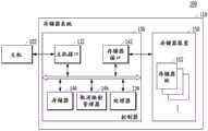
参考图1,数据处理系统100可以包括可操作地耦合到存储器系统110的主机102。Referring to FIG. 1 ,data processing system 100 may includehost 102 operably coupled tomemory system 110 .

主机102可以包括诸如移动电话、MP3播放器和膝上型计算机的各种便携式电子装置中的任一个或者诸如台式计算机、游戏机、电视(TV)以及投影仪的各种非便携式电子装置中的任一个。Host 102 may include any of a variety of portable electronic devices, such as mobile phones, MP3 players, and laptop computers, or a variety of non-portable electronic devices, such as desktop computers, game consoles, televisions (TVs), and projectors. either.

主机102可以包括至少一个操作系统(OS),OS可以管理和控制主机102的整体功能和操作,并且使用数据处理系统100或存储器110来提供主机102和用户之间的操作。OS可以支持与用户的使用目的和使用情况相对应的功能和操作。例如,主机102可以向存储器系统110提供写入命令、读取命令、擦除命令和取消映射命令,并且存储器系统110可以执行与命令相对应的操作。Host 102 may include at least one operating system (OS), which may manage and control the overall functions and operations ofhost 102 and usedata processing system 100 ormemory 110 to provide operations betweenhost 102 and a user. The OS can support functions and operations corresponding to the user's purpose of use and usage. For example,host 102 may provide write commands, read commands, erase commands, and unmap commands tomemory system 110, andmemory system 110 may perform operations corresponding to the commands.

存储器系统110可以响应于主机102的请求而进行操作来存储用于主机102的数据。存储器系统110的非限制性示例包括固态驱动器(SSD)、多媒体卡(MMC)、安全数字(SD)卡、通用存储总线(USB)装置、通用闪存(UFS)装置、紧凑型闪存(CF)卡、智能媒体卡(SMC)、个人计算机存储器卡国际协会(PCMCIA)卡和记忆棒。MMC可以包括嵌入式MMC(eMMC)、尺寸减小的MMC(RS-MMC)和微型MMC等。SD卡可以包括小型SD卡和微型SD卡。Thememory system 110 may operate to store data for thehost 102 in response to a request by thehost 102 . Non-limiting examples ofmemory system 110 include solid state drives (SSD), multimedia cards (MMC), secure digital (SD) cards, universal storage bus (USB) devices, universal flash memory (UFS) devices, compact flash (CF) cards , Smart Media Cards (SMC), Personal Computer Memory Cards International Association (PCMCIA) cards and memory sticks. The MMC may include an embedded MMC (eMMC), a reduced size MMC (RS-MMC), a micro MMC, and the like. SD cards can include small SD cards and micro SD cards.

存储器系统110可以由各种类型的存储装置中的任何一种来体现。这样的存储装置的示例包括但不限于诸如动态随机存取存储器(DRAM)和静态RAM(SRAM)的易失性存储器装置以及诸如只读存储器(ROM)、掩码ROM(MROM)、可编程ROM(PROM)、可擦除可编程ROM(EPROM)、电可擦除可编程ROM(EEPROM)、铁电RAM(FRAM)、相变RAM(PRAM)、磁阻式RAM(MRAM)、电阻式RAM(RRAM或ReRAM)和闪存的非易失性存储器装置。Memory system 110 may be embodied by any of various types of storage devices. Examples of such storage devices include, but are not limited to, volatile memory devices such as dynamic random access memory (DRAM) and static RAM (SRAM), and volatile memory devices such as read only memory (ROM), mask ROM (MROM), programmable ROM (PROM), Erasable Programmable ROM (EPROM), Electrically Erasable Programmable ROM (EEPROM), Ferroelectric RAM (FRAM), Phase Change RAM (PRAM), Magnetoresistive RAM (MRAM), Resistive RAM (RRAM or ReRAM) and flash non-volatile memory devices.

存储器系统110可以包括控制器130和存储器装置150。Memory system 110 may includecontroller 130 andmemory device 150 .

控制器130和存储器装置150可以集成到单个半导体装置中。例如,控制器130和存储器装置150可以集成为一个半导体装置来构成固态驱动器(SSD)。当存储器系统110用作SSD时,可以提高连接到存储器系统110的主机102的操作速度。另外,控制器130和存储器装置150可以集成为一个半导体装置来构成存储器卡。例如,控制器130和存储器装置150可以构成诸如个人计算机存储器卡国际协会(PCMCIA)卡、紧凑型闪存(CF)卡、智能媒体(SM)卡、记忆棒、包括尺寸减小的MMC(RS-MMC)和微型MMC的多媒体卡(MMC)、包括小型SD卡、微型SD卡和SDHC卡的安全数字(SD)卡或通用闪存(UFS)装置之类的存储器卡。存储器系统110的非限制性应用示例包括计算机、智能电话和便携式游戏机。Thecontroller 130 and thememory device 150 may be integrated into a single semiconductor device. For example, thecontroller 130 and thememory device 150 may be integrated into one semiconductor device to constitute a solid state drive (SSD). When thememory system 110 is used as an SSD, the operating speed of thehost 102 connected to thememory system 110 can be increased. In addition, thecontroller 130 and thememory device 150 may be integrated into one semiconductor device to constitute a memory card. For example, thecontroller 130 and thememory device 150 may constitute devices such as Personal Computer Memory Card International Association (PCMCIA) cards, Compact Flash (CF) cards, Smart Media (SM) cards, memory sticks, MMCs including reduced size (RS- MMC) and Micro MMC Multimedia Cards (MMC), Memory Cards such as Secure Digital (SD) Cards or Universal Flash Memory (UFS) devices including Mini SD Cards, Micro SD Cards and SDHC Cards. Non-limiting examples of applications formemory system 110 include computers, smart phones, and portable game consoles.

存储器装置150可以是非易失性存储器装置,并且即使不供电也可以保持存储在其中的数据。存储器装置150可以通过写入操作来存储从主机102提供的数据,并且可以通过读取操作将存储在其中的数据提供给主机102。存储器装置150可以包括多个存储器块。多个存储器块152中的每一个可以包括多个页,并且每个页可以包括耦合到字线的多个存储器单元。存储器装置150可以包括多个平面并且包括多个存储器管芯,多个平面中的每一个可以包括多个存储器块152,多个存储器管芯中的每一个可以包括多个平面。在一个实施例中,存储器装置150可以是闪存。闪存可以具有3维(3D)堆叠结构。Thememory device 150 may be a non-volatile memory device and may retain data stored therein even when no power is supplied. Thememory device 150 may store data provided from thehost 102 through a write operation, and may provide the data stored therein to thehost 102 through a read operation.Memory device 150 may include multiple memory blocks. Each of the plurality ofmemory blocks 152 may include a plurality of pages, and each page may include a plurality of memory cells coupled to word lines. Thememory device 150 may include a plurality of planes and include a plurality of memory dies, each of the plurality of planes may include a plurality ofmemory blocks 152, and each of the plurality of memory dies may include a plurality of planes. In one embodiment,memory device 150 may be flash memory. Flash memory may have a 3-dimensional (3D) stacked structure.

由于下面参照图2至图4详细描述包括其3D堆叠结构的存储器装置150的结构,这里省略对这些元件和特征的进一步描述。Since the structure of thememory device 150 including its 3D stack structure is described in detail below with reference to FIGS. 2 to 4 , further descriptions of these elements and features are omitted here.

控制器130可以响应于来自主机102的请求来控制存储器装置150。例如,控制器130可以将从存储器装置150读取的数据提供给主机102,并且将从主机102提供的数据存储到存储器装置150中。对于该操作,控制器130可以控制存储器装置150的读取、编程和擦除操作。Controller 130 may controlmemory device 150 in response to requests fromhost 102 . For example, thecontroller 130 may provide data read from thememory device 150 to thehost 102 and store the data provided from thehost 102 into thememory device 150 . For this operation, thecontroller 130 may control the read, program, and erase operations of thememory device 150 .

更具体地,控制器130可以包括主机接口(I/F)132、处理器134、存储器接口(I/F)142、存储器144和取消映射管理器146。More specifically, thecontroller 130 may include a host interface (I/F) 132 , aprocessor 134 , a memory interface (I/F) 142 , amemory 144 and anunmap manager 146 .

主机接口(I/F)132可以被配置为对主机102的命令和数据进行处理,并且可以通过各种接口协议(诸如通用串行总线(USB)、多媒体卡(MMC)、外围部件互连快速(PCI-e或PCIe)、小型计算机系统接口(SCSI)、串行连接的SCSI(SAS)、串行高级技术附件(SATA)、并行高级技术附件(PATA)、增强型小磁盘接口(ESDI)和集成驱动电子装置(IDE))中的一个或多个与主机102通信。主机I/F 132可以通过被称为主机接口层(HIL)的固件来被驱动,以便与主机交换数据。The host interface (I/F) 132 may be configured to process commands and data from thehost 102, and may rapidly interconnect through various interface protocols such as Universal Serial Bus (USB), Multimedia Card (MMC), peripheral component (PCI-e or PCIe), Small Computer System Interface (SCSI), Serial Attached SCSI (SAS), Serial Advanced Technology Attachment (SATA), Parallel Advanced Technology Attachment (PATA), Enhanced Small Disk Interface (ESDI) and one or more of an integrated drive electronics (IDE)) in communication with thehost computer 102 . The host I/F 132 may be driven by firmware called a host interface layer (HIL) to exchange data with the host.

存储器I/F 142可以用作用于将控制器130和存储器装置150对接的存储器/存储接口,使得控制器130响应于来自主机102的请求来控制存储器装置150。Memory I/F 142 may serve as a memory/storage interface for interfacingcontroller 130 andmemory device 150 such thatcontroller 130controls memory device 150 in response to requests fromhost 102 .

存储器144可以用作存储器系统110和控制器130的工作存储器,并且存储用于驱动存储器系统110和控制器130的数据。Thememory 144 may serve as a working memory for thememory system 110 and thecontroller 130 and store data for driving thememory system 110 and thecontroller 130 .

存储器144可以由易失性存储器来体现。例如,存储器144可以由静态随机存取存储器(SRAM)或动态随机存取存储器(DRAM)来体现。存储器144可以设置在控制器130之内或之外。在一个实施例中,图1例示了设置在控制器130内的存储器144。在另一实施例中,存储器144可以由具有在存储器144和控制器130之间传输数据的存储器接口的外部易失性存储器来体现。Memory 144 may be embodied by volatile memory. For example,memory 144 may be embodied by static random access memory (SRAM) or dynamic random access memory (DRAM). Thememory 144 may be provided inside or outside thecontroller 130 . In one embodiment, FIG. 1 illustratesmemory 144 disposed withincontroller 130 . In another embodiment, thememory 144 may be embodied by an external volatile memory with a memory interface that transfers data between thememory 144 and thecontroller 130 .

如上所述,存储器144可以存储在主机102和存储器装置150之间执行数据写入/读取操作所需的数据以及在数据写入/读取操作被执行时的数据。为了存储这样的数据,存储器144可以包括程序存储器、数据存储器、写入缓冲器/高速缓存、读取缓冲器/高速缓存、数据缓冲器/高速缓存、映射缓冲器/高速缓存等。As described above,memory 144 may store data required to perform data write/read operations betweenhost 102 andmemory device 150 as well as data while data write/read operations are being performed. To store such data,memory 144 may include program memory, data memory, write buffer/cache, read buffer/cache, data buffer/cache, map buffer/cache, and the like.

此外,存储器144可以在处理器134的控制下存储映射段和从存储器装置150加载的映射数据。映射数据可以指示与从主机102提供的数据相对应的逻辑块地址和与从主机102提供的数据实际存储在存储器装置150中的位置相对应的物理块地址之间的关系。映射段可以是由多个映射数据组成的映射数据组。例如,一个映射段可以包含100个映射数据。此外,存储器144可以在处理器134的控制下将映射段和映射数据中的每一个作为表来进行管理。Additionally,memory 144 may store map segments and map data loaded frommemory device 150 under the control ofprocessor 134 . The mapping data may indicate a relationship between logical block addresses corresponding to data provided from thehost 102 and physical block addresses corresponding to locations where the data provided from thehost 102 is actually stored in thememory device 150 . A map segment may be a map data group consisting of a plurality of map data. For example, a map segment can contain 100 map data. In addition, thememory 144 may manage each of the map segments and map data as a table under the control of theprocessor 134 .

处理器134可以控制存储器系统110的整体操作。处理器134可以驱动固件来控制存储器系统110的整体操作。固件可以被称为闪存转换层(FTL)。而且,处理器134可以被实现为微处理器或中央处理单元(CPU)。Theprocessor 134 may control the overall operation of thememory system 110 . Theprocessor 134 may drive firmware to control the overall operation of thememory system 110 . The firmware may be referred to as the Flash Translation Layer (FTL). Also, theprocessor 134 may be implemented as a microprocessor or a central processing unit (CPU).

例如,控制器130可以通过处理器134执行由主机102请求的操作。换言之,控制器130可以执行与从主机102接收的命令相对应的命令操作。控制器130可以执行前台操作作为与从主机102接收的命令相对应的命令操作。例如,控制器130可以执行与写入命令相对应的编程操作、与读取命令相对应的读取操作、与擦除命令相对应的擦除操作以及与设置参数命令或设置特征命令相对应的参数设置操作。For example,controller 130 may perform operations requested byhost 102 throughprocessor 134 . In other words, thecontroller 130 may perform command operations corresponding to commands received from thehost 102 . Thecontroller 130 may perform foreground operations as command operations corresponding to commands received from thehost 102 . For example, thecontroller 130 may perform a program operation corresponding to a write command, a read operation corresponding to a read command, an erase operation corresponding to an erase command, and a set parameter command or a set feature command Parameter setting operation.

取消映射管理器146可以根据从主机102提供的取消映射命令来执行取消映射操作。当将来自主机102的取消映射命令被提供给控制器130时,取消映射管理器146可以在处理器134的控制下,接收针对从主机102提供的取消映射命令的目标逻辑地址。随后,取消映射管理器146可以将与每个目标逻辑地址相对应的映射数据的整体大小与可以被预先确定的阈值进行比较。当映射数据的整体大小大于或等于阈值时,取消映射管理器146可以将包括映射数据的多个映射段分类为多个区域。取消映射管理器146可以针对每个区域以不同的方式来执行对映射段或映射数据进行取消映射的取消映射操作。尽管图1图示了取消映射管理器146是与处理器134分离的部件,但是取消映射管理器146可以根据设计方案被包括在处理器134中。Theunmap manager 146 may perform the unmap operation according to the unmap command provided from thehost 102 . When the unmap command from thehost 102 is provided to thecontroller 130 , theunmap manager 146 may, under the control of theprocessor 134 , receive the target logical address for the unmap command provided from thehost 102 . Then, theunmap manager 146 may compare the overall size of the mapped data corresponding to each target logical address to a threshold that may be predetermined. When the overall size of the mapped data is greater than or equal to the threshold, theunmap manager 146 may classify the plurality of mapped segments including the mapped data into a plurality of regions. Theunmap manager 146 may perform the unmap operation to unmap mapped segments or mapped data differently for each region. Although FIG. 1 illustrates that theunmap manager 146 is a separate component from theprocessor 134, theunmap manager 146 may be included in theprocessor 134 by design.

此外,尽管在附图中未示出,但是控制器130可以进一步包括纠错码(ECC)部件和功率管理单元(PMU)。Also, although not shown in the drawings, thecontroller 130 may further include an error correction code (ECC) part and a power management unit (PMU).

ECC部件可以纠正在存储器装置150中处理的数据的错误位,并且包括ECC编码器和ECC解码器。The ECC component can correct erroneous bits of data processed in thememory device 150 and includes an ECC encoder and an ECC decoder.

ECC编码器可以通过对待编程到存储器装置150中的数据执行纠错编码来生成具有奇偶校验位的数据,并且具有奇偶校验位的数据可以被存储在存储器装置150中。当读取存储在存储器装置150中的数据时,ECC解码器检测和纠正从存储器装置150读取的数据中包括的错误。The ECC encoder may generate data with parity bits by performing error correction encoding on data to be programmed into thememory device 150 , and the data with parity bits may be stored in thememory device 150 . When reading data stored in thememory device 150 , the ECC decoder detects and corrects errors included in the data read from thememory device 150 .

ECC部件可以通过诸如低密度奇偶校验(LDPC)码、Bose-Chaudhri-Hocquenghem(BCH)码、turbo码、Reed-Solomon码、卷积码、递归系统码(RSC)、网格编码调制(TCM)和块编码调制(BCM)的编码调制来执行纠错。然而,ECC部件不限于任何特定的纠错技术或结构。ECC部件可以包括用于纠错的任何和所有电路、模块、系统或装置。The ECC component can be implemented by methods such as Low Density Parity Check (LDPC) codes, Bose-Chaudhri-Hocquenghem (BCH) codes, turbo codes, Reed-Solomon codes, convolutional codes, recursive systematic codes (RSC), trellis coded modulation (TCM) ) and block coded modulation (BCM) coded modulation to perform error correction. However, ECC components are not limited to any particular error correction technique or structure. An ECC component may include any and all circuits, modules, systems or devices for error correction.

PMU可以提供和管理控制器130的功率。The PMU may provide and manage power to thecontroller 130 .

参考图2至图4详细描述根据本发明的实施例的存储器系统的存储器装置。A memory device of a memory system according to an embodiment of the present invention is described in detail with reference to FIGS. 2 to 4 .

图2是图示存储器装置150的示意图。图3是图示存储器装置150中的存储器块的存储器单元阵列的示例性配置的电路图。图4是图示存储器装置150的示例性三维(3D)结构的示意图。FIG. 2 is a schematic diagram illustrating thememory device 150 . FIG. 3 is a circuit diagram illustrating an exemplary configuration of a memory cell array of a memory block in thememory device 150 . FIG. 4 is a schematic diagram illustrating an exemplary three-dimensional (3D) structure ofmemory device 150 .

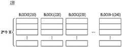
参考图2,存储器装置150可以包括多个存储器块BLOCK0(210)、BLOCK1(220)、BLOCK2(230)以及BLOCKN-1(240)。存储器块210、220、230和240中的每一个可以包括多个页,例如,2M个页,页的数目可以根据电路设计而变化。例如,在一些应用中,每个存储器块可以包括M个页。每个页可以包括耦合到字线WL的多个存储器单元。2, thememory device 150 may include a plurality of memory blocks BLOCK0 (210), BLOCK1 (220), BLOCK2 (230), and BLOCKN-1 (240). Each of the memory blocks 210, 220, 230, and 240 may include a plurality of pages, eg,2M pages, and the number of pages may vary according to circuit design. For example, in some applications, each memory block may include M pages. Each page may include multiple memory cells coupled to word lines WL.

存储器装置150不仅可以包括多级单元(MLC)存储器块(每个MLC存储器块包括由能够在一个存储器单元中存储两位数据的存储器单元实现的多个页),而且还可以包括三级单元(TLC)存储器块(每个TLC存储器块包括由能够在一个存储器单元中存储三位数据的存储器单元实现的多个页)、四级单元(QLC)存储器块(每个QLC存储器块包括由能够在一个存储器单元中存储四位数据的存储器单元实现的多个页)和/或更高级别的单元存储器块(每个存储器块包括由能够在一个存储器单元中存储五位或更多位数据的存储器单元实现的多个页)。Memory device 150 may include not only multi-level cell (MLC) memory blocks (each MLC memory block including multiple pages implemented by memory cells capable of storing two bits of data in one memory cell), but also three-level cells ( TLC) memory blocks (each TLC memory block includes multiple pages implemented by memory cells capable of storing three bits of data in one memory cell), quad-level cell (QLC) memory blocks (each QLC memory block includes Multiple pages implemented by memory cells that store four bits of data in one memory cell) and/or higher-level cell memory blocks (each memory block consists of memory capable of storing five or more bits of data in one memory cell multiple pages of the cell implementation).

根据本发明的实施例,存储器装置150被描述为非易失性存储器,诸如闪存,例如NAND闪存。然而,存储器装置150可以被实现为相变随机存取存储器(PCRAM)、电阻式随机存取存储器(RRAM或ReRAM)、铁电随机存取存储器(FRAM)、自旋转移力矩磁性随机存取存储器(STT-RAM或STT-MRAM)中的任一个。According to an embodiment of the present invention, thememory device 150 is described as a non-volatile memory, such as flash memory, eg, NAND flash memory. However, thememory device 150 may be implemented as phase change random access memory (PCRAM), resistive random access memory (RRAM or ReRAM), ferroelectric random access memory (FRAM), spin transfer torque magnetic random access memory (STT-RAM or STT-MRAM).

存储器块210、220、230、…240可以通过编程操作来存储从主机102传输的数据,并且通过读取操作将存储在其中的数据传输至主机102。The memory blocks 210 , 220 , 230 , . . . 240 may store data transferred from thehost 102 through programming operations and transfer data stored therein to thehost 102 through read operations.

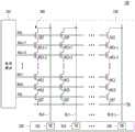
参考图3,可以与存储器系统110的存储器装置150中的多个存储器块152至156中的任一个相对应的存储器块330可以包括耦合到多个对应位线BL0至BLm-1的多个单元串340。每一列的单元串340可以包括一个或多个漏极选择晶体管DST和一个或多个源极选择晶体管SST。在漏极选择晶体管DST和源极选择晶体管SST之间,多个存储器单元或存储器单元晶体管MC0至MCn-1可以串联耦合。在一个实施例中,存储器单元MC0至MCn-1中的每一个可以由能够存储多个位的数据信息的MLC来体现。单元串340中的每一个可以电耦合到多个位线BL0至BLm-1之中的对应位线。例如,如图3所示,第一单元串耦合到第一位线BL0,并且最后单元串耦合到最后位线BLm-1。为了参考,在图3中,“DSL”表示漏极选择线、“SSL”表示源极选择线、且“CSL”表示公共源极线。3, a memory block 330, which may correspond to any of a plurality of memory blocks 152-156 in thememory device 150 of thememory system 110, may include a plurality of cells coupled to a plurality of corresponding bit lines BL0-BLm-1String 340. Thecell string 340 of each column may include one or more drain select transistors DST and one or more source select transistors SST. A plurality of memory cells or memory cell transistors MC0 to MCn- 1 may be coupled in series between the drain select transistor DST and the source select transistor SST. In one embodiment, each of the memory cells MC0 through MCn-1 may be embodied by an MLC capable of storing multiple bits of data information. Each of the cell strings 340 may be electrically coupled to a corresponding bit line among the plurality of bit lines BL0 to BLm-1. For example, as shown in FIG. 3, the first cell string is coupled to the first bit line BL0, and the last cell string is coupled to the last bit line BLm-1. For reference, in FIG. 3, "DSL" denotes a drain select line, "SSL" denotes a source select line, and "CSL" denotes a common source line.

尽管图3图示了NAND闪存单元,但是本发明不限于该方式。注意,存储器单元可以是NOR闪存单元、或者是包括组合在其中的两个或更多个种类的存储器单元的混合闪存单元。此外,应注意,存储器装置150可以是包括导电浮栅作为电荷存储层的闪存装置或包括绝缘层作为电荷存储层的电荷捕获闪存(CTF)装置。Although Figure 3 illustrates a NAND flash memory cell, the invention is not limited in this manner. Note that the memory cells may be NOR flash cells, or hybrid flash cells including two or more kinds of memory cells combined therein. Furthermore, it should be noted that thememory device 150 may be a flash memory device including a conductive floating gate as a charge storage layer or a charge trap flash (CTF) device including an insulating layer as a charge storage layer.

存储器装置150可以进一步包括电压供应310,电压供应310根据操作模式将包括编程电压、读取电压和通过电压的字线电压提供给字线。电压供应310的电压生成操作可以由控制电路(未示出)控制。在控制电路的控制下,电压供应310可以选择存储器单元阵列的存储器块(或扇区)中的一个,选择所选择的存储器块的字线中的一个并且根据需要将字线电压提供给所选择的字线和未选择的字线。Thememory device 150 may further include avoltage supply 310 that provides word line voltages including program voltages, read voltages, and pass voltages to word lines according to an operation mode. The voltage generating operation of thevoltage supply 310 may be controlled by a control circuit (not shown). Under the control of the control circuit, thevoltage supply 310 may select one of the memory blocks (or sectors) of the memory cell array, select one of the word lines of the selected memory block and provide the word line voltage to the selected memory block as needed word lines and unselected word lines.

存储器装置150可以包括由控制电路控制的读取和写入(读取/写入)电路320。在验证/正常读取操作期间,读取/写入电路320可以作为用于从存储器单元阵列读取数据的感测放大器进行操作。在编程操作期间,读取/写入电路320可以作为用于根据待存储在存储器单元阵列中的数据来驱动位线的写入驱动器进行操作。在编程操作期间,读取/写入电路320可以从缓冲器(未示出)接收待存储到存储器单元阵列中的数据,并且根据所接收的数据来驱动位线。读取/写入电路320可以包括分别对应于列(或位线)或列对(或位线对)的多个页缓冲器322至326,并且页缓冲器322至326中的每一个可以包括多个锁存器(未示出)。Memory device 150 may include read and write (read/write)circuitry 320 controlled by control circuitry. During verify/normal read operations, the read/write circuit 320 may operate as a sense amplifier for reading data from the memory cell array. During a programming operation, the read/write circuit 320 may operate as a write driver for driving bit lines according to data to be stored in the memory cell array. During a programming operation, the read/write circuit 320 may receive data to be stored into the memory cell array from a buffer (not shown) and drive bit lines according to the received data. The read/write circuit 320 may include a plurality ofpage buffers 322 to 326 corresponding to columns (or bit lines) or column pairs (or bit line pairs), respectively, and each of the page buffers 322 to 326 may include A plurality of latches (not shown).

存储器装置150可以由二维(2D)或三维(3D)存储器装置体现。特别地,如图4所示,存储器装置150可以由具有3D堆叠结构的非易失性存储器装置来体现。当存储器装置150具有3D结构时,多个存储器块BLOCK0至BLOCKN-1中的每一个也可以具有3D结构。Memory device 150 may be embodied by a two-dimensional (2D) or three-dimensional (3D) memory device. In particular, as shown in FIG. 4, thememory device 150 may be embodied by a non-volatile memory device having a 3D stack structure. When thememory device 150 has a 3D structure, each of the plurality of memory blocks BLOCK0 to BLOCKN-1 may also have a 3D structure.

存储器装置150中包括的每个存储器块330可以包括在第二方向上延伸的多个NAND串NS、以及在第一方向和第三方向上延伸的多个NAND串NS(未示出)。每个NAND串NS可以耦合到位线BL、至少一个漏极选择线DSL、至少一个源极选择线SSL、多个字线WL、至少一个虚设字线DWL(未示出)和公共源极线CSL,并且每个NAND串NS可以包括多个晶体管结构。Each memory block 330 included in thememory device 150 may include a plurality of NAND strings NS extending in the second direction, and a plurality of NAND strings NS (not shown) extending in the first and third directions. Each NAND string NS may be coupled to a bit line BL, at least one drain select line DSL, at least one source select line SSL, a plurality of word lines WL, at least one dummy word line DWL (not shown), and a common source line CSL , and each NAND string NS may include a plurality of transistor structures.

简而言之,存储器装置150的每个存储器块330可以耦合到多个位线BL、多个漏极选择线DSL、多个源极选择线SSL、多个字线WL、多个虚设字线DWL和多个公共源极线CSL,并且每个存储器块330可以包括多个NAND串NS。此外,在每个存储器块330中,一个位线BL可以耦合到多个NAND串NS,以在一个NAND串NS中实现多个晶体管。而且,每个NAND串NS的漏极选择晶体管DST可以耦合到对应的位线BL,并且每个NAND串NS的源极选择晶体管SST可以耦合到公共源极线CSL。存储器单元MC可以设置在每个NAND串NS的漏极选择晶体管DST和源极选择晶体管SST之间。换言之,可以在存储器装置150的每个存储器块330中实现多个存储器单元。In short, each memory block 330 ofmemory device 150 may be coupled to multiple bit lines BL, multiple drain select lines DSL, multiple source select lines SSL, multiple word lines WL, multiple dummy word lines DWL and a plurality of common source lines CSL, and each memory block 330 may include a plurality of NAND strings NS. Furthermore, in each memory block 330, one bit line BL may be coupled to multiple NAND strings NS to implement multiple transistors in one NAND string NS. Also, the drain select transistor DST of each NAND string NS may be coupled to the corresponding bit line BL, and the source select transistor SST of each NAND string NS may be coupled to the common source line CSL. The memory cell MC may be disposed between the drain selection transistor DST and the source selection transistor SST of each NAND string NS. In other words, multiple memory cells may be implemented in each memory block 330 of thememory device 150 .

如参考图1所描述,存储器144可以在处理器134的控制下使用表来管理每个映射段和每个映射数据。例如,如图5A和图5B所示,关于映射段的信息可以存储在第一表510中,并且关于映射数据的信息可以存储在第二表530中。参考图5A至图5B来描述第一表510和第二表530。As described with reference to FIG. 1 , thememory 144 may manage each mapped segment and each mapped data using a table under the control of theprocessor 134 . For example, as shown in FIGS. 5A and 5B , information about mapping segments may be stored in the first table 510 , and information about mapping data may be stored in the second table 530 . The first table 510 and the second table 530 are described with reference to FIGS. 5A to 5B .

图5A是图示根据实施例的第一表510的结构的图。FIG. 5A is a diagram illustrating the structure of the first table 510 according to an embodiment.

参考图5A,第一表510可以表示映射段与包括多个逻辑地址的逻辑地址组之间的映射关系(第一映射)。多个第一映射信息可以存储在第一表510中。第一映射信息可以包括映射段、逻辑地址或逻辑块地址(LBA)以及第一标志信息(Flag)。第一标志信息可以指示第一映射是否被执行。第一表510指示具有第一标志信息“M”的第一映射段与包括第1至第K逻辑地址LBA<1:K>的第一逻辑组进行映射。此外,第一表510指示具有第一标志信息“U”的第二映射段未与包括第(K+1)至第2K逻辑地址LBA<K+1:2K>的第二逻辑地址进行映射。类似地,第一表510针对其余映射段中的每一个而指示是否与对应逻辑地址进行映射。Referring to FIG. 5A , the first table 510 may represent a mapping relationship (first mapping) between a mapping segment and a logical address group including a plurality of logical addresses. A plurality of first mapping information may be stored in the first table 510 . The first mapping information may include a mapping segment, a logical address or a logical block address (LBA), and first flag information (Flag). The first flag information may indicate whether the first mapping is performed. The first table 510 indicates that the first mapped segment having the first flag information 'M' is mapped with the first logical group including the 1st to Kth logical addresses LBA<1:K>. Also, the first table 510 indicates that the second mapped segment having the first flag information 'U' is not mapped with the second logical addresses including the (K+1)th to 2Kth logical addresses LBA<K+1:2K>. Similarly, the first table 510 indicates, for each of the remaining mapped segments, whether to map with the corresponding logical address.

图5B是图示根据实施例的第二表530的结构的图。FIG. 5B is a diagram illustrating the structure of the second table 530 according to an embodiment.

参考图5B,第二表530可以表示逻辑地址信息和物理地址信息之间的映射关系(第二映射)。多个第二映射信息可以存储在第二表530中。第二映射信息可以包括逻辑地址(LBA)、物理地址(PBA)和第二标志信息(Flag)。第二标志信息可以指示第二映射是否被执行。例如,第二表530可以指示具有第二标志信息“M”的第1逻辑地址LBA 1与第56物理地址PBA56进行映射。此外,第二表530可以指示具有第二标志信息“U”的第三逻辑地址LBA3没有与第11物理地址PBA 11进行映射。类似地,第二表530针对其余逻辑地址中的每一个而指示是否与对应的物理地址进行映射。Referring to FIG. 5B , the second table 530 may represent a mapping relationship between logical address information and physical address information (second mapping). A plurality of second mapping information may be stored in the second table 530 . The second mapping information may include a logical address (LBA), a physical address (PBA), and second flag information (Flag). The second flag information may indicate whether the second mapping is performed. For example, the second table 530 may indicate that the first logical address LBA1 having the second flag information 'M' is mapped with the 56th physical address PBA56. Also, the second table 530 may indicate that the third logical address LBA3 having the second flag information 'U' is not mapped with the 11th physical address PBA11. Similarly, the second table 530 indicates, for each of the remaining logical addresses, whether to map with the corresponding physical address.

第二表530基于映射段表示第二映射信息。第二表530表示与第一映射段进行映射的第1至第K逻辑地址中的每一个的第二映射信息。虽然图5B仅图示与第一映射段映射的第1至第K逻辑地址中的每一个的第二映射信息,但是这仅是示例,并且第二表530可以针对多个映射段中的每一个来被配置。The second table 530 represents the second mapping information based on the mapping segment. The second table 530 represents the second mapping information of each of the 1st to Kth logical addresses mapped with the first mapping segment. Although FIG. 5B only illustrates the second mapping information of each of the 1st to Kth logical addresses mapped with the first mapping segment, this is only an example, and the second table 530 may be for each of the plurality of mapping segments one to be configured.

图5A和图5B中所示的第一表510和第二表530可以在处理器134的控制下分别存储在存储器装置150中。The first table 510 and the second table 530 shown in FIGS. 5A and 5B may be stored in thememory device 150 under the control of theprocessor 134, respectively.

再次参考图1,处理器134可以将第一表510和第二表530从存储器装置150加载到存储器144中,以对从主机102提供的取消映射命令进行处理。Referring again to FIG. 1 , theprocessor 134 may load the first table 510 and the second table 530 from thememory device 150 into thememory 144 to process the unmap command provided from thehost 102 .

取消映射管理器146可以参考存储在存储器144中的第一表510和第二表530来处理从主机102提供的取消映射命令。取消映射管理器146可以根据从主机102提供的取消映射命令来执行对第一映射和/或第二映射进行取消映射的取消映射操作。特别地,根据本实施例的存储器系统110可以针对多个逻辑地址根据取消映射命令来有效地执行取消映射操作。下面详细描述根据实施例的存储器系统110的操作。Theunmap manager 146 may refer to the first table 510 and the second table 530 stored in thememory 144 to process the unmap command provided from thehost 102 . Theunmap manager 146 may perform an unmap operation to unmap the first map and/or the second map in accordance with the unmap command provided from thehost 102 . In particular, thememory system 110 according to the present embodiment can efficiently perform an unmap operation according to an unmap command for a plurality of logical addresses. The operation of thememory system 110 according to an embodiment is described in detail below.

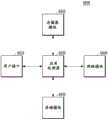
图6A至图6E是图示根据实施例的存储器系统110的操作的图。例如,假设每个映射段与100个逻辑地址进行映射。此外,假设第一映射段与第1至第100逻辑地址进行映射,并且第二映射段与第101至第200逻辑地址进行映射。以相同的方式,假设第三映射段至第十一映射段中的每一个与100个逻辑地址的对应组进行映射。假设针对从主机102提供的取消映射命令的映射数据的整体大小大于或等于可以被预先确定的阈值。以下描述的存储器系统110的操作仅是一个示例。6A-6E are diagrams illustrating the operation of thememory system 110 according to an embodiment. For example, suppose each mapped segment is mapped with 100 logical addresses. Also, it is assumed that the first mapped segment is mapped with the 1st to 100th logical addresses, and the second mapped segment is mapped with the 101st to 200th logical addresses. In the same manner, it is assumed that each of the third to eleventh mapped segments is mapped with a corresponding group of 100 logical addresses. It is assumed that the overall size of the map data for the unmap command provided from thehost 102 is greater than or equal to a threshold value that can be predetermined. The operation of thememory system 110 described below is but one example.

参考图6A,主机102可以向存储器系统110提供针对第10至第1050逻辑地址LBA<10:1050>的取消映射命令。当从主机102接收取消映射命令时,控制器130的处理器134可以从存储器装置150加载与目标逻辑地址相关联的第一映射信息和第二映射信息。目标逻辑地址指示第10至第1050逻辑地址LBA<10:1050>。换言之,处理器134可以从存储器装置150读取关于第一映射段至第十一映射段的第一映射信息以及关于第10至第1050逻辑地址LBA<10:1050>中的每个逻辑地址的第二映射信息,并且将第一映射信息和第二映射信息存储在存储器144中。另外,处理器134可以从存储器装置150加载分别存储有第一映射信息和第二映射信息的第一表610和第二表630。特别地,即使第一映射信息和第二映射信息已存储在存储器144中,处理器134也可以从存储器装置150读取第一映射信息和第二映射信息,并且将所读取的信息再次存储在存储器144中。由于存储在存储器装置150中的第一映射信息和第二映射信息是最近更新的信息,当接收取消映射命令时,处理器134可以从存储器装置150加载第一映射信息和第二映射信息。Referring to FIG. 6A , thehost 102 may provide an unmap command to thememory system 110 for the 10th to 1050th logical addresses LBA<10:1050>. When receiving an unmap command fromhost 102 ,processor 134 ofcontroller 130 may load first and second mapping information associated with the target logical address frommemory device 150 . The target logical addresses indicate 10th to 1050th logical addresses LBA<10:1050>. In other words, theprocessor 134 may read, from thememory device 150 , the first mapping information about the first to eleventh mapped segments and the information about each of the 10th to 1050th logical addresses LBA<10:1050>. second mapping information, and the first mapping information and the second mapping information are stored in thememory 144 . Additionally, theprocessor 134 may load from thememory device 150 the first table 610 and the second table 630 storing the first mapping information and the second mapping information, respectively. In particular, even if the first mapping information and the second mapping information have been stored in thememory 144, theprocessor 134 may read the first mapping information and the second mapping information from thememory device 150 and store the read information again inmemory 144. Since the first mapping information and the second mapping information stored in thememory device 150 are the most recently updated information, theprocessor 134 may load the first mapping information and the second mapping information from thememory device 150 when receiving the unmap command.

参考图6B,取消映射管理器146可以将从主机102提供的取消映射命令的映射数据的整体大小与阈值进行比较。阈值可以根据系统或处理考虑来设置。当针对取消映射命令的映射数据的整体大小大于或等于阈值时,取消映射管理器146可以基于存储在存储器144中的第一表610,将多个映射段分类为第一区域(例如,头部区域)、第二区域(例如,主体区域)和第三区域(例如,尾部区域)。Referring to FIG. 6B , theunmap manager 146 may compare the overall size of the map data for the unmap command provided from thehost 102 to a threshold. Thresholds can be set based on system or processing considerations. When the overall size of the map data for the unmap command is greater than or equal to the threshold, theunmap manager 146 may classify the plurality of map segments into the first region (eg, the header) based on the first table 610 stored in thememory 144 region), second region (eg, body region), and third region (eg, tail region).

具体地,取消映射管理器146可以将映射段分类为第一区域或第三区域。第一区域或第三区域中的映射段可以与其中多个逻辑地址中只有一些是目标逻辑地址的逻辑组进行映射。另一方面,取消映射管理器146可以将映射段分类到第二区域中。第二区域中的映射段可以与其中所有逻辑地址都是目标逻辑地址的逻辑组进行映射。例如,取消映射管理器146可以将第一映射片段分类到第一区域(或头部区域)中。第一映射段可以与包括第10逻辑地址LBA 10(其是目标逻辑地址的起始逻辑地址)的逻辑组进行映射。取消映射管理器146可以将第11映射段分类到第三区域(或尾部区域)中。第11映射段可以与包括第1050逻辑地址LBA 1050(其是目标逻辑地址的最后逻辑地址)的逻辑组进行映射。取消映射管理器146可以将第二至第十映射段分类到第二区域(或主体区域)中。Specifically, theunmap manager 146 may classify the mapped segment as a first area or a third area. The mapped segment in the first region or the third region may be mapped with a logical group in which only some of the plurality of logical addresses are target logical addresses. On the other hand, theunmap manager 146 may sort the mapped segment into the second area. The mapped segment in the second region can be mapped with a logical group in which all logical addresses are target logical addresses. For example, theunmap manager 146 may classify the first mapped segment into the first region (or header region). The first mapped segment may be mapped with a logical group including the 10thlogical address LBA 10, which is the starting logical address of the target logical address. Theunmap manager 146 may classify the 11th mapped segment into the third region (or tail region). The 11th mapped segment may be mapped with a logical group including the 1050thlogical address LBA 1050, which is the last logical address of the target logical address. Theunmap manager 146 may classify the second through tenth mapped segments into the second area (or body area).

取消映射管理器146可以以不同的方式在第一区域至第三区域上执行取消映射操作。Theunmap manager 146 may perform the unmap operation on the first to third regions in different ways.

参考图6C,取消映射管理器146可以针对多个逻辑地址(其被包括在与第一区域中的第一映射段进行映射的逻辑组中)之中的目标逻辑地址的第二映射执行取消映射操作。在图6C中,第二表630_1指示在执行取消映射操作之前的第二表630的状态,并且第二表630_3指示在执行取消映射操作之后的第二表630的状态。具体地,与第一映射段映射的逻辑组中包括的多个逻辑地址之中的目标逻辑地址是第10逻辑地址LBA 10至第100逻辑地址LBA 100。取消映射管理器146可以根据取消映射命令,将第10逻辑地址LBA 10至第100逻辑地址LBA 100中的每个逻辑地址的第二映射独立地取消映射。取消映射管理器146可以将与存储在第二表630_3中的第10逻辑地址LBA 10至第100逻辑地址LBA 100中的每一个相对应的第二标志信息从“M”更新为“U”。处理器134可以在存储器装置150中存储第二表630_3,其中存储了关于第10逻辑地址LBA 10至第100逻辑地址LBA 100中的每一个的取消映射信息。Referring to FIG. 6C , theunmap manager 146 may perform unmap for the second mapping of the target logical address among the plurality of logical addresses included in the logical group mapped with the first mapped segment in the first region operate. In FIG. 6C , the second table 630_1 indicates the state of the second table 630 before the unmap operation is performed, and the second table 630_3 indicates the state of the second table 630 after the unmap operation is performed. Specifically, the target logical addresses among the plurality of logical addresses included in the logical group mapped with the first mapping segment are the 10th logical address LBA10 to the 100th logical address LBA100. Theunmap manager 146 may independently unmap the second mapping of each logical address of the 10thlogical address LBA 10 to the 100thlogical address LBA 100 according to the unmap command. Theunmap manager 146 may update the second flag information corresponding to each of the 10th logical address LBA10 to the 100th logical address LBA100 stored in the second table 630_3 from "M" to "U". Theprocessor 134 may store the second table 630_3 in thememory device 150 in which unmapping information about each of the 10thlogical address LBA 10 to the 100thlogical address LBA 100 is stored.

参考图6D,取消映射管理器146可以对第二区域中的第二映射段至第十映射段中的每一个的第一映射执行取消映射操作。在图6D中,第一表610_1指示在执行取消映射操作之前的第一表610的状态,并且第一表610_3指示在执行取消映射操作之后的第一表610的状态。与第二区域中的多个映射段中的每一个进行映射的逻辑组中包括的多个逻辑地址均被包括在目标逻辑地址中。换言之,映射到第二映射段至第十映射段中的每一个的逻辑组可以包括作为目标逻辑地址中的一些的第101至第1000逻辑地址LBA<101:1000>。因此,取消映射管理器146不像第一区域那样针对第二映射执行取消映射操作。Referring to FIG. 6D , theunmap manager 146 may perform an unmap operation on the first mapping of each of the second mapped segment to the tenth mapped segment in the second region. In FIG. 6D , the first table 610_1 indicates the state of the first table 610 before the unmap operation is performed, and the first table 610_3 indicates the state of the first table 610 after the unmap operation is performed. The plurality of logical addresses included in the logical group mapped with each of the plurality of mapped segments in the second area are included in the target logical address. In other words, the logical group mapped to each of the second to tenth mapped segments may include the 101st to 1000th logical addresses LBA<101:1000> as some of the target logical addresses. Therefore, theunmap manager 146 does not perform an unmap operation for the second map as the first region does.

在该情况下,取消映射管理器146可以对第二映射段至第十映射段中的每一个的第一映射进行取消映射。换言之,取消映射管理器146可以基于第一表610_1,去除第二映射段与第101至第200逻辑地址LBA<101:200>之间的映射关系。另外,取消映射管理器146可以去除第三映射段与第201至第300逻辑地址LBA<201:300>之间的映射关系。以相同的方式,取消映射管理器146可以去除与第四映射段至第十映射段中的每一个进行映射的多个逻辑地址之间的映射关系。In this case, theunmap manager 146 may unmap the first mapping of each of the second through tenth mapped segments. In other words, theunmap manager 146 may remove the mapping relationship between the second mapped segment and the 101st to 200th logical addresses LBA<101:200> based on the first table 610_1. In addition, theunmap manager 146 may remove the mapping relationship between the third mapped segment and the 201st to 300th logical addresses LBA<201:300>. In the same manner, theunmap manager 146 may remove the mapping relationship between the plurality of logical addresses mapped with each of the fourth to tenth mapped segments.

当第101逻辑地址LBA 101至第1000逻辑地址LBA 1000中的每一个的第二映射要被取消映射时,必须执行总共900个取消映射操作。然而,取消映射管理器146可以通过对多个映射段中的每一个的第一映射进行取消映射来执行总共9个取消映射操作。When the second mapping of each of the 101stlogical address LBA 101 to the 1000thlogical address LBA 1000 is to be unmapped, a total of 900 unmap operations must be performed. However, theunmap manager 146 may perform a total of nine unmap operations by unmapping the first mapping of each of the plurality of mapped segments.

取消映射管理器146可以将第一标志信息从“M”更新为“U”。第一标志信息可以对应于存储在第一表610_1中的第二映射段至第十映射段中的每一个。处理器134可以在存储器装置150中存储第一表610_1,其中存储了关于第二映射段至第十映射段中的每一个的取消映射信息。处理器134可以在存储器装置150中不存储第二表,其中存储了与第二映射段至第十映射段中的每一个相对应的映射数据。Theunmap manager 146 may update the first flag information from "M" to "U". The first flag information may correspond to each of the second to tenth mapping sections stored in the first table 610_1. Theprocessor 134 may store the first table 610_1 in thememory device 150 in which unmap information regarding each of the second to tenth mapped segments is stored. Theprocessor 134 may not store the second table in thememory device 150 in which mapping data corresponding to each of the second to tenth mapping segments is stored.

参考图6E,取消映射管理器146可以针对与多个逻辑地址(其被包括在与第三区域中的第十一映射段进行映射的逻辑组中)之中与目标逻辑地址相对应的逻辑地址的第二映射执行取消映射操作。在图6E中,第二表630_5指示在执行取消映射操作之前的第二表630的状态,并且第二表630_7指示在执行取消映射操作之后的第二表630的状态。具体地,与第十一映射段映射的逻辑组中包括的多个逻辑地址之中的目标逻辑地址是第1001逻辑地址LBA1001至第1050逻辑地址LBA 1050。取消映射管理器146可以根据取消映射命令,对第1001逻辑地址LBA 1001至第1050逻辑地址LBA 1050中的每一个的第二映射进行取消映射。此外,取消映射管理器146可以将第二标志信息从“M”更新为“U”。第二标志信息可以对应于存储在第二表630_5中的第1001逻辑地址LBA1001至第1050逻辑地址LBA 1050。处理器134可以在存储器装置150中存储第二表630_7,其中存储有关于第1001逻辑地址LBA 1001至第1050逻辑地址LBA 1050的取消映射信息。Referring to FIG. 6E , theunmap manager 146 may target the logical address corresponding to the target logical address among the plurality of logical addresses included in the logical group mapped with the eleventh mapped segment in the third region The second map performs an unmap operation. In FIG. 6E , the second table 630_5 indicates the state of the second table 630 before the unmap operation is performed, and the second table 630_7 indicates the state of the second table 630 after the unmap operation is performed. Specifically, the target logical addresses among the plurality of logical addresses included in the logical group mapped with the eleventh mapping segment are the 1001st logical address LBA1001 to the 1050th logical address LBA1050. Theunmap manager 146 may unmap the second mapping of each of the 1001stlogical address LBA 1001 to the 1050thlogical address LBA 1050 according to the unmap command. Also, theunmap manager 146 may update the second flag information from "M" to "U". The second flag information may correspond to the 1001st logical address LBA1001 to the 1050th logical address LBA1050 stored in the second table 630_5. Theprocessor 134 may store the second table 630_7 in thememory device 150 in which unmapping information about the 1001stlogical address LBA 1001 to the 1050thlogical address LBA 1050 is stored.

尽管未示出,但是当针对从主机102提供的取消映射命令的映射数据的整体大小小于阈值时,取消映射管理器146可以执行对目标逻辑地址的第二映射进行取消映射的操作。在这种情况下,取消映射管理器146不执行对第一映射进行取消映射的操作。Although not shown, when the overall size of the map data for the unmap command provided from thehost 102 is less than a threshold, theunmap manager 146 may perform an operation to unmap the second map of the target logical address. In this case, theunmap manager 146 does not perform an operation to unmap the first map.

图7是图示根据实施例的存储器系统110的操作过程的流程图。特别地,图7图示了存储器系统110对从主机102接收的取消映射命令进行处理的过程。FIG. 7 is a flowchart illustrating an operation process of thememory system 110 according to an embodiment. In particular, FIG. 7 illustrates the process by whichmemory system 110 processes an unmap command received fromhost 102 .

参考图7,在步骤S701中,处理器134可以从存储器装置150加载第一映射信息和第二映射信息,并且将所加载的信息存储在存储器144中。Referring to FIG. 7 , in step S701 , theprocessor 134 may load the first mapping information and the second mapping information from thememory device 150 and store the loaded information in thememory 144 .

在步骤S703中,取消映射管理器146可以将与目标逻辑地址相对应的映射数据(即,目标映射数据)的整体大小与可以被预先确定的阈值进行比较。In step S703, theunmap manager 146 may compare the overall size of the mapping data corresponding to the target logical address (ie, the target mapping data) with a threshold value that may be predetermined.

当确定目标映射数据的整体大小大于或等于阈值时(即,在步骤S703中为“是”),在步骤S705中,取消映射管理器146可以将多个映射段分类(或划分)到多个区域或组中。例如,取消映射管理器146可以将多个映射段分类为第一、第二和第三组或区域。如参考图6B所描述,取消映射管理器146可以将映射段分类为第一区域或第三区域。第一区域和第三区域的映射段可以与其中多个逻辑地址中的一些是目标逻辑地址的逻辑组进行映射。取消映射管理器146可以将映射段分类到第二区域中。第二区域的映射段可以与其中所有逻辑地址都是目标逻辑地址的逻辑组进行映射。When it is determined that the overall size of the target mapping data is greater than or equal to the threshold (ie, YES in step S703 ), in step S705 , theunmap manager 146 may classify (or divide) the plurality of mapped segments into a plurality of area or group. For example, theunmap manager 146 may classify the plurality of mapped segments into first, second, and third groups or regions. As described with reference to FIG. 6B , theunmap manager 146 may classify the mapped segment into a first area or a third area. The mapped segments of the first region and the third region may be mapped with a logical group in which some of the plurality of logical addresses are target logical addresses. Theunmap manager 146 may sort the mapped segment into the second area. The mapped segment of the second region may be mapped with a logical group in which all logical addresses are target logical addresses.

在步骤S707中,取消映射管理器146可以针对多个逻辑地址(其被包括在与第一区域和第三区域中包括的映射段进行映射的逻辑组中)之中的目标逻辑地址的第二映射执行取消映射操作。In step S707, theunmap manager 146 may target the second one of the target logical address among the plurality of logical addresses included in the logical group mapped with the mapped segments included in the first area and the third area. The map performs an unmap operation.

在步骤S709中,处理器134可以在存储器装置150中存储关于在步骤S707中执行取消映射操作的每个目标逻辑地址的第二映射信息。另外,处理器134可以在存储器装置150中存储其中存储有第二映射信息的第二表。In step S709, theprocessor 134 may store second mapping information in thememory device 150 for each target logical address for which the unmap operation was performed in step S707. Additionally, theprocessor 134 may store in the memory device 150 a second table having the second mapping information stored therein.

在步骤S711中,取消映射管理器146可以针对第二区域中包括的映射段的第一映射执行取消映射操作。In step S711, theunmap manager 146 may perform an unmap operation with respect to the first mapping of the mapped segment included in the second area.

在步骤S713中,处理器134可以在存储器装置150中存储关于在步骤S711中执行取消映射操作的映射段的第一映射信息。另外,处理器134可以将记录有第一映射信息的第二表存储在存储器装置150中。In step S713, theprocessor 134 may store in thememory device 150 the first mapping information about the mapped segment on which the unmap operation was performed in step S711. In addition, theprocessor 134 may store the second table in which the first mapping information is recorded in thememory device 150 .

当确定目标映射数据的整体大小小于阈值时(即,在步骤S703中为“否”),在步骤S715中,取消映射管理器146可以针对目标逻辑地址的第二映射执行取消映射操作。When it is determined that the overall size of the target map data is less than the threshold (ie, "NO" in step S703), in step S715, theunmap manager 146 may perform an unmap operation for the second mapping of the target logical address.

在步骤S717中,处理器134可以在存储器装置150中存储关于在步骤S715中执行取消映射操作的每个目标逻辑地址的第二映射信息。另外,处理器134可以在存储器装置150中存储其中存储有第二映射信息的第二表。In step S717, theprocessor 134 may store the second mapping information in thememory device 150 for each target logical address for which the unmap operation was performed in step S715. Additionally, theprocessor 134 may store in the memory device 150 a second table having the second mapping information stored therein.

图8至图16是示意性地图示根据各种实施例的图1至图7的数据处理系统的应用示例的图。8 to 16 are diagrams schematically illustrating application examples of the data processing systems of FIGS. 1 to 7 according to various embodiments.

图8是示意性地图示根据实施例的包括存储器系统的数据处理系统的图。例如,图8示意性地图示了应用根据实施例的存储器系统的存储器卡系统6100。FIG. 8 is a diagram schematically illustrating a data processing system including a memory system according to an embodiment. For example, FIG. 8 schematically illustrates amemory card system 6100 to which a memory system according to an embodiment is applied.

参考图8,存储器卡系统6100可以包括存储器控制器6120、存储器装置6130和连接器6110。Referring to FIG. 8 , thememory card system 6100 may include amemory controller 6120 , amemory device 6130 and aconnector 6110 .

更具体地,存储器控制器6120可以连接到由非易失性存储器(NVM)体现的存储器装置6130并且被配置为访问存储器装置6130。例如,存储器控制器6120可以被配置为控制存储器装置6130的读取、写入、擦除和后台操作。存储器控制器6120可以被配置为提供存储器装置6130和主机(未示出)之间的接口,并且驱动固件以用于控制存储器装置6130。即,存储器控制器6120可以对应于参考图1描述的存储器系统110的控制器130,并且存储器装置6130可以对应于参考图1描述的存储器系统110的存储器装置150。More specifically, thememory controller 6120 may be connected to thememory device 6130 embodied by non-volatile memory (NVM) and configured to access thememory device 6130 . For example,memory controller 6120 may be configured to control read, write, erase, and background operations ofmemory device 6130. Thememory controller 6120 may be configured to provide an interface between thememory device 6130 and a host (not shown), and to drive firmware for controlling thememory device 6130 . That is, thememory controller 6120 may correspond to thecontroller 130 of thememory system 110 described with reference to FIG. 1 , and thememory device 6130 may correspond to thememory device 150 of thememory system 110 described with reference to FIG. 1 .

因此,如图1所示,存储器控制器6120可以包括随机存取存储器(RAM)、处理器、主机接口、存储器接口和纠错部件。Thus, as shown in FIG. 1,memory controller 6120 may include random access memory (RAM), a processor, a host interface, a memory interface, and error correction components.

存储器控制器6120可以通过连接器6110与外部装置(例如,图1的主机102)通信。例如,如参考图1所述,存储器控制器6120可以被配置为通过各种通信协议(诸如通用串行总线(USB)、多媒体卡(MMC)、嵌入式MMC(eMMC)、外围部件互连(PCI)、PCI快速(PCIe)、高级技术附件(ATA)、串行ATA、并行ATA、小型计算机系统接口(SCSI)、增强型小型磁盘接口(EDSI)、集成驱动电子装置(IDE)、火线、通用闪存(UFS)、无线保真(Wi-Fi或WiFi)和蓝牙)中的一个或多个与外部装置通信。因此,根据实施例的存储器系统和数据处理系统可以应用于有线/无线电子装置或特别地应用于移动电子装置。Thememory controller 6120 may communicate with an external device (eg, thehost 102 of FIG. 1 ) through theconnector 6110 . For example, as described with reference to FIG. 1, thememory controller 6120 may be configured to communicate via various communication protocols such as Universal Serial Bus (USB), Multimedia Card (MMC), Embedded MMC (eMMC), Peripheral Component Interconnect ( PCI), PCI Express (PCIe), Advanced Technology Attachment (ATA), Serial ATA, Parallel ATA, Small Computer System Interface (SCSI), Enhanced Small Disk Interface (EDSI), Integrated Drive Electronics (IDE), FireWire, One or more of Universal Flash Memory (UFS), Wireless Fidelity (Wi-Fi or WiFi), and Bluetooth) to communicate with external devices. Therefore, the memory system and the data processing system according to the embodiments may be applied to wired/wireless electronic devices or particularly to mobile electronic devices.

存储器装置6130可以由非易失性存储器实现。例如,存储器装置6130可以由各种非易失性存储器装置(诸如可擦除可编程ROM(EPROM)、电可擦除可编程ROM(EEPROM)、NAND闪存、NOR闪存、相变RAM(PRAM)、电阻式RAM(ReRAM)、铁电式RAM(FRAM)和自旋转移力矩磁性RAM(STT-RAM))中的任一个来实现。Thememory device 6130 may be implemented by non-volatile memory. For example,memory device 6130 may be composed of various non-volatile memory devices such as erasable programmable ROM (EPROM), electrically erasable programmable ROM (EEPROM), NAND flash, NOR flash, phase-change RAM (PRAM) , Resistive RAM (ReRAM), Ferroelectric RAM (FRAM), and Spin Transfer Torque Magnetic RAM (STT-RAM)).

存储器控制器6120和存储器装置6130可以集成到单个半导体装置中。例如,存储器控制器6120和存储器装置6130可以被集成以形成固态驱动器(SSD)。而且,存储器控制器6120和存储器装置6130可以形成诸如PC卡(例如,个人计算机存储器卡国际协会(PCMCIA))、紧凑型闪存(CF)卡、智能媒体卡(例如,SM和SMC)、记忆棒、多媒体卡(例如,MMC、RS-MMC、MMCmicro和eMMC)、安全数字(SD)卡(例如,miniSD卡、microSD卡和SDHC卡)和通用闪存(UFS)的存储器卡。Thememory controller 6120 and thememory device 6130 may be integrated into a single semiconductor device. For example,memory controller 6120 andmemory device 6130 may be integrated to form a solid state drive (SSD). Also, thememory controller 6120 and thememory device 6130 may form forms such as PC cards (eg, Personal Computer Memory Card International Association (PCMCIA)), compact flash (CF) cards, smart media cards (eg, SM and SMC), memory sticks , Multimedia Cards (eg, MMC, RS-MMC, MMCmicro, and eMMC), Secure Digital (SD) Cards (eg, miniSD, microSD, and SDHC), and Universal Flash (UFS) memory cards.

图9是示意性图示根据实施例的包括存储器系统的数据处理系统6200的另一示例的图。FIG. 9 is a diagram schematically illustrating another example of adata processing system 6200 including a memory system, according to an embodiment.

参考图9,数据处理系统6200可以包括具有一个或多个非易失性存储器(NVM)的存储器装置6230和用于控制存储器装置6230的存储器控制器6220。如参考图1所描述,数据处理系统6200可以用作诸如存储器卡(CF卡、SD卡等)或USB装置的存储介质。存储器装置6230可以对应于图1所示的存储器系统110中的存储器装置150,并且存储器控制器6220可以对应于图1所示的存储器系统110中的控制器130。Referring to FIG. 9 , adata processing system 6200 may include amemory device 6230 having one or more non-volatile memories (NVMs) and amemory controller 6220 for controlling thememory device 6230 . As described with reference to FIG. 1, thedata processing system 6200 can be used as a storage medium such as a memory card (CF card, SD card, etc.) or a USB device. Thememory device 6230 may correspond to thememory device 150 in thememory system 110 shown in FIG. 1 , and thememory controller 6220 may correspond to thecontroller 130 in thememory system 110 shown in FIG. 1 .

存储器控制器6220可以响应于主机6210的请求来控制对存储器装置6230的读取、写入或擦除操作,并且存储器控制器6220可以包括一个或多个中央处理单元(CPU)6221、缓冲存储器(诸如随机存取存储器(RAM))6222、纠错码(ECC)电路6223、主机接口6224和存储器接口(诸如NVM接口)6225。Thememory controller 6220 may control read, write, or erase operations to thememory device 6230 in response to requests from thehost 6210, and thememory controller 6220 may include one or more central processing units (CPUs) 6221, buffer memory ( Such as random access memory (RAM) 6222, error correction code (ECC)circuit 6223,host interface 6224 and memory interface (such as NVM interface) 6225.

CPU 6221可以控制存储器装置6230上的整体操作(例如,读取、写入、文件系统管理和坏页管理操作)。RAM 6222可以根据CPU 6221的控制来操作,并且用作工作存储器、缓冲存储器或高速缓存存储器。当RAM 6222用作工作存储器时,由CPU 6221处理的数据可以被临时存储在RAM 6222中。当RAM 6222用作缓冲存储器时,RAM 6222可以用于缓冲从主机6210发送到存储器装置6230或从存储器装置6230发送到主机6210的数据。当RAM 6222用作高速缓存存储器时,RAM 6222可以辅助存储器装置6230以高速操作。CPU 6221 may control overall operations on memory device 6230 (eg, read, write, file system management, and bad page management operations). TheRAM 6222 can operate according to the control of theCPU 6221 and function as a work memory, a buffer memory, or a cache memory. When theRAM 6222 is used as a work memory, data processed by theCPU 6221 can be temporarily stored in theRAM 6222. WhenRAM 6222 is used as buffer memory,RAM 6222 may be used to buffer data sent fromhost 6210 tomemory device 6230 or frommemory device 6230 tohost 6210. WhenRAM 6222 is used as cache memory,RAM 6222 may assistmemory device 6230 to operate at high speed.

ECC电路6223可以对应于图1中所示的控制器130的ECC部件138。如参考图1所述,ECC电路6223可以生成用于纠正从存储器装置6230提供的数据的故障位或错误位的纠错码(ECC)。ECC电路6223可以对提供给存储器装置6230的数据执行纠错编码,从而形成具有奇偶校验位的数据。奇偶校验位可以存储在存储器装置6230中。ECC电路6223可以对从存储器装置6230输出的数据执行纠错解码。ECC电路6223可以使用奇偶校验位来纠正错误。例如,如参考图1所述,ECC电路6223可以使用低密度奇偶校验(LDPC)码、Bose-Chaudhri-Hocquenghem(BCH)码、turbo码、Reed-Solomon码、卷积码、递归系统代码(RSC)或编码调制(诸如网格编码调制(TCM)或块编码调制(BCM))来纠正错误。TheECC circuit 6223 may correspond to the ECC part 138 of thecontroller 130 shown in FIG. 1 . As described with reference to FIG. 1 , theECC circuit 6223 may generate an error correction code (ECC) for correcting faulty or erroneous bits of data provided from thememory device 6230 . TheECC circuit 6223 may perform error correction encoding on the data provided to thememory device 6230, thereby forming data having parity bits. Parity bits may be stored inmemory device 6230. TheECC circuit 6223 can perform error correction decoding on data output from thememory device 6230 . TheECC circuit 6223 can use parity bits to correct errors. For example, as described with reference to FIG. 1, theECC circuit 6223 may use Low Density Parity Check (LDPC) codes, Bose-Chaudhri-Hocquenghem (BCH) codes, turbo codes, Reed-Solomon codes, convolutional codes, recursive systematic codes ( RSC) or coded modulation such as trellis coded modulation (TCM) or block coded modulation (BCM) to correct errors.

存储器控制器6220可以通过主机接口6224与主机6210交换数据,并且通过NVM接口6225与存储器装置6230交换数据。主机接口6224可以通过并行高级技术附件(PATA)总线、串行高级技术附件(SATA)总线、小型计算机系统接口(SCSI)、通用串行总线(USB)、外围部件互连快速(PCIe)或NAND接口连接到主机6210。存储器控制器6220可以利用移动通信协议(诸如无线保真(WiFi)或长期演进(LTE))具有无线通信功能。存储器控制器6220可以连接到外部装置(例如,主机6210或另一外部装置),然后向外部装置发送数据和/或从外部装置接收数据。特别地,由于存储器控制器6220被配置为通过各种通信协议中的一个或多个与外部装置通信,根据实施例的存储器系统和数据处理系统可以应用于有线和/或无线电子装置、特别是移动电子装置。Thememory controller 6220 may exchange data with thehost 6210 through thehost interface 6224 and with thememory device 6230 through theNVM interface 6225. Thehost interface 6224 can be through the Parallel Advanced Technology Attachment (PATA) bus, Serial Advanced Technology Attachment (SATA) bus, Small Computer System Interface (SCSI), Universal Serial Bus (USB), Peripheral Component Interconnect Express (PCIe) or NAND The interface is connected to thehost 6210. Thememory controller 6220 may have a wireless communication function using a mobile communication protocol such as Wireless Fidelity (WiFi) or Long Term Evolution (LTE). Thememory controller 6220 may be connected to an external device (eg, thehost 6210 or another external device), and then transmit and/or receive data to and/or from the external device. In particular, since thememory controller 6220 is configured to communicate with external devices through one or more of various communication protocols, the memory system and data processing system according to the embodiments may be applied to wired and/or wireless electronic devices, particularly Mobile electronic devices.

图10是示意性地图示根据实施例的包括存储器系统的数据处理系统的另一示例的图。例如,图10示意性地图示了可以应用存储器系统的固态驱动器(SSD)6300。FIG. 10 is a diagram schematically illustrating another example of a data processing system including a memory system according to an embodiment. For example, FIG. 10 schematically illustrates a solid state drive (SSD) 6300 to which the memory system may be applied.

参考图10,SSD 6300可以包括控制器6320和包括多个非易失性存储器(NVM)的存储器装置6340。控制器6320可以对应于图1的存储器系统110中的控制器130,并且存储器装置6340可以对应于图1的存储器系统中的存储器装置150。Referring to FIG. 10, theSSD 6300 may include acontroller 6320 and amemory device 6340 including a plurality of non-volatile memories (NVMs).Controller 6320 may correspond tocontroller 130 inmemory system 110 of FIG. 1 , andmemory device 6340 may correspond tomemory device 150 in the memory system of FIG. 1 .

更具体地,控制器6320可以通过多个信道CH1至CHi连接到存储器装置6340。控制器6320可以包括一个或多个处理器6321、纠错码(ECC)电路6322、主机接口6324、缓冲存储器6325和存储器接口(例如,非易失性存储器接口)6326。More specifically, thecontroller 6320 may be connected to thememory device 6340 through a plurality of channels CH1 to CHi.Controller 6320 may include one ormore processors 6321 , error correction code (ECC)circuitry 6322 ,host interface 6324 ,buffer memory 6325 , and memory interface (eg, non-volatile memory interface) 6326 .

缓冲存储器6325可以临时存储从主机6310提供的数据或从被包括在存储器装置6340中的多个闪存NVM提供的数据,或者临时存储多个闪存NVM的元数据(例如,包括映射表的映射数据)。缓冲存储器6325可以由各种易失性存储器(诸如动态随机存取存储器(DRAM)、同步DRAM(SDRAM)、双倍数据速率(DDR)SDRAM、低功率DDR(LPDDR)SDRAM以及图形RAM(GRAM))或非易失性存储器(诸如铁电式RAM(FRAM)、电阻式RAM(RRAM或ReRAM)、自旋转移力矩磁性RAM(STT-MRAM)和相变RAM(PRAM))中的任一个来实现。例如,图10图示了缓冲存储器6325设置在控制器6320中。然而,缓冲存储器6325可以设置在控制器6320的外部并且与控制器6320通信。Buffer memory 6325 may temporarily store data provided fromhost 6310 or data provided from multiple flash NVMs included inmemory device 6340, or temporarily store metadata of multiple flash NVMs (eg, mapping data including mapping tables) . Thebuffer memory 6325 may be composed of various volatile memories such as dynamic random access memory (DRAM), synchronous DRAM (SDRAM), double data rate (DDR) SDRAM, low power DDR (LPDDR) SDRAM, and graphics RAM (GRAM) ) or any of non-volatile memory such as Ferroelectric RAM (FRAM), Resistive RAM (RRAM or ReRAM), Spin Transfer Torque Magnetic RAM (STT-MRAM) and Phase Change RAM (PRAM) accomplish. For example, FIG. 10 illustrates that abuffer memory 6325 is provided in thecontroller 6320. However, thebuffer memory 6325 may be provided outside thecontroller 6320 and communicate with thecontroller 6320 .

ECC电路6322可以在编程操作期间计算待编程到存储器装置6340的数据的纠错码(ECC)值,在读取操作期间基于ECC值来对从存储器装置6340读取的数据执行纠错操作,以及在失败数据恢复操作期间对从存储器装置6340恢复的数据执行纠错操作。ECC circuitry 6322 may calculate error correction code (ECC) values for data to be programmed intomemory device 6340 during program operations, perform error correction operations on data read frommemory device 6340 based on the ECC values during read operations, and Error correction operations are performed on data recovered frommemory device 6340 during failed data recovery operations.

主机接口6324可以提供与外部装置(例如,主机6310)的接口功能,并且非易失性存储器接口6326可以提供与通过多个信道连接的存储器装置6340的接口功能。Thehost interface 6324 may provide interface functions with external devices (eg, host 6310), and thenon-volatile memory interface 6326 may provide interface functions withmemory devices 6340 connected through multiple channels.

此外,可以提供应用图1的存储器系统110的多个SSD 6300来实现数据处理系统(例如,独立盘冗余阵列(RAID)系统)。RAID系统可以包括多个SSD 6300和用于控制多个SSD6300的RAID控制器。当RAID控制器响应于从主机6310提供的写入命令而执行编程操作时,RAID控制器可以根据多个RAID级(即,SSD 6300中的从主机6310提供的写入命令的RAID级信息)来选择一个或多个存储器系统或SSD 6300,并且将与写入命令相对应的数据输出到所选择的SSD 6300。此外,当RAID控制器响应于从主机6310提供的读取命令来执行读取命令时,RAID控制器可以根据多个RAID级(即,SSD 6300中的从主机6310提供的读取命令的RAID级信息)来选择一个或多个存储器系统或SSD 6300,并且将从所选择的SSD 6300中读取的数据提供给主机6310。Furthermore,multiple SSDs 6300 applying thememory system 110 of FIG. 1 may be provided to implement a data processing system (eg, a redundant array of independent disks (RAID) system). The RAID system may include a plurality of SSDs 6300 and a RAID controller for controlling the plurality ofSSDs 6300. When the RAID controller performs a program operation in response to a write command provided from thehost 6310, the RAID controller may perform a program operation according to a plurality of RAID levels (ie, RAID level information in theSSD 6300 of the write command provided from the host 6310). One or more memory systems or SSDs 6300 are selected, and data corresponding to the write command is output to the selectedSSDs 6300 . In addition, when the RAID controller executes the read command in response to the read command provided from thehost 6310, the RAID controller may be based on a plurality of RAID levels (ie, RAID levels of the read command provided from thehost 6310 in the SSD 6300) information) to select one or more memory systems orSSDs 6300, and provide data read from the selected SSDs 6300 to thehost 6310.

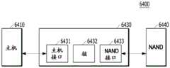
图11是示意性地图示根据实施例的包括存储器系统的数据处理系统的另一示例的图。图11示意性地图示了可以应用存储器系统的嵌入式多媒体卡(eMMC)6400。FIG. 11 is a diagram schematically illustrating another example of a data processing system including a memory system according to an embodiment. Figure 11 schematically illustrates an embedded multimedia card (eMMC) 6400 to which the memory system may be applied.

参考图11,eMMC 6400可以包括控制器6430和由一个或多个NAND闪存实现的存储器装置6440。控制器6430可以对应于图1的存储器系统110中的控制器130,并且存储器装置6440可以对应于图1的存储器系统110中的存储器装置150。Referring to FIG. 11, theeMMC 6400 may include acontroller 6430 and amemory device 6440 implemented by one or more NAND flash memories.Controller 6430 may correspond tocontroller 130 inmemory system 110 of FIG. 1 , andmemory device 6440 may correspond tomemory device 150 inmemory system 110 of FIG. 1 .

更具体地,控制器6430可以通过多个信道连接到存储器装置6440。控制器6430可以包括一个或多个核6432、主机接口(I/F)6431和存储器接口(例如,NAND接口(I/F))6433。More specifically, thecontroller 6430 may be connected to thememory device 6440 through multiple channels.Controller 6430 may include one ormore cores 6432 , host interface (I/F) 6431 , and memory interface (eg, NAND interface (I/F)) 6433 .

核6432可以控制eMMC 6400的整体操作,主机接口6431可以在控制器6430和主机6410之间提供接口功能,并且NAND接口6433可以在存储器装置6440和控制器6430之间提供接口功能。例如,主机接口6431可以用作并行接口(例如,参考图1描述的MMC接口)。此外,主机接口6431可以用作串行接口(例如,超高速(UHS)-I和UHS-II接口)。Thecore 6432 can control the overall operation of theeMMC 6400, thehost interface 6431 can provide interface functions between thecontroller 6430 and thehost 6410, and theNAND interface 6433 can provide interface functions between thememory device 6440 and thecontroller 6430. For example, thehost interface 6431 may function as a parallel interface (eg, the MMC interface described with reference to FIG. 1). In addition, thehost interface 6431 can be used as a serial interface (eg, Ultra High Speed (UHS)-I and UHS-II interfaces).

图12至图15是示意性图示根据一个或多个实施例的包括存储器系统的数据处理系统的其他示例的图。图12至图15示意性地图示了可以应用存储器系统的通用闪存(UFS)系统。12-15 are diagrams schematically illustrating other examples of data processing systems including a memory system in accordance with one or more embodiments. 12 to 15 schematically illustrate a Universal Flash Memory (UFS) system to which the memory system may be applied.

参考图12至图15,UFS系统6500、6600、6700和6800可以分别包括主机6510、6610、6710和6810、UFS装置6520、6620、6720、和6820以及UFS卡6530、6630、6730和6830。主机6510、6610、6710和6810可以用作有线和/或无线电子装置或者特别是移动电子装置的应用处理器,UFS装置6520、6620、6720和6820可以用作嵌入式UFS装置。UFS卡6530、6630、6730和6830可以用作外部嵌入式UFS装置或可移除UFS卡。12 to 15,UFS systems 6500, 6600, 6700, and 6800 may includehosts 6510, 6610, 6710, and 6810,UFS devices 6520, 6620, 6720, and 6820, andUFS cards 6530, 6630, 6730, and 6830, respectively. Thehosts 6510, 6610, 6710 and 6810 can act as wired and/or wireless electronic devices or application processors in particular for mobile electronic devices, and theUFS devices 6520, 6620, 6720 and 6820 can act as embedded UFS devices.UFS cards 6530, 6630, 6730 and 6830 can be used as external embedded UFS devices or removable UFS cards.

相应UFS系统6500、6600、6700和6800中的主机6510、6610、6710和6810、UFS装置6520、6620、6720和6820以及UFS卡6530、6630、6730和6830可以通过UFS协议与外部装置(例如,有线和/或无线电子装置或者特别是移动电子装置)通信。UFS装置6520、6620、6720和6820以及UFS卡6530、6630、6730和6830可以由图1所示的存储器系统110来体现。例如,在UFS系统6500、6600、6700和6800中,UFS装置6520、6620、6720和6820可以以参考图9至图11所描述的数据处理系统6200、SSD 6300或eMMC 6400的形式来体现,并且UFS卡6530、6630、6730和6830可以以参考图8描述的存储器卡系统6100的形式来体现。Hosts 6510, 6610, 6710, and 6810,UFS devices 6520, 6620, 6720, and 6820, andUFS cards 6530, 6630, 6730, and 6830 in correspondingUFS systems 6500, 6600, 6700, and 6800 can communicate with external devices (eg, UFS wired and/or wireless electronic devices or especially mobile electronic devices) communication.UFS devices 6520 , 6620 , 6720 and 6820 andUFS cards 6530 , 6630 , 6730 and 6830 may be embodied bymemory system 110 shown in FIG. 1 . For example, inUFS systems 6500, 6600, 6700, and 6800,UFS devices 6520, 6620, 6720, and 6820 may be embodied in the form ofdata processing systems 6200,SSD 6300, oreMMC 6400 described with reference to FIGS. 9-11, andUFS cards 6530 , 6630 , 6730 and 6830 may be embodied in the form ofmemory card system 6100 described with reference to FIG. 8 .

此外,在UFS系统6500、6600、6700和6800中,主机6510、6610、6710和6810、UFS装置6520、6620、6720和6820以及UFS卡6530、6630、6730和6830可以通过UFS接口(例如,MIPI(移动行业处理器接口)中的MIPI M-PHY和MIPI UniPro(统一协议))彼此通信。此外,UFS装置6520、6620、6720和6820以及UFS卡6530、6630、6730和6830可以通过除了UFS协议以外的各种协议(例如,通用存储总线(USB)闪存驱动器(UFD)、多媒体卡(MMC)、安全数字(SD)、小型SD和微型SD)彼此通信。In addition, inUFS systems 6500, 6600, 6700, and 6800, hosts 6510, 6610, 6710, and 6810,UFS devices 6520, 6620, 6720, and 6820, andUFS cards 6530, 6630, 6730, and 6830 can use UFS interfaces (eg, MIPI (Mobile Industry Processor Interface) MIPI M-PHY and MIPI UniPro (Unified Protocol)) communicate with each other. In addition, theUFS devices 6520, 6620, 6720, and 6820 and theUFS cards 6530, 6630, 6730, and 6830 can pass various protocols other than the UFS protocol (eg, Universal Storage Bus (USB) Flash Drive (UFD), Multimedia Card (MMC) ), Secure Digital (SD), Mini SD, and Micro SD) communicate with each other.

在图12中所示的UFS系统6500中,主机6510、UFS装置6520和UFS卡6530中的每一个可以包括UniPro。主机6510可以执行切换操作以便与UFS装置6520和UFS卡6530通信。特别地,主机6510可以通过链路层切换(例如,以UniPro的L3切换)与UFS装置6520或UFS卡6530通信。UFS装置6520和UFS卡6530可以通过主机6510的UniPro处的链路层切换彼此通信。在图12中,通过示例图示了一个UFS装置6520和一个UFS卡6530连接到主机6510的配置。然而,多个UFS装置和UFS卡可以并联或以星形的形式连接到主机6510,并且多个UFS卡可以并联或以星形的形式连接到UFS装置6520,或者以串联或以链的形式连接到UFS装置6520。In theUFS system 6500 shown in FIG. 12, each of thehost 6510, theUFS device 6520, and theUFS card 6530 may include a UniPro. Thehost 6510 may perform switching operations to communicate with theUFS device 6520 and theUFS card 6530. In particular, thehost 6510 can communicate with theUFS device 6520 or theUFS card 6530 through link layer switching (eg, with UniPro's L3 switching). TheUFS device 6520 and theUFS card 6530 can communicate with each other through link layer switching at the UniPro of thehost 6510. In FIG. 12, a configuration in which oneUFS device 6520 and oneUFS card 6530 are connected to thehost 6510 is illustrated by way of example. However, multiple UFS devices and UFS cards can be connected to thehost 6510 in parallel or in a star, and multiple UFS cards can be connected in parallel or in a star to theUFS device 6520, or in series or in a chain toUFS Unit 6520.

在图13所示的UFS系统6600中,主机6610、UFS装置6620和UFS卡6630中的每一个可以包括UniPro,并且主机6610可以通过执行切换操作的切换模块6640(例如,通过以UniPro执行链路层切换(例如,L3切换)的切换模块6640)与UFS装置6620或UFS卡6630通信。UFS装置6620和UFS卡6630可以通过UniPro处的切换模块6640的链路层切换来彼此通信。在图13中,通过示例的方式图示了一个UFS装置6620和一个UFS卡6630连接到切换模块6640的配置。然而,多个UFS装置和UFS卡可以并联或以星形的形式连接到切换模块6640,并且多个UFS卡可以串联或以链的形式连接到UFS装置6620。In theUFS system 6600 shown in FIG. 13, each of thehost 6610, theUFS device 6620, and theUFS card 6630 may include a UniPro, and thehost 6610 may pass aswitching module 6640 that performs a switching operation (eg, by performing a link with UniPro) Theswitching module 6640 of layer switching (eg, L3 switching) communicates with theUFS device 6620 or theUFS card 6630.UFS device 6620 andUFS card 6630 can communicate with each other through link layer switching ofswitching module 6640 at UniPro. In FIG. 13, a configuration in which oneUFS device 6620 and oneUFS card 6630 are connected to theswitching module 6640 is illustrated by way of example. However, multiple UFS devices and UFS cards can be connected to theswitching module 6640 in parallel or in a star, and multiple UFS cards can be connected to theUFS devices 6620 in series or in a chain.

在图14所示的UFS系统6700中,主机6710、UFS装置6720和UFS卡6730中的每一个可以包括UniPro。主机6710可以通过执行切换操作的切换模块6740(例如,通过以UniPro执行链路层切换(例如,L3切换)的切换模块6740)与UFS装置6720或UFS卡6730通信。UFS装置6720和UFS卡6730可以通过UniPro处的切换模块6740的链路层切换来彼此通信,并且切换模块6740可以与UFS装置6720作为一个模块集成在UFS装置6720内部或外部。在图14中,通过示例的方式图示了一个UFS装置6720和一个UFS卡6730连接到切换模块6740的配置。然而,各自包括切换模块6740和UFS装置6720的多个模块可以并联或以星形的形式连接到主机6710,或者串联或以链的形式彼此连接。此外,多个UFS卡可以并联或以星形的形式连接到UFS装置6720。In theUFS system 6700 shown in FIG. 14, each of thehost 6710, theUFS device 6720, and theUFS card 6730 may include a UniPro.Host 6710 may communicate withUFS device 6720 orUFS card 6730 throughswitch module 6740 that performs switching operations (eg, throughswitch module 6740 that performs link layer switching (eg, L3 switching) with UniPro). TheUFS device 6720 and theUFS card 6730 can communicate with each other through link layer switching of theswitching module 6740 at UniPro, and theswitching module 6740 can be integrated with theUFS device 6720 as a module inside or outside theUFS device 6720. In FIG. 14, a configuration in which oneUFS device 6720 and oneUFS card 6730 are connected to theswitching module 6740 is illustrated by way of example. However, multiple modules, each including theswitching module 6740 and theUFS device 6720, may be connected to thehost 6710 in parallel or in a star, or connected to each other in series or in a chain. Additionally, multiple UFS cards can be connected to theUFS unit 6720 in parallel or in a star.

在图15所示的UFS系统6800中,主机6810、UFS装置6820和UFS卡6830中的每一个可以包括M-PHY和UniPro。UFS装置6820可以执行切换操作,以便与主机6810和UFS卡6830通信。特别地,UFS装置6820可以通过用于与主机6810通信的M-PHY和UniPro模块和用于与UFS卡6830通信的M-PHY和UniPro模块之间的切换操作(例如,通过目标标识符(ID)切换操作)与主机6810或UFS卡6830通信。主机6810和UFS卡6830可以通过在UFS装置6820的M-PHY和UniPro模块之间的目标ID切换来彼此通信。在图15中,通过示例的方式图示了一个UFS装置6820连接到主机6810并且一个UFS卡6830连接到UFS装置6820的配置。但是,多个UFS装置可以并联或以星形的形式连接到主机6810,或者串联或以链的形式连接到主机6810,并且多个UFS卡可以并联或以星形的形式连接到UFS装置6820,或者串联或以链的形式连接到UFS装置6820。In theUFS system 6800 shown in FIG. 15, each of thehost 6810, theUFS device 6820, and theUFS card 6830 may include M-PHY and UniPro.UFS device 6820 may perform switching operations to communicate withhost 6810 andUFS card 6830. In particular, theUFS device 6820 may operate through switching between the M-PHY and UniPro modules for communicating with thehost 6810 and the M-PHY and UniPro modules for communicating with the UFS card 6830 (eg, through a target identifier (ID) ) switch operation) communicate with thehost 6810 or theUFS card 6830. Thehost 6810 and theUFS card 6830 can communicate with each other through target ID switching between the M-PHY of theUFS device 6820 and the UniPro module. In FIG. 15, a configuration in which oneUFS device 6820 is connected to thehost 6810 and oneUFS card 6830 is connected to theUFS device 6820 is illustrated by way of example. However, multiple UFS devices can be connected to thehost 6810 in parallel or in a star, or connected in series or in a chain to thehost 6810, and multiple UFS cards can be connected in parallel or in a star to theUFS device 6820, Either in series or in a chain to theUFS unit 6820.

图16是示意性地图示根据实施例的包括存储器系统的数据处理系统的另一示例的图。图16是示意性地图示可以应用存储器系统的用户系统6900的图。FIG. 16 is a diagram schematically illustrating another example of a data processing system including a memory system according to an embodiment. FIG. 16 is a diagram schematically illustrating auser system 6900 to which the memory system may be applied.

参考图16,用户系统6900可以包括用户接口6910、存储器模块6920、应用处理器6930、网络模块6940和存储模块6950。Referring to FIG. 16 , theuser system 6900 may include auser interface 6910 , amemory module 6920 , anapplication processor 6930 , anetwork module 6940 and astorage module 6950 .

更具体地,应用处理器6930可以驱动用户系统6900中包括的部件(例如,操作系统OS)并且包括对用户系统6900中包括的部件进行控制的控制器、接口和图形引擎。应用处理器6930可以被设置为片上系统(SoC)。More specifically, theapplication processor 6930 may drive components included in the user system 6900 (eg, an operating system OS) and include a controller, an interface, and a graphics engine that control the components included in theuser system 6900 . Theapplication processor 6930 may be provided as a system on a chip (SoC).

存储器模块6920可以用作用户系统6900的主存储器、工作存储器、缓冲存储器或高速缓存存储器。存储器模块6920可以包括易失性随机存取存储器(RAM)(诸如动态RAM(DRAM)、同步DRAM(SDRAM)、双倍数据速率(DDR)SDRAM、DDR2 SDRAM、DDR3 SDRAM、LPDDRSDARM、LPDDR2 SDRAM或LPDDR3 SDRAM)或非易失性RAM(诸如相变RAM(PRAM)、电阻式RAM(ReRAM)、磁阻式RAM(MRAM)或铁电式RAM(FRAM))。例如,可以基于堆叠封装(PoP)来封装和安装应用处理器6930和存储器模块6920。Thememory module 6920 may function as main memory, working memory, buffer memory, or cache memory of theuser system 6900. Thememory module 6920 may include volatile random access memory (RAM) such as dynamic RAM (DRAM), synchronous DRAM (SDRAM), double data rate (DDR) SDRAM, DDR2 SDRAM, DDR3 SDRAM, LPDDRSDARM, LPDDR2 SDRAM, or LPDDR3 SDRAM) or non-volatile RAM such as phase change RAM (PRAM), resistive RAM (ReRAM), magnetoresistive RAM (MRAM) or ferroelectric RAM (FRAM). For example, theapplication processor 6930 and thememory module 6920 may be packaged and mounted on a package-on-package (PoP) basis.

网络模块6940可以与外部装置通信。例如,网络模块6940不仅可以支持有线通信,而且可以支持各种无线通信协议(诸如码分多址(CDMA)、全球移动通信系统(GSM)、宽带CDMA(WCDMA)、CDMA-2000、时分多址(TDMA)、长期演进(LTE)、全球微波接入互通(Wimax)、无线局域网(WLAN)、超宽带(UWB)、蓝牙、无线显示(WI-DI)),从而与有线/无线电子装置或特别是移动电子装置进行通信。因此,根据本发明的实施例,存储器系统和数据处理系统可以应用于有线/无线电子装置。网络模块6940可以被包括在应用处理器6930中。Thenetwork module 6940 can communicate with external devices. For example, thenetwork module 6940 can support not only wired communication but also various wireless communication protocols such as Code Division Multiple Access (CDMA), Global System for Mobile Communications (GSM), Wideband CDMA (WCDMA), CDMA-2000, Time Division Multiple Access (TDMA), Long Term Evolution (LTE), Worldwide Interoperability for Microwave Access (Wimax), Wireless Local Area Network (WLAN), Ultra-Wideband (UWB), Bluetooth, Wireless Display (WI-DI)), so as to communicate with wired/wireless electronic devices or Especially mobile electronic devices communicate. Therefore, according to the embodiments of the present invention, the memory system and the data processing system may be applied to wired/wireless electronic devices. Thenetwork module 6940 may be included in theapplication processor 6930.

存储模块6950可以存储数据(例如,从应用处理器6930接收的数据),然后可以将所存储的数据传输到应用处理器6930。存储模块6950可以由诸如相变RAM(PRAM)、磁性RAM(MRAM)、电阻式RAM(ReRAM)、NAND闪存、NOR闪存和3D NAND闪存的非易失性半导体存储器装置来实现,并且被设置为用户系统6900的可移除存储介质(诸如存储器卡或外部驱动器)。存储模块6950可以对应于参考图1描述的存储器系统110。此外,存储模块6950可以被实现为以上参考图10至图15描述的SSD、eMMC和UFS。Thestorage module 6950 can store data (eg, data received from the application processor 6930 ), which can then be transmitted to theapplication processor 6930 . Thememory module 6950 may be implemented by a non-volatile semiconductor memory device such as phase-change RAM (PRAM), magnetic RAM (MRAM), resistive RAM (ReRAM), NAND flash memory, NOR flash memory, and 3D NAND flash memory, and is configured to A removable storage medium (such as a memory card or external drive) of theuser system 6900. Thestorage module 6950 may correspond to thememory system 110 described with reference to FIG. 1 . Also, thestorage module 6950 may be implemented as the SSD, eMMC, and UFS described above with reference to FIGS. 10 to 15 .

用户接口6910可以包括用于向应用处理器6930输入数据或命令或向外部装置输出数据的接口。例如,用户接口6910可以包括用户输入接口(诸如键盘、小键盘、按钮、触摸面板、触摸屏、触摸板、触摸球、相机、麦克风、陀螺仪传感器、振动传感器和压电元件)以及用户输出接口(诸如液晶显示器(LCD)、有机发光二极管(OLED)显示装置、有源矩阵OLED(AMOLED)显示装置、LED、扬声器和电机)。Theuser interface 6910 may include an interface for inputting data or commands to theapplication processor 6930 or outputting data to an external device. For example,user interface 6910 may include user input interfaces (such as keyboards, keypads, buttons, touch panels, touch screens, touch pads, touch balls, cameras, microphones, gyroscope sensors, vibration sensors, and piezoelectric elements) and user output interfaces ( Such as liquid crystal display (LCD), organic light emitting diode (OLED) display device, active matrix OLED (AMOLED) display device, LED, speaker and motor).

此外,当图1的存储器系统110应用于用户系统6900的移动电子装置时,应用处理器6930可以控制移动电子装置的整体操作,并且网络模块6940可以用作用于控制与外部装置的有线和/或无线通信的通信模块。用户接口6910可以在移动电子装置的显示/触摸模块上显示由应用处理器6930处理的数据或者支持从触摸面板接收数据的功能。Furthermore, when thememory system 110 of FIG. 1 is applied to the mobile electronic device of theuser system 6900, theapplication processor 6930 may control the overall operation of the mobile electronic device, and thenetwork module 6940 may be used for controlling wired and/or wired and/or external devices Communication module for wireless communication. Theuser interface 6910 may display data processed by theapplication processor 6930 on the display/touch module of the mobile electronic device or support the function of receiving data from the touch panel.

根据本发明实施例的存储器系统可以有效地处理针对大容量映射数据的取消映射命令,从而提高了存储器系统的取消映射性能。The memory system according to the embodiment of the present invention can efficiently process the unmap command for large-capacity mapped data, thereby improving the unmap performance of the memory system.

虽然已关于特定实施例图示和描述了本发明,但是根据本公开,对于本领域技术人员而言显而易见的是,在不脱离如所附权利要求限定的本发明的精神和范围的情况下,可以进行各种改变和修改。While the invention has been illustrated and described with respect to specific embodiments, it will be apparent to those skilled in the art from this disclosure that, without departing from the spirit and scope of the invention as defined by the appended claims, Various changes and modifications can be made.

Claims (20)

Translated fromChinese
1.一种存储器系统,包括:1. A memory system comprising:存储器装置,适于存储与针对取消映射命令的目标逻辑地址相关联的第一映射信息和第二映射信息;以及a memory device adapted to store first mapping information and second mapping information associated with a target logical address for an unmap command; and控制器,适于从所述存储器装置加载所述第一映射信息和所述第二映射信息,将与所述目标逻辑地址相对应的目标映射数据的大小与阈值进行比较,基于所述比较的结果来将与包括所述目标逻辑地址中的一个或多个的多个目标逻辑组分别映射的多个映射段分类到多个区域,并且对所述多个区域中包括的所述映射段中的每一个执行取消映射操作,a controller adapted to load the first mapping information and the second mapping information from the memory device, compare the size of the target mapping data corresponding to the target logical address with a threshold, and based on the comparison As a result, a plurality of mapped segments respectively mapped with a plurality of target logical groups including one or more of the target logical addresses are classified into a plurality of regions, and the mapping segments included in the plurality of regions are classified into a plurality of regions. each performs an unmap operation,其中所述第一映射信息包括关于所述多个映射段与所述多个目标逻辑组之间的映射关系的信息,并且所述第二映射信息包括关于所述目标逻辑地址与对应物理地址之间的映射关系的信息。The first mapping information includes information about the mapping relationship between the plurality of mapping segments and the plurality of target logical groups, and the second mapping information includes information about the relationship between the target logical address and the corresponding physical address. information about the mapping relationship between them.2.根据权利要求1所述的存储器系统,其中所述控制器包括:2. The memory system of claim 1, wherein the controller comprises:存储器,适于存储所述第一映射信息和所述第二映射信息;a memory adapted to store the first mapping information and the second mapping information;处理器,适于将所述第一映射信息和所述第二映射信息从所述存储器装置加载到所述存储器中;以及a processor adapted to load the first mapping information and the second mapping information from the memory device into the memory; and取消映射管理器,适于将所述目标映射数据的所述大小与所述阈值进行比较,基于所述比较的结果来将所述多个映射段分类到所述多个区域,并且对所述多个区域中的所述映射段中的每一个的所述第一映射信息执行所述取消映射操作。an unmap manager adapted to compare the size of the target map data to the threshold value, classify the plurality of mapped segments into the plurality of regions based on a result of the comparison, and The unmap operation is performed by the first mapping information of each of the mapped segments in the plurality of regions.3.根据权利要求2所述的存储器系统,其中当所述目标映射数据的所述大小大于或等于所述阈值时,所述取消映射管理器将与其中所述多个逻辑地址中的仅一些是所述目标逻辑地址的第一逻辑组映射的映射段分类到第一区域和第三区域,并且将与其中所有逻辑地址是所述目标逻辑地址的第二逻辑组映射的映射段分类到第二区域。3. The memory system of claim 2, wherein when the size of the target mapped data is greater than or equal to the threshold, the unmap manager will interact with only some of the plurality of logical addresses therein The mapped segment that is the first logical group mapping of the target logical address is classified into the first region and the third region, and the mapped segment mapped to the second logical group in which all logical addresses are the target logical address is classified into the first region. Second area.4.根据权利要求3所述的存储器系统,其中所述取消映射管理器将与包括所述第一逻辑组中的所述目标逻辑地址的起始逻辑地址的逻辑组映射的映射段分类到所述第一区域,并且将与包括所述第一逻辑组中的所述目标逻辑地址的最后逻辑地址的逻辑组映射的映射段分类到所述第三区域。4. The memory system of claim 3, wherein the unmap manager classifies a mapped segment mapped with a logical group that includes a starting logical address of the target logical address in the first logical group to the the first area, and the mapped segment mapped with the logical group including the last logical address of the target logical address in the first logical group is classified into the third area.5.根据权利要求3所述的存储器系统,其中所述取消映射管理器对所述第二区域中的所述映射段中的每一个的所述第一映射信息执行第一取消映射操作,并且对与所述第一区域的相应映射段和所述第三区域的相应映射段映射的逻辑组的所述目标逻辑地址的所述第二映射信息执行第二取消映射操作。5. The memory system of claim 3, wherein the unmap manager performs a first unmap operation on the first mapping information for each of the mapped segments in the second region, and A second unmap operation is performed on the second mapping information of the target logical address of the logical group mapped with the corresponding mapped segment of the first region and the corresponding mapped segment of the third region.6.根据权利要求5所述的存储器系统,其中在所述第一取消映射操作被执行之后,所述处理器将所述第一映射信息存储在所述存储器装置中。6. The memory system of claim 5, wherein the processor stores the first mapping information in the memory device after the first unmap operation is performed.7.根据权利要求5所述的存储器系统,其中在所述第二取消映射操作被执行之后,所述处理器将所述第二映射信息存储在所述存储器装置中。7. The memory system of claim 5, wherein the processor stores the second mapping information in the memory device after the second unmap operation is performed.8.根据权利要求2所述的存储器系统,其中当所述目标映射数据的整体大小小于所述阈值时,所述取消映射管理器对所述目标逻辑地址的所述第二映射信息执行第三取消映射操作。8. The memory system of claim 2, wherein when the overall size of the target mapping data is less than the threshold, the unmap manager performs a third mapping on the second mapping information of the target logical address Unmap operation.9.根据权利要求8所述的存储器系统,其中在所述第三取消映射操作被执行之后,所述处理器将所述第二映射信息存储在所述存储器装置中。9. The memory system of claim 8, wherein the processor stores the second mapping information in the memory device after the third unmap operation is performed.10.根据权利要求2所述的存储器系统,其中所述存储器存储其中存储有所述第一映射信息的第一表和其中存储有所述第二映射信息的第二表。10. The memory system of claim 2, wherein the memory stores a first table in which the first mapping information is stored and a second table in which the second mapping information is stored.11.一种存储器系统的操作方法,所述操作方法包括:11. A method of operating a memory system, the operating method comprising:接收取消映射命令;receive an unmap command;从存储器装置加载与针对所述取消映射命令的目标逻辑地址相关联的第一映射信息和第二映射信息,并且将所述第一映射信息和所述第二映射信息存储在存储器中;Loading first mapping information and second mapping information associated with the target logical address for the unmap command from a memory device, and storing the first mapping information and the second mapping information in memory;将对应于所述目标逻辑地址的目标映射数据的大小与阈值进行比较;comparing the size of the target map data corresponding to the target logical address with a threshold;基于所述比较的结果,将与包括所述目标逻辑地址中的一个或多个的多个目标逻辑组分别映射的多个映射段分类到多个区域;以及classifying a plurality of mapped segments respectively mapped with a plurality of target logical groups including one or more of the target logical addresses into a plurality of regions based on a result of the comparison; and对所述多个区域中的任一个中包括的每个映射段执行取消映射操作,performing an unmap operation on each mapped segment included in any of the plurality of regions,其中所述第一映射信息包括关于所述多个映射段与所述多个目标逻辑组之间的映射关系的信息,并且所述第二映射信息包括关于所述目标逻辑地址与对应物理地址之间的映射关系的信息。The first mapping information includes information about the mapping relationship between the plurality of mapping segments and the plurality of target logical groups, and the second mapping information includes information about the relationship between the target logical address and the corresponding physical address. information about the mapping relationship between them.12.根据权利要求11所述的操作方法,其中将所述多个映射段分类到所述多个区域包括:当所述目标映射数据的所述大小大于或等于所述阈值时,将与所述目标逻辑组映射的所述多个映射段分类到所述多个区域。12. The operating method of claim 11, wherein classifying the plurality of map segments into the plurality of regions comprises: when the size of the target map data is greater than or equal to the threshold, The plurality of mapped segments of the target logical group map are classified into the plurality of regions.13.根据权利要求12所述的操作方法,其中将所述多个映射段分类到所述多个区域包括:在所述多个映射段之中,将与其中多个逻辑地址中的仅一些是所述目标逻辑地址的第一逻辑组映射的映射段分类到第一区域和第三区域,并且将与其中所有逻辑地址是所述目标逻辑地址的第二逻辑组映射的映射段分类到第二区域。13. The operating method of claim 12, wherein classifying the plurality of mapped segments into the plurality of regions comprises: among the plurality of mapped segments, comparing only some of the plurality of logical addresses with The mapped segment that is the first logical group mapping of the target logical address is classified into the first region and the third region, and the mapped segment mapped to the second logical group in which all logical addresses are the target logical address is classified into the first region. Second area.14.根据权利要求13所述的操作方法,其中将所述多个映射段分类到所述多个区域包括:14. The method of operation of claim 13, wherein classifying the plurality of mapped segments into the plurality of regions comprises:将与包括所述第一逻辑组中的所述目标逻辑地址的起始逻辑地址的逻辑组映射的映射段分类到所述第一区域,以及classifying into the first region a mapped segment mapped with a logical group that includes a starting logical address of the target logical address in the first logical group, and将与包括所述第一逻辑组中的所述目标逻辑地址的最后逻辑地址的逻辑组映射的映射段分类到所述第三区域。A mapped segment mapped with a logical group including the last logical address of the target logical address in the first logical group is classified into the third region.15.根据权利要求13所述的操作方法,其中执行所述取消映射操作包括:15. The operating method of claim 13, wherein performing the unmap operation comprises:对所述第二区域中的所述映射段中的每一个的所述第一映射信息进行第一取消映射操作;以及performing a first unmap operation on the first mapping information for each of the mapped segments in the second region; and对与所述第一区域的相应映射段和所述第三区域的相应映射段映射的逻辑组中的所述目标逻辑地址的所述第二映射信息执行第二取消映射操作。A second unmap operation is performed on the second mapping information of the target logical address in the logical group mapped with the corresponding mapped segment of the first region and the corresponding mapped segment of the third region.16.根据权利要求15所述的操作方法,进一步包括:在执行所述第一取消映射操作之后,将所述第一映射信息存储在所述存储器装置中。16. The operating method of claim 15, further comprising storing the first mapping information in the memory device after performing the first unmapping operation.17.根据权利要求15所述的操作方法,进一步包括:在执行所述第二取消映射操作之后,将所述第二映射信息存储在所述存储器装置中。17. The operating method of claim 15, further comprising storing the second mapping information in the memory device after performing the second unmap operation.18.根据权利要求11所述的操作方法,其中执行所述取消映射操作包括:当所述目标映射数据的所述大小小于所述阈值时,对所述目标逻辑地址的所述第二映射信息执行第三取消映射操作。18. The operating method of claim 11, wherein performing the unmapping operation comprises: when the size of the target mapping data is less than the threshold, mapping the second mapping information of the target logical address A third unmap operation is performed.19.根据权利要求18所述的操作方法,进一步包括:在执行所述第三取消映射操作之后,将所述第二映射信息存储在所述存储器装置中。19. The operating method of claim 18, further comprising storing the second mapping information in the memory device after performing the third unmap operation.20.一种存储器系统,包括:20. A memory system comprising:存储器装置,适于存储第一映射信息和第二映射信息,所述第一映射信息包括关于多个映射段与多个逻辑组之间的映射的信息,每个逻辑组包括一个或多个逻辑地址,并且所述第二映射信息包括关于多个逻辑地址与多个物理地址之间的映射的信息;以及a memory device adapted to store first mapping information and second mapping information, the first mapping information including information regarding mappings between a plurality of mapped segments and a plurality of logical groups, each logical group including one or more logical groups addresses, and the second mapping information includes information about mappings between the plurality of logical addresses and the plurality of physical addresses; and控制器,包括存储器,适于:Controller, including memory, suitable for:将与取消映射命令相关联的所述第一映射信息和所述第二映射信息从所述存储器装置加载到所述存储器中;loading the first mapping information and the second mapping information associated with an unmap command from the memory device into the memory;将包括第一映射段、最后映射段和其余映射段的所述多个映射段划分到包括所述第一映射段的第一组、包括所述其余映射段的第二组和包括所述最后映射段的第三组;以及dividing the plurality of mapped segments including the first mapped segment, the last mapped segment, and the remaining mapped segments into a first group including the first mapped segment, a second group including the remaining mapped segment, and a group including the last mapped segment the third group of mapped segments; and将针对所述第一组和所述第三组的所述第二映射信息取消映射,并且将针对所述第二组的所述第一映射信息取消映射。The second mapping information for the first group and the third group is unmapped, and the first mapping information for the second group is unmapped.
CN201911213480.9A2018-12-172019-12-02 Memory system and method of operation thereofActiveCN111324552B (en)

Applications Claiming Priority (2)

Application NumberPriority DateFiling DateTitle
KR10-2018-01632812018-12-17
KR1020180163281AKR102761223B1 (en)2018-12-172018-12-17Memory system and operating method thereof

Publications (2)

Publication NumberPublication Date
CN111324552Atrue CN111324552A (en)2020-06-23
CN111324552B CN111324552B (en)2023-03-03

Family

ID=71072566

Family Applications (1)

Application NumberTitlePriority DateFiling Date
CN201911213480.9AActiveCN111324552B (en)2018-12-172019-12-02 Memory system and method of operation thereof

Country Status (3)

CountryLink
US (1)US11016881B2 (en)
KR (1)KR102761223B1 (en)
CN (1)CN111324552B (en)

Cited By (3)

* Cited by examiner, † Cited by third party
Publication numberPriority datePublication dateAssigneeTitle
CN117234959A (en)*2023-08-292023-12-15中电云计算技术有限公司Data processing method, device, equipment and storage medium
CN117891416A (en)*2024-03-182024-04-16厦门大学Unmapping operation optimization method and device based on SCSI protocol and readable medium
WO2024243855A1 (en)*2023-05-312024-12-05长江存储科技有限责任公司Memory system, operation method therefor, storage medium and memory controller

Families Citing this family (4)

* Cited by examiner, † Cited by third party
Publication numberPriority datePublication dateAssigneeTitle
US11733918B2 (en)*2020-07-282023-08-22Samsung Electronics Co., Ltd.Systems and methods for processing commands for storage devices
US11755490B2 (en)*2020-12-152023-09-12Micron Technology, Inc.Unmap operation techniques
US20230013048A1 (en)*2021-07-162023-01-19International Business Machines CorporationHandling partition data
CN115904226A (en)2022-10-102023-04-04阿里巴巴(中国)有限公司Solid state drive, apparatus and method of operating solid state drive

Citations (6)

* Cited by examiner, † Cited by third party
Publication numberPriority datePublication dateAssigneeTitle
US4758951A (en)*1985-04-091988-07-19Tektronix, Inc.Method for translating virtual addresses into real addresses
US20120060012A1 (en)*2010-09-032012-03-08International Business Machines CorporationManagement of low-paging space conditions in an operating system
WO2015048140A1 (en)*2013-09-242015-04-02Intelligent Intellectual Property Holdings 2 LlcSystems and methods for storage collision management
CN107220184A (en)*2017-05-102017-09-29杭州宏杉科技股份有限公司The management method and device of a kind of LUN memory cell
CN108073470A (en)*2016-11-072018-05-25三星电子株式会社Perform the storage system and its control method of the error correction of address mapping table
CN108694128A (en)*2017-04-102018-10-23桑迪士克科技有限责任公司The newer folding operation in single address is used in storage system

Family Cites Families (12)

* Cited by examiner, † Cited by third party
Publication numberPriority datePublication dateAssigneeTitle
US7552308B2 (en)2006-04-042009-06-23International Business Machines CorporationMethod and apparatus for temporary mapping of executable program segments
US9069657B2 (en)2011-12-122015-06-30Apple Inc.LBA bitmap usage
US9323667B2 (en)2012-04-122016-04-26Violin Memory Inc.System and method for managing trim operations in a flash memory system using mapping tables and block status tables
US9558125B2 (en)*2014-10-272017-01-31Sandisk Technologies LlcProcessing of un-map commands to enhance performance and endurance of a storage device
JP2018116329A (en)*2017-01-162018-07-26富士通株式会社Storage control apparatus and storage control program
US10459636B2 (en)*2017-03-242019-10-29Sandisk Technologies LlcSystem and method for managing data in non-volatile memory systems having multiple mapping layers
US11182106B2 (en)*2018-03-212021-11-23Arm LimitedRefresh circuit for use with integrated circuits
KR20200019430A (en)*2018-08-142020-02-24에스케이하이닉스 주식회사Controller and operating method thereof
US10909030B2 (en)*2018-09-112021-02-02Toshiba Memory CorporationEnhanced trim command support for solid state drives
KR102679967B1 (en)*2018-09-122024-07-02에스케이하이닉스 주식회사Apparatus and method for managing valid data in memory system
KR102711044B1 (en)*2018-09-202024-09-27에스케이하이닉스 주식회사Apparatus and method for checking valid data in memory system
US10901649B2 (en)*2019-01-232021-01-26Vmware, Inc.Storage reclamation for distributed storage systems

Patent Citations (6)

* Cited by examiner, † Cited by third party
Publication numberPriority datePublication dateAssigneeTitle
US4758951A (en)*1985-04-091988-07-19Tektronix, Inc.Method for translating virtual addresses into real addresses
US20120060012A1 (en)*2010-09-032012-03-08International Business Machines CorporationManagement of low-paging space conditions in an operating system
WO2015048140A1 (en)*2013-09-242015-04-02Intelligent Intellectual Property Holdings 2 LlcSystems and methods for storage collision management
CN108073470A (en)*2016-11-072018-05-25三星电子株式会社Perform the storage system and its control method of the error correction of address mapping table
CN108694128A (en)*2017-04-102018-10-23桑迪士克科技有限责任公司The newer folding operation in single address is used in storage system
CN107220184A (en)*2017-05-102017-09-29杭州宏杉科技股份有限公司The management method and device of a kind of LUN memory cell

Non-Patent Citations (2)

* Cited by examiner, † Cited by third party
Title
I-TING ANGELINA LEE .ETC: "Using Memory Mapping to Support Cactus Stacks in Work-Stealing Runtime Systems", 《2010 19TH INTERNATIONAL CONFERENCE ON PARALLEL ARCHITECTURES AND COMPILATION TECHNIQUES(PACT)》*
曹非: "片上多核处理器共享末级缓存动静结合地址映射机制", 《计算机科学》*

Cited By (5)

* Cited by examiner, † Cited by third party
Publication numberPriority datePublication dateAssigneeTitle
WO2024243855A1 (en)*2023-05-312024-12-05长江存储科技有限责任公司Memory system, operation method therefor, storage medium and memory controller
US12282435B2 (en)2023-05-312025-04-22Yangtze Memory Technologies Co., Ltd.Memory system and method of operating thereof, storage medium and memory controller
CN117234959A (en)*2023-08-292023-12-15中电云计算技术有限公司Data processing method, device, equipment and storage medium
CN117891416A (en)*2024-03-182024-04-16厦门大学Unmapping operation optimization method and device based on SCSI protocol and readable medium
CN117891416B (en)*2024-03-182024-05-14厦门大学 SCSI protocol-based unmapping operation optimization method, device and readable medium

Also Published As

Publication numberPublication date
US11016881B2 (en)2021-05-25
KR102761223B1 (en)2025-02-03
US20200192792A1 (en)2020-06-18
KR20200074647A (en)2020-06-25
CN111324552B (en)2023-03-03

Similar Documents

PublicationPublication DateTitle
CN107562649B (en)Memory system and operating method thereof
CN108268212B (en)Controller and operation method
CN110825318B (en)Controller and operation method thereof
CN109697171B (en) Controller and its method of operation
CN111324552B (en) Memory system and method of operation thereof
CN110716883B (en)Memory system and method of operating the same
CN108304141A (en)Storage system and its operating method
US10585792B2 (en)Data processing system including a host distributing data across multiple memory systems and method for the same
CN111309638B (en)Memory system and method of operating the same
CN110765029B (en)Controller and method for operating the same
CN110750207B (en) Memory system and method of operation thereof
CN110489271B (en)Memory system and method of operating the same
CN111367827B (en) Memory system and method of operation thereof
CN110751972A (en) Memory system and method of operating the same
CN110727397A (en) Memory system and method for operating the same
CN110825316A (en) Controller and operation method of the controller
CN108363547A (en)Controller and its operating method
CN107728932A (en)Accumulator system and its operating method
CN110197695A (en)Storage system and its operating method
CN110456982A (en) Memory system and method of operation
CN110716880B (en) Memory system and method of operation thereof
CN110968521A (en) Memory system and method of operation
CN110928486B (en) Memory system and method of operation thereof
CN110688060B (en)Memory system and operation method thereof
CN110795359A (en)Memory system and operating method thereof

Legal Events

DateCodeTitleDescription
PB01Publication
PB01Publication
SE01Entry into force of request for substantive examination
GR01Patent grant
GR01Patent grant

[8]ページ先頭

©2009-2025 Movatter.jp