CN111323982A - Peep-proof film, backlight source and display device - Google Patents
Peep-proof film, backlight source and display deviceDownload PDFInfo
- Publication number
- CN111323982A CN111323982ACN202010156961.7ACN202010156961ACN111323982ACN 111323982 ACN111323982 ACN 111323982ACN 202010156961 ACN202010156961 ACN 202010156961ACN 111323982 ACN111323982 ACN 111323982A
- Authority
- CN
- China
- Prior art keywords
- light
- privacy
- film
- substrate
- electrode pattern
- Prior art date
- Legal status (The legal status is an assumption and is not a legal conclusion. Google has not performed a legal analysis and makes no representation as to the accuracy of the status listed.)
- Granted
Links
Images


Classifications
- G—PHYSICS
- G02—OPTICS
- G02F—OPTICAL DEVICES OR ARRANGEMENTS FOR THE CONTROL OF LIGHT BY MODIFICATION OF THE OPTICAL PROPERTIES OF THE MEDIA OF THE ELEMENTS INVOLVED THEREIN; NON-LINEAR OPTICS; FREQUENCY-CHANGING OF LIGHT; OPTICAL LOGIC ELEMENTS; OPTICAL ANALOGUE/DIGITAL CONVERTERS
- G02F1/00—Devices or arrangements for the control of the intensity, colour, phase, polarisation or direction of light arriving from an independent light source, e.g. switching, gating or modulating; Non-linear optics
- G02F1/01—Devices or arrangements for the control of the intensity, colour, phase, polarisation or direction of light arriving from an independent light source, e.g. switching, gating or modulating; Non-linear optics for the control of the intensity, phase, polarisation or colour
- G02F1/13—Devices or arrangements for the control of the intensity, colour, phase, polarisation or direction of light arriving from an independent light source, e.g. switching, gating or modulating; Non-linear optics for the control of the intensity, phase, polarisation or colour based on liquid crystals, e.g. single liquid crystal display cells
- G02F1/1323—Arrangements for providing a switchable viewing angle
- G—PHYSICS
- G02—OPTICS
- G02F—OPTICAL DEVICES OR ARRANGEMENTS FOR THE CONTROL OF LIGHT BY MODIFICATION OF THE OPTICAL PROPERTIES OF THE MEDIA OF THE ELEMENTS INVOLVED THEREIN; NON-LINEAR OPTICS; FREQUENCY-CHANGING OF LIGHT; OPTICAL LOGIC ELEMENTS; OPTICAL ANALOGUE/DIGITAL CONVERTERS
- G02F1/00—Devices or arrangements for the control of the intensity, colour, phase, polarisation or direction of light arriving from an independent light source, e.g. switching, gating or modulating; Non-linear optics
- G02F1/01—Devices or arrangements for the control of the intensity, colour, phase, polarisation or direction of light arriving from an independent light source, e.g. switching, gating or modulating; Non-linear optics for the control of the intensity, phase, polarisation or colour
- G02F1/13—Devices or arrangements for the control of the intensity, colour, phase, polarisation or direction of light arriving from an independent light source, e.g. switching, gating or modulating; Non-linear optics for the control of the intensity, phase, polarisation or colour based on liquid crystals, e.g. single liquid crystal display cells
- G02F1/133—Constructional arrangements; Operation of liquid crystal cells; Circuit arrangements
- G02F1/1333—Constructional arrangements; Manufacturing methods
- G02F1/1335—Structural association of cells with optical devices, e.g. polarisers or reflectors
- G02F1/1336—Illuminating devices
- G02F1/133602—Direct backlight
- G02F1/133606—Direct backlight including a specially adapted diffusing, scattering or light controlling members
- G—PHYSICS
- G02—OPTICS
- G02F—OPTICAL DEVICES OR ARRANGEMENTS FOR THE CONTROL OF LIGHT BY MODIFICATION OF THE OPTICAL PROPERTIES OF THE MEDIA OF THE ELEMENTS INVOLVED THEREIN; NON-LINEAR OPTICS; FREQUENCY-CHANGING OF LIGHT; OPTICAL LOGIC ELEMENTS; OPTICAL ANALOGUE/DIGITAL CONVERTERS
- G02F1/00—Devices or arrangements for the control of the intensity, colour, phase, polarisation or direction of light arriving from an independent light source, e.g. switching, gating or modulating; Non-linear optics
- G02F1/01—Devices or arrangements for the control of the intensity, colour, phase, polarisation or direction of light arriving from an independent light source, e.g. switching, gating or modulating; Non-linear optics for the control of the intensity, phase, polarisation or colour
- G02F1/13—Devices or arrangements for the control of the intensity, colour, phase, polarisation or direction of light arriving from an independent light source, e.g. switching, gating or modulating; Non-linear optics for the control of the intensity, phase, polarisation or colour based on liquid crystals, e.g. single liquid crystal display cells
- G02F1/133—Constructional arrangements; Operation of liquid crystal cells; Circuit arrangements
- G02F1/1333—Constructional arrangements; Manufacturing methods
- G02F1/1343—Electrodes
- G02F1/13439—Electrodes characterised by their electrical, optical, physical properties; materials therefor; method of making
- G—PHYSICS
- G02—OPTICS
- G02F—OPTICAL DEVICES OR ARRANGEMENTS FOR THE CONTROL OF LIGHT BY MODIFICATION OF THE OPTICAL PROPERTIES OF THE MEDIA OF THE ELEMENTS INVOLVED THEREIN; NON-LINEAR OPTICS; FREQUENCY-CHANGING OF LIGHT; OPTICAL LOGIC ELEMENTS; OPTICAL ANALOGUE/DIGITAL CONVERTERS
- G02F1/00—Devices or arrangements for the control of the intensity, colour, phase, polarisation or direction of light arriving from an independent light source, e.g. switching, gating or modulating; Non-linear optics
- G02F1/01—Devices or arrangements for the control of the intensity, colour, phase, polarisation or direction of light arriving from an independent light source, e.g. switching, gating or modulating; Non-linear optics for the control of the intensity, phase, polarisation or colour
- G02F1/15—Devices or arrangements for the control of the intensity, colour, phase, polarisation or direction of light arriving from an independent light source, e.g. switching, gating or modulating; Non-linear optics for the control of the intensity, phase, polarisation or colour based on an electrochromic effect
- G02F1/153—Constructional details
- G02F1/157—Structural association of cells with optical devices, e.g. reflectors or illuminating devices
- G—PHYSICS
- G02—OPTICS
- G02F—OPTICAL DEVICES OR ARRANGEMENTS FOR THE CONTROL OF LIGHT BY MODIFICATION OF THE OPTICAL PROPERTIES OF THE MEDIA OF THE ELEMENTS INVOLVED THEREIN; NON-LINEAR OPTICS; FREQUENCY-CHANGING OF LIGHT; OPTICAL LOGIC ELEMENTS; OPTICAL ANALOGUE/DIGITAL CONVERTERS
- G02F1/00—Devices or arrangements for the control of the intensity, colour, phase, polarisation or direction of light arriving from an independent light source, e.g. switching, gating or modulating; Non-linear optics
- G02F1/01—Devices or arrangements for the control of the intensity, colour, phase, polarisation or direction of light arriving from an independent light source, e.g. switching, gating or modulating; Non-linear optics for the control of the intensity, phase, polarisation or colour
- G02F1/165—Devices or arrangements for the control of the intensity, colour, phase, polarisation or direction of light arriving from an independent light source, e.g. switching, gating or modulating; Non-linear optics for the control of the intensity, phase, polarisation or colour based on translational movement of particles in a fluid under the influence of an applied field
- G02F1/166—Devices or arrangements for the control of the intensity, colour, phase, polarisation or direction of light arriving from an independent light source, e.g. switching, gating or modulating; Non-linear optics for the control of the intensity, phase, polarisation or colour based on translational movement of particles in a fluid under the influence of an applied field characterised by the electro-optical or magneto-optical effect
- G02F1/167—Devices or arrangements for the control of the intensity, colour, phase, polarisation or direction of light arriving from an independent light source, e.g. switching, gating or modulating; Non-linear optics for the control of the intensity, phase, polarisation or colour based on translational movement of particles in a fluid under the influence of an applied field characterised by the electro-optical or magneto-optical effect by electrophoresis
- G—PHYSICS
- G02—OPTICS
- G02F—OPTICAL DEVICES OR ARRANGEMENTS FOR THE CONTROL OF LIGHT BY MODIFICATION OF THE OPTICAL PROPERTIES OF THE MEDIA OF THE ELEMENTS INVOLVED THEREIN; NON-LINEAR OPTICS; FREQUENCY-CHANGING OF LIGHT; OPTICAL LOGIC ELEMENTS; OPTICAL ANALOGUE/DIGITAL CONVERTERS
- G02F1/00—Devices or arrangements for the control of the intensity, colour, phase, polarisation or direction of light arriving from an independent light source, e.g. switching, gating or modulating; Non-linear optics
- G02F1/01—Devices or arrangements for the control of the intensity, colour, phase, polarisation or direction of light arriving from an independent light source, e.g. switching, gating or modulating; Non-linear optics for the control of the intensity, phase, polarisation or colour
- G02F1/165—Devices or arrangements for the control of the intensity, colour, phase, polarisation or direction of light arriving from an independent light source, e.g. switching, gating or modulating; Non-linear optics for the control of the intensity, phase, polarisation or colour based on translational movement of particles in a fluid under the influence of an applied field
- G02F1/1675—Constructional details
- G02F1/16757—Microcapsules
- G—PHYSICS
- G02—OPTICS
- G02F—OPTICAL DEVICES OR ARRANGEMENTS FOR THE CONTROL OF LIGHT BY MODIFICATION OF THE OPTICAL PROPERTIES OF THE MEDIA OF THE ELEMENTS INVOLVED THEREIN; NON-LINEAR OPTICS; FREQUENCY-CHANGING OF LIGHT; OPTICAL LOGIC ELEMENTS; OPTICAL ANALOGUE/DIGITAL CONVERTERS
- G02F1/00—Devices or arrangements for the control of the intensity, colour, phase, polarisation or direction of light arriving from an independent light source, e.g. switching, gating or modulating; Non-linear optics
- G02F1/01—Devices or arrangements for the control of the intensity, colour, phase, polarisation or direction of light arriving from an independent light source, e.g. switching, gating or modulating; Non-linear optics for the control of the intensity, phase, polarisation or colour
- G02F1/165—Devices or arrangements for the control of the intensity, colour, phase, polarisation or direction of light arriving from an independent light source, e.g. switching, gating or modulating; Non-linear optics for the control of the intensity, phase, polarisation or colour based on translational movement of particles in a fluid under the influence of an applied field
- G02F1/1675—Constructional details
- G02F1/1676—Electrodes
- G—PHYSICS
- G02—OPTICS
- G02F—OPTICAL DEVICES OR ARRANGEMENTS FOR THE CONTROL OF LIGHT BY MODIFICATION OF THE OPTICAL PROPERTIES OF THE MEDIA OF THE ELEMENTS INVOLVED THEREIN; NON-LINEAR OPTICS; FREQUENCY-CHANGING OF LIGHT; OPTICAL LOGIC ELEMENTS; OPTICAL ANALOGUE/DIGITAL CONVERTERS
- G02F1/00—Devices or arrangements for the control of the intensity, colour, phase, polarisation or direction of light arriving from an independent light source, e.g. switching, gating or modulating; Non-linear optics
- G02F1/01—Devices or arrangements for the control of the intensity, colour, phase, polarisation or direction of light arriving from an independent light source, e.g. switching, gating or modulating; Non-linear optics for the control of the intensity, phase, polarisation or colour
- G02F1/165—Devices or arrangements for the control of the intensity, colour, phase, polarisation or direction of light arriving from an independent light source, e.g. switching, gating or modulating; Non-linear optics for the control of the intensity, phase, polarisation or colour based on translational movement of particles in a fluid under the influence of an applied field
- G02F1/1675—Constructional details
- G02F1/1677—Structural association of cells with optical devices, e.g. reflectors or illuminating devices
Landscapes
- Physics & Mathematics (AREA)
- Nonlinear Science (AREA)
- General Physics & Mathematics (AREA)
- Optics & Photonics (AREA)
- Chemical & Material Sciences (AREA)
- Crystallography & Structural Chemistry (AREA)
- Mathematical Physics (AREA)
- Health & Medical Sciences (AREA)
- Life Sciences & Earth Sciences (AREA)
- Chemical Kinetics & Catalysis (AREA)
- Electrochemistry (AREA)
- Molecular Biology (AREA)
- Electrochromic Elements, Electrophoresis, Or Variable Reflection Or Absorption Elements (AREA)
- Optical Elements Other Than Lenses (AREA)
- Devices For Indicating Variable Information By Combining Individual Elements (AREA)
Abstract
Translated fromChinese
Description
Translated fromChinese技术领域technical field
本公开涉及显示装置领域,具体地,涉及一种防窥膜、一种背光源和一种显示装置。The present disclosure relates to the field of display devices, and in particular, to a privacy protection film, a backlight source and a display device.
背景技术Background technique
目前市场上存在一种具有防窥功能的显示装置,具体地,该显示装置具有两种模式:一种为共享模式,显示装置的视角较大;另一种为防窥模式,显示装置的视角较小。当所述显示装置处于防窥模式时,允许正对所述显示装置的显示面的观看者看到画面;当所述显示装置处于共享模式时,允许稍偏离显示装置显示面的观看者看到画面。Currently, there is a display device with a privacy protection function on the market. Specifically, the display device has two modes: one is a shared mode, where the viewing angle of the display device is larger; the other is a privacy protection mode, where the viewing angle of the display device is larger. smaller. When the display device is in the privacy-preventing mode, the viewer facing the display surface of the display device is allowed to see the picture; when the display device is in the sharing mode, the viewer slightly deviated from the display surface of the display device is allowed to see the picture screen.
目前的具有防窥功能的显示装置亮度较低,从而增加了显示装置的能耗。因此,如何提高显示装置的能耗称为本领域亟待解决的技术问题。The current display device with the anti-privacy function has low brightness, thereby increasing the power consumption of the display device. Therefore, how to improve the power consumption of the display device is a technical problem to be solved urgently in the art.
发明内容SUMMARY OF THE INVENTION
本公开的目的在于本公开的目的在于提供一种防窥膜、一种背光源和一种显示装置。所述防窥膜可以提高显示装置在防窥模式下的亮度,降低显示装置的能耗。The purpose of the present disclosure is that the purpose of the present disclosure is to provide a privacy protection film, a backlight source and a display device. The privacy protection film can improve the brightness of the display device in the privacy protection mode and reduce the power consumption of the display device.
为了实现上述目的,作为本公开的一个方面,提供一种防窥膜,其中,所述防窥膜包括透光的膜本体、电泳液、第一电极图形和第二电极图形,所述膜本体包括入光面和出光面,所述第一电极图形和所述第二电极图形沿所述防窥膜的厚度方向间隔设置,所述膜本体内部形成有多个容纳腔,所述电泳液设置在所述容纳腔内,且所述电泳液位于所述第一电极图形和所述第二电极图形之间,延伸方向一致的相邻两条所述容纳腔之间的距离为预定距离,所述电泳液包括分散介质和电泳粒子,所述分散介质的折射率小于所述膜本体的折射率。In order to achieve the above object, as an aspect of the present disclosure, a privacy film is provided, wherein the privacy film includes a light-transmitting film body, an electrophoretic solution, a first electrode pattern and a second electrode pattern, the film body It includes a light incident surface and a light exit surface, the first electrode pattern and the second electrode pattern are arranged at intervals along the thickness direction of the privacy film, a plurality of accommodating cavities are formed inside the film body, and the electrophoretic liquid is arranged In the accommodating cavity, and the electrophoretic liquid is located between the first electrode pattern and the second electrode pattern, the distance between two adjacent accommodating cavities with the same extension direction is a predetermined distance, so The electrophoretic liquid includes a dispersion medium and electrophoretic particles, and the refractive index of the dispersion medium is smaller than that of the film body.
可选地,所述膜本体的出光面包括多个平面连接部和多个曲面凸起部,所述曲面凸起部位于相邻两个所述容纳腔之间,所述平面连接部连接相邻的所述曲面凸起部。Optionally, the light emitting surface of the film body includes a plurality of plane connecting parts and a plurality of curved convex parts, the curved convex parts are located between two adjacent accommodating cavities, and the plane connecting parts are connected to each other. the adjacent convex portion of the curved surface.
可选地,所述防窥膜的尺寸满足以下关系:Optionally, the size of the privacy film satisfies the following relationship:

其中,d1为相邻两个容纳槽相对的侧面之间的距离;Wherein, d1 is the distance between the opposite sides of two adjacent accommodating grooves;
h1为容纳槽的顶面与所述入光面之间的距离;h1 is the distance between the top surface of the accommodating groove and the light incident surface;
σ为从所述防窥膜的入光侧投射在所述曲面凸起部上的光线的最大发散角。σ is the maximum divergence angle of light projected on the curved convex portion from the light incident side of the privacy film.
可选地,所述分散介质的折射率和所述膜本体的折射率之间满足以下关系:Optionally, the following relationship is satisfied between the refractive index of the dispersion medium and the refractive index of the film body:

其中,n4为所述分散介质的折射率;Wherein, n4 is the refractive index of the dispersion medium;
n1为所述膜本体的折射率;n1 is the refractive index of the film body;
δ为从所述容纳腔的侧壁上反射的光线的最大发散角。δ is the maximum divergence angle of the light reflected from the side wall of the receiving cavity.
可选地,所述第一电极图形包括多个第一电极,每个所述容纳腔内均设置有至少一个所述第一电极。Optionally, the first electrode pattern includes a plurality of first electrodes, and each of the accommodating chambers is provided with at least one of the first electrodes.
可选地,所述膜本体包括第一基板和第二基板,所述第一基板和所述第二基板贴合,所述第二基板背离所述第一基板的表面为所述入光面,所述第一基板背离所述第二基板的表面为所述出光面。Optionally, the film body includes a first substrate and a second substrate, the first substrate and the second substrate are bonded together, and the surface of the second substrate facing away from the first substrate is the light incident surface , the surface of the first substrate facing away from the second substrate is the light emitting surface.
可选地,所述第一电极设置在所述容纳腔的顶面上,所述第一电极的边缘与所述容纳腔的侧壁之间存在间隔,其中,所述容纳腔的顶面为所述容纳腔上朝向所述出光面的表面。Optionally, the first electrode is disposed on the top surface of the accommodating cavity, and there is a gap between the edge of the first electrode and the side wall of the accommodating cavity, wherein the top surface of the accommodating cavity is the surface of the accommodating cavity facing the light emitting surface.
可选地,所述容纳腔形成在所述第一基板内,或者,所述容纳腔包括形成在所述第一基板上的第一容纳槽和形成在所述第二基板上的第二容纳槽。Optionally, the accommodating cavity is formed in the first substrate, or the accommodating cavity includes a first accommodating groove formed on the first substrate and a second accommodating groove formed on the second substrate groove.
可选地,所述第一电极图形为整面电极,所述第一电极图形设置在所述第一基板与所述第二基板之间,所述容纳腔形成在所述第二基板内。Optionally, the first electrode pattern is a full-surface electrode, the first electrode pattern is disposed between the first substrate and the second substrate, and the accommodating cavity is formed in the second substrate.
可选地,所述第二电极图形为整面电极,且所述第二电极图形由透明电极材料制成,所述第二电极图形位于所述入光面的入光侧。Optionally, the second electrode pattern is a full-surface electrode, the second electrode pattern is made of a transparent electrode material, and the second electrode pattern is located on the light incident side of the light incident surface.
可选地,所述防窥膜还包括至少一个反射层,至少一个所述容纳腔的底面设置有所述反射层,所述容纳腔的底面为所述容纳腔上朝向所述入光面的表面。Optionally, the privacy film further includes at least one reflective layer, the bottom surface of at least one of the accommodating cavity is provided with the reflective layer, and the bottom surface of the accommodating cavity is the surface of the accommodating cavity facing the light incident surface. surface.
可选地,多条所述容纳腔互相平行;或者Optionally, a plurality of the accommodating cavities are parallel to each other; or
多条所述容纳腔互相交错,将所述防窥膜划分为多个透光部。A plurality of the accommodating cavities are interlaced with each other, and the privacy protection film is divided into a plurality of light-transmitting parts.
作为本公开的第二个方面,提供一种背光源,所述背光源包括发光面板,其中,所述背光源还包括本公开所提供的上述防窥膜,所述防窥膜的入光面与所述发光面板的出光面相对设置。As a second aspect of the present disclosure, a backlight source is provided, the backlight source includes a light-emitting panel, wherein the backlight source further includes the above privacy protection film provided by the present disclosure, and a light incident surface of the privacy protection film is provided. It is arranged opposite to the light-emitting surface of the light-emitting panel.
可选地,所述背光源还包括设置在所述防窥膜出光侧的反射偏光片。Optionally, the backlight source further includes a reflective polarizer disposed on the light-emitting side of the privacy protection film.
作为本公开的第三个方面,提供一种显示装置,所述显示装置包括显示面板和背光源,所述背光源为本公开所提供的上述背光源,所述背光源设置在所述显示面板的背光侧。As a third aspect of the present disclosure, a display device is provided, the display device includes a display panel and a backlight source, the backlight source is the above-mentioned backlight source provided in the present disclosure, and the backlight source is disposed on the display panel the backlight side.
附图说明Description of drawings
附图是用来提供对本公开的进一步理解,并且构成说明书的一部分,与下面的具体实施方式一起用于解释本公开,但并不构成对本公开的限制。在附图中:The accompanying drawings are used to provide a further understanding of the present disclosure, and constitute a part of the specification, and together with the following detailed description, are used to explain the present disclosure, but not to limit the present disclosure. In the attached image:
图1是本公开所提供的防窥膜的第一种实施例的一部分的示意图;1 is a schematic diagram of a portion of a first embodiment of a privacy film provided by the present disclosure;
图2是本公开所提供的防窥膜的第二种实施例的一部分的示意图;2 is a schematic diagram of a portion of a second embodiment of the privacy film provided by the present disclosure;
图3是本公开所提供的防窥膜的第三种实施例的一部分的示意图;3 is a schematic diagram of a portion of a third embodiment of the privacy film provided by the present disclosure;
图4是本公开所提供防窥膜的工作原理;Fig. 4 is the working principle of the privacy film provided by the present disclosure;
图5是光的折射原理图;Figure 5 is a schematic diagram of the refraction of light;
图6是光疏介质进入光密介质中的光线的偏转角度曲线;Fig. 6 is the deflection angle curve of the light that the optically rarer medium enters into the optically dense medium;
图7是防窥模式下的光路示意图;Fig. 7 is the light path schematic diagram under the anti-peep mode;
图8是包括图1中所示的结构的防窥膜;Figure 8 is a privacy film comprising the structure shown in Figure 1;
图9是包括图2中所示的结构的防窥膜;Figure 9 is a privacy film comprising the structure shown in Figure 2;
图10是包括图3中所示的结构的防窥膜;Figure 10 is a privacy film comprising the structure shown in Figure 3;
图11是容纳槽的一种排列方式示意图;Figure 11 is a schematic diagram of an arrangement of accommodating grooves;
图12是容纳槽的另一种排列方式示意图;Figure 12 is a schematic diagram of another arrangement of accommodating grooves;
图13是本公开第二个方面所提供的背光源的结构示意图;13 is a schematic structural diagram of a backlight source provided by a second aspect of the present disclosure;
图14是对比例所提供的防窥膜的一部分的示意图;14 is a schematic diagram of a portion of a privacy film provided by a comparative example;
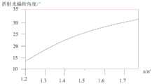
图15是对比例所提供的防窥膜的防窥模式下的角亮度图;Fig. 15 is the angular brightness diagram under the privacy protection mode of the privacy protection film provided by the comparative example;
图16是本公开实施例所提供的防窥膜的防窥模式下的角亮度图;16 is an angular brightness diagram of the privacy protection film provided by an embodiment of the present disclosure in a privacy protection mode;
图17所示的是模拟观测防窥膜的观测方向的示意图。FIG. 17 is a schematic diagram showing a simulated observation direction of the privacy film.
具体实施方式Detailed ways
以下结合附图对本公开的具体实施方式进行详细说明。应当理解的是,此处所描述的具体实施方式仅用于说明和解释本公开,并不用于限制本公开。The specific embodiments of the present disclosure will be described in detail below with reference to the accompanying drawings. It should be understood that the specific embodiments described herein are only used to illustrate and explain the present disclosure, but not to limit the present disclosure.
作为本公开的第一个方面,提供一种防窥膜,其中,如图1至图3所示,所述防窥膜包括透光的膜本体110、电泳液120、第一电极图形130和第二电极图形140。膜本体110包括入光面110a和出光面110b,第一电极图形130和第二电极图形140沿所述防窥膜的厚度方向(即,图1至图3中的竖直方向)间隔设置,膜本体110内部形成有多个容纳腔,电泳液120设置在所述容纳腔内,并且,电泳液位于第一电极图形130和第二电极图形140之间。As a first aspect of the present disclosure, a privacy protection film is provided, wherein, as shown in FIG. 1 to FIG. 3 , the privacy protection film includes a light-transmitting
电泳液120包括分散介质121和电泳粒子122,此处,分散介质121为透明介质,电泳粒子122由吸光材料(例如,黑色材料)制成。分散介质121的折射率n4小于膜本体110的折射率。并且,延伸方向一致的相邻两条所述容纳腔之间的距离为预定距离。可以根据具体的需要来确定所述预定距离。The
需要指出的是,当所述防窥膜与显示面板配合使用时,所述防窥膜与所述显示面板层叠设置。It should be pointed out that when the privacy protection film is used in conjunction with the display panel, the privacy protection film and the display panel are arranged in layers.
图1中所示的是防窥膜的一个防窥单元的示意图,并且,图1中所示的防窥膜的处于共享模式时的示意图。此时,向第一电极图形130和第二电极图形140施加电压,第一电极图形130和第二电极图形140之间形成电场,电泳液120中的电泳粒子122在电场的作用下堆积在所述容纳腔的底部,并不会妨碍从所述防窥膜的入光面入射的光线的出射。FIG. 1 is a schematic diagram of a privacy protection unit of the privacy protection film, and a schematic diagram of the privacy protection film shown in FIG. 1 is in a sharing mode. At this time, a voltage is applied to the
图4中所示的是图1中所示的防窥单元处于防窥模式时的示意图。此时,不向第一电极图形130施加第一电压、向第二电极图形140施加第二电压,第一电极图形130和第二电极图形140之间未形成电场,电泳粒子122不受电场控制,从而分散在电泳液121中,在第一电极130和第二电极图形140之间形成为阻挡壁。FIG. 4 is a schematic diagram of the privacy protection unit shown in FIG. 1 when it is in a privacy protection mode. At this time, the first voltage is not applied to the
由于分散介质121的折射率n4小于膜本体110的折射率,因此,相对于膜本体110而言,分散介质121属于光疏介质,因此,部分光(入射角大于临界角的光,在图4中用光线①表示)从作为光密介质膜本体110传导至膜本体110与作为光疏介质分散介质121之间的界面时会发生全反射、并最终从出光面110b出射,而非继续传导至分散介质121中直至被电泳粒子122吸收。由此可知,利用本公开所提供的防窥膜实现显示面板的防窥模式时,出光量较大,从而可以使得包括所述防窥膜的显示装置在防窥模式下的显示亮度。Since the refractive index n4 of the
下面结合图5和图6详细介绍本公开所提供的防窥膜能够提高显示装置亮度的原理。The principle that the privacy protection film provided by the present disclosure can improve the brightness of the display device will be described in detail below with reference to FIG. 5 and FIG. 6 .
如图5中所示,光线从光疏介质进入光密介质,光线会向竖直方向偏转(入射角为θ1,出射角为θ2,其中,θ1>θ2),光线的偏转规律如图6所示,同角度入射光,光密介质的折射率越大光线偏转角越大,即收敛程度越大,其偏转规律可以用公式(1)描述:As shown in Figure 5, when light enters the optically dense medium from an optically rarer medium, the light will be deflected in the vertical direction (the incident angle is θ1 , and the exit angle is θ2 , where θ1 >θ2 ). As shown in Figure 6, for incident light at the same angle, the greater the refractive index of the optically dense medium, the greater the deflection angle of the light, that is, the greater the degree of convergence. The deflection law can be described by formula (1):

其中,n’为光疏介质折射率;Among them, n' is the refractive index of optically rarer medium;
n为光密介质折射率;n is the refractive index of the optically dense medium;
Δθ为入射光的偏转角度,并且Δθ=θ1-θ2。Δθ is the deflection angle of the incident light, and Δθ=θ1 −θ2 .
通过公式(1)可知,n’与n的比值越大,则光线偏转角度Δθ越大。It can be known from formula (1) that the larger the ratio of n' to n, the larger the light deflection angle Δθ.
假设O点入射光为朗伯体,光通量可以用公式(2)表述,其中0°≤θ≤90°。Assuming that the incident light at point O is Lambertian, the luminous flux can be expressed by formula (2), where 0°≤θ≤90°.

其中,Φ为光通量;Among them, Φ is the luminous flux;
dS为朗伯微面元;dS is Lambertian microfacet;
L为入射光的亮度;L is the brightness of the incident light;
θ为入射光的入射角。θ is the incident angle of the incident light.
折射光夹角θ2越小,说明光线越集中,光线射出可能性越大。反之,θ2越大,光线越容易被电泳粒子吸收,降低光效。假设存在一个临界角度λ,当折射角θ2≤λ,这部分光线大概率不会被电泳粒子吸收,可以从防窥膜射出且出射角度满足防窥要求。这部分光线的光通量可以由公式(3)中的Φ1表示。由公式(3)可知,n2/n0比值越大,有效光通量越大,光效越高,其中,n0为空气折射率。The smaller the angle θ2 of the refracted light, the more concentrated the light, and the greater the possibility of the light being emitted. Conversely, the larger the θ2 , the easier the light is absorbed by the electrophoretic particles, reducing the light efficiency. Assuming that there is a critical angle λ, when the refraction angle θ2≤λ, this part of the light is unlikely to be absorbed by the electrophoretic particles, and can be emitted from the privacy protection film and the exit angle meets the privacy protection requirements. The luminous flux of this part of the light can be represented by Φ1 in formula (3). It can be known from formula (3) that the larger the ratio of n2/n0, the greater the effective luminous flux and the higher the luminous efficiency, where n0 is the refractive index of air.

光线穿过第一基板射出防窥膜的过程是从光密介质进入光疏介质,根据折射定理可知光线会发散射出,即光线方向会向水平方向倾斜。为了解决这个问题,本专利每个电泳单元出光面设计了一个收光曲面,如图4所示,曲面凸起部位于两个容纳槽中心的正上方,入光点O为所述曲面凸起部对应的部分形成的凸透镜的焦点,O点折射光透射在曲面上会转化了准直光。满足同等防窥规格的基础上,通过设置曲面凸起部可增大相邻两个容纳腔之间的距离,或者降低容纳腔的深度,从而可以有效降低容纳腔的加工难度和加工成本,提高光效,降低模组厚度。The process of the light passing through the first substrate and exiting the anti-peeping film is from the optically denser medium to the optically sparser medium. According to the theorem of refraction, the light will be scattered, that is, the direction of the light will be inclined to the horizontal direction. In order to solve this problem, a light-receiving curved surface is designed on the light-emitting surface of each electrophoresis unit in this patent. As shown in FIG. 4 , the convex portion of the curved surface is located directly above the centers of the two accommodating grooves, and the light incident point O is the convex surface of the curved surface. The focal point of the convex lens formed by the corresponding part of the part, the refracted light at the O point is transmitted on the curved surface and the collimated light will be converted. On the basis of meeting the same privacy protection specifications, the distance between two adjacent accommodating cavities can be increased by setting the convex part of the curved surface, or the depth of the accommodating cavity can be reduced, so that the processing difficulty and processing cost of the accommodating cavity can be effectively reduced and improved. Light effect, reduce module thickness.
假设容纳腔顶部到入光面距离为h1,第二基板厚度为h2,第一基板的厚度为h3,曲面焦距f=h2+h3。It is assumed that the distance from the top of the accommodating cavity to the light incident surface is h1, the thickness of the second substrate is h2, the thickness of the first substrate is h3, and the focal length of the curved surface is f=h2+h3.
假设相邻两个容纳腔的侧壁之间的间距为d1,容纳腔的宽度为d2,则防窥单元的周期l=d1+d2。Assuming that the distance between the side walls of two adjacent accommodating cavities is d1, and the width of the accommodating cavity is d2, the period l=d1+d2 of the privacy protection unit.
假设直接透射在收光曲面上的光线最大角度为α,为了满足出射光的防窥要求必然存在一个临界角度σ(即,从所述防窥膜的入光侧投射在所述曲面凸起部上的光线的最大发散角,通常可取20°<σ<60°,作为一种可选实施方式,σ可以为30°),使得α≤σ,σ与防窥膜的尺寸可由公式(4)表示:Assuming that the maximum angle of the light directly transmitted on the light-receiving curved surface is α, in order to meet the privacy requirements of the outgoing light, there must be a critical angle σ (that is, the projection from the light incident side of the privacy film on the convex portion of the curved surface The maximum divergence angle of the light on , usually 20°<σ<60°, as an optional implementation, σ can be 30°), so that α≤σ, σ and the size of the privacy film can be determined by formula (4) express:

假设分散介质折射率为n4,第一基板折射率为n1,在本公开中,n4<n1,如此光线可实现两种功能,如图7所示,当光线入射角θ3’小于全反射角(大视角光)时,光线会进入电泳液,被电泳粒子吸收,当入射角θ3大于全反射角时,光线会在电泳槽表面发生全反射,射出电泳膜。由此可知,合理设计基板和电泳液的折射搭配,便可利用全反射特性,筛选特定视角光线,防止窄视角光线被电泳吸收,造成光效降低。Assuming that the refractive index of the dispersion medium is n4 and the refractive index of the first substrate is n1, in the present disclosure, n4<n1, so the light can achieve two functions, as shown in FIG. 7, when the light incident angle θ3' is smaller than the total reflection angle ( When the incident angle θ3 is greater than the total reflection angle, the light will be totally reflected on the surface of the electrophoresis tank, and the electrophoretic film will be emitted. It can be seen from this that, by rationally designing the refraction matching of the substrate and the electrophoresis liquid, the total reflection characteristic can be used to screen the light with a specific viewing angle, so as to prevent the narrow viewing angle light from being absorbed by electrophoresis, resulting in a decrease in light efficiency.
光线规律可以用公式(5)描述:The light law can be described by formula (5):

根据防窥要求,假设全反射光与竖直方向的夹角需要满足一个临界值,才能保证光线射出后不会形成大视角杂光,该临界值为δ(即,δ为从所述容纳腔的侧壁上反射的光线的最大发散角,通常可取20°<σ<60°,作为一种可选实施方式,δ可以为30°),则θ6≤δ,分散介质的折射率n4和第一基板的n1的设计值必须满足公式(6)。According to the privacy protection requirements, it is assumed that the angle between the total reflected light and the vertical direction needs to meet a critical value to ensure that no large viewing angle stray light will be formed after the light is emitted. The maximum divergence angle of the light reflected on the sidewall of , usually 20°<σ<60°, as an optional implementation, δ can be 30°), then θ6≤δ, the refractive index of the dispersion medium n4 and the first The design value of n1 for a substrate must satisfy formula (6).

由于透光部的表面为曲面凸起部1102a,因此,该透光部能够对在该透光部内传播的发散光进行聚拢,既能够提高出光亮度,又可以保证防窥效果。Since the surface of the light-transmitting portion is a curved
可选地,所述透光部形成为一个凸透镜。所述凸透镜可以将焦点处发出的发散光转换为准直光。与发散光相比,准直光具有较高的亮度。Optionally, the light-transmitting portion is formed as a convex lens. The convex lens can convert the divergent light emitted at the focal point into collimated light. Compared with divergent light, collimated light has higher brightness.
在本公开中,对曲面凸起部1102a的具体几何特征不做特殊的限定。为了将尽量多的入射光转换为准直光,可选地,曲面凸起部1102a对应的凸透镜的焦点O位于入光面110b上,或者,如图4所示,曲面凸起部1102a对应的凸透镜的焦点O位于入光面110b的外侧。In the present disclosure, the specific geometric features of the curved
至本公开中,对第一电极图形130、以及第二电极图形140的具体结构均不做特殊的限定。In the present disclosure, the specific structures of the
作为一种可选实施方式,如图1和图3所示,第一电极图形130包括多个第一电极130a,每个所述容纳腔内均设置有至少一个第一电极130a。As an optional implementation manner, as shown in FIGS. 1 and 3 , the
由于不同的容纳腔内的第一电极130互相独立,因此,可以独立地控制防窥膜不同位置的出光状态,从而能够更好地满足各种不同的应用场景。Since the
在本公开中,对如何将第一电极130a设置在所述容纳腔内、以及设置在容纳腔内的何种位置不做特殊的限定。作为一种可选实施方式,可以将第一电极130a设置在容纳腔的顶面上,其中,所述容纳腔的顶面为所述容纳腔上朝向所述出光面的表面。如图4所示,停止向第二电极图形140和第一电极130a施加电压后,电泳粒子形成的阻挡壁与容纳腔的侧壁之间存在间隙,该间隔中充满了分散介质121,从而可以确保满足临界角的入射光在膜本体110和分散介质121之间的界面处发生全反射、而非被电泳粒子122吸收。In the present disclosure, how to dispose the
在第一电极图形130包括多个第一电极130a的情况中,又可以通过两种不同的方式设置所述容纳腔。In the case where the
具体地,膜本体110包括第一基板111和第二基板112,第一基板111和第二基板112贴合,第二基板112背离第一基板111的表面为入光面110b,第一基板111背离第二基板112的表面为出光面110a。Specifically, the
在图1和图8中所示的实施方式中,所述容纳腔形成在所述第一基板111内。具体地,在制造所述防窥膜时,先在第一基板111上形成具有开口的容纳腔,在该容纳腔内形成第一电极130,并在所述容纳腔内以喷墨打印(或者其他方式)设置电泳液,然后将第一基板111与第二基板112设置在一起形成膜本体时,可以将容纳腔的开口封闭。In the embodiments shown in FIGS. 1 and 8 , the receiving cavity is formed in the
在图3和图10中所示的实施方式中,所述容纳腔包括形成在所述第一基板111上的第一容纳槽和形成在第二基板112上的第二容纳槽。在制造所述防窥膜时,可以分别在第一基板111制造第一容纳槽、以及在的第二基板112上制造第二容纳槽,在第一容纳槽中设置电泳液、以及在第二容纳槽内设置电泳液,将第一基板111和第二基板112贴合时,第一容纳槽和第二容纳槽可以拼成一个容纳腔。In the embodiments shown in FIGS. 3 and 10 , the accommodating cavity includes a first accommodating groove formed on the
当然,本发明并不限于此,在图2和图9中所示的实施方式中,第一电极图形130为整面电极,并且,第一电极图形130设置在第一基板111和第二基板112之间,所述容纳腔形成在第二基板112内。在制造所述防窥膜时,先在第二基板112上形成具有开口的容纳腔,在该容纳腔内形成第一电极130,并在所述容纳腔内以喷墨打印(或者其他方式)设置电泳液,然后将第一基板111与第二基板112设置在一起形成膜本体时,可以将容纳腔的开口封闭。Of course, the present invention is not limited thereto. In the embodiments shown in FIG. 2 and FIG. 9 , the
在本发明中,对第一基板111的折射率n1和第二基板112的折射率n2不做特殊的限定。但是,需要指出的是,分散介质121的折射率n4小于第一基板111的折射率n1,并且,分散介质121的折射率n4小于第二基板112的折射率n2。In the present invention, the refractive index n1 of the
在本公开中,对如何将第一基板111以及第二基板112连接并不做特殊的限制,可选地,第一基板111和第二基板112通过透明粘结剂层113互相连接,透明粘结剂层113的折射率n3与第一基板111的折射率n1或者第二基板112的折射率n2相同。In the present disclosure, how to connect the
当然,本发明并非局限于此,例如,可以预先设置具有容纳腔、以及第一电极的透明盒,将电泳液120封闭在该透明盒内,然后再设置形成膜本体110的材料,并最终获得所述防窥膜。Of course, the present invention is not limited to this. For example, a transparent box with an accommodating cavity and a first electrode can be set in advance, the
在本公开中,对第二电极图形140的具体结构也不做特殊的限定。例如,第二电极图形也可以包括多个独立设置的第二电极。为了便于设置,第二电极图形140为整面电极。为了确保光线能够正常入射,第二电极图形140由透明电极材料制成,且第二电极图形140位于入光面110b的入光侧。In the present disclosure, the specific structure of the
为了进一步提高从防窥膜出射的光的量,可选地,所述防窥膜还包括至少一个反射层150,至少一个所述容纳腔的底面设置有反射层150。具体地,所述容纳腔的底面为所述容纳腔上朝向入光面110a的表面。In order to further increase the amount of light emitted from the privacy protection film, optionally, the privacy protection film further includes at least one
光线照射在反射层150上时,会被该反射层150反射,而不会进一步进入容纳腔而被电泳粒子122吸收。When the light is irradiated on the
需要指出的是,设置反射层150不仅可以提高显示装置在防窥模式下的亮度,还可以提高反射层150在共享模式下的亮度。It should be pointed out that the provision of the
如图4所示,当入射光③照射在容纳腔底部对应的位置时,直接被反射层150反射至第二电极图形140的表面,而非被电泳粒子122所吸收,被反射回第二电极图形140的光线由第二电极图形140反射至膜本体的透光部,并最终从所述透光部出射。As shown in FIG. 4 , when the
在本公开中,对反射层150的具体材料不做特殊的限定。例如,反射层150的材料可以为高反白油(反射率>85%),反射层150还可以为镀银层(反射率>90%)、镀铝层(反射率>90%)。再例如,反射层150还可以为镀非金属高低折射率镀层,例如,SiO2/TiO2,其反射率可超过95%。In the present disclosure, the specific material of the
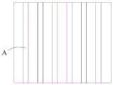
在本公开中,对容纳腔的排列并不做特殊的限制,如仅要求在一个方向上防窥,那么,多条所述容纳腔A互相平行,如图11所示。In the present disclosure, the arrangement of the accommodating cavities is not particularly limited, if only requiring privacy protection in one direction, then a plurality of the accommodating cavities A are parallel to each other, as shown in FIG. 11 .
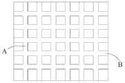
如果要求在两个方向上防窥,如图12所示,多条所述容纳腔互相交错(横向容纳腔B和纵向容纳腔A交错),将所述防窥膜划分为多个透光部。If privacy protection is required in two directions, as shown in FIG. 12 , a plurality of the accommodating cavities are staggered with each other (the transverse accommodating cavity B and the longitudinal accommodating cavity A are staggered), and the privacy protection film is divided into a plurality of light-transmitting parts .
作为本公开的第二个方面,提供一种背光源,如图13所示,所述背光源包括发光面板200,其中,所述背光源还包括本发明所提供的上述防窥膜,所述防窥膜的入光面110b与发光面板200的出光面相对设置。As a second aspect of the present disclosure, a backlight source is provided. As shown in FIG. 13 , the backlight source includes a light-emitting
本公开所提供的背光源与不能够主动发光的显示面板(例如,液晶显示面板、电致变色显示面板等)配合使用,从而可以实现显示面板在防窥模式、以及共享模式两种模式下进行显示,满足不同的用户需求。The backlight provided by the present disclosure is used in conjunction with a display panel that cannot actively emit light (eg, liquid crystal display panel, electrochromic display panel, etc.) Display to meet different user needs.
在本公开中,对发光面板200的具体结构不做特殊的限定。作为一种可选实施方式,发光面板200包括依次层叠设置的LED灯板210和扩散板220。LED灯板包括排列为阵列的多个LED,扩散板220可以将点光源转换为面光源,从而使得发光面板220的出光更加均匀。In the present disclosure, the specific structure of the
作为一种可选实施方式,发光面板200还可以包括量子点膜230,为了使得发光面板200发出白光,可选地,LED灯板发蓝光,量子点膜230可以在蓝光的激发下发出白光。As an optional embodiment, the light-emitting
为了提高发光面板200的出光亮度,可选地,发光面板200还可以包括棱镜膜240。具体地,LED灯板210、扩散板220、量子点膜230、棱镜膜240依次层叠设置。In order to improve the light-emitting brightness of the light-emitting
如上文中所述,所述背光源可以与液晶显示面板配合使用。为了避免背光源的出射光被液晶显示面板的下偏光片所吸收,可选地,所述背光源还可以包括设置在所述防窥膜的出光侧的反射偏光片300。可选地,反射偏光片300可以为一种DBEF膜片。As mentioned above, the backlight source can be used in conjunction with a liquid crystal display panel. In order to prevent the outgoing light of the backlight source from being absorbed by the lower polarizer of the liquid crystal display panel, optionally, the backlight source may further include a
作为本公开的第三个方面,提供一种显示装置,所述显示装置包括显示面板和本公开所提供的上述背光源。As a third aspect of the present disclosure, a display device is provided, the display device includes a display panel and the above-mentioned backlight provided by the present disclosure.
通过对第一电极图形和第二电极图形施加电压,可以使得显示装置在共享模式和防窥模式之间切换。并且,由于使用了本公开所提供的防窥膜,所述显示装置在防窥模式下具有较高的显示亮度,从而使得所述显示装置具有较低的能耗。By applying a voltage to the first electrode pattern and the second electrode pattern, the display device can be switched between the sharing mode and the privacy mode. Moreover, due to the use of the privacy protection film provided by the present disclosure, the display device has higher display brightness in the privacy protection mode, so that the display device has lower power consumption.
在本公开中,对显示面板的具体类型不做特殊的限定。例如,所述显示面板可以是液晶显示面板、电致变色显示面板等非主动发光显示面板。In the present disclosure, the specific type of the display panel is not particularly limited. For example, the display panel may be a non-active light-emitting display panel such as a liquid crystal display panel, an electrochromic display panel, or the like.
当所述显示面板为液晶显示面板时,所述显示装置还包括发光面板,所述防窥膜设置在所述发光面板之间,所述防窥膜的出光面朝向所述显示面板,所述防窥膜的入光面朝向所述背光源。换言之,当所述显示面板为液晶显示面板时,所述显示装置还包括本公开第二个方面所提供的背光源。When the display panel is a liquid crystal display panel, the display device further includes a light-emitting panel, the privacy protection film is disposed between the light-emitting panels, and the light-emitting surface of the privacy protection film faces the display panel, and the privacy protection film faces the display panel. The light incident surface of the privacy film faces the backlight. In other words, when the display panel is a liquid crystal display panel, the display device further includes the backlight provided by the second aspect of the present disclosure.
实施例Example
图1和图8中所示的防窥膜,其中,该防窥膜的参数如表1中所示。The privacy film shown in FIG. 1 and FIG. 8 , wherein the parameters of the privacy film are shown in Table 1.
对比例Comparative ratio
如图14所述,所述防窥膜包括第一基板111(折射率n1)、第二基板112(折射率n2),第一基板111和第二基板112通过粘结剂层113(折射率n3)粘结,第一基板111内形成有容纳腔,容纳腔内设置有电泳液120(包括分散介质121和电泳粒子122,分散介质折射率为n4)。对比例的防窥膜参数如表1所示。As shown in FIG. 14 , the privacy film includes a first substrate 111 (refractive index n1), a second substrate 112 (refractive index n2), and the
表1Table 1

通过Lighttools进行从防窥膜左右两侧观看的模拟、以及从防窥膜上下两侧光看的模拟,分别获得对比例和实施例中两种防窥膜的防窥模式下的角亮度图。其中,此处的“上下”、“左右”是以图17为基准的方向。The simulation of viewing from the left and right sides of the privacy protection film and the simulation of viewing from the upper and lower sides of the privacy protection film are performed through Lighttools, and the angular luminance maps of the privacy protection modes of the two privacy protection films in the comparative example and the embodiment are obtained respectively. Here, "up and down" and "right and left" are directions based on FIG. 17 .
如图15所示,对比例的模拟结果中,中心角亮度为4600nit,半亮度角为±15°,截止角为±30°。其中,在图15中实线曲线表示的是,模拟防窥膜的上下两侧观看获得的亮度曲线,虚线曲线表示的是,模拟从防窥膜的左右两侧观看获得的亮度曲线。As shown in Figure 15, in the simulation results of the comparative example, the center angle brightness is 4600 nit, the half brightness angle is ±15°, and the cutoff angle is ±30°. 15 , the solid line curve represents the brightness curve obtained by simulating the upper and lower sides of the privacy protection film, and the dotted line curve represents the brightness curve obtained by simulating the privacy protection film viewed from the left and right sides.
如图16所示,实施例的模拟结果中,中心角亮度为7500nit,半亮度角为±12°,截止角为±26°。其中,在图16中实线曲线表示的是,模拟防窥膜的上下两侧观看获得的亮度曲线,虚线曲线表示的是,模拟从防窥膜的左右两侧观看获得的亮度曲线。As shown in FIG. 16 , in the simulation results of the embodiment, the center angle luminance is 7500 nit, the half luminance angle is ±12°, and the cutoff angle is ±26°. 16 , the solid line curve represents the brightness curve obtained by simulating the upper and lower sides of the privacy protection film, and the dotted line curve represents the brightness curve obtained by simulating the privacy protection film viewed from the left and right sides.
由此可知,容纳腔之间的间距相同、防窥膜厚度相同、材料相同的情况下,增加反射层、以及设置曲面凸起部,实施例所提供的防窥膜的亮度比对比例中的防窥膜的亮度提升了63%,左右两侧的半亮度角缩小了3°,左右两侧的截止角缩小了4°。It can be seen from this that, when the distance between the accommodating cavities is the same, the thickness of the privacy film is the same, and the material is the same, the reflective layer is added, and the convex portion of the curved surface is provided. The brightness of the privacy film is increased by 63%, the half-brightness angle on the left and right sides is reduced by 3°, and the cut-off angle on the left and right sides is reduced by 4°.
模拟对比例中所提供的防窥膜的防窥模式照度图,得知其照度平均值为4340lux,照度均一性为85%。By simulating the privacy mode illuminance map of the privacy film provided in the comparative example, it is known that the average illuminance is 4340 lux, and the illuminance uniformity is 85%.
模拟实施中所提供的防窥膜的防窥模式照度图,得知其照度平均值为5750lux,照度均一性为88.9%。By simulating the privacy-proof mode illuminance diagram of the privacy-proof film provided in the implementation, it is known that the average illuminance is 5750 lux, and the illuminance uniformity is 88.9%.
由此可知,实施例所提供的防窥膜亮度提高32%,照度均一性提高了3.9%。It can be seen that the brightness of the privacy protection film provided by the embodiment is increased by 32%, and the uniformity of illumination is increased by 3.9%.
可以理解的是,以上实施方式仅仅是为了说明本公开的原理而采用的示例性实施方式,然而本公开并不局限于此。对于本领域内的普通技术人员而言,在不脱离本公开的精神和实质的情况下,可以做出各种变型和改进,这些变型和改进也视为本公开的保护范围。It should be understood that the above embodiments are merely exemplary embodiments adopted to illustrate the principles of the present disclosure, but the present disclosure is not limited thereto. For those skilled in the art, various modifications and improvements can be made without departing from the spirit and essence of the present disclosure, and these modifications and improvements are also regarded as the protection scope of the present disclosure.
Claims (15)
Translated fromChinese

Priority Applications (2)
| Application Number | Priority Date | Filing Date | Title |
|---|---|---|---|
| CN202010156961.7ACN111323982B (en) | 2020-03-09 | 2020-03-09 | Peep-proof film, backlight source and display device |
| US17/195,779US11835804B2 (en) | 2020-03-09 | 2021-03-09 | Peep-proof film, backlight source and display device |
Applications Claiming Priority (1)
| Application Number | Priority Date | Filing Date | Title |
|---|---|---|---|
| CN202010156961.7ACN111323982B (en) | 2020-03-09 | 2020-03-09 | Peep-proof film, backlight source and display device |
Publications (2)
| Publication Number | Publication Date |
|---|---|
| CN111323982Atrue CN111323982A (en) | 2020-06-23 |
| CN111323982B CN111323982B (en) | 2023-07-21 |
Family
ID=71171426
Family Applications (1)
| Application Number | Title | Priority Date | Filing Date |
|---|---|---|---|
| CN202010156961.7AActiveCN111323982B (en) | 2020-03-09 | 2020-03-09 | Peep-proof film, backlight source and display device |
Country Status (2)
| Country | Link |
|---|---|
| US (1) | US11835804B2 (en) |
| CN (1) | CN111323982B (en) |
Cited By (13)
| Publication number | Priority date | Publication date | Assignee | Title |
|---|---|---|---|---|
| CN112904637A (en)* | 2021-02-01 | 2021-06-04 | 义乌清越光电科技有限公司 | Electrochromic display and preparation method thereof |
| CN113094766A (en)* | 2021-03-31 | 2021-07-09 | 维沃移动通信有限公司 | Display panel, display method, display device, display equipment, preparation method and storage medium |
| CN114895392A (en)* | 2022-05-17 | 2022-08-12 | 深圳市雕拓科技有限公司 | Peep-proof film and display device |
| CN116224668A (en)* | 2021-12-01 | 2023-06-06 | 北京小米移动软件有限公司 | Peep-proof screen, peep-proof method, peep-proof device, electronic equipment and medium |
| CN116482887A (en)* | 2023-03-30 | 2023-07-25 | 惠科股份有限公司 | Display device, control circuit and vehicle |
| CN116500821A (en)* | 2023-03-30 | 2023-07-28 | 惠科股份有限公司 | Display panel, control circuit and display device |
| CN116540466A (en)* | 2023-03-30 | 2023-08-04 | 惠科股份有限公司 | Peep-proof structure, control circuit and display device |
| CN116794898A (en)* | 2023-05-31 | 2023-09-22 | 绵阳惠科光电科技有限公司 | Display panel and display device |
| CN116991011A (en)* | 2023-09-27 | 2023-11-03 | 惠科股份有限公司 | Display panel, driving method and display device |
| WO2023231095A1 (en)* | 2022-05-31 | 2023-12-07 | Tcl华星光电技术有限公司 | Peep-proof protection film and preparation method therefor, and splicing panel |
| CN117950218A (en)* | 2024-02-19 | 2024-04-30 | 武汉华星光电技术有限公司 | Privacy film and display terminal |
| WO2024198402A1 (en)* | 2023-03-28 | 2024-10-03 | 武汉华星光电技术有限公司 | Display module and display apparatus |
| US12153234B2 (en) | 2022-05-31 | 2024-11-26 | Tcl China Star Optoelectronics Technology Co., Ltd. | Privacy film and splice panel |
Families Citing this family (7)
| Publication number | Priority date | Publication date | Assignee | Title |
|---|---|---|---|---|
| WO2023049481A1 (en)* | 2021-09-27 | 2023-03-30 | E Ink Corporation | Electrophoretic particle film having reduced diffraction in an open state |
| CN114460785A (en)* | 2022-01-24 | 2022-05-10 | 广东以诺通讯有限公司 | Intelligent terminal with electrochromic peep-proof layer and control method and device thereof |
| CN114937419B (en)* | 2022-07-22 | 2022-10-21 | 联宝(合肥)电子科技有限公司 | Peep-proof film, electronic equipment and display method |
| CN116088224B (en)* | 2023-02-27 | 2023-06-30 | 惠科股份有限公司 | Backlight module, display device and display driving method |
| CN118859562A (en)* | 2023-04-27 | 2024-10-29 | 瀚宇彩晶股份有限公司 | Anti-peeping element and method for manufacturing the same |
| CN117970546B (en)* | 2024-04-01 | 2024-06-11 | 苏州弘德光电材料科技有限公司 | Light control film and display device |
| CN118401040B (en)* | 2024-04-29 | 2025-05-23 | 惠科股份有限公司 | Display panel and display device thereof |
Citations (13)
| Publication number | Priority date | Publication date | Assignee | Title |
|---|---|---|---|---|
| JP2004054029A (en)* | 2002-07-22 | 2004-02-19 | Sharp Corp | Display device and method of manufacturing the same |
| CN1804733A (en)* | 2005-01-12 | 2006-07-19 | 精工爱普生株式会社 | Electro-optical device, image printing apparatus, and method of manufacturing electro-optical device |
| EP1818713A1 (en)* | 2006-02-14 | 2007-08-15 | Seiko Epson Corporation | Electro-optic device, method for manufacturing electro-optic device, projector, and electronic apparatus |
| JP2007240903A (en)* | 2006-03-09 | 2007-09-20 | Sony Corp | Optical control element and display device |
| JP2008185767A (en)* | 2007-01-30 | 2008-08-14 | Toppan Printing Co Ltd | Optical film and manufacturing method thereof |
| US20100141573A1 (en)* | 2008-12-05 | 2010-06-10 | Craig Lin | Luminance enhancement structure with moire reducing design |
| CN103827726A (en)* | 2011-09-30 | 2014-05-28 | 3M创新有限公司 | Electronically switchable privacy film and display device with electronically switchable privacy film |
| US20160077363A1 (en)* | 2014-09-12 | 2016-03-17 | Nlt Technologies, Ltd. | Optical element, and display device, electronic apparatus, lighting device using the same |
| CN105629354A (en)* | 2016-01-04 | 2016-06-01 | 京东方科技集团股份有限公司 | Peep-proof membrane, manufacture method and display device |
| TWI563325B (en)* | 2015-12-04 | 2016-12-21 | Young Lighting Technology Inc | Light source module and display apparatus |
| CN109270698A (en)* | 2018-11-22 | 2019-01-25 | 合肥京东方光电科技有限公司 | Light collimating film and its application |
| CN109683421A (en)* | 2019-03-06 | 2019-04-26 | 京东方科技集团股份有限公司 | A kind of adjustable refractive index method, apparatus, intelligent window and the vehicles |
| CN109991791A (en)* | 2017-12-11 | 2019-07-09 | 天马日本株式会社 | The driving method of beam direction control device and beam direction control element |
Family Cites Families (2)
| Publication number | Priority date | Publication date | Assignee | Title |
|---|---|---|---|---|
| CA3087197C (en)* | 2018-10-15 | 2021-09-07 | Ozzie's Enterprises LLC | Borehole mapping tool and methods of mapping boreholes |
| JP2020091434A (en)* | 2018-12-06 | 2020-06-11 | 株式会社ジャパンディスプレイ | Electro-optical element and storage container including electro-optical element |
- 2020
- 2020-03-09CNCN202010156961.7Apatent/CN111323982B/enactiveActive
- 2021
- 2021-03-09USUS17/195,779patent/US11835804B2/enactiveActive
Patent Citations (13)
| Publication number | Priority date | Publication date | Assignee | Title |
|---|---|---|---|---|
| JP2004054029A (en)* | 2002-07-22 | 2004-02-19 | Sharp Corp | Display device and method of manufacturing the same |
| CN1804733A (en)* | 2005-01-12 | 2006-07-19 | 精工爱普生株式会社 | Electro-optical device, image printing apparatus, and method of manufacturing electro-optical device |
| EP1818713A1 (en)* | 2006-02-14 | 2007-08-15 | Seiko Epson Corporation | Electro-optic device, method for manufacturing electro-optic device, projector, and electronic apparatus |
| JP2007240903A (en)* | 2006-03-09 | 2007-09-20 | Sony Corp | Optical control element and display device |
| JP2008185767A (en)* | 2007-01-30 | 2008-08-14 | Toppan Printing Co Ltd | Optical film and manufacturing method thereof |
| US20100141573A1 (en)* | 2008-12-05 | 2010-06-10 | Craig Lin | Luminance enhancement structure with moire reducing design |
| CN103827726A (en)* | 2011-09-30 | 2014-05-28 | 3M创新有限公司 | Electronically switchable privacy film and display device with electronically switchable privacy film |
| US20160077363A1 (en)* | 2014-09-12 | 2016-03-17 | Nlt Technologies, Ltd. | Optical element, and display device, electronic apparatus, lighting device using the same |
| TWI563325B (en)* | 2015-12-04 | 2016-12-21 | Young Lighting Technology Inc | Light source module and display apparatus |
| CN105629354A (en)* | 2016-01-04 | 2016-06-01 | 京东方科技集团股份有限公司 | Peep-proof membrane, manufacture method and display device |
| CN109991791A (en)* | 2017-12-11 | 2019-07-09 | 天马日本株式会社 | The driving method of beam direction control device and beam direction control element |
| CN109270698A (en)* | 2018-11-22 | 2019-01-25 | 合肥京东方光电科技有限公司 | Light collimating film and its application |
| CN109683421A (en)* | 2019-03-06 | 2019-04-26 | 京东方科技集团股份有限公司 | A kind of adjustable refractive index method, apparatus, intelligent window and the vehicles |
Cited By (17)
| Publication number | Priority date | Publication date | Assignee | Title |
|---|---|---|---|---|
| CN112904637A (en)* | 2021-02-01 | 2021-06-04 | 义乌清越光电科技有限公司 | Electrochromic display and preparation method thereof |
| CN113094766A (en)* | 2021-03-31 | 2021-07-09 | 维沃移动通信有限公司 | Display panel, display method, display device, display equipment, preparation method and storage medium |
| CN113094766B (en)* | 2021-03-31 | 2025-06-20 | 维沃移动通信有限公司 | Display panel, display method, device, equipment, preparation method and storage medium |
| CN116224668A (en)* | 2021-12-01 | 2023-06-06 | 北京小米移动软件有限公司 | Peep-proof screen, peep-proof method, peep-proof device, electronic equipment and medium |
| CN114895392A (en)* | 2022-05-17 | 2022-08-12 | 深圳市雕拓科技有限公司 | Peep-proof film and display device |
| WO2023231095A1 (en)* | 2022-05-31 | 2023-12-07 | Tcl华星光电技术有限公司 | Peep-proof protection film and preparation method therefor, and splicing panel |
| US12265241B2 (en) | 2022-05-31 | 2025-04-01 | Tcl China Star Optoelectronics Technology Co., Ltd. | Privacy film, preparation method thereof and splice panel |
| US12153234B2 (en) | 2022-05-31 | 2024-11-26 | Tcl China Star Optoelectronics Technology Co., Ltd. | Privacy film and splice panel |
| WO2024198402A1 (en)* | 2023-03-28 | 2024-10-03 | 武汉华星光电技术有限公司 | Display module and display apparatus |
| CN116500821B (en)* | 2023-03-30 | 2024-06-28 | 惠科股份有限公司 | Display panel, control circuit and display device |
| CN116540466A (en)* | 2023-03-30 | 2023-08-04 | 惠科股份有限公司 | Peep-proof structure, control circuit and display device |
| CN116500821A (en)* | 2023-03-30 | 2023-07-28 | 惠科股份有限公司 | Display panel, control circuit and display device |
| CN116482887A (en)* | 2023-03-30 | 2023-07-25 | 惠科股份有限公司 | Display device, control circuit and vehicle |
| CN116794898A (en)* | 2023-05-31 | 2023-09-22 | 绵阳惠科光电科技有限公司 | Display panel and display device |
| CN116991011B (en)* | 2023-09-27 | 2024-01-12 | 惠科股份有限公司 | Display panel, driving method and display device |
| CN116991011A (en)* | 2023-09-27 | 2023-11-03 | 惠科股份有限公司 | Display panel, driving method and display device |
| CN117950218A (en)* | 2024-02-19 | 2024-04-30 | 武汉华星光电技术有限公司 | Privacy film and display terminal |
Also Published As
| Publication number | Publication date |
|---|---|
| CN111323982B (en) | 2023-07-21 |
| US20210278712A1 (en) | 2021-09-09 |
| US11835804B2 (en) | 2023-12-05 |
Similar Documents
| Publication | Publication Date | Title |
|---|---|---|
| CN111323982B (en) | Peep-proof film, backlight source and display device | |
| US11249344B2 (en) | Planar lighting device | |
| KR102312522B1 (en) | Display device | |
| KR101699058B1 (en) | Backlight assembly and display apparatus having the same | |
| JP7265459B2 (en) | Lighting device and display device | |
| CN206975244U (en) | Light guide plate, backlight module and display device | |
| CN206848653U (en) | A kind of backlight module and display device | |
| US9690034B2 (en) | Illumination device and display device | |
| TW201734602A (en) | Backlight module and display apparatus | |
| CN107315280B (en) | Backlight module and its manufacturing method, display device | |
| CN211741790U (en) | Light source module and display device | |
| CN106405918A (en) | Display panel and display device having the same | |
| CN102540495B (en) | Collimating optical element, assembly, array and collimating optical module | |
| WO2013180024A1 (en) | Illumination device, and display device | |
| TW201915982A (en) | Spliced display apparatus | |
| CN108121114A (en) | Display device with dichroic filter | |
| CN103900031B (en) | A light guide device for liquid crystal display | |
| CN108885302B (en) | Lighting and Display Devices | |
| WO2013008577A1 (en) | Illumination device and display device | |
| TW201504699A (en) | Light guide plate and backlight module incorporating the same | |
| KR20120039405A (en) | Backlight unit and liquid crystal display device having the same | |
| JP2025140457A (en) | lighting equipment | |
| JP2023069678A (en) | Lighting device and display device | |
| WO2012147650A1 (en) | Led module, backlight unit, and liquid crystal display device | |
| JP2011164472A (en) | Liquid crystal display device |
Legal Events
| Date | Code | Title | Description |
|---|---|---|---|
| PB01 | Publication | ||
| PB01 | Publication | ||
| SE01 | Entry into force of request for substantive examination | ||
| SE01 | Entry into force of request for substantive examination | ||
| GR01 | Patent grant | ||
| GR01 | Patent grant |