CN111312068A - Mini lamp bead, manufacturing method, backlight source and display device - Google Patents
Mini lamp bead, manufacturing method, backlight source and display deviceDownload PDFInfo
- Publication number
- CN111312068A CN111312068ACN202010256069.6ACN202010256069ACN111312068ACN 111312068 ACN111312068 ACN 111312068ACN 202010256069 ACN202010256069 ACN 202010256069ACN 111312068 ACN111312068 ACN 111312068A
- Authority
- CN
- China
- Prior art keywords
- light
- emitting surface
- led chip
- source
- mini
- Prior art date
- Legal status (The legal status is an assumption and is not a legal conclusion. Google has not performed a legal analysis and makes no representation as to the accuracy of the status listed.)
- Pending
Links
Images


Classifications
- G—PHYSICS
- G09—EDUCATION; CRYPTOGRAPHY; DISPLAY; ADVERTISING; SEALS
- G09F—DISPLAYING; ADVERTISING; SIGNS; LABELS OR NAME-PLATES; SEALS
- G09F9/00—Indicating arrangements for variable information in which the information is built-up on a support by selection or combination of individual elements
- H—ELECTRICITY
- H10—SEMICONDUCTOR DEVICES; ELECTRIC SOLID-STATE DEVICES NOT OTHERWISE PROVIDED FOR
- H10H—INORGANIC LIGHT-EMITTING SEMICONDUCTOR DEVICES HAVING POTENTIAL BARRIERS
- H10H20/00—Individual inorganic light-emitting semiconductor devices having potential barriers, e.g. light-emitting diodes [LED]
- H10H20/01—Manufacture or treatment
- H—ELECTRICITY
- H10—SEMICONDUCTOR DEVICES; ELECTRIC SOLID-STATE DEVICES NOT OTHERWISE PROVIDED FOR
- H10H—INORGANIC LIGHT-EMITTING SEMICONDUCTOR DEVICES HAVING POTENTIAL BARRIERS
- H10H20/00—Individual inorganic light-emitting semiconductor devices having potential barriers, e.g. light-emitting diodes [LED]
- H10H20/80—Constructional details
- H10H20/85—Packages
- H10H20/852—Encapsulations
- H—ELECTRICITY
- H10—SEMICONDUCTOR DEVICES; ELECTRIC SOLID-STATE DEVICES NOT OTHERWISE PROVIDED FOR
- H10H—INORGANIC LIGHT-EMITTING SEMICONDUCTOR DEVICES HAVING POTENTIAL BARRIERS
- H10H20/00—Individual inorganic light-emitting semiconductor devices having potential barriers, e.g. light-emitting diodes [LED]
- H10H20/80—Constructional details
- H10H20/85—Packages
- H10H20/855—Optical field-shaping means, e.g. lenses
Landscapes
- Physics & Mathematics (AREA)
- General Physics & Mathematics (AREA)
- Engineering & Computer Science (AREA)
- Theoretical Computer Science (AREA)
- Planar Illumination Modules (AREA)
Abstract
Description
Translated fromChinese技术领域technical field
本发明涉及显示技术领域,尤其涉及一种迷你灯珠、制作方法、背光源及显示设备。The invention relates to the field of display technology, in particular to a mini lamp bead, a manufacturing method, a backlight source and a display device.
背景技术Background technique
随着手机、iPad、智能电视等显示设备正向轻、薄、画质更优的方向发展。其中,迷你灯珠作为新一代显示技术,以其体积小、厚度薄、亮度高、毫米级像素分区、高精密动态背光效果等优点受到市场欢迎,如,MINI LED、迷你OLED等各种迷你发光灯珠。With the development of display devices such as mobile phones, iPads, and smart TVs, they are developing in the direction of lightness, thinness, and better picture quality. Among them, mini lamp beads, as a new generation of display technology, are popular in the market due to their advantages of small size, thin thickness, high brightness, millimeter-level pixel division, and high-precision dynamic backlight effects, such as MINI LED, mini OLED and other mini light-emitting devices. lamp beads.
然而现有的MINI LED发光角度小,基本都是正面发光,在灯珠的侧边基本没有光线射出,从而使灯珠之间的能量较少;进而,在灯珠之间产生暗区。为实现良好的成像效果,故需要将背光源上的MINI LED灯珠进行密集排布,灯珠间距在3mm左右,由此使背光源的成本增加,且在使用中功率增大、产热更多。However, the existing MINI LED has a small light-emitting angle and basically emits light from the front, and basically no light is emitted from the side of the lamp bead, so that the energy between the lamp bead is less; furthermore, a dark area is generated between the lamp bead. In order to achieve a good imaging effect, it is necessary to densely arrange the MINI LED lamp beads on the backlight source, and the distance between the lamp beads is about 3mm, which increases the cost of the backlight source, and increases the power and heat generation during use. many.
发明内容SUMMARY OF THE INVENTION
本发明的目的在于克服现有技术的缺陷,提供一种迷你灯珠、制作方法、背光源及显示设备,以扩大迷你灯珠的发光角度。The purpose of the present invention is to overcome the defects of the prior art, and to provide a mini lamp bead, a manufacturing method, a backlight source and a display device, so as to enlarge the luminous angle of the mini lamp bead.
为解决上述问题,本发明提供了:In order to solve the above-mentioned problems, the present invention provides:
一种迷你灯珠,包括:A mini lamp bead, including:
发光源;light source;
微透镜,所述微透镜罩设于所述发光源上;a micro-lens, the micro-lens cover is arranged on the light-emitting source;
所述微透镜具有第一出光面和第二出光面;所述第一出光面对应所述发光源的上方设置,所述发光源的部分光线从所述第一出光面射出;所述第二出光面对应所述发光源的侧面设置,所述发光源的部分光线从所述第二出光面射出。The microlens has a first light-emitting surface and a second light-emitting surface; the first light-emitting surface is disposed above the light-emitting source, and part of the light of the light-emitting source is emitted from the first light-emitting surface; the first light-emitting surface The two light-emitting surfaces are disposed corresponding to the side surfaces of the light-emitting source, and part of the light of the light-emitting source is emitted from the second light-emitting surface.
进一步的,所述第一出光面呈第一弧面结构,所述第一弧面结构向靠近所述发光源上表面的方向凹陷;照射在所述第一出光面上的光线,一部分发生全反射后从第二出光面射出,另一部分从所述第一出光面射出。Further, the first light emitting surface has a first arc surface structure, and the first arc surface structure is concave in the direction close to the upper surface of the light source; part of the light irradiated on the first light emitting surface is fully formed. After reflection, it is emitted from the second light-emitting surface, and the other part is emitted from the first light-emitting surface.
进一步的,所述第二出光面呈第二弧面结构,所述第二弧面结构向远离所述发光源侧面的方向凸出设置。Further, the second light emitting surface has a second arc surface structure, and the second arc surface structure is protruded in a direction away from the side surface of the light emitting source.
进一步的,所述微透镜由环氧树脂或硅树脂制成。Further, the microlenses are made of epoxy resin or silicone resin.
进一步的,所述发光源远离所述第一出光面的一侧设置有底座,所述底座用于增加所述发光源的高度。Further, a base is provided on the side of the light-emitting source away from the first light-emitting surface, and the base is used to increase the height of the light-emitting source.
进一步的,所述发光源还包括LED芯片,所述LED芯片设置于所述底座靠近所述第一出光面的一侧;所述底座通过焊盘与所述LED芯片的电极电连接。Further, the light-emitting source further includes an LED chip, and the LED chip is disposed on the side of the base close to the first light-emitting surface; the base is electrically connected to the electrodes of the LED chip through solder pads.
进一步的,所述底座远离所述LED芯片的一侧设置有两电极片,两所述电极片分别与所述LED芯片上对应的电极电连接;两所述电极片之间的距离为0.5-1.0mm。Further, two electrode sheets are provided on the side of the base away from the LED chip, and the two electrode sheets are respectively electrically connected to the corresponding electrodes on the LED chip; the distance between the two electrode sheets is 0.5- 1.0mm.
本发明还提供了一种背光源,包括基板,所述基板上呈阵列排布设置有所述的迷你灯珠。The present invention also provides a backlight source, comprising a substrate on which the mini lamp beads are arranged in an array.
本发明还提供了一种显示设备,包括所述的背光源。The present invention also provides a display device including the backlight source.
此外,本发明还提供了一种迷你灯珠制作方法,包括:In addition, the present invention also provides a method for making mini lamp beads, comprising:
将氧化铝粉末进行高温熔融形成氧化铝液体,将种晶接触所述氧化铝液体生成晶锭;The alumina powder is melted at high temperature to form an alumina liquid, and the seed crystal is contacted with the alumina liquid to form an ingot;
将所述晶锭进行切割、打磨以形成单晶晶片;cutting and grinding the ingot to form a single crystal wafer;
通过外延生长结晶生长法在所述单晶晶片上生成外延层,形成外延晶元;An epitaxial layer is formed on the single crystal wafer by an epitaxial growth crystal growth method to form an epitaxial crystal;
在外延晶元的外延层上制作电极,形成LED芯片;Make electrodes on the epitaxial layer of the epitaxial wafer to form an LED chip;
在所述LED芯片的电极一侧加装底座;A base is installed on the electrode side of the LED chip;
在所述LED芯片上封装微透镜;encapsulating a microlens on the LED chip;
其中,所述微透镜具有第一出光面和第二出光面;所述第一出光面对应所述LED芯片的上方设置,所述LED芯片的部分光线从所述第一出光面射出;所述第二出光面对应所述LED芯片的侧面设置,所述LED芯片的部分光线从第二出光面射出。Wherein, the microlens has a first light-emitting surface and a second light-emitting surface; the first light-emitting surface is disposed above the LED chip, and part of the light of the LED chip is emitted from the first light-emitting surface; The second light emitting surface is disposed corresponding to the side surface of the LED chip, and part of the light of the LED chip is emitted from the second light emitting surface.
本发明的有益效果是:本发明提出一种迷你灯珠,包括发光源和罩设在发光源上的微透镜;其中微透镜设置有两个出光面,第一出光面对应发光源的上方设置使发光源的部分光线从上方射出,第二出光面对应发光源的侧面设置使部分光线向侧面射出。从而,本申请提供的迷你灯珠可以进行侧面出光,避免灯珠与灯珠之间出现暗区;进而可以减少背光源上灯珠数量的设置,减少背光源功率、减少产热。The beneficial effects of the present invention are as follows: the present invention provides a mini lamp bead, comprising a light-emitting source and a microlens covered on the light-emitting source; wherein the microlens is provided with two light-emitting surfaces, and the first light-emitting surface corresponds to the top of the light-emitting source It is arranged so that part of the light of the light-emitting source is emitted from above, and the second light-emitting surface is arranged corresponding to the side of the light-emitting source so that part of the light is emitted to the side. Therefore, the mini lamp beads provided by the present application can emit light from the side to avoid dark areas between the lamp beads and the lamp beads; furthermore, the number of lamp beads on the backlight source can be reduced, the backlight source power and heat generation can be reduced.
附图说明Description of drawings
为了更清楚地说明本发明实施例的技术方案,下面将对实施例中所需要使用的附图作简单地介绍,应当理解,以下附图仅示出了本发明的某些实施例,因此不应被看作是对范围的限定,对于本领域普通技术人员来讲,在不付出创造性劳动的前提下,还可以根据这些附图获得其他相关的附图。In order to illustrate the technical solutions of the embodiments of the present invention more clearly, the following briefly introduces the accompanying drawings used in the embodiments. It should be understood that the following drawings only show some embodiments of the present invention, and therefore do not It should be regarded as a limitation of the scope, and for those of ordinary skill in the art, other related drawings can also be obtained according to these drawings without any creative effort.
图1示出了现有技术中LED背光源的结构示意图;FIG. 1 shows a schematic structural diagram of an LED backlight source in the prior art;
图2示出了现有技术中迷你灯珠的剖面结构示意图;FIG. 2 shows a schematic cross-sectional structure diagram of a mini lamp bead in the prior art;
图3示出了现有技术中迷你灯珠背光源的结构示意图;FIG. 3 shows a schematic structural diagram of a mini lamp bead backlight in the prior art;
图4示出了本发明一较佳实施例中迷你灯珠的剖面结构示意图;FIG. 4 shows a schematic cross-sectional structure diagram of a mini lamp bead in a preferred embodiment of the present invention;
图5示出了本发明一较佳实施例中迷你灯珠的光路示意图;FIG. 5 shows a schematic diagram of the light path of a mini lamp bead in a preferred embodiment of the present invention;
图6示出了本发明另一较佳实施例中迷你灯珠的光路示意图;FIG. 6 shows a schematic diagram of the light path of the mini lamp bead in another preferred embodiment of the present invention;
图7示出了本发明一较佳实施例中背光源的部分结构示意图;FIG. 7 shows a partial structural schematic diagram of a backlight source in a preferred embodiment of the present invention;
图8示出了本发明一较佳实施例中迷你灯珠的制备流程图。FIG. 8 shows a flow chart of the preparation of mini lamp beads in a preferred embodiment of the present invention.
主要元件符号说明:Description of main component symbols:
11-线路板;12-LED芯片;13-树脂;11-circuit board; 12-LED chip; 13-resin;
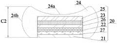
20-发光源;21-底座;22-P-GaN层;23-N-GaN层;24-微透镜;24a-第一出光面;24b-第二出光面;25-衬底层;26-MQWS层;27-焊盘;20-light source; 21-base; 22-P-GaN layer; 23-N-GaN layer; 24-microlens; 24a-first light-emitting surface; 24b-second light-emitting surface; 25-substrate layer; 26-MQWS layer; 27-pad;
30-基板。30 - Substrate.
具体实施方式Detailed ways
下面详细描述本发明的实施例,所述实施例的示例在附图中示出,其中自始至终相同或类似的标号表示相同或类似的元件或具有相同或类似功能的元件。下面通过参考附图描述的实施例是示例性的,仅用于解释本发明,而不能理解为对本发明的限制。The following describes in detail the embodiments of the present invention, examples of which are illustrated in the accompanying drawings, wherein the same or similar reference numerals refer to the same or similar elements or elements having the same or similar functions throughout. The embodiments described below with reference to the accompanying drawings are exemplary, only used to explain the present invention, and should not be construed as a limitation of the present invention.
在本发明的描述中,需要理解的是,术语“中心”、“纵向”、“横向”、“长度”、“宽度”、“厚度”、“上”、“下”、“前”、“后”、“左”、“右”、“竖直”、“水平”、“顶”、“底”、“内”、“外”、“顺时针”、“逆时针”、“轴向”、“径向”、“周向”等指示的方位或位置关系为基于附图所示的方位或位置关系,仅是为了便于描述本发明和简化描述,而不是指示或暗示所指的装置或元件必须具有特定的方位、以特定的方位构造和操作,因此不能理解为对本发明的限制。In the description of the present invention, it should be understood that the terms "center", "longitudinal", "lateral", "length", "width", "thickness", "upper", "lower", "front", " Back, Left, Right, Vertical, Horizontal, Top, Bottom, Inner, Outer, Clockwise, Counterclockwise, Axial , "radial", "circumferential" and other indicated orientations or positional relationships are based on the orientations or positional relationships shown in the accompanying drawings, and are only for the convenience of describing the present invention and simplifying the description, rather than indicating or implying the indicated device or Elements must have a particular orientation, be constructed and operate in a particular orientation and are therefore not to be construed as limitations of the invention.
此外,术语“第一”、“第二”仅用于描述目的,而不能理解为指示或暗示相对重要性或者隐含指明所指示的技术特征的数量。由此,限定有“第一”、“第二”的特征可以明示或者隐含地包括一个或者更多个该特征。在本发明的描述中,“多个”的含义是两个或两个以上,除非另有明确具体的限定。In addition, the terms "first" and "second" are only used for descriptive purposes, and should not be construed as indicating or implying relative importance or implying the number of indicated technical features. Thus, a feature defined as "first" or "second" may expressly or implicitly include one or more of that feature. In the description of the present invention, "plurality" means two or more, unless otherwise expressly and specifically defined.
在本发明中,除非另有明确的规定和限定,术语“安装”、“相连”、“连接”、“固定”等术语应做广义理解,例如,可以是固定连接,也可以是可拆卸连接,或成一体;可以是机械连接,也可以是电连接;可以是直接相连,也可以通过中间媒介间接相连,可以是两个元件内部的连通或两个元件的相互作用关系。对于本领域的普通技术人员而言,可以根据具体情况理解上述术语在本发明中的具体含义。In the present invention, unless otherwise expressly specified and limited, the terms "installed", "connected", "connected", "fixed" and other terms should be understood in a broad sense, for example, it may be a fixed connection or a detachable connection , or integrated; it can be a mechanical connection or an electrical connection; it can be a direct connection or an indirect connection through an intermediate medium, and it can be the internal connection of the two elements or the interaction relationship between the two elements. For those of ordinary skill in the art, the specific meanings of the above terms in the present invention can be understood according to specific situations.
在本发明中,除非另有明确的规定和限定,第一特征在第二特征“上”或“下”可以是第一和第二特征直接接触,或第一和第二特征通过中间媒介间接接触。而且,第一特征在第二特征“之上”、“上方”和“上面”可是第一特征在第二特征正上方或斜上方,或仅仅表示第一特征水平高度高于第二特征。第一特征在第二特征“之下”、“下方”和“下面”可以是第一特征在第二特征正下方或斜下方,或仅仅表示第一特征水平高度小于第二特征。In the present invention, unless otherwise expressly specified and limited, a first feature "on" or "under" a second feature may be in direct contact between the first and second features, or the first and second features indirectly through an intermediary touch. Also, the first feature being "above", "over" and "above" the second feature may mean that the first feature is directly above or obliquely above the second feature, or simply means that the first feature is level higher than the second feature. The first feature being "below", "below" and "below" the second feature may mean that the first feature is directly below or obliquely below the second feature, or simply means that the first feature has a lower level than the second feature.
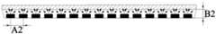
如图1所示,传统直下式LED电视的OD(Optical Distance,光程)大小B1一般在20-40mm,LED灯珠的间距A1在70-160mm,LED灯珠大小为3*3mm。传统直下式LED电视的背光源具有较少的LED灯珠数,但是仅能实现百枚以内的分区效果,无法满足现在所需求的高精密动态背光效果以及显示设备轻薄化的需求。As shown in Figure 1, the OD (Optical Distance, optical distance) size B1 of a traditional direct-type LED TV is generally 20-40mm, the spacing A1 of the LED lamp beads is 70-160mm, and the size of the LED lamp beads is 3*3mm. The backlight source of traditional direct-lit LED TVs has a small number of LED lamp beads, but can only achieve a partition effect of less than 100 pieces, which cannot meet the current demand for high-precision dynamic backlight effects and the need for thinner and lighter display devices.
随之,MINI LED灯珠(迷你灯珠)作为新的显示技术,具有体积小、厚度薄、毫米级像素分区等优点受到市场的青睐,使显示设备的OD大小B2可以控制在0.2-5mm。Subsequently, MINI LED lamp beads (mini lamp beads), as a new display technology, have the advantages of small size, thin thickness, and millimeter-level pixel division, which are favored by the market, so that the OD size B2 of the display device can be controlled within 0.2-5mm.
如图2和图3所示,现有的MINI LED灯珠都是采用COB(Chip on Board,芯片直接贴装技术)封装,LED芯片12直接倒装在线路板11上。由于COB封装工艺要求高,目前国内厂商还没有掌握其封装技术,因此在后期使用中不便于进行后期维修;当背光源出现单个MINILED灯珠坏掉时,则需要进行整板更换,从而增加了背光源的维修成本。As shown in FIG. 2 and FIG. 3 , the existing MINI LED lamp beads are all packaged by COB (Chip on Board, chip direct mounting technology), and the
且现有的MINI LED灯珠采用COB封装形势下,LED芯片12无支架直接倒装在线路板11上,LED芯片12高度D约为0.1mm,表面封装树脂13后MINI LED的高度C1约为0.25mm,树脂13无透镜结构。因此,现有的MINI LED灯珠基本上都是正面出光,侧面基本无光线射出,从而使背光源的灯珠之间光线能量较少;同时,由于现有的MINI LED灯珠高度较低,使混光距离不足;从而使MINI LED灯珠之间产生暗区。现有技术中为避免MINI LED灯珠之间出现暗区,需要将MINI LED灯珠进行密集排布,灯珠间距A2需要控制在3mm左右,需要在线路板11上布置大量的MINI LED灯珠,以65寸背光源为例就需要约十万颗MINI LED灯珠。从而,导致背光源成本增加、功率增加,且在工作时产生更多热量,影响背光源正常工作。In addition, when the existing MINI LED lamp beads are packaged by COB, the
实施例一Example 1
为解决上述技术问题,本发明提供了一种迷你灯珠,可实现侧面出光,增加灯珠间亮度,从而可以扩大灯珠间距,减小背光源上灯珠密度,进而降低成本及功耗。作为说明,实施例中,后文中出现的MINI LED灯珠即指所述的迷你灯珠。In order to solve the above technical problems, the present invention provides a mini lamp bead, which can realize side light emission and increase the brightness between the lamp beads, thereby expanding the lamp bead spacing, reducing the lamp bead density on the backlight source, and reducing cost and power consumption. As an illustration, in the embodiment, the MINI LED lamp beads appearing in the following text refer to the mini lamp beads.
如图4所示,所述MINI LED灯珠包括发光源20和微透镜24;所述微透镜24环绕罩设于所述发光源20上;所述微透镜24的下表面与所述发光源20的下表面齐平。如图4中所示的方向为基准定义上下左右等方位,上下左右等方位仅用于各部件相对位置的描述,不应作为对本申请的限制。As shown in FIG. 4 , the MINI LED lamp bead includes a light-emitting
所述微透镜24内设置有一容腔,所述发光源20设置于所述容腔内;所述容腔靠近微透镜24下表面的一侧具有开口端,所述发光源20的下表面通过所述开口端与外界接触。The
具体的,在生产加工过程中,将所述发光源20放入微透镜24的注塑模具中,随后向模具内浇筑微透镜24的制作原料,使微透镜24直接注塑在发光源20的外侧;同时,实现所述微透镜24与发光源20之间的固定连接。Specifically, during the production process, the light-emitting
所述发光源20产生的光线经过微透镜24后向外射出;所述微透镜24用于将所述发光源20产生的光线进行扩散,从而使MINI LED侧面也有光线射出,增加侧面出光。The light generated by the light-emitting
为了提高MINI LED灯珠的外量子效率,提高出光量,所述微透镜24可由具有高透射率和高耐光性的环氧树脂或硅树脂制成。In order to improve the external quantum efficiency of the MINI LED lamp beads and increase the light output, the
如图4和图5所示,所述微透镜24靠近所述发光源20的一面具有入光面,所述入光面与所述发光源20的侧面及上端面贴合设置;由此,所述发光源20的光线经过所述入光面进入所述微透镜24中。As shown in FIG. 4 and FIG. 5 , the side of the
所述微透镜24的外表面具有第一出光面24a和第二出光面24b,所述微透镜24内光线经过所述第一出光面24a和第二出光面24b向外射出。所述第一出光面24a对应所述发光源20的上方设置以实现部分光线向上透射,实现MINI LED灯珠的正面出光。所述第二出光面24b对应所述发光源20的侧面设置以使部分光线向MINI LED灯珠的侧面方向射出,从而实现MINI LED灯珠的侧面出光。The outer surface of the
在使用中,本申请的MINI LED灯珠通过增加侧面出光量,从而增加相邻MINI LED灯珠之间的光线能量,避免灯珠之间出现暗区。进而在背光源的生产加工中,可以减少MINILED灯珠数量的设置,降低背光源成本及功耗。In use, the MINI LED lamp beads of the present application increase the amount of light emitted from the side, thereby increasing the light energy between adjacent MINI LED lamp beads and avoiding dark areas between the lamp beads. Furthermore, in the production and processing of the backlight, the number of MINILED lamp beads can be reduced, and the cost and power consumption of the backlight can be reduced.
进一步,实施例中,所述第一出光面24a呈第一弧面结构,所述第一弧面结构向靠近所述发光源20上表面的方向凹陷。在所述第一出光面24a的边缘位置与中间位置之间的部分也呈现向内凹陷的弧面结构,使所述第一出光面24a呈现碗状结构。Further, in the embodiment, the first
从而,在使用中,发光源20的光线照射到所述第一出光面24a上时,部分光线会在第一出光面24a内侧发生全反射,反射到第二出光面24b,从第二出光面24b射出。Therefore, in use, when the light of the
具体的,由于微透镜24的介质密度大于空气的介质密度,即呈现光线从光密介质射向光疏介质中,当光线入射角大于临界角时会发生全反射。因此,在实施例中,靠近第一出光面24a边缘的光线入射角大于临界角,该部分光线会以全反射的形式射向第二出光面24b,由第二出光面24b向外射出。靠近第一出光面24a中间部位的光线入射角小于临界角,该部分光线通过第一出光面24a照射出去。从而,实现所述MINI LED灯珠的正面出光和侧面出光。Specifically, since the medium density of the
如图6所示,在另外一些实施例中,所述第一出光面24a的边缘位置与中间位置之间的部分呈现向外凸出的弧面结构,使所述第一出光面24a呈现类圆锥形结构。靠近第一出光面24a中间的光线入射角大于临界角,该部分光线会发生全反射照射到第二出光面24b,从第二出光面24b照射出去。靠近第一出光面24a边缘的光线入射角小于临界角,该部分光线从第一出光面24a射出去。从而,实现所述MINI LED灯珠的正面出光和侧面出光。As shown in FIG. 6 , in some other embodiments, the part between the edge position and the middle position of the first
所述第二出光面24b呈第二弧面结构,所述第二弧面结构向远离所述发光源20侧面的方向凸出设置。具体的,所述第二出光面24b由边缘位置向中间位置逐渐远离所述发光源20的侧面,从而尽量使照射到所述第二出光面24b上的光线入射角小于临界角,使照射到第二出光面24b上的光线透射出去。所述第二出光面24b与所述第一出光面24a的衔接处为弧面,以实现平滑过渡。The second
调节所述第一出光面24a和所述第二出光面24b的弧面参数,可以使发光源20产生的光线向第二出光面24b聚集并从第二出光面24b射出,从而实现减弱MINI LED灯珠正面出光,增强MINI LED灯珠侧面出光。本发明的MINI LED灯珠的发光角度可以达到±70°以上;进而在使用中,可以增加灯珠间距离,降低背光面中使用的MINI LED灯珠数量,降低成本。Adjusting the arc surface parameters of the first light-emitting
实施例中,所述发光源20包括底座21和LED芯片;所述LED芯片叠放在所述底座21的上方;所述LED芯片靠近所述第一出光面24a设置。In an embodiment, the light-emitting
本实施例中,所述底座21为MCPCB板(Metal Core PCB,金属基印刷电路板);所述LED芯片的电极靠近所述底座21一侧设置。所述底座21中对应所述LED芯片电极的位置设置有金属化过孔(图中未示出)。所述金属化过孔靠近LED芯片的一端通过焊盘27与所述LED芯片的电极连接,从而在使用中可实现电能传输。所述底座21远离所述LED芯片的一侧设置有两电极片,两所述电极片与LED芯片的电极一一对应;两所述电极片与底座21内对应的金属化过孔连接,实现电能传输;所述电极片用于与线路板电连接。所述底座21上的电极片之间的间距为0.5-1.0mm。In this embodiment, the base 21 is an MCPCB (Metal Core PCB, metal-based printed circuit board); the electrodes of the LED chip are disposed close to one side of the base 21 . A metallized via hole (not shown in the figure) is provided in the base 21 at a position corresponding to the electrode of the LED chip. One end of the metallized via hole close to the LED chip is connected to the electrode of the LED chip through the
在另外一些实施例中,所述底座21可以选用陶瓷底座;具体的,所述陶瓷底座可选用氧化铝陶瓷、氮化铝陶瓷、氧化铍陶瓷、碳化硅陶瓷或氮化硼陶瓷等。所述陶瓷底座内嵌设由金属导柱;所述陶瓷底座远离所述LED芯片的一侧设置有两电极片。所述金属导柱一端通过焊盘27与LED芯片的电极连接;所述金属导柱另一端与陶瓷底座上的电极片连接,从而实现电能传输。两所述电极片与LED芯片的两电极一一对应设置。In other embodiments, the base 21 can be selected from a ceramic base; specifically, the ceramic base can be selected from alumina ceramics, aluminum nitride ceramics, beryllium oxide ceramics, silicon carbide ceramics or boron nitride ceramics. Metal guide posts are embedded in the ceramic base; two electrode sheets are arranged on the side of the ceramic base away from the LED chip. One end of the metal guide post is connected to the electrode of the LED chip through the
在另外一些实施例中,所述陶瓷底座内还可通过设置金属化过孔等导电结构实现LED芯片电极与电极片之间的电连接,实现电能传输。In some other embodiments, the electrical connection between the LED chip electrode and the electrode sheet can also be realized by arranging conductive structures such as metallized via holes in the ceramic base to realize power transmission.
实施例中,所述LED芯片采用CSP(Chip Scale Package,芯片级封装)倒装制得,具有五面发光效果,即除了靠近所述底座21的一个面之外其它五个面都可以发出光线。所述底座21的设置相当于在LED芯片的下方加装了一托盘,拖住LED芯片的电极。所述底座21上的电极片之间的间距可以做到0.5-1.0mm,完全符合当前使用的SMT(Surface MountedTechnology,表面贴装技术)标准。从而,在进行背光源加工时,可以使用SMT工艺对MINILED灯珠进行贴装,由SMT机器抓取MINI LED灯珠放置在线路板上,再经过回流焊工艺将MINI LED灯珠固定在线路板上。In the embodiment, the LED chip is fabricated by flip-chip CSP (Chip Scale Package, chip scale package), and has a five-sided light-emitting effect, that is, except for one surface close to the base 21, the other five surfaces can emit light. . The setting of the base 21 is equivalent to adding a tray under the LED chip to drag the electrodes of the LED chip. The spacing between the electrode sheets on the base 21 can be 0.5-1.0 mm, which fully conforms to the currently used SMT (Surface Mounted Technology, surface mount technology) standard. Therefore, when processing the backlight source, the SMT process can be used to mount the MINI LED lamp beads, the SMT machine grabs the MINI LED lamp beads and places them on the circuit board, and then the MINI LED lamp beads are fixed on the circuit board through the reflow process. superior.
SMT工艺已经是较为成熟的技术,也是国内厂商较为常用的贴装技术;因此,在背光源的后期使用中,当出现单颗灯珠坏掉时,可直接对单颗灯珠进行维修,无需再进行整板替换维修,实现单颗溯源,进而降低了背光源的维修成本。The SMT process is already a relatively mature technology, and it is also a commonly used mounting technology by domestic manufacturers; therefore, in the later use of the backlight, when a single lamp bead is broken, the single lamp bead can be directly repaired without the need for Then the whole board is replaced and repaired to achieve single source traceability, thereby reducing the maintenance cost of the backlight.
所述底座21的设置,在MINI LED加工及贴装过程中,使CSP工艺与标准成熟的SMT工艺兼容,进而可以提高后期背光源的生产效率及良率,降低生产成本。The setting of the base 21 makes the CSP process compatible with the standard mature SMT process during the MINI LED processing and mounting process, thereby improving the production efficiency and yield of the backlight source in the later stage, and reducing the production cost.
同时,通过在LED芯片下方加装所述底座21使MINI LED灯珠的整体高度C2可以达到0.65mm,增加了光程距离,进而有助于光线MINI LED灯珠间进行混光效果,增加MINI LED灯珠间光线互补,进一步改善MINI LED灯珠间的光线效果,避免出现暗区。At the same time, by installing the base 21 under the LED chip, the overall height C2 of the MINI LED lamp beads can reach 0.65mm, which increases the optical path distance, which in turn helps the light mixing effect between the MINI LED lamp beads, and increases the MINI LED lamp beads. The light between the LED lamp beads is complementary to further improve the light effect between the MINI LED lamp beads and avoid dark areas.
如图4所示,实施例中,所述LED芯片包括依次叠放设置的外延层和衬底层25;所述外延层靠近所述底座21设置,所述衬底层25靠近第一出光面24a设置。所述LED芯片的电极刻蚀于所述外延层上。As shown in FIG. 4 , in the embodiment, the LED chip includes an epitaxial layer and a substrate layer 25 that are stacked in sequence; the epitaxial layer is disposed close to the base 21 , and the substrate layer 25 is disposed close to the first
所述外延层包括P-GaN层22(P型氮化镓)、MQWS层26(发光层)和N-GaN层23(N型氮化镓);所述MQWS层26设置于所述P-GaN层22和N-GaN层23之间。所述P-GaN层22靠近底座21设置;所述N-GaN层23靠近衬底层25设置。The epitaxial layer includes a P-GaN layer 22 (P-type gallium nitride), an MQWS layer 26 (light emitting layer) and an N-GaN layer 23 (N-type gallium nitride); the MQWS layer 26 is disposed on the P- between the GaN layer 22 and the N-GaN layer 23 . The P-GaN layer 22 is disposed close to the base 21 ; the N-GaN layer 23 is disposed close to the substrate layer 25 .
所述N-GaN层23、MQWS层26和P-GaN层22通过外延层生长法在所述衬底层25上依次生长制得。The N-GaN layer 23 , the MQWS layer 26 and the P-GaN layer 22 are sequentially grown on the substrate layer 25 by an epitaxial layer growth method.
本实施例中,所述衬底层25选用蓝宝石衬底(主要成分为氧化铝)。In this embodiment, the substrate layer 25 is a sapphire substrate (the main component is aluminum oxide).
在另外一些实施例中,所述衬底层25还可选用碳化硅衬底、硅衬底和氮化镓衬底。In other embodiments, the substrate layer 25 can also be selected from a silicon carbide substrate, a silicon substrate and a gallium nitride substrate.
综上,本申请提供的MINI LED灯珠经过微透镜24的设置,可以呈现±70°范围内的出光;同时,通过底座21的设置增加MINI LED灯珠的光程,改善MINI LED灯珠间的混光效果。从而,可以有效改善MINI LED灯珠间出现暗区的问题,有效拉大MINI LED灯珠间距离,MINI LED灯珠间距离可以由原有的3mm扩大到10mm左右。进而可以减少背光源加工中用到的MINI LED灯珠数量,单位面积内的可以节省十分之一的MINI LED灯珠数量,降低背光源的生产成本及功耗。To sum up, the MINI LED lamp beads provided in this application can present light in the range of ±70° through the setting of the
另外,通过底座21的设置使MINI LED灯珠的CSP封装技术与SMT贴装技术兼容;在背光源的加工过程中可直接通过SMT技术将MINI LED灯珠贴装在线路板上。从而,可以提高背光源的生产效率及良率,降低生产成本。同时,便于后期使用中的维修,实现单颗溯源维修,从而降低背光源的维修成本。In addition, through the setting of the base 21, the CSP packaging technology of the MINI LED lamp beads is compatible with the SMT mounting technology; during the processing of the backlight source, the MINI LED lamp beads can be directly mounted on the circuit board through the SMT technology. Therefore, the production efficiency and yield of the backlight can be improved, and the production cost can be reduced. At the same time, it is convenient for maintenance in later use, and single-chip traceability maintenance is realized, thereby reducing the maintenance cost of the backlight.
实施例二Embodiment 2
如图7所示,本实施例提供了一种背光源,包括基板30,所述基板30上呈阵列排布设置有所述的迷你灯珠(MINI LED灯珠);所述基板30即线路板。As shown in FIG. 7 , this embodiment provides a backlight, including a
所述MINI LED灯珠可以实现±70°的大角度发光范围,增加MINI LED灯珠间光线能量。同时,所述MINI LED灯珠高度C2在0.65mm左右,使MINI LED灯珠的具有较大的光程,从而增加了MINI LED灯珠间的混光效果。从而,本申请的背光源上的MINI LED灯珠间距离A3可以做到10mm左右,进而使基板30上的MINI LED灯珠密度可以减少,单位面积内本申请背光源中的MINI LED灯珠数量相较于传统背光源中的MINI LED灯珠数量可以减少十分之一。从而,本申请的背光源相较于传统的背光源具有较低的生产成本,及后期工作中具有较低的功耗。The MINI LED lamp beads can realize a large-angle light emission range of ±70°, and increase the light energy between the MINI LED lamp beads. At the same time, the height C2 of the MINI LED lamp bead is about 0.65mm, so that the MINI LED lamp bead has a larger light path, thereby increasing the light mixing effect between the MINI LED lamp bead. Therefore, the distance A3 between the MINI LED lamp beads on the backlight source of the present application can be about 10 mm, so that the density of the MINI LED lamp beads on the
实施例中,所述MINI LED灯珠通过成熟的SMT工艺贴装在基板30上。从而,当出现单颗MINI LED灯珠坏掉时,可进行单颗溯源,更换对应位置处的MINI LED灯珠即可,无需进行背光源的整板更换,进而降低背光源的后期维修成本。同时,通过SMT工艺对MINI LED灯珠进行贴装,可以提高背光源的生产效率及良率,以及降低背光源的生产成本。In the embodiment, the MINI LED lamp beads are mounted on the
实施例三
本实施例中提供了一种显示设备,包括显示面板、光学组件及所述的背光源。所述光学组件设置于所述显示面板和所述背光源之间。所述背光源产生的光线经过所述光学组件后照射在所述显示面板上,使显示面板成像。A display device is provided in this embodiment, including a display panel, an optical assembly and the aforementioned backlight. The optical assembly is disposed between the display panel and the backlight. The light generated by the backlight source passes through the optical assembly and then irradiates the display panel to image the display panel.
本申请的显示设备中,背光源上MINI LED灯珠的密度较小;在使用中,可以减小能耗及产热,从而确保背光源的正常工作,进而确保显示设备可以正常成像。In the display device of the present application, the density of the MINI LED lamp beads on the backlight source is small; in use, energy consumption and heat generation can be reduced, so as to ensure the normal operation of the backlight source, thereby ensuring that the display device can image normally.
实施例四Embodiment 4
如图8所示,本发明还提供了一种MINI LED灯珠的制作方法,用于制作所述的MINILED灯珠。所述制作方法包括:As shown in FIG. 8 , the present invention also provides a manufacturing method of a MINI LED lamp bead, which is used to manufacture the MINI LED lamp bead. The manufacturing method includes:
S100,将氧化铝粉末进行高温熔融形成液体,使种晶接触所述液体生成晶锭。具体的,将氧化铝粉末在2000℃的高温下进行融化成氧化铝液体;再将种晶与氧化铝液体接触,通过EFG(edge-defined,film-fed-growth)方法、Cz(czochralskr)方法或K(kyropoulos)方法生成晶锭。S100, the alumina powder is melted at a high temperature to form a liquid, and the seed crystal is brought into contact with the liquid to form an ingot. Specifically, the alumina powder is melted into an alumina liquid at a high temperature of 2000 °C; the seed crystal is then contacted with the alumina liquid, and the EFG (edge-defined, film-fed-growth) method, the Cz (czochralskr) method are used. Or K (kyropoulos) method to generate ingots.
S200,将所述晶锭进行切割、打磨以形成单晶晶片。具体的,将晶锭切割成单晶晶片,再经过研磨、抛光等工序去除单晶晶片表面的缺陷直至单晶晶片表面原子序列有序;所述缺陷包括单晶晶片表面的龟裂、破碎、缺陷或错位等。S200, cutting and grinding the ingot to form a single crystal wafer. Specifically, the ingot is cut into single crystal wafers, and then the defects on the surface of the single crystal wafer are removed through grinding, polishing and other processes until the atomic sequence of the surface of the single crystal wafer is ordered; the defects include cracks, cracks, Defects or dislocations, etc.
S300,通过外延生长结晶生长法在所述单晶晶片上生成外延层,形成外延晶元。具体的,通过外延生长法在单晶晶片表面依次生长出N-GaN层、MQWS层和P-GaN层。所述外延生长结晶生长法可选用LPE(liquid phase epitaxy)法、VPE(vapor phase epitaxy)法、OMVPE(metal-organic vapor phase epitaxy)法和MBE(molecular beam epitaxy)法中的一种。S300, an epitaxial layer is formed on the single crystal wafer by an epitaxial growth crystal growth method to form an epitaxial crystal. Specifically, an N-GaN layer, an MQWS layer and a P-GaN layer are sequentially grown on the surface of the single crystal wafer by an epitaxial growth method. The epitaxial crystal growth method can be selected from LPE (liquid phase epitaxy) method, VPE (vapor phase epitaxy) method, OMVPE (metal-organic vapor phase epitaxy) method and MBE (molecular beam epitaxy) method.
S400,在所述外延晶元的外延层制作电极,形成LED晶粒;在对外延晶元进行切割形成LED芯片。所述步骤S400具体包括:S400 , making electrodes on the epitaxial layer of the epitaxial wafer to form LED crystal grains; and cutting the epitaxial wafer to form LED chips. The step S400 specifically includes:
S401,形成晶粒,通过掩膜技术对发光部分进行覆盖形成掩膜;通过干式蚀刻法将无掩膜部分刻蚀掉,随后在去掉掩膜,使外延层上留下发光部位,形成多个发光二极管晶粒。S401 , forming crystal grains, and covering the light-emitting part by masking technology to form a mask; etching the non-masked part by dry etching, and then removing the mask to leave the light-emitting part on the epitaxial layer, forming a multi-layered a light-emitting diode die.
S402,制作透明电极,通过掩膜技术在非发光部位表面形成掩膜,通过真空蒸镀(或溅射镀膜)将透明电极材料覆盖在发光部位表面,形成p侧透明电极;随后去掉非发光部位的掩膜。S402, making a transparent electrode, forming a mask on the surface of the non-light-emitting part by masking technology, and covering the transparent electrode material on the surface of the light-emitting part by vacuum evaporation (or sputtering coating) to form a p-side transparent electrode; then removing the non-light-emitting part mask.
S403,制作电极板,通过掩膜技术在电极板位置处形成掩膜,再通过真空蒸镀在电极板位置处覆上电极材料,形成n侧电极板和p侧电极板,即LED芯片的电极;去掉掩膜。S403, making an electrode plate, forming a mask at the position of the electrode plate by masking technology, and then coating the electrode material at the position of the electrode plate by vacuum evaporation to form an n-side electrode plate and a p-side electrode plate, that is, the electrodes of the LED chip ; remove the mask.
S404,制作保护膜,在电极板形成后的晶元上利用溅射镀膜方法形成整体保护膜;再利用掩膜技术在非电极板部位形成掩膜;通过干式刻蚀法去掉电极板位置处的保护膜;去掉非电极板位置处的掩膜即可。S404 , a protective film is made, and a sputtering coating method is used to form an overall protective film on the wafer after the electrode plate is formed; a mask is then formed on the non-electrode plate position by using a mask technology; the electrode plate position is removed by dry etching the protective film; just remove the mask at the position of the non-electrode plate.
S405,以晶粒为单位将晶元进行分割,形成LED芯片。S405 , the wafer is divided in units of crystal grains to form LED chips.
S500,在所述LED芯片的电极板一侧加装底座。具体的,在LED芯片的电极板位置处设置焊盘,通过焊接将LED芯片的电极板、焊盘和底座之间进行固定连接,且可实现电能传输。S500, a base is installed on one side of the electrode plate of the LED chip. Specifically, a pad is arranged at the position of the electrode plate of the LED chip, and the electrode plate, the pad and the base of the LED chip are fixedly connected by welding, and power transmission can be realized.
S600,在加装底座的LED芯片上封装微透镜。具体的,将加装底座后的LED芯片放置到微透镜模具中;随后向模具中浇筑封装数值;再经过固化后脱模。所述固化包括前固化和后固化;其中,前固化是在135℃中维持一小时;后固化是对封装树脂进行热老化处理,在120℃下维持四小时。In S600, a microlens is packaged on an LED chip with a base. Specifically, the LED chip with the base added is placed in a microlens mold; then the package value is poured into the mold; and the mold is demolded after curing. The curing includes pre-curing and post-curing; wherein, the pre-curing is maintained at 135° C. for one hour; the post-curing is thermal aging treatment of the encapsulation resin, which is maintained at 120° C. for four hours.
其中,所述微透镜具有第一出光面和第二出光面;所述第一出光面对应所述LED芯片的上方一侧设置以使部分光线向上透射;所述第二出光面对应所述LED芯片的侧面设置以使部分光线向侧面透射。所述微透镜的设置使MINI LED灯珠的出光角度达到±70°,增大MINI LED灯珠侧面出光。从而在加工背光源时,可以减少MINI LED灯珠的密度,进而降低背光源的成本,以及后期使用中的功耗及产热。Wherein, the microlens has a first light-emitting surface and a second light-emitting surface; the first light-emitting surface is disposed corresponding to the upper side of the LED chip to transmit part of the light upward; the second light-emitting surface corresponds to the The side of the LED chip is arranged so that part of the light is transmitted to the side. The arrangement of the micro-lens enables the light-emitting angle of the MINI LED lamp beads to reach ±70°, which increases the light output from the side of the MINI LED lamp beads. Therefore, when processing the backlight, the density of the MINI LED lamp beads can be reduced, thereby reducing the cost of the backlight, as well as the power consumption and heat generation in later use.
同时,本发明制作的MINI LED灯珠可以符合成熟的SMT工艺标准,可直接通过SMT机器贴装在线路板上制作背光源,从而提高背光源的生产效率及良率,也便于后期的维修,降低背光源的维修维修成本。At the same time, the MINI LED lamp beads made by the present invention can meet the mature SMT process standard, and can be directly mounted on the circuit board through the SMT machine to make the backlight source, thereby improving the production efficiency and yield of the backlight source, and facilitating later maintenance. Reduce the maintenance and repair costs of the backlight.
在本说明书的描述中,参考术语“一个实施例”、“一些实施例”、“示例”、“具体示例”、或“一些示例”等的描述意指结合该实施例或示例描述的具体特征、结构、材料或者特点包含于本发明的至少一个实施例或示例中。在本说明书中,对上述术语的示意性表述不必须针对的是相同的实施例或示例。而且,描述的具体特征、结构、材料或者特点可以在任一个或多个实施例或示例中以合适的方式结合。此外,在不相互矛盾的情况下,本领域的技术人员可以将本说明书中描述的不同实施例或示例以及不同实施例或示例的特征进行结合和组合。In the description of this specification, description with reference to the terms "one embodiment," "some embodiments," "example," "specific example," or "some examples", etc., mean specific features described in connection with the embodiment or example , structure, material or feature is included in at least one embodiment or example of the present invention. In this specification, schematic representations of the above terms are not necessarily directed to the same embodiment or example. Furthermore, the particular features, structures, materials or characteristics described may be combined in any suitable manner in any one or more embodiments or examples. Furthermore, those skilled in the art may combine and combine the different embodiments or examples described in this specification, as well as the features of the different embodiments or examples, without conflicting each other.
尽管上面已经示出和描述了本发明的实施例,可以理解的是,上述实施例是示例性的,不能理解为对本发明的限制,本领域的普通技术人员在本发明的范围内可以对上述实施例进行变化、修改、替换和变型。Although the embodiments of the present invention have been shown and described above, it should be understood that the above-mentioned embodiments are exemplary and should not be construed as limiting the present invention. Embodiments are subject to variations, modifications, substitutions and variations.
Claims (10)
Priority Applications (2)
| Application Number | Priority Date | Filing Date | Title |
|---|---|---|---|
| CN202010256069.6ACN111312068A (en) | 2020-04-02 | 2020-04-02 | Mini lamp bead, manufacturing method, backlight source and display device |
| PCT/CN2020/125553WO2021196593A1 (en) | 2020-04-02 | 2020-10-30 | Mini lamp bead, fabrication method, backlight source and display device |
Applications Claiming Priority (1)
| Application Number | Priority Date | Filing Date | Title |
|---|---|---|---|
| CN202010256069.6ACN111312068A (en) | 2020-04-02 | 2020-04-02 | Mini lamp bead, manufacturing method, backlight source and display device |
Publications (1)
| Publication Number | Publication Date |
|---|---|
| CN111312068Atrue CN111312068A (en) | 2020-06-19 |
Family
ID=71162764
Family Applications (1)
| Application Number | Title | Priority Date | Filing Date |
|---|---|---|---|
| CN202010256069.6APendingCN111312068A (en) | 2020-04-02 | 2020-04-02 | Mini lamp bead, manufacturing method, backlight source and display device |
Country Status (2)
| Country | Link |
|---|---|
| CN (1) | CN111312068A (en) |
| WO (1) | WO2021196593A1 (en) |
Cited By (4)
| Publication number | Priority date | Publication date | Assignee | Title |
|---|---|---|---|---|
| CN112992877A (en)* | 2021-02-05 | 2021-06-18 | 业成科技(成都)有限公司 | Flip-chip light emitting diode, manufacturing method thereof and backlight module |
| CN113169258A (en)* | 2020-10-15 | 2021-07-23 | 泉州三安半导体科技有限公司 | Light emitting device |
| WO2021196593A1 (en)* | 2020-04-02 | 2021-10-07 | 深圳创维-Rgb电子有限公司 | Mini lamp bead, fabrication method, backlight source and display device |
| CN114913820A (en)* | 2022-05-11 | 2022-08-16 | 福建华佳彩有限公司 | Mini-LED partition design method |
Families Citing this family (2)
| Publication number | Priority date | Publication date | Assignee | Title |
|---|---|---|---|---|
| CN117691008B (en)* | 2023-12-12 | 2024-07-23 | 广东省旭晟半导体股份有限公司 | A method for manufacturing multi-faceted LED without molding |
| CN119300582B (en)* | 2024-12-03 | 2025-02-28 | 广东安林电子科技股份有限公司 | A SMD LED lamp bead |
Citations (11)
| Publication number | Priority date | Publication date | Assignee | Title |
|---|---|---|---|---|
| CN1831565A (en)* | 2005-03-08 | 2006-09-13 | 三星电子株式会社 | Lens, backlight assembly with the lens and liquid crystal display with the assembly |
| CN102141215A (en)* | 2010-01-28 | 2011-08-03 | 奇菱科技股份有限公司 | Light source device and backlight module comprising same |
| CN102460748A (en)* | 2009-06-09 | 2012-05-16 | 飞利浦拉米尔德斯照明设备有限责任公司 | Led with remote phosphor layer and reflective submount |
| CN204178089U (en)* | 2014-10-23 | 2015-02-25 | 晶科电子(广州)有限公司 | A kind of LED backlight and LED backlight module of exempting from secondary lens |
| CN206207081U (en)* | 2016-11-25 | 2017-05-31 | 欧普照明股份有限公司 | Light source module and lighting device |
| KR20170066753A (en)* | 2015-12-04 | 2017-06-15 | 엘지디스플레이 주식회사 | Light-Emitting Package for Display Device and Backlight Unit having the same |
| CN206291098U (en)* | 2016-12-29 | 2017-06-30 | 苏州欧普照明有限公司 | A kind of lens, light source module and lighting device |
| CN107044598A (en)* | 2017-02-07 | 2017-08-15 | 苏州欧普照明有限公司 | A kind of lens, light source module and lighting device |
| CN206741161U (en)* | 2017-05-22 | 2017-12-12 | 东莞市欧科光电科技有限公司 | A kind of LCDs LED lens |
| CN111552119A (en)* | 2020-06-02 | 2020-08-18 | 深圳创维-Rgb电子有限公司 | A lens film, light source assembly, backlight module and display device |
| CN211699541U (en)* | 2020-04-02 | 2020-10-16 | 深圳创维-Rgb电子有限公司 | Mini lamp bead, backlight and display device |
Family Cites Families (6)
| Publication number | Priority date | Publication date | Assignee | Title |
|---|---|---|---|---|
| CN101561587A (en)* | 2008-04-16 | 2009-10-21 | 中国科学院半导体研究所 | LED lens capable of being used for direct LCD backlight |
| JP2013218940A (en)* | 2012-04-11 | 2013-10-24 | Sharp Corp | Light-emitting module, lighting device including the same, and display device |
| JP6801695B2 (en)* | 2018-08-03 | 2020-12-16 | 日亜化学工業株式会社 | Light emitting module and its manufacturing method |
| CN208705619U (en)* | 2018-08-15 | 2019-04-05 | 广州视源电子科技股份有限公司 | Direct type backlight module structure and display equipment |
| CN110137162A (en)* | 2019-04-01 | 2019-08-16 | 深圳市瑞丰光电子股份有限公司 | An adjustable LED product and its manufacturing method |
| CN111312068A (en)* | 2020-04-02 | 2020-06-19 | 深圳创维-Rgb电子有限公司 | Mini lamp bead, manufacturing method, backlight source and display device |
- 2020
- 2020-04-02CNCN202010256069.6Apatent/CN111312068A/enactivePending
- 2020-10-30WOPCT/CN2020/125553patent/WO2021196593A1/ennot_activeCeased
Patent Citations (11)
| Publication number | Priority date | Publication date | Assignee | Title |
|---|---|---|---|---|
| CN1831565A (en)* | 2005-03-08 | 2006-09-13 | 三星电子株式会社 | Lens, backlight assembly with the lens and liquid crystal display with the assembly |
| CN102460748A (en)* | 2009-06-09 | 2012-05-16 | 飞利浦拉米尔德斯照明设备有限责任公司 | Led with remote phosphor layer and reflective submount |
| CN102141215A (en)* | 2010-01-28 | 2011-08-03 | 奇菱科技股份有限公司 | Light source device and backlight module comprising same |
| CN204178089U (en)* | 2014-10-23 | 2015-02-25 | 晶科电子(广州)有限公司 | A kind of LED backlight and LED backlight module of exempting from secondary lens |
| KR20170066753A (en)* | 2015-12-04 | 2017-06-15 | 엘지디스플레이 주식회사 | Light-Emitting Package for Display Device and Backlight Unit having the same |
| CN206207081U (en)* | 2016-11-25 | 2017-05-31 | 欧普照明股份有限公司 | Light source module and lighting device |
| CN206291098U (en)* | 2016-12-29 | 2017-06-30 | 苏州欧普照明有限公司 | A kind of lens, light source module and lighting device |
| CN107044598A (en)* | 2017-02-07 | 2017-08-15 | 苏州欧普照明有限公司 | A kind of lens, light source module and lighting device |
| CN206741161U (en)* | 2017-05-22 | 2017-12-12 | 东莞市欧科光电科技有限公司 | A kind of LCDs LED lens |
| CN211699541U (en)* | 2020-04-02 | 2020-10-16 | 深圳创维-Rgb电子有限公司 | Mini lamp bead, backlight and display device |
| CN111552119A (en)* | 2020-06-02 | 2020-08-18 | 深圳创维-Rgb电子有限公司 | A lens film, light source assembly, backlight module and display device |
Cited By (8)
| Publication number | Priority date | Publication date | Assignee | Title |
|---|---|---|---|---|
| WO2021196593A1 (en)* | 2020-04-02 | 2021-10-07 | 深圳创维-Rgb电子有限公司 | Mini lamp bead, fabrication method, backlight source and display device |
| CN113169258A (en)* | 2020-10-15 | 2021-07-23 | 泉州三安半导体科技有限公司 | Light emitting device |
| WO2022077368A1 (en)* | 2020-10-15 | 2022-04-21 | 泉州三安半导体科技有限公司 | Light emitting device |
| CN113169258B (en)* | 2020-10-15 | 2023-08-22 | 泉州三安半导体科技有限公司 | light emitting device |
| CN112992877A (en)* | 2021-02-05 | 2021-06-18 | 业成科技(成都)有限公司 | Flip-chip light emitting diode, manufacturing method thereof and backlight module |
| TWI765568B (en)* | 2021-02-05 | 2022-05-21 | 大陸商業成科技(成都)有限公司 | Flip-chip light-emitting diode, manufacturing method and backlight module therefor |
| CN112992877B (en)* | 2021-02-05 | 2022-11-22 | 业成科技(成都)有限公司 | Flip-chip light emitting diode, manufacturing method thereof and backlight module |
| CN114913820A (en)* | 2022-05-11 | 2022-08-16 | 福建华佳彩有限公司 | Mini-LED partition design method |
Also Published As
| Publication number | Publication date |
|---|---|
| WO2021196593A1 (en) | 2021-10-07 |
Similar Documents
| Publication | Publication Date | Title |
|---|---|---|
| CN111312068A (en) | Mini lamp bead, manufacturing method, backlight source and display device | |
| US9431592B2 (en) | Submount with cavities and through vias for LED packaging | |
| RU2617880C2 (en) | Moulded lens forming led-module of integrated circuit scale and manufacturing method thereof | |
| CN203774363U (en) | Semiconductor light-emitting device | |
| US7875897B2 (en) | Light emitting device | |
| CN104956500B (en) | Submountless light emitting diode (LED) component and method of making the same | |
| KR100845856B1 (en) | Light emitting device package and its manufacturing method | |
| US7732233B2 (en) | Method for making light emitting diode chip package | |
| TWI476946B (en) | Light-emitting diode device and method for fabricating the same | |
| US20140299898A1 (en) | Light emitting device module and method of manufacturing the same | |
| CN212257436U (en) | LED substrate, LED packaging body and display device | |
| TW201003986A (en) | Semiconductor device and method for fabricating the same | |
| TW200903865A (en) | Single crystal phosphor light conversion structures for light emitting devices | |
| CN109285932B (en) | Light emitting device package | |
| CN113054059A (en) | Display device, LED package and manufacturing method thereof | |
| CN106410022A (en) | Manufacturing method of LED packaging device and the LED packaging device | |
| CN100392855C (en) | U-groove LED integrated chip and manufacturing method | |
| JP5334123B2 (en) | Semiconductor light emitting device, semiconductor light emitting device assembly, and method of manufacturing semiconductor light emitting device | |
| CN109390449A (en) | Light emitting device package | |
| TW201042720A (en) | A wafer-level CSP processing method and thereof a thin-chip SMT-type light emitting diode | |
| JP2007214592A (en) | Light emitting device | |
| JP2008042149A (en) | High-current, high-efficiency surface-mount light-emitting diode lamp and method for manufacturing the same | |
| CN211699541U (en) | Mini lamp bead, backlight and display device | |
| CN101685783A (en) | Light emitting diode chip packaging structure and manufacturing method thereof | |
| CN101777549A (en) | Package module structure of compound semiconductor element and manufacturing method thereof |
Legal Events
| Date | Code | Title | Description |
|---|---|---|---|
| PB01 | Publication | ||
| PB01 | Publication | ||
| SE01 | Entry into force of request for substantive examination | ||
| SE01 | Entry into force of request for substantive examination |