CN111292632B - A display panel, glass assembly, dimming method and manufacturing method - Google Patents
A display panel, glass assembly, dimming method and manufacturing methodDownload PDFInfo
- Publication number
- CN111292632B CN111292632BCN202010097677.7ACN202010097677ACN111292632BCN 111292632 BCN111292632 BCN 111292632BCN 202010097677 ACN202010097677 ACN 202010097677ACN 111292632 BCN111292632 BCN 111292632B
- Authority
- CN
- China
- Prior art keywords
- liquid crystal
- transparent substrate
- dye liquid
- layer
- electroluminescent diode
- Prior art date
- Legal status (The legal status is an assumption and is not a legal conclusion. Google has not performed a legal analysis and makes no representation as to the accuracy of the status listed.)
- Active
Links
Images


Classifications
- G—PHYSICS
- G09—EDUCATION; CRYPTOGRAPHY; DISPLAY; ADVERTISING; SEALS
- G09F—DISPLAYING; ADVERTISING; SIGNS; LABELS OR NAME-PLATES; SEALS
- G09F9/00—Indicating arrangements for variable information in which the information is built-up on a support by selection or combination of individual elements
- G09F9/30—Indicating arrangements for variable information in which the information is built-up on a support by selection or combination of individual elements in which the desired character or characters are formed by combining individual elements
- G09F9/33—Indicating arrangements for variable information in which the information is built-up on a support by selection or combination of individual elements in which the desired character or characters are formed by combining individual elements being semiconductor devices, e.g. diodes
- G—PHYSICS
- G02—OPTICS
- G02F—OPTICAL DEVICES OR ARRANGEMENTS FOR THE CONTROL OF LIGHT BY MODIFICATION OF THE OPTICAL PROPERTIES OF THE MEDIA OF THE ELEMENTS INVOLVED THEREIN; NON-LINEAR OPTICS; FREQUENCY-CHANGING OF LIGHT; OPTICAL LOGIC ELEMENTS; OPTICAL ANALOGUE/DIGITAL CONVERTERS
- G02F1/00—Devices or arrangements for the control of the intensity, colour, phase, polarisation or direction of light arriving from an independent light source, e.g. switching, gating or modulating; Non-linear optics
- G02F1/01—Devices or arrangements for the control of the intensity, colour, phase, polarisation or direction of light arriving from an independent light source, e.g. switching, gating or modulating; Non-linear optics for the control of the intensity, phase, polarisation or colour
- G02F1/13—Devices or arrangements for the control of the intensity, colour, phase, polarisation or direction of light arriving from an independent light source, e.g. switching, gating or modulating; Non-linear optics for the control of the intensity, phase, polarisation or colour based on liquid crystals, e.g. single liquid crystal display cells
- G02F1/133—Constructional arrangements; Operation of liquid crystal cells; Circuit arrangements
- G02F1/13306—Circuit arrangements or driving methods for the control of single liquid crystal cells
- G—PHYSICS
- G02—OPTICS
- G02F—OPTICAL DEVICES OR ARRANGEMENTS FOR THE CONTROL OF LIGHT BY MODIFICATION OF THE OPTICAL PROPERTIES OF THE MEDIA OF THE ELEMENTS INVOLVED THEREIN; NON-LINEAR OPTICS; FREQUENCY-CHANGING OF LIGHT; OPTICAL LOGIC ELEMENTS; OPTICAL ANALOGUE/DIGITAL CONVERTERS
- G02F1/00—Devices or arrangements for the control of the intensity, colour, phase, polarisation or direction of light arriving from an independent light source, e.g. switching, gating or modulating; Non-linear optics
- G02F1/01—Devices or arrangements for the control of the intensity, colour, phase, polarisation or direction of light arriving from an independent light source, e.g. switching, gating or modulating; Non-linear optics for the control of the intensity, phase, polarisation or colour
- G02F1/13—Devices or arrangements for the control of the intensity, colour, phase, polarisation or direction of light arriving from an independent light source, e.g. switching, gating or modulating; Non-linear optics for the control of the intensity, phase, polarisation or colour based on liquid crystals, e.g. single liquid crystal display cells
- G02F1/133—Constructional arrangements; Operation of liquid crystal cells; Circuit arrangements
- G02F1/1333—Constructional arrangements; Manufacturing methods
- G02F1/1335—Structural association of cells with optical devices, e.g. polarisers or reflectors
Landscapes
- Physics & Mathematics (AREA)
- Nonlinear Science (AREA)
- General Physics & Mathematics (AREA)
- Mathematical Physics (AREA)
- Chemical & Material Sciences (AREA)
- Crystallography & Structural Chemistry (AREA)
- Optics & Photonics (AREA)
- Engineering & Computer Science (AREA)
- Theoretical Computer Science (AREA)
- Electroluminescent Light Sources (AREA)
- Devices For Indicating Variable Information By Combining Individual Elements (AREA)
Abstract
Translated fromChinese
Description
Translated fromChinese技术领域technical field
本发明涉及显示技术领域,特别是涉及一种显示面板、玻璃组件、调光方法和制作方法。The present invention relates to the field of display technology, in particular to a display panel, a glass assembly, a dimming method and a manufacturing method.
背景技术Background technique
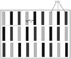
目前,现有商用车车窗的调光玻璃结构如图1所示,以乘用车的天窗为例,行业标准规定总成厚度最大为5mm,包括第一钢化玻璃1、第二钢化玻璃2、调光层3、调光层3分别通过第一PVB层4和第二PVB层5与第一钢化玻璃1和第二钢化玻璃2粘接,其中钢化玻璃和PVB为规格化产品,厚度已确定,分别为1.6mm和0.38mm,因此要求调光层厚度限定在1.04mm内,而现有技术中同时具有调光阵列和显示阵列的调光层的厚度远远超过该限定厚度,无法满足要求。同时,现有技术中调光阵列和显示阵列需要单独的阵列制程,对材料和工艺制作的成本需求较大,不利于产品的推广。另外,现有调光阵列通常采用负性液晶进行偏转,在制备调光阵列时需要涂覆PI配向膜,并采用Rubbing或光配向方式,使液晶形成一定预倾角,才能实现加电后液晶向特定方向偏转。At present, the dimming glass structure of the existing commercial vehicle window is shown in Figure 1. Taking the sunroof of a passenger car as an example, the industry standard stipulates that the maximum thickness of the assembly is 5mm, including the first
发明内容SUMMARY OF THE INVENTION
为了解决上述问题至少之一,本发明第一个实施例提供一种显示面板,包括In order to solve at least one of the above problems, a first embodiment of the present invention provides a display panel, comprising:
第一透明基板;a first transparent substrate;
第二透明基板;和a second transparent substrate; and
位于所述第一透明基板和第二透明基板之间的液晶盒,其中所述液晶盒包括依次层叠设置在所述第一透明基板上的电致发光二极管显示层、绝缘层和染料液晶层,其中a liquid crystal cell located between the first transparent substrate and the second transparent substrate, wherein the liquid crystal cell comprises an electroluminescent diode display layer, an insulating layer and a dye liquid crystal layer stacked on the first transparent substrate in sequence, in
所述电致发光二极管显示层,用于显示外部输入的待显示图像;The electroluminescent diode display layer is used to display an externally input image to be displayed;
所述染料液晶层,用于根据外部加载的电压透过或吸收外部入射光以呈现亮态或暗态。The dye liquid crystal layer is used for transmitting or absorbing external incident light according to an externally loaded voltage to present a bright state or a dark state.
进一步的,所述染料液晶层包括依次层叠设置在所述第二透明基板上的第一透明电极、染料液晶和第二透明电极,所述染料液晶响应于所述第一透明电极和第二透明电极上加载的电压发生偏转并透过或吸收外部入射光以呈现亮态或暗态。Further, the dye liquid crystal layer includes a first transparent electrode, a dye liquid crystal and a second transparent electrode stacked on the second transparent substrate in sequence, and the dye liquid crystal responds to the first transparent electrode and the second transparent electrode. The applied voltage on the electrodes is deflected and transmits or absorbs external incident light to exhibit a bright or dark state.
进一步的,所述电致发光二极管显示层包括设置在所述第一透明基板上的多个阵列排布的薄膜晶体管和由各所述薄膜晶体管驱动的电致发光二极管,其中Further, the electroluminescent diode display layer includes a plurality of thin film transistors arranged in an array on the first transparent substrate and electroluminescent diodes driven by each of the thin film transistors, wherein
所述薄膜晶体管包括有源层、栅极、源极和漏极;The thin film transistor includes an active layer, a gate electrode, a source electrode and a drain electrode;
所述电致发光二极管包括阳极、发光层和阴极,其中,所述阳极与所述源极和漏极中的一个电连接,并响应于外部输入到所述栅极的电信号接收外部输入到所述源极和漏极中的另一个的电信号;The electroluminescent diode includes an anode, a light-emitting layer, and a cathode, wherein the anode is electrically connected to one of the source and drain, and receives an external input to the gate in response to an electrical signal externally input to the gate. an electrical signal of the other of the source and drain;
所述电致发光二极管响应于外部输入到所述阳极和阴极的电信号显示所述待显示图像。The electroluminescent diode displays the to-be-displayed image in response to electrical signals externally input to the anode and cathode.
进一步的,所述电致发光二极管为条状结构,所述电致发光二极管的宽度与相邻两个所述电致发光二极管的间隙的比值小于预设宽度比。Further, the electroluminescent diode is a strip-shaped structure, and the ratio of the width of the electroluminescent diode to the gap between two adjacent electroluminescent diodes is smaller than a predetermined width ratio.
进一步的,所述第二透明电极为所述染料液晶层的公共电极、所述电致发光二极管位于所述薄膜晶体管远离所述第一透明基板的一侧、所述薄膜晶体管为顶栅结构并且所述电致发光二极管为底发射;Further, the second transparent electrode is the common electrode of the dye liquid crystal layer, the electroluminescent diode is located on the side of the thin film transistor away from the first transparent substrate, the thin film transistor has a top gate structure and The electroluminescent diode is bottom emission;
所述第二透明电极和所述电致发光二极管的阴极复用。The second transparent electrode is multiplexed with the cathode of the electroluminescent diode.
进一步的,所述染料液晶层的各染料液晶分子为宾主型染料液晶;Further, each dye liquid crystal molecule of the dye liquid crystal layer is a guest-host type dye liquid crystal;
和/或and / or
所述染料液晶层的各染料液晶分子为正性液晶或负性液晶。Each dye liquid crystal molecule of the dye liquid crystal layer is a positive liquid crystal or a negative liquid crystal.
本发明第二个实施例提供一种玻璃组件,包括第一个实施例所述的显示面板。A second embodiment of the present invention provides a glass assembly including the display panel described in the first embodiment.
本发明第三个实施例提供一种利用第一个实施例所述的显示面板的调光方法,包括:A third embodiment of the present invention provides a dimming method using the display panel described in the first embodiment, including:
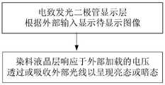
电致发光二极管显示层根据外部输入显示待显示图像;The electroluminescent diode display layer displays the image to be displayed according to the external input;
染料液晶层响应于外部加载的电压透过或吸收外部入射光以呈现亮态或暗态。The dye liquid crystal layer transmits or absorbs external incident light to exhibit a bright state or a dark state in response to an externally loaded voltage.
进一步的,further,
所述染料液晶层包括依次层叠设置在所述第二透明基板上的第一透明电极、染料液晶和第二透明电极;The dye liquid crystal layer includes a first transparent electrode, a dye liquid crystal and a second transparent electrode stacked on the second transparent substrate in sequence;
所述染料液晶层响应于外部加载的电压透过或吸收外部入射光以呈现亮态或暗态进一步包括:The dye liquid crystal layer transmitting or absorbing external incident light in response to an externally loaded voltage to exhibit a bright state or a dark state further includes:
所述染料液晶层响应于所述第一透明电极和第二透明电极加载的电压垂直于所述第一透明基板和第二透明基板,使得外部入射光透过所述染料液晶层以呈现亮态;The dye liquid crystal layer is perpendicular to the first transparent substrate and the second transparent substrate in response to the voltage loaded by the first transparent electrode and the second transparent electrode, so that external incident light passes through the dye liquid crystal layer to present a bright state ;
或者or
所述染料液晶层响应于所述第一透明电极和第二透明电极加载的电压水平于所述第一透明基板和第二透明基板,吸收所述外部入射光以呈现暗态。The dye liquid crystal layer absorbs the external incident light to exhibit a dark state in response to the voltage level loaded by the first transparent electrode and the second transparent electrode on the first transparent substrate and the second transparent substrate.
本发明第四个实施例提供一种制作第一个实施例所述显示面板的制作方法,包括:A fourth embodiment of the present invention provides a method for manufacturing the display panel described in the first embodiment, including:
在所述第一透明基板上形成电致发光二极管显示层;forming an electroluminescent diode display layer on the first transparent substrate;
在所述第二透明基板上形成染料液晶层;forming a dye liquid crystal layer on the second transparent substrate;
在所述电致发光二极管显示层和染料液晶层中的一个上形成绝缘层;forming an insulating layer on one of the electroluminescent diode display layer and the dye liquid crystal layer;
对盒所述第一透明基板和第二透明基板。The first transparent substrate and the second transparent substrate are assembled.
进一步的,further,
所述在所述第一透明基板上形成电致发光二极管显示层进一步包括:The forming an electroluminescent diode display layer on the first transparent substrate further includes:
在所述第一透明基板上形成多个阵列排布的薄膜晶体管;forming a plurality of thin film transistors arranged in an array on the first transparent substrate;
在所述薄膜晶体管上形成由各所述薄膜晶体管驱动的电致发光二极管;forming an electroluminescent diode driven by each of the thin film transistors on the thin film transistor;
和/或and / or
所述在所述第二透明基板上形成染料液晶层进一步包括:The forming the dye liquid crystal layer on the second transparent substrate further includes:
在所述第二透明基板上形成第一透明电极;forming a first transparent electrode on the second transparent substrate;
在所述第一透明电极上形成染料液晶;forming a dye liquid crystal on the first transparent electrode;
在所述染料液晶上形成第二透明电极。A second transparent electrode is formed on the dye liquid crystal.
本发明的有益效果如下:The beneficial effects of the present invention are as follows:
本发明针对目前现有的问题,制定一种显示面板、玻璃组件、调光方法和制作方法,通过集成在一个液晶盒中的电致发光二极管显示层和染料液晶层能够同时实现调光和显示功能,从而弥补了现有技术中存在的问题,并有效简化了制备工艺和制作成本,具有广泛的应用前景。Aiming at the existing problems at present, the present invention formulates a display panel, a glass component, a dimming method and a manufacturing method, which can realize dimming and display at the same time through the electroluminescent diode display layer and the dye liquid crystal layer integrated in a liquid crystal cell function, thereby making up for the problems existing in the prior art, and effectively simplifying the preparation process and production cost, and has broad application prospects.
附图说明Description of drawings
为了更清楚地说明本发明实施例中的技术方案,下面将对实施例描述中所需要使用的附图作简单地介绍,显而易见地,下面描述中的附图仅仅是本发明的一些实施例,对于本领域普通技术人员来讲,在不付出创造性劳动的前提下,还可以根据这些附图获得其他的附图。In order to illustrate the technical solutions in the embodiments of the present invention more clearly, the following briefly introduces the accompanying drawings used in the description of the embodiments. Obviously, the accompanying drawings in the following description are only some embodiments of the present invention. For those of ordinary skill in the art, other drawings can also be obtained from these drawings without creative effort.
图1示出现有技术中调光玻璃的结构示意图;Fig. 1 shows the structural schematic diagram of the dimming glass in the prior art;
图2示出本发明的一个实施例所述显示面板的层结构图;FIG. 2 shows a layer structure diagram of a display panel according to an embodiment of the present invention;
图3示出本发明的一个实施例所述显示面板的结构示意图;FIG. 3 shows a schematic structural diagram of a display panel according to an embodiment of the present invention;
图4示出本发明的一个实施例所述电致发光二极管显示层的电致发光二极管的分布示意图;FIG. 4 shows a schematic diagram of the distribution of the electroluminescent diodes of the electroluminescent diode display layer according to an embodiment of the present invention;
图5示出本发明的另一个实施例所述显示面板的层结构图;FIG. 5 shows a layer structure diagram of a display panel according to another embodiment of the present invention;
图6示出本发明的另一个实施例所述显示面板的驱动电路的示意图;FIG. 6 shows a schematic diagram of a driving circuit of a display panel according to another embodiment of the present invention;
图7a-7d示出本发明的另一个实施例所述显示面板的各状态示意图;7a-7d show schematic diagrams of various states of the display panel according to another embodiment of the present invention;
图8示出本发明的一个实施例所述调光方法的流程图;FIG. 8 shows a flowchart of the dimming method according to an embodiment of the present invention;
图9示出本发明的一个实施例所述制作方法的流程图。FIG. 9 shows a flow chart of a manufacturing method according to an embodiment of the present invention.
具体实施方式Detailed ways
为了更清楚地说明本发明,下面结合优选实施例和附图对本发明做进一步的说明。附图中相似的部件以相同的附图标记进行表示。本领域技术人员应当理解,下面所具体描述的内容是说明性的而非限制性的,不应以此限制本发明的保护范围。In order to illustrate the present invention more clearly, the present invention will be further described below with reference to the preferred embodiments and accompanying drawings. Similar parts in the figures are denoted by the same reference numerals. Those skilled in the art should understand that the content specifically described below is illustrative rather than restrictive, and should not limit the protection scope of the present invention.
需要说明的是,本文中所述的“在……上”、“在……上形成”和“设置在……上”可以表示一层直接形成或设置在另一层上,也可以表示一层间接形成或设置在另一层上,即两层之间还存在其它的层。在本文中,除非另有说明,所采用的术语“位于同一层”指的是两个层、部件、构件、元件或部分可以通过同一构图工艺形成,并且,这两个层、部件、构件、元件或部分一般由相同的材料形成。在本文中,除非另有说明,表述“构图工艺”一般包括光刻胶的涂布、曝光、显影、刻蚀、光刻胶的剥离等步骤。表述“一次构图工艺”意指使用一块掩模板形成图案化的层、部件、构件等的工艺。It should be noted that "on", "formed on" and "disposed on" described herein may mean that one layer is directly formed or disposed on another layer, or may mean that a layer is formed directly on or disposed on another layer. A layer is formed or disposed indirectly on another layer, ie there are other layers in between. As used herein, unless otherwise specified, the term "on the same layer" means that two layers, parts, members, elements or sections may be formed by the same patterning process, and that the two layers, parts, members, The elements or parts are generally formed from the same material. In this document, unless otherwise specified, the expression "patterning process" generally includes steps of photoresist coating, exposure, development, etching, and photoresist stripping. The expression "one-shot patterning process" means a process of forming patterned layers, features, members, etc. using one mask.
如图2所示,本发明的一个实施例提供了一种显示面板,包括第一透明基板11;第二透明基板12;和位于所述第一透明基板11和第二透明基板12之间的液晶盒,其中所述液晶盒包括依次层叠设置在所述第一透明基板11上的电致发光二极管显示层13、绝缘层14和染料液晶层15,其中所述电致发光二极管显示层13,用于显示外部输入的待显示图像;所述染料液晶层15,用于根据外部加载的电压透过或吸收外部入射光以呈现亮态或暗态。As shown in FIG. 2 , an embodiment of the present invention provides a display panel including a first
在本实施例中,将用于调光功能的染料液晶层和用于显示功能的电致发光二极管显示层通过封框胶16集成在一个液晶盒内,有效降低了现有技术中使用两个独立并且层叠设置的调光阵列和显示阵列的厚度,同时通过一个阵列制程完成所述显示面板的制备,有效降低了材料和工艺制作成本的需求。In this embodiment, the dye liquid crystal layer for the dimming function and the electroluminescent diode display layer for the display function are integrated into one liquid crystal cell through the
在一个可选的实施例中,如图2所示,所述染料液晶层15包括依次层叠设置在所述第二透明基板12上的第一透明电极151、染料液晶152和第二透明电极153,所述染料液晶152响应于所述第一透明电极151和第二透明电极153上加载的电压发生偏转并透过或吸收外部入射光以呈现亮态或暗态。In an optional embodiment, as shown in FIG. 2 , the dye
在一个具体的示例中,如图2所示,所述染料液晶层15的各染料液晶分子响应于第一透明电极151和第二透明电极153上加载的电压发生偏转,从而吸收外部入射光以实现暗态显示,或者不吸收外部入射光使得外部入射光透过染料液晶层以实现亮态显示。In a specific example, as shown in FIG. 2 , each dye liquid crystal molecule of the dye
其中,所述染料液晶为宾主型染料液晶,即在液晶分子中掺杂二向色性染料形成。具体的,在液晶中溶解二向色性染料即构成一种液晶分子为主、二向色性染料分子为宾的宾主型染料液晶。二向色性染料具有对光选择性吸收的特性,因此,可以通过液晶分子来诱导二向色性染料分子的排列,从而控制光的通过。在本实施例中,所述染料液晶层的各染料液晶分子为负性液晶,当不向第一透明电极151和第二透明电极153加载电压时,各液晶分子垂直于所述第一透明基板和第二透明基板,所述染料分子不吸收外部入射光,则外部入射光透过所述染料液晶层呈现亮态;当向第一透明电极151和第二透明电极153加载电压并形成电场,在电场作用下,各染料液晶分子发生偏转,则各染料液晶分子中的染料分子随着液晶分子转动并平行于所述第一透明基板和第二透明基板,外部入射光被染料分子吸收呈现暗态;从而实现染料液晶层的亮态和暗态的切换。Wherein, the dye liquid crystal is a guest-host type dye liquid crystal, that is, a liquid crystal molecule is formed by doping a dichroic dye. Specifically, dissolving the dichroic dye in the liquid crystal constitutes a guest-host dye liquid crystal in which the liquid crystal molecules are the main molecules and the dichroic dye molecules are the guest. Dichroic dyes have the characteristic of selectively absorbing light. Therefore, the arrangement of dichroic dye molecules can be induced by liquid crystal molecules, thereby controlling the passage of light. In this embodiment, each dye liquid crystal molecule of the dye liquid crystal layer is a negative liquid crystal. When no voltage is applied to the first
需要注意的是,本申请对染料液晶层的液晶分子不做具体限定,可以为正性液晶也可以为负性液晶,本领域技术人员应当根据实际应用需求选择适当的液晶分子。It should be noted that the application does not specifically limit the liquid crystal molecules of the dye liquid crystal layer, which can be either positive liquid crystals or negative liquid crystals. Those skilled in the art should select appropriate liquid crystal molecules according to practical application requirements.
在一个可选的实施例中,如图2所示,所述电致发光二极管显示层13包括设置在所述第一透明基板11上的多个阵列排布的薄膜晶体管131和由各所述薄膜晶体管131驱动的电致发光二极管132,其中所述薄膜晶体管131包括有源层、栅极、源极和漏极;所述电致发光二极管132包括阳极、发光层和阴极133,其中,所述阳极与所述源极和漏极中的一个电连接,并响应于外部输入到所述栅极的电信号接收外部输入到所述源极和漏极中的另一个的电信号;所述电致发光二极管132响应于外部输入到所述阳极和阴极133的电信号显示所述待显示图像。In an optional embodiment, as shown in FIG. 2 , the electroluminescent
在本实施例中,如图3所示,所述电致发光二极管响应于阳极和阴极加载的电信号进行显示,具体的,所述薄膜晶体管131形成在第一透明基板11上,包括有源层136、栅极137、源极138和漏极139,所述薄膜晶体管131响应于外部输入到栅极137的栅极信号导通所述源极138和漏极139,将所述源极138电连接的外部电信号传输至所述漏极139。所述电致发光二极管132包括阳极135、发光层134和阴极133,其中,所述阳极135通过过孔与所述漏极139电连接,当所述薄膜晶体管131导通时接收所述漏极传输的电信号;所述电致发光二极管132的发光层134响应于所述阳极135和阴极133上加载的电压发光,即所述电致发光二极管响应于外部输入到所述阳极和阴极的电信号显示所述待显示图像。In this embodiment, as shown in FIG. 3 , the electroluminescent diode displays in response to the electrical signals loaded by the anode and the cathode. Specifically, the
值得注意的时,在本实施例中,尽管所述电致发光二极管显示层13与所述染料液晶层15设置在同一个液晶盒中,所述电致发光二极管显示层13与所述染料液晶层15均为独立控制器件,即所述显示面板的调光功能和显示功能独立运行。It should be noted that, in this embodiment, although the electroluminescent
考虑到显示面板的调光性能,在一个可选的实施例中,如图4所示,所述电致发光二极管132为条状结构,所述电致发光二极管的宽度m1与相邻两个所述电致发光二极管的间隙m2的比值小于预设宽度比。Considering the dimming performance of the display panel, in an optional embodiment, as shown in FIG. 4 , the
在本实施例中,所述显示面板的电致发光二极管显示层的每个像素包括三个子像素,分别为红绿蓝三个子像素,所述各子像素为条状结构,并且各子像素之间具有一定的间隙。当所述染料液晶层15呈现亮态时从染料液晶层透射的外部入射光不仅作为各子像素的背景光,还从各子像素之间的间隙透过,当所述染料液晶层15呈现暗态时为所述电致发光二极管显示层提供暗态背景。当所述像素的宽度一定时,所述间隙越大则外部入射光的透过率越高;即所述电致发光二极管的宽度m1与相邻两个所述电致发光二极管的间隙m2的宽度比,与所述显示面板的整体亮态透过率成反比例关系。在本实施例中,当所述电致发光二极管的宽度m1与相邻两个所述电致发光二极管的间隙m2的宽度比的比值小于2:3时,所述显示面板的整体亮态透过率高于40%。In this embodiment, each pixel of the electroluminescent diode display layer of the display panel includes three sub-pixels, three sub-pixels of red, green and blue, each of the sub-pixels has a stripe structure, and the There is a certain gap between them. When the dye
同时,如图3所示,由于电致发光二极管显示层中相邻两个电致发光二极管间存在较大的间隙,所述电致发光二极管的膜层高于间隙位置的膜层,即所述电致发光二极管在基板表面呈现为突起状结构,使得染料液晶层中位于所述电致发光二极管附近的染料液晶分子并非完全垂直于第一透明基板和第二透明基板,而是在垂直于第一透明基板和第二透明基板的方向上发生一定倾斜,从而实现特定方向的预取向。由于该预取向的存在,当向第一透明电极和第二透明电极加载电压时,已预取向染料液晶分子会沿倾斜方向偏转,并带动其他染料液晶分子向垂直像素方向偏转,最终实现所有染料液晶分子的全部偏转,从而无需对PI进行配向,有效降低工艺复杂程度。At the same time, as shown in FIG. 3 , since there is a large gap between two adjacent electroluminescent diodes in the electroluminescent diode display layer, the film layer of the electroluminescent diode is higher than the film layer at the gap position, that is, the The electroluminescent diode exhibits a protruding structure on the surface of the substrate, so that the dye liquid crystal molecules in the dye liquid crystal layer near the electroluminescent diode are not completely perpendicular to the first transparent substrate and the second transparent substrate, but are perpendicular to the A certain inclination occurs in the directions of the first transparent substrate and the second transparent substrate, so as to achieve pre-orientation in a specific direction. Due to the existence of the pre-alignment, when a voltage is applied to the first transparent electrode and the second transparent electrode, the pre-aligned dye liquid crystal molecules will be deflected in the oblique direction, and will drive other dye liquid crystal molecules to be deflected in the direction vertical to the pixel, and finally all dyes will be realized. The liquid crystal molecules are all deflected, so that the PI does not need to be aligned, and the complexity of the process is effectively reduced.
值得说明的是,本申请对电致发光二极管显示层的结构不做限定,对所述染料液晶层的结构也不做限定,本领域技术人员应当根据实际应用需求设置所述电致发光二极管显示层和所述染料液晶层的具体结构,例如电极结构、发光方向和薄膜晶体管的结构等等,以实现独立的调光功能和显示功能为设计准则,在此不再赘述。It is worth noting that this application does not limit the structure of the electroluminescent diode display layer, nor does it limit the structure of the dye liquid crystal layer. Those skilled in the art should set the electroluminescent diode display according to actual application requirements. The specific structure of the layer and the dye liquid crystal layer, such as the electrode structure, the light-emitting direction and the structure of the thin film transistor, etc., are designed to achieve independent dimming function and display function, and will not be repeated here.
考虑到进一步简化显示面板的结构,在一个可选的实施例中,如图5所示,所述第二透明电极153为所述染料液晶层15的公共电极、所述电致发光二极管132位于所述薄膜晶体管131远离所述第一透明基板11的一侧、所述薄膜晶体管131为顶栅结构并且所述电致发光二极管132为底发射;所述第二透明电极153和所述电致发光二极管132的阴极133复用。In order to further simplify the structure of the display panel, in an optional embodiment, as shown in FIG. 5 , the second
在本实施例中,如图6所示,所述驱动电路利用所述染料液晶层的两个透明电极中的一个是公共电极,并且所述电致发光二极管显示层的各电致发光二极管的阴极也为公共电极,因此将所述染料液晶层和电致发光二极管显示层的结构进行限定,其中,所述染料液晶层的第一透明电极为像素电极并且第二透明电极为公共电极,所述电致发光二极管显示层的薄膜晶体管为顶栅结构以便于连接外部输入的电信号,并且各所述电致发光二极管为底发射,此时染料液晶层的公共电极和电致发光二极管的阴极复用。具体的,图6为所述显示面板的驱动电路的等效电路图,从图中可知,VLC为染料液晶驱动电压,为0~24V交流信号,Vcom为公共电极,各染料液晶分子响应于VLC和Vcom加载电压形成的电场进行偏转;同时,电致发光二极管OLED采用一个薄膜晶体管进行控制,Vgate为薄膜晶体管的开关电压,Vdata为直流信号,薄膜晶体管响应于Vgate导通并将Vdata传输至电致发光二极管OLED的阳极,电致发光二极管OLED响应于Vdata和Vcom加载的电压发光。本实施例有效简化显示面板的膜层结构,同时减少制作工艺流程并降低所述显示面板的制作成本。In this embodiment, as shown in FIG. 6 , the driving circuit uses one of the two transparent electrodes of the dye liquid crystal layer as a common electrode, and the electroluminescent diodes of the electroluminescent diode display layer have The cathode is also the common electrode, so the structures of the dye liquid crystal layer and the electroluminescent diode display layer are defined, wherein the first transparent electrode of the dye liquid crystal layer is the pixel electrode and the second transparent electrode is the common electrode, so The thin film transistor of the electroluminescent diode display layer has a top-gate structure so as to be connected to externally input electrical signals, and each electroluminescent diode is bottom-emitting. At this time, the common electrode of the dye liquid crystal layer and the cathode of the electroluminescent diode are reuse. Specifically, FIG. 6 is an equivalent circuit diagram of the driving circuit of the display panel. It can be seen from the figure that VLC is the driving voltage of the dye liquid crystal, which is an AC signal of 0-24V, and Vcom is the common electrode. Each dye liquid crystal molecule responds to The electric field formed by the loading voltage of VLC and Vcom is deflected; at the same time, the electroluminescent diode OLED is controlled by a thin film transistor, Vgate is the switching voltage of the thin film transistor, Vdata is the DC signal, and the thin film transistor is turned on in response to Vgate and transmitsVdata to the anode of the electroluminescent diode OLED, which emits light in response to the applied voltages ofVdata andVcom . This embodiment effectively simplifies the film layer structure of the display panel, reduces the manufacturing process flow and reduces the manufacturing cost of the display panel.
在本实施例中,如图7a-7d所示,通过独立控制所述电致发光二极管显示层和所述染料液晶层,能够同时实现调光功能和显示功能。具体的,如图7a所示,当所述染料液晶层为亮态(各染料液晶分子垂直于所述第一透明基板和第二透明基板)并且所述电致发光二极管显示层进行显示(各电致发光二极管发光)时,所述显示面板呈现以外部入射光为背景的显示图像;如图7b所示,当所述染料液晶层为暗态并且所述电致发光二极管显示层进行显示时,所述显示面板呈现以暗态背景为背景的显示图像;如图7c所示,当所述染料液晶层为亮态并且所述电致发光二极管显示层不进行显示时,所述显示面板呈现为外部入射光;如图7d所示,当所述染料液晶层为暗态并且所述电致发光二极管显示层不进行显示时,所述显示面板呈现为暗态背景。In this embodiment, as shown in FIGS. 7a-7d, by independently controlling the electroluminescent diode display layer and the dye liquid crystal layer, the dimming function and the display function can be simultaneously realized. Specifically, as shown in FIG. 7a, when the dye liquid crystal layer is in a bright state (each dye liquid crystal molecule is perpendicular to the first transparent substrate and the second transparent substrate) and the electroluminescent diode display layer displays (each dye liquid crystal molecule is perpendicular to the first transparent substrate and the second transparent substrate) When the electroluminescent diode emits light), the display panel presents a display image with external incident light as the background; as shown in FIG. 7b, when the dye liquid crystal layer is in a dark state and the electroluminescent diode display layer is displaying , the display panel presents a display image with a dark state background as the background; as shown in FIG. 7c, when the dye liquid crystal layer is in a bright state and the electroluminescent diode display layer does not display, the display panel presents is external incident light; as shown in FIG. 7d , when the dye liquid crystal layer is in a dark state and the electroluminescent diode display layer does not display, the display panel presents a dark state background.
与上述实施例提供的显示面板相对应,本申请的一个实施例还提供一种利用上述显示面板的调光方法,由于本申请实施例提供的调光方法与上述几种实施例提供的显示面板相对应,因此在前实施方式也适用于本实施例提供的调光方法,在本实施例中不再详细描述。Corresponding to the display panel provided by the above-mentioned embodiment, an embodiment of the present application further provides a dimming method using the above-mentioned display panel. Correspondingly, therefore, the previous implementation manner is also applicable to the dimming method provided in this embodiment, which will not be described in detail in this embodiment.
如图8所示,本发明的一个实施例提供了一种利用上述显示面板的调光方法,包括:电致发光二极管显示层根据外部输入显示待显示图像;染料液晶层响应于外部加载的电压透过或吸收外部入射光以呈现亮态或暗态。As shown in FIG. 8 , an embodiment of the present invention provides a dimming method using the above-mentioned display panel, including: an electroluminescent diode display layer displays an image to be displayed according to an external input; a dye liquid crystal layer responds to an externally loaded voltage Transmits or absorbs external incident light to present a bright or dark state.
在本实施例中,所述显示面板通过电致发光二极管显示层进行显示,通过染料液晶层透过外部入射光或阻挡外部入射光从而实现亮态或暗态。In this embodiment, the display panel is displayed through an electroluminescent diode display layer, and the dye liquid crystal layer transmits or blocks external incident light to achieve a bright state or a dark state.
在一个可选的实施例中,所述染料液晶层包括依次层叠设置在所述第二透明基板上的第一透明电极、染料液晶和第二透明电极;所述染料液晶层响应于外部加载的电压透过或吸收外部入射光以呈现亮态或暗态进一步包括:所述染料液晶层响应于所述第一透明电极和第二透明电极加载的电压垂直于所述第一透明基板和第二透明基板,使得外部入射光透过所述染料液晶层以呈现亮态;或者所述染料液晶层响应于所述第一透明电极和第二透明电极加载的电压水平于所述第一透明基板和第二透明基板,吸收所述外部入射光以呈现暗态。In an optional embodiment, the dye liquid crystal layer includes a first transparent electrode, a dye liquid crystal and a second transparent electrode sequentially stacked on the second transparent substrate; the dye liquid crystal layer responds to externally loaded Transmitting or absorbing external incident light with a voltage to present a bright state or a dark state further comprises: the dye liquid crystal layer is perpendicular to the first transparent substrate and the second transparent electrode in response to the voltage applied by the first transparent electrode and the second transparent electrode a transparent substrate, so that external incident light passes through the dye liquid crystal layer to present a bright state; or the dye liquid crystal layer responds to the voltage level loaded by the first transparent electrode and the second transparent electrode to the first transparent substrate and the second transparent electrode. The second transparent substrate absorbs the external incident light to present a dark state.
在本实施例中,通过控制加载在所述染料液晶层的第一透明基板和第二透明基板上的电压控制各染料液晶分子的偏转方向:当各染料液晶分子垂直于第一透明基板和第二透明基板,外部入射光不被染料液晶分子吸收,即外部入射光透过所述染料液晶层呈现为亮态;当各染料液晶分子水平于第一透明基板和第二透明基板,外部入射光被染料液晶分子吸收,即外部入射光未透过所述染料液晶层呈现为暗态。In this embodiment, the deflection direction of each dye liquid crystal molecule is controlled by controlling the voltage loaded on the first transparent substrate and the second transparent substrate of the dye liquid crystal layer: when each dye liquid crystal molecule is perpendicular to the first transparent substrate and the second transparent substrate Two transparent substrates, the external incident light is not absorbed by the dye liquid crystal molecules, that is, the external incident light passes through the dye liquid crystal layer to present a bright state; when each dye liquid crystal molecule is horizontal to the first transparent substrate and the second transparent substrate, the external incident light Absorbed by the dye liquid crystal molecules, that is, the external incident light does not pass through the dye liquid crystal layer and appears as a dark state.
具体的,当所述染料液晶层的各染料液晶分子为负性液晶,利用负性液晶在未加电场时垂直于第一透明基板和第二透明基板的特性,当需要呈现亮态时不向第一透明电极和第二透明电极加载电压,则各染料液晶分子保持垂直于第一透明基板和第二透明基板的状态,外部入射光透过所述染料液晶层;当需要呈现暗态时向第一透明电极和第二透明电极加载电压则各染料液晶分子发生偏转并水平于第一透明基板和第二透明基板,所述各染料液晶分子吸收外部入射光,阻挡外部入射光透过所述染料液晶层。Specifically, when each dye liquid crystal molecule of the dye liquid crystal layer is a negative liquid crystal, the negative liquid crystal is perpendicular to the first transparent substrate and the second transparent substrate when no electric field is applied, and when it needs to be in a bright state, it is not directed toward the When voltage is applied to the first transparent electrode and the second transparent electrode, each dye liquid crystal molecule maintains a state perpendicular to the first transparent substrate and the second transparent substrate, and external incident light passes through the dye liquid crystal layer; When the voltage is applied to the first transparent electrode and the second transparent electrode, the dye liquid crystal molecules are deflected and are horizontal to the first transparent substrate and the second transparent substrate. The dye liquid crystal molecules absorb external incident light and block external incident light from passing through the Dye liquid crystal layer.
如图9所示,本发明的一个实施例提供了一种制作上述显示面板的制作方法,包括:在所述第一透明基板上形成电致发光二极管显示层;在所述第二透明基板上形成染料液晶层;在所述电致发光二极管显示层和染料液晶层中的一个上形成绝缘层;对盒所述第一透明基板和第二透明基板。As shown in FIG. 9 , an embodiment of the present invention provides a manufacturing method for the above-mentioned display panel, which includes: forming an electroluminescent diode display layer on the first transparent substrate; forming an electroluminescent diode display layer on the second transparent substrate; forming a dye liquid crystal layer; forming an insulating layer on one of the electroluminescent diode display layer and the dye liquid crystal layer; and assembling the first transparent substrate and the second transparent substrate.
在本实施例中,首先在第一透明基板和第二透明基板上分别形成电致发光二极管显示层和染料液晶层,然后设置电致发光二极管显示层和染料液晶层之间的绝缘层,最后对盒第一透明基板和第二透明基板形成显示面板。In this embodiment, the electroluminescent diode display layer and the dye liquid crystal layer are respectively formed on the first transparent substrate and the second transparent substrate, then the insulating layer between the electroluminescent diode display layer and the dye liquid crystal layer is arranged, and finally A display panel is formed by assembling the first transparent substrate and the second transparent substrate.
在一个具体的示例中,所述在所述第一透明基板上形成电致发光二极管显示层进一步包括:在所述第一透明基板上形成多个阵列排布的薄膜晶体管;在所述薄膜晶体管上形成由各所述薄膜晶体管驱动的电致发光二极管。即利用现有技术制作如图3所示的电致发光二极管显示层。In a specific example, the forming the electroluminescent diode display layer on the first transparent substrate further includes: forming a plurality of thin film transistors arranged in an array on the first transparent substrate; An electroluminescent diode driven by each of the thin film transistors is formed thereon. That is, the electroluminescent diode display layer shown in FIG. 3 is fabricated by using the prior art.
在一个具体的示例中,所述在所述第二透明基板上形成染料液晶层进一步包括:在所述第二透明基板上形成第一透明电极;在所述第一透明电极上形成染料液晶;在所述染料液晶上形成第二透明电极。在本实施例中,利用现有技术制作如图3所示的染料液晶层,在此不再赘述。In a specific example, the forming a dye liquid crystal layer on the second transparent substrate further includes: forming a first transparent electrode on the second transparent substrate; forming a dye liquid crystal layer on the first transparent electrode; A second transparent electrode is formed on the dye liquid crystal. In this embodiment, the dye liquid crystal layer as shown in FIG. 3 is fabricated by using the prior art, which is not repeated here.
值得说明的是,本申请对所述电致发光二极管显示层和染料液晶层的具体制作方式不作限定,本领域技术人员可以根据上述方法进行制作,也可以根据实际应用需求选择适当的制作方法,以制作出前述显示面板为设计准则,在此不再赘述。It is worth noting that the present application does not limit the specific manufacturing methods of the electroluminescent diode display layer and the dye liquid crystal layer. Those skilled in the art can manufacture according to the above methods, and can also select appropriate manufacturing methods according to actual application requirements. The above-mentioned display panel is used as a design criterion, and details are not repeated here.
基于上述显示面板,本发明的一个实施例还提供了一种玻璃组件,包括上述显示面板。Based on the above display panel, an embodiment of the present invention further provides a glass assembly including the above display panel.
在本实施例中,具体的,所述玻璃组件包括第一玻璃、第二玻璃和位于所述第一玻璃和第二玻璃之间的上述显示面板,其中,所述显示面板分别通过第一粘接层和第二粘接层与所述第一玻璃和第二玻璃粘接。本实施例提供的玻璃组件具有厚度轻薄的特性,可以应用于车辆的天窗玻璃或侧向车窗玻璃,也可以应用于建筑房屋或室内装饰用玻璃,能够同时实现显示功能和调光功能。In this embodiment, specifically, the glass assembly includes a first glass, a second glass, and the above-mentioned display panel located between the first glass and the second glass, wherein the display panel respectively passes through the first adhesive The tie layer and the second adhesive layer are bonded to the first glass and the second glass. The glass assembly provided in this embodiment has the characteristics of light and thin thickness, and can be applied to the sunroof glass or side window glass of the vehicle, and can also be applied to the glass for building houses or interior decoration, and can realize the display function and the dimming function at the same time.
本发明针对目前现有的问题,制定一种显示面板、玻璃组件、调光方法和制作方法,通过集成在一个液晶盒中的电致发光二极管显示层和染料液晶层能够同时实现调光和显示功能,从而弥补了现有技术中存在的问题,并有效简化了制备工艺和制作成本,具有广泛的应用前景。Aiming at the existing problems at present, the present invention formulates a display panel, a glass component, a dimming method and a manufacturing method, which can realize dimming and display at the same time through an electroluminescent diode display layer and a dye liquid crystal layer integrated in a liquid crystal cell function, thereby making up for the problems existing in the prior art, and effectively simplifying the preparation process and production cost, and has broad application prospects.
显然,本发明的上述实施例仅仅是为清楚地说明本发明所作的举例,而并非是对本发明的实施方式的限定,对于所属领域的普通技术人员来说,在上述说明的基础上还可以做出其它不同形式的变化或变动,这里无法对所有的实施方式予以穷举,凡是属于本发明的技术方案所引伸出的显而易见的变化或变动仍处于本发明的保护范围之列。Obviously, the above-mentioned embodiments of the present invention are only examples for clearly illustrating the present invention, and are not intended to limit the embodiments of the present invention. Changes or changes in other different forms cannot be exhausted here, and all obvious changes or changes derived from the technical solutions of the present invention are still within the protection scope of the present invention.
Claims (11)
Translated fromChinesePriority Applications (1)
| Application Number | Priority Date | Filing Date | Title |
|---|---|---|---|
| CN202010097677.7ACN111292632B (en) | 2020-02-17 | 2020-02-17 | A display panel, glass assembly, dimming method and manufacturing method |
Applications Claiming Priority (1)
| Application Number | Priority Date | Filing Date | Title |
|---|---|---|---|
| CN202010097677.7ACN111292632B (en) | 2020-02-17 | 2020-02-17 | A display panel, glass assembly, dimming method and manufacturing method |
Publications (2)
| Publication Number | Publication Date |
|---|---|
| CN111292632A CN111292632A (en) | 2020-06-16 |
| CN111292632Btrue CN111292632B (en) | 2022-07-29 |
Family
ID=71022973
Family Applications (1)
| Application Number | Title | Priority Date | Filing Date |
|---|---|---|---|
| CN202010097677.7AActiveCN111292632B (en) | 2020-02-17 | 2020-02-17 | A display panel, glass assembly, dimming method and manufacturing method |
Country Status (1)
| Country | Link |
|---|---|
| CN (1) | CN111292632B (en) |
Families Citing this family (1)
| Publication number | Priority date | Publication date | Assignee | Title |
|---|---|---|---|---|
| CN113097284B (en)* | 2021-04-07 | 2024-02-02 | 京东方科技集团股份有限公司 | Display panel, display device and manufacturing method |
Citations (7)
| Publication number | Priority date | Publication date | Assignee | Title |
|---|---|---|---|---|
| DE102009044335A1 (en)* | 2008-12-04 | 2010-06-10 | Lg Display Co., Ltd. | Flexible liquid crystal display |
| CN104977754A (en)* | 2015-05-25 | 2015-10-14 | 京东方科技集团股份有限公司 | Display panel, display device and control method of display device |
| CN105158958A (en)* | 2015-09-28 | 2015-12-16 | 华南师范大学 | Electroresponse dimming glass |
| CN107230699A (en)* | 2017-06-05 | 2017-10-03 | 京东方科技集团股份有限公司 | A kind of display panel, display device and its driving method |
| CN107340662A (en)* | 2017-08-31 | 2017-11-10 | 南京中电熊猫液晶显示科技有限公司 | A kind of transparent display and its manufacture method |
| CN108363236A (en)* | 2018-03-07 | 2018-08-03 | 京东方科技集团股份有限公司 | A kind of display device and its control method, display system |
| CN110286527A (en)* | 2019-06-25 | 2019-09-27 | 京东方科技集团股份有限公司 | Dye liquid crystal dimming panel, manufacturing method thereof and double-layer dye liquid crystal dimming panel |
Family Cites Families (8)
| Publication number | Priority date | Publication date | Assignee | Title |
|---|---|---|---|---|
| US8698979B2 (en)* | 2004-06-11 | 2014-04-15 | Mflex Uk Limited | Electroluminescent displays |
| KR100990494B1 (en)* | 2007-02-27 | 2010-10-29 | 동아대학교 산학협력단 | Guest host mode plastic LCD |
| JP2010217828A (en)* | 2009-03-19 | 2010-09-30 | Seiko Epson Corp | Display device and electronic apparatus |
| JP2012226130A (en)* | 2011-04-20 | 2012-11-15 | Toppan Printing Co Ltd | Photosensitive composition and color filter using the same, liquid crystal display and organic el display |
| CN103744211B (en)* | 2013-11-28 | 2016-07-06 | 深圳市华星光电技术有限公司 | Color liquid crystal display panel |
| KR20170133815A (en)* | 2016-05-26 | 2017-12-06 | 엘지디스플레이 주식회사 | Organic light emitting display device |
| TW201812396A (en)* | 2016-07-01 | 2018-04-01 | 半導體能源研究所股份有限公司 | Display Device |
| CN106483694B (en)* | 2017-01-03 | 2019-09-27 | 京东方科技集团股份有限公司 | Display screen, display device and display method |
- 2020
- 2020-02-17CNCN202010097677.7Apatent/CN111292632B/enactiveActive
Patent Citations (7)
| Publication number | Priority date | Publication date | Assignee | Title |
|---|---|---|---|---|
| DE102009044335A1 (en)* | 2008-12-04 | 2010-06-10 | Lg Display Co., Ltd. | Flexible liquid crystal display |
| CN104977754A (en)* | 2015-05-25 | 2015-10-14 | 京东方科技集团股份有限公司 | Display panel, display device and control method of display device |
| CN105158958A (en)* | 2015-09-28 | 2015-12-16 | 华南师范大学 | Electroresponse dimming glass |
| CN107230699A (en)* | 2017-06-05 | 2017-10-03 | 京东方科技集团股份有限公司 | A kind of display panel, display device and its driving method |
| CN107340662A (en)* | 2017-08-31 | 2017-11-10 | 南京中电熊猫液晶显示科技有限公司 | A kind of transparent display and its manufacture method |
| CN108363236A (en)* | 2018-03-07 | 2018-08-03 | 京东方科技集团股份有限公司 | A kind of display device and its control method, display system |
| CN110286527A (en)* | 2019-06-25 | 2019-09-27 | 京东方科技集团股份有限公司 | Dye liquid crystal dimming panel, manufacturing method thereof and double-layer dye liquid crystal dimming panel |
Also Published As
| Publication number | Publication date |
|---|---|
| CN111292632A (en) | 2020-06-16 |
Similar Documents
| Publication | Publication Date | Title |
|---|---|---|
| CN111244320B (en) | Display device | |
| US9997583B2 (en) | Double-faced display panel and double-faced display device | |
| US9638968B2 (en) | Color liquid crystal display panel and manufacturing method thereof | |
| US11327361B2 (en) | Display panel, and display device and drive method thereof | |
| JP2003316295A (en) | Display pixel structure that can display in sunlight | |
| US11024700B2 (en) | Display device | |
| TW200522769A (en) | Organic electroluminescent display device and method of fabricating the same | |
| WO2025001589A1 (en) | Display panel and manufacturing method therefor, driving method, and display device | |
| US12408529B2 (en) | OLED display panel and display device | |
| US9459487B2 (en) | Color liquid crystal display panel comprising dichroic dyes mixed in a liquid crystal material and manufacturing method thereof | |
| CN106842704B (en) | An ultra-clear organic laser display | |
| KR100581099B1 (en) | Organic electroluminescent device and manufacturing method thereof | |
| JP2021067707A (en) | Display device | |
| KR101001423B1 (en) | Organic electroluminescent device and manufacturing method thereof | |
| US20220107528A1 (en) | Liquid crystal display panel and manufacturing method thereof | |
| CN111292632B (en) | A display panel, glass assembly, dimming method and manufacturing method | |
| CN103439832B (en) | Transparent display | |
| KR102284357B1 (en) | Transparent crystal display device | |
| CN105204225A (en) | Display panel, producing method of display panel as well as display device | |
| CN220105483U (en) | Display panel and display device | |
| KR102226426B1 (en) | Transparent crystal display device | |
| WO2020228484A1 (en) | Array substrate and manufacturing method therefor, and display panel | |
| CN108121104B (en) | Polarizer, method of manufacturing the same, and display device having the same | |
| CN217034465U (en) | Display panel and display device | |
| CN111897161B (en) | Display module and display device |
Legal Events
| Date | Code | Title | Description |
|---|---|---|---|
| PB01 | Publication | ||
| PB01 | Publication | ||
| SE01 | Entry into force of request for substantive examination | ||
| SE01 | Entry into force of request for substantive examination | ||
| GR01 | Patent grant | ||
| GR01 | Patent grant |