CN111276787A - 3D Integrated Millimeter-Wave AiP Phased Array Element - Google Patents
3D Integrated Millimeter-Wave AiP Phased Array ElementDownload PDFInfo
- Publication number
- CN111276787A CN111276787ACN201911419918.9ACN201911419918ACN111276787ACN 111276787 ACN111276787 ACN 111276787ACN 201911419918 ACN201911419918 ACN 201911419918ACN 111276787 ACN111276787 ACN 111276787A
- Authority
- CN
- China
- Prior art keywords
- layer
- millimeter
- wave
- millimeter wave
- circuit
- Prior art date
- Legal status (The legal status is an assumption and is not a legal conclusion. Google has not performed a legal analysis and makes no representation as to the accuracy of the status listed.)
- Granted
Links
Images

Classifications
- G—PHYSICS
- G01—MEASURING; TESTING
- G01S—RADIO DIRECTION-FINDING; RADIO NAVIGATION; DETERMINING DISTANCE OR VELOCITY BY USE OF RADIO WAVES; LOCATING OR PRESENCE-DETECTING BY USE OF THE REFLECTION OR RERADIATION OF RADIO WAVES; ANALOGOUS ARRANGEMENTS USING OTHER WAVES
- G01S7/00—Details of systems according to groups G01S13/00, G01S15/00, G01S17/00
- G01S7/02—Details of systems according to groups G01S13/00, G01S15/00, G01S17/00 of systems according to group G01S13/00
- H—ELECTRICITY
- H01—ELECTRIC ELEMENTS
- H01Q—ANTENNAS, i.e. RADIO AERIALS
- H01Q1/00—Details of, or arrangements associated with, antennas
- H01Q1/12—Supports; Mounting means
- H01Q1/22—Supports; Mounting means by structural association with other equipment or articles
- H01Q1/2283—Supports; Mounting means by structural association with other equipment or articles mounted in or on the surface of a semiconductor substrate as a chip-type antenna or integrated with other components into an IC package
- H—ELECTRICITY
- H01—ELECTRIC ELEMENTS
- H01Q—ANTENNAS, i.e. RADIO AERIALS
- H01Q1/00—Details of, or arrangements associated with, antennas
- H01Q1/36—Structural form of radiating elements, e.g. cone, spiral, umbrella; Particular materials used therewith
- H01Q1/38—Structural form of radiating elements, e.g. cone, spiral, umbrella; Particular materials used therewith formed by a conductive layer on an insulating support
- H—ELECTRICITY
- H01—ELECTRIC ELEMENTS
- H01Q—ANTENNAS, i.e. RADIO AERIALS
- H01Q1/00—Details of, or arrangements associated with, antennas
- H01Q1/50—Structural association of antennas with earthing switches, lead-in devices or lightning protectors
- H—ELECTRICITY
- H01—ELECTRIC ELEMENTS
- H01Q—ANTENNAS, i.e. RADIO AERIALS
- H01Q21/00—Antenna arrays or systems
- H01Q21/0006—Particular feeding systems
- H—ELECTRICITY
- H01—ELECTRIC ELEMENTS
- H01Q—ANTENNAS, i.e. RADIO AERIALS
- H01Q21/00—Antenna arrays or systems
- H01Q21/06—Arrays of individually energised antenna units similarly polarised and spaced apart
- H01Q21/061—Two dimensional planar arrays
- H01Q21/065—Patch antenna array
Landscapes
- Engineering & Computer Science (AREA)
- Microelectronics & Electronic Packaging (AREA)
- Computer Networks & Wireless Communication (AREA)
- Physics & Mathematics (AREA)
- General Physics & Mathematics (AREA)
- Radar, Positioning & Navigation (AREA)
- Remote Sensing (AREA)
- Variable-Direction Aerials And Aerial Arrays (AREA)
Abstract
Description
Translated fromChinese技术领域technical field
本发明涉及毫米波雷达通信技术,具体涉及一种三维集成毫米波AiP相控阵阵元。The invention relates to a millimeter-wave radar communication technology, in particular to a three-dimensional integrated millimeter-wave AiP phased array element.
背景技术Background technique
随着毫米波通信设备对有源相控阵雷达微型化、低剖面、轻质化的需求日益剧增,毫米波雷达由于其抗干扰能力强,可穿透塑料、陶瓷,成像分辨率高、数据传输带宽大等特点,在民用领域开始了大批量使用。毫米波AiP(Antenna in Package,封装天线)阵元是基于封装材料与工艺,将天线与芯片集成在封装内实现系统级无线功能的一门技术。AiP技术顺应了硅基半导体工艺集成度提高的潮流,为系统级无线芯片提供了良好的天线与封装解决方案。With the increasing demand for miniaturization, low profile and light weight of active phased array radar in millimeter-wave communication equipment, millimeter-wave radar can penetrate plastics and ceramics due to its strong anti-interference ability, with high imaging resolution, The characteristics of large data transmission bandwidth, etc., have begun to be used in large quantities in the civilian field. Millimeter-wave AiP (Antenna in Package, antenna in package) array element is a technology that integrates antennas and chips in a package to achieve system-level wireless functions based on packaging materials and processes. AiP technology conforms to the trend of increasing integration of silicon-based semiconductor processes, and provides a good antenna and packaging solution for system-level wireless chips.
目前业内主流的毫米波AiP相控阵阵元设计还是采用分立元器件+天线技术或者MMIC芯片+天线技术的方案。其中微波芯片、数字芯片与PCB基板采用传统的金丝键合方式,这使得在毫米波频段插入损耗高和驻波系数恶化明显。分立天线与毫米波前端通过同轴电缆、SMA、SMP等传统类型连接器实现电气互连,具有体积大和重量大等缺点,功耗也较高,限制了毫米波雷达在移动终端、物联网、车联网等微型化要求高的设备中使用。At present, the mainstream millimeter wave AiP phased array element design in the industry is still the solution of discrete components + antenna technology or MMIC chip + antenna technology. Among them, microwave chips, digital chips and PCB substrates adopt the traditional gold wire bonding method, which makes the insertion loss high and the standing wave coefficient deteriorate significantly in the millimeter wave frequency band. Discrete antennas and millimeter-wave front-ends are electrically interconnected through traditional types of connectors such as coaxial cables, SMA, and SMP, which have disadvantages such as large size and weight, and high power consumption, which limits the application of millimeter-wave radar in mobile terminals, Internet of Things, It is used in devices with high miniaturization requirements such as the Internet of Vehicles.
由上可知,现有技术存在以下问题:毫米波AiP相控阵阵元体积大、能效低、毫米波损耗严重以及封装架构落后,不能满足微型化和低成本的要求。It can be seen from the above that the existing technology has the following problems: millimeter-wave AiP phased array elements are bulky, low in energy efficiency, serious in millimeter-wave losses, and backward in packaging structure, which cannot meet the requirements of miniaturization and low cost.
发明内容SUMMARY OF THE INVENTION
本发明的目的在于提供一种三维集成毫米波AiP相控阵阵元,减小下一代有源相控阵雷达的体积、重量和成本,提高毫米波雷达系统集成度和性能。The purpose of the present invention is to provide a three-dimensional integrated millimeter-wave AiP phased array element, which reduces the volume, weight and cost of the next-generation active phased array radar, and improves the integration and performance of the millimeter-wave radar system.
实现本发明目的的技术方案为:一种三维集成毫米波AiP相控阵阵元,从顶层至底层依次为:毫米波微带贴片天线阵列层、天线馈电网络层、毫米波信号发射和接收电路层、毫米波信号三维垂直传输层、毫米波电路屏蔽层、功分网络和数字信号电路层、底部BGA信号输入层;The technical scheme for realizing the purpose of the present invention is: a three-dimensional integrated millimeter-wave AiP phased array element, the order from top to bottom is: millimeter-wave microstrip patch antenna array layer, antenna feeding network layer, millimeter-wave signal transmission and The receiving circuit layer, the three-dimensional vertical transmission layer of the millimeter wave signal, the shielding layer of the millimeter wave circuit, the power division network and the digital signal circuit layer, and the bottom BGA signal input layer;
毫米波微带贴片天线阵列层采用玻璃作为辐射衬底,天线阵列底部的玻璃为空气腔结构;The millimeter-wave microstrip patch antenna array layer uses glass as the radiation substrate, and the glass at the bottom of the antenna array is an air cavity structure;
天线馈电网络层中馈线模式为接地共面波导传输线,输入端与毫米波信号发射和接收电路层的输出口连接,输出端与微带贴片天线连接;The feeder mode in the antenna feeding network layer is a grounded coplanar waveguide transmission line, the input end is connected to the output port of the millimeter wave signal transmitting and receiving circuit layer, and the output end is connected to the microstrip patch antenna;
毫米波信号三维垂直传输层内部设置有TSV、Bump和BGA的三维垂直传输结构,一端与相邻的上硅电路板互连,另一端与相邻的下硅电路板互连,实现毫米波信号的垂直传输;The three-dimensional vertical transmission layer of millimeter-wave signals is provided with three-dimensional vertical transmission structures of TSV, Bump and BGA. One end is interconnected with the adjacent upper silicon circuit board, and the other end is interconnected with the adjacent lower silicon circuit board to realize millimeter wave signals. vertical transmission;
毫米波信号发射和接收电路层设有信号发射支路、接收支路和公共支路,MMIC芯片的输入输出接口为Bump形式,不同MMIC芯片的Bump端口通过硅基电路板表面的接地共面波导互连;The millimeter wave signal transmitting and receiving circuit layer is provided with a signal transmitting branch, a receiving branch and a common branch. The input and output interfaces of the MMIC chip are in the form of bumps. The bump ports of different MMIC chips pass through the grounded coplanar waveguide on the surface of the silicon-based circuit board. interconnection;
毫米波电路屏蔽层采用硅空气腔结构,内部设置有信号TSV和共地TSV;The shielding layer of the millimeter wave circuit adopts a silicon air cavity structure, and the signal TSV and the common ground TSV are set inside;
功分网络和数字信号电路层包括毫米波信号的一分N功分网络、波控电路、给毫米波信号发射和接收电路层供电的电源调制电路以及无源电路;The power division network and digital signal circuit layer include a one-to-N power division network for millimeter wave signals, a wave control circuit, a power supply modulation circuit for supplying power to the millimeter wave signal transmitting and receiving circuit layers, and a passive circuit;
底部BGA信号输入层内部设置有BGA阵列端口,整个AiP相控阵阵元的毫米波信号、数字信号以及电源接口从BGA端口馈入;利用TSV实现与功分网络和数字信号电路层的电气互连。The bottom BGA signal input layer is provided with a BGA array port, and the millimeter wave signal, digital signal and power interface of the entire AiP phased array element are fed from the BGA port; TSV is used to realize the electrical interaction with the power division network and the digital signal circuit layer. even.
本发明与现有技术相比,其显著优点为:(1)本发明采用硅基半导体封装工艺+玻璃基微纳加工工艺,高阻硅为MMIC芯片与数字芯片层叠转接板,玻璃为高增益天线辐射衬底;(2)本发明中的微带贴片天线采用空间耦合馈电方式,可工作在Ka波段;(3)本发明中的MMIC芯片的输入/输出端口形式为Bump;(4)本发明的三维垂直传输结构为TSV+BGA+Bump,具有频带宽、损耗低、密度高的特点;(5)本发明的通道间屏蔽为金属化的硅腔体,兼顾信号传输TSV和共地TSV;(6)本发明的输入接口形式为BGA,间距细,直径小,坍塌高度可控;(7)本发明将毫米波微带贴片天线阵列、MMIC、数字芯片、无源器件以及电源管理芯片三维集成封装在AiP模块中,具有体积小、质量轻、集成度较高等特点。Compared with the prior art, the present invention has the following significant advantages: (1) The present invention adopts a silicon-based semiconductor packaging process + a glass-based micro-nano processing technology, the high-resistance silicon is the MMIC chip and the digital chip stacking adapter board, and the glass is a high-resistance chip. The booster antenna radiation substrate; (2) the microstrip patch antenna in the present invention adopts the space coupling feeding mode and can work in the Ka band; (3) the input/output port form of the MMIC chip in the present invention is Bump; ( 4) The three-dimensional vertical transmission structure of the present invention is TSV+BGA+Bump, which has the characteristics of wide frequency band, low loss and high density; (5) The inter-channel shielding of the present invention is a metallized silicon cavity, which takes into account the signal transmission TSV and Common ground TSV; (6) The input interface of the present invention is in the form of BGA, with fine spacing, small diameter, and controllable collapse height; (7) The present invention integrates millimeter-wave microstrip patch antenna arrays, MMICs, digital chips, and passive devices And the three-dimensional integrated package of the power management chip is packaged in the AiP module, which has the characteristics of small size, light weight and high integration.
附图说明Description of drawings
图1为本发明的三维集成毫米波AiP相控阵阵元剖面图。FIG. 1 is a cross-sectional view of a three-dimensional integrated millimeter-wave AiP phased array element of the present invention.
图2为本发明的2×2毫米波微带贴片天线矩形方阵图。FIG. 2 is a rectangular square array diagram of a 2×2 millimeter-wave microstrip patch antenna of the present invention.
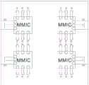
图3为本发明的毫米波信号发射和接收电路层芯片表贴图。FIG. 3 is a map of the chip surface of the millimeter wave signal transmitting and receiving circuit layer of the present invention.
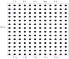
图4为本发明的底部BGA信号输入层结构图。FIG. 4 is a structural diagram of the bottom BGA signal input layer of the present invention.
具体实施方式Detailed ways
本发明采用硅基半导体封装工艺+玻璃基微纳加工工艺,将毫米波微带贴片天线阵列、微波芯片和毫米波芯片三维集成封装。如图1~图4所示,功能电路从上往下依次为:毫米波微带贴片天线阵列层1、天线馈电网络层2、毫米波信号发射和接收电路层3、毫米波信号三维垂直传输层4、毫米波电路屏蔽层5、功分网络和数字信号层6以及底部BGA信号输入层7。毫米波信号及低频信号均从底部BGA信号输入层7馈入。The present invention adopts a silicon-based semiconductor packaging process + a glass-based micro-nano processing process to three-dimensionally integrate the millimeter-wave microstrip patch antenna array, the microwave chip and the millimeter-wave chip. As shown in Figure 1 to Figure 4, the functional circuits from top to bottom are: millimeter wave microstrip patch
毫米波微带贴片天线阵列层1采用低损耗、低介电常数的玻璃作为辐射衬底,天线阵列底部的玻璃为空气腔结构,阵元数目为N×N,制作工艺为基于玻璃的多层布线工艺、激光刻蚀腔体工艺和圆片级键合工艺。The millimeter-wave microstrip patch
天线馈电网络层2中馈线模式为接地共面波导传输线,输入端与毫米波信号发射和接收电路层3的输出口连接,输出端与微带贴片天线连接。The feeder mode in the antenna
毫米波信号三维垂直传输层3内部设置有TSV、Bump和BGA的三维垂直传输结构,一端与相邻的上硅电路板互连,另一端与相邻的下硅电路板互连,实现毫米波信号的垂直传输。The three-dimensional
毫米波信号发射和接收电路层4含有信号发射支路、接收支路和公共支路,MMIC芯片的输入输出接口为Bump形式,不同MMIC芯片的Bump端口通过硅基电路板表面的接地共面波导互连。Millimeter wave signal transmitting and receiving
毫米波电路屏蔽层5采用硅空气腔结构,内部设置有信号TSV和高密度共地TSV。The millimeter-wave
功分网络和数字信号电路层6包括毫米波信号的一分N功分网络、波控电路、给毫米波信号发射和接收电路层4供电的电源调制电路以及无源电路等。The power division network and digital
底部BGA信号输入层7内部设置有细间距的BGA阵列端口,整个AiP阵元的毫米波信号、数字信号以及电源接口从BGA端口馈入。利用TSV实现与功分网络和数字信号电路层6的电气互连。The bottom BGA
进一步的,设计方法采用硅基半导体封装工艺+玻璃基微纳加工工艺。Further, the design method adopts a silicon-based semiconductor packaging process + a glass-based micro-nano processing process.
进一步的,毫米波微带贴片天线阵列层1、毫米波信号发射和接收电路层3和功分网络和数字信号电路层6相互之间利用TSV+Bump+BGA实现三维垂直传输。Further, the millimeter-wave microstrip patch
进一步的,毫米波信号发射和接收电路层3与Bump互连的接地共面波导阻抗为50欧姆。Further, the impedance of the grounded coplanar waveguide interconnecting the millimeter wave signal transmitting and receiving
进一步的,硅基半导体封装工艺,包括TSV工艺、多层布线工艺和深腔刻蚀工艺。硅基TSV深宽比≥10:1,内部用金属铜填实,TSV直径≥20um。硅基电路板正面为三层金属布线+三层介质层工艺,背面为一层金属布线+两层介质层工艺+铜Bump工艺。Further, the silicon-based semiconductor packaging process includes TSV process, multi-layer wiring process and deep cavity etching process. The aspect ratio of silicon-based TSV is ≥10:1, the interior is filled with metal copper, and the diameter of TSV is ≥20um. The front side of the silicon-based circuit board is a three-layer metal wiring + three-layer dielectric layer process, and the back side is a one-layer metal wiring + two-layer dielectric layer process + copper bump process.
进一步的,玻璃基微纳加工工艺,包括TGV工艺、圆片级键合工艺和深腔刻蚀工艺。玻璃基TGV≥20:1,内部用金属填实。Further, glass-based micro-nano processing technology includes TGV technology, wafer-level bonding technology and deep cavity etching technology. Glass-based TGV≥20:1, the interior is filled with metal.
进一步的,三维垂直传输结构TSV、Bump和BGA,频率特性覆盖0-40GHz,回波损耗≤-20dB,插入损耗≤0.5dB/cm。Further, the three-dimensional vertical transmission structures TSV, Bump and BGA have frequency characteristics covering 0-40 GHz, return loss ≤ -20 dB, and insertion loss ≤ 0.5 dB/cm.
进一步的,毫米波信号发射和接收电路层4具有毫米波信号的放大、移相、衰减等功能。Further, the millimeter-wave signal transmitting and receiving
进一步的,毫米波电路屏蔽层5中的硅空气腔结构高度≥400um,内外表面全部溅射金属层,上下互连端口为类同轴结构图形。Further, the height of the silicon air cavity structure in the millimeter-wave
进一步的,功分网络和数字信号电路层6的无源电路集成在硅基电路板中,涵盖电感、电容和电阻。Further, the passive circuits of the power division network and the digital
进一步的,底部BGA信号输入层7采用BGA,直径≤200um,间距≤1000um。Further, the bottom BGA
本发明采用硅基半导体封装工艺和玻璃基微纳加工工艺相结合的三维集成设计方案,可以极大的减小毫米波AiP相控阵阵元的重量和体积,提高性能与能效。The invention adopts a three-dimensional integrated design scheme combining silicon-based semiconductor packaging technology and glass-based micro-nano processing technology, which can greatly reduce the weight and volume of the millimeter-wave AiP phased array element, and improve performance and energy efficiency.
下面结合实施例对本发明进行详细说明。The present invention will be described in detail below with reference to the embodiments.
实施例1Example 1
结合图1,本发明的一种三维集成毫米波AiP相控阵阵元,采用硅基半导体封装工艺和玻璃基微纳加工工艺相结合,将毫米波天线与多层功能电路在Z轴方向上垂直互连。从上往下依次为:毫米波微带贴片天线阵列层1、天线馈电网络层2、毫米波信号发射和接收电路层3、毫米波信号三维垂直传输层4、毫米波电路屏蔽层5、功分网络和数字信号层6以及底部BGA信号输入层7。1, a three-dimensional integrated millimeter-wave AiP phased array element of the present invention adopts the combination of silicon-based semiconductor packaging technology and glass-based micro-nano processing technology, and combines the millimeter-wave antenna and the multi-layer functional circuit in the Z-axis direction. vertical interconnection. From top to bottom: millimeter wave microstrip patch
如图2所示,毫米波微带贴片天线阵元数目为N×N,N≥2,采用低损耗、低介电常数的玻璃作为辐射衬底,玻璃微纳加工工艺包括金属化工艺、激光刻蚀腔体工艺和圆片级键合工艺。其中天线阵列正下方的玻璃为空气腔结构,实现高增益和超宽带。所述空气腔结构为提高天线阵列增益和带宽的关键性结构。As shown in Figure 2, the number of millimeter-wave microstrip patch antenna array elements is N×N, N≥2, and glass with low loss and low dielectric constant is used as the radiation substrate. The glass micro-nano processing technology includes metallization process, Laser etching cavity process and wafer level bonding process. The glass directly under the antenna array is an air cavity structure to achieve high gain and ultra-wideband. The air cavity structure is a key structure for improving the gain and bandwidth of the antenna array.
天线馈线模式为接地共面波导传输线,输入端与毫米波信号发射和接收电路层3的输出口连接,近天线输出端采用耦合馈电方式。The antenna feeder mode is a grounded coplanar waveguide transmission line, the input end is connected to the output port of the millimeter wave signal transmitting and receiving
毫米波信号三维垂直传输通过TSV、Bump和BGA实现,一端与相邻的上硅电路板互连,另一端与相邻的下硅电路板互连,毫米波信号的垂直传输。所述TSV为信号传输的关键行部分。The three-dimensional vertical transmission of millimeter wave signals is realized by TSV, Bump and BGA. One end is interconnected with the adjacent upper silicon circuit board, and the other end is interconnected with the adjacent lower silicon circuit board, and the vertical transmission of millimeter wave signals. The TSV is the critical row portion of the signalling.
如图3所示,毫米波信号发射和接收电路含有信号发射支路、接收支路和公共支路,MMIC芯片的输入输出接口为Bump形式,不同MMIC芯片的Bump端口通过硅基电路板表面的接地共面波导互连。As shown in Figure 3, the millimeter-wave signal transmission and reception circuit includes a signal transmission branch, a receiving branch and a common branch. The input and output interfaces of the MMIC chip are in the form of bumps, and the bump ports of different MMIC chips pass through the surface of the silicon-based circuit board. Ground coplanar waveguide interconnects.
毫米波电路通道间屏蔽方式采用硅空气腔结构,内部设置有信号TSV和高密度共地TSV。The shielding method between the channels of the millimeter-wave circuit adopts a silicon air cavity structure, and there are signal TSVs and high-density common ground TSVs inside.
功分网络和数字信号电路包括毫米波信号的一分N功分网络N≥2、波控电路、给毫米波信号发射和接收电路层4供电的电源调制电路以及无源电路等。The power division network and digital signal circuit include a one-to-N power division network N≥2 for millimeter wave signals, a wave control circuit, a power supply modulation circuit for supplying power to the millimeter wave signal transmitting and receiving
如图4所示,底部BGA信号输入端为细间距的BGA阵列端口,整个AiP阵元的毫米波信号、数字信号以及电源接口从BGA端口馈入。利用TSV实现与功分网络和数字信号电路层6的电气互连。As shown in Figure 4, the bottom BGA signal input terminal is a fine-pitch BGA array port, and the millimeter wave signal, digital signal and power interface of the entire AiP array element are fed from the BGA port. Electrical interconnection with the power division network and digital
实施例2Example 2
如图1所示,一种新型三维集成毫米波AiP相控阵元,其设计架构包括高增益毫米波微带天线阵列、天线馈电网络、毫米波信号发射和接收电路、三维垂直传输电路、不同通道间屏蔽设计、功分网络和数字芯片电路以及细间距BGA端口设计。As shown in Figure 1, a new three-dimensional integrated millimeter-wave AiP phased array element, its design architecture includes a high-gain millimeter-wave microstrip antenna array, an antenna feed network, a millimeter-wave signal transmitting and receiving circuit, a three-dimensional vertical transmission circuit, Shielding design between different channels, power division network and digital chip circuit and fine pitch BGA port design.
如图2所示,毫米波微带贴片天线阵列由2×2=4的玻璃基辐射单元组阵而成,组阵方式为矩形方阵,采用空间耦合的馈电模式。通过激光在玻璃衬底上刻蚀空气腔体,实现2×2矩形天线方阵的高增益、高效率和高带宽。带腔体的玻璃与图形金属化的玻璃通过圆片级键合的方式键合在一起。天线与馈源采用BGA结构互连,有效地减小传统连接器带来的损耗大问题。As shown in Figure 2, the millimeter-wave microstrip patch antenna array is formed by 2×2=4 glass-based radiating elements in an array. The air cavity is etched on the glass substrate by laser, and the high gain, high efficiency and high bandwidth of the 2×2 rectangular antenna array are realized. The glass with cavity and the patterned metallized glass are bonded together by wafer-level bonding. The antenna and the feed are interconnected by the BGA structure, which effectively reduces the large loss caused by the traditional connector.
如图3所示,基于BUMP输入输出接口的MMIC芯片和数字芯片采用表贴的方式安装在高阻硅电路板上,整个相控阵阵元中的各类芯片均采用无金丝引线的互连方式,实现毫米波信号的低插损和数字信号的低延迟。高阻硅电路板内部的TSV深宽比≥10:1,金属铜Cu填实,正面三层布线+三层介质层,背面一层布线+两层介质层+Bump。另外高阻硅电路板表面的毫米波传输线结构为接地共面波导,具有辐射损耗低等特点。四个通道间电磁屏蔽方式采用金属化的高阻硅腔体隔离,腔体内部具有高密度的共地TSV。As shown in Figure 3, the MMIC chip and digital chip based on the BUMP input and output interface are mounted on a high-resistance silicon circuit board in a surface-mount manner. The connection method realizes low insertion loss of millimeter wave signals and low delay of digital signals. The TSV aspect ratio inside the high-resistance silicon circuit board is ≥10:1, the metal copper Cu is filled, the front three layers of wiring + three dielectric layers, the back one layer of wiring + two dielectric layers + bump. In addition, the millimeter-wave transmission line structure on the surface of the high-resistance silicon circuit board is a grounded coplanar waveguide, which has the characteristics of low radiation loss. The electromagnetic shielding method between the four channels is isolated by a metallized high-resistance silicon cavity, and the cavity has a high-density common ground TSV.
2×2毫米波AiP阵元底部采用BGA的表贴封装形式,集成了毫米波信号输入接口、数字逻辑信号输入接口、电源调制输入接口。将多层硅基电路板和玻璃基贴片天线高精度堆叠后(堆叠对准偏差±10um),经过低温回流的方式实现一体化的微型化三维集成毫米波AiP相控阵阵元。The bottom of the 2×2 millimeter-wave AiP array element adopts the BGA surface-mount package, and integrates the millimeter-wave signal input interface, the digital logic signal input interface, and the power modulation input interface. After stacking the multi-layer silicon-based circuit board and the glass-based patch antenna with high precision (the stacking alignment deviation is ±10um), the integrated miniaturized three-dimensional integrated millimeter-wave AiP phased array element is realized by means of low temperature reflow.
Claims (7)
Translated fromChinesePriority Applications (1)
| Application Number | Priority Date | Filing Date | Title |
|---|---|---|---|
| CN201911419918.9ACN111276787B (en) | 2019-12-31 | 2019-12-31 | Three-dimensional integrated millimeter wave AiP phased array element |
Applications Claiming Priority (1)
| Application Number | Priority Date | Filing Date | Title |
|---|---|---|---|
| CN201911419918.9ACN111276787B (en) | 2019-12-31 | 2019-12-31 | Three-dimensional integrated millimeter wave AiP phased array element |
Publications (2)
| Publication Number | Publication Date |
|---|---|
| CN111276787Atrue CN111276787A (en) | 2020-06-12 |
| CN111276787B CN111276787B (en) | 2021-05-07 |
Family
ID=71111848
Family Applications (1)
| Application Number | Title | Priority Date | Filing Date |
|---|---|---|---|
| CN201911419918.9AActiveCN111276787B (en) | 2019-12-31 | 2019-12-31 | Three-dimensional integrated millimeter wave AiP phased array element |
Country Status (1)
| Country | Link |
|---|---|
| CN (1) | CN111276787B (en) |
Cited By (23)
| Publication number | Priority date | Publication date | Assignee | Title |
|---|---|---|---|---|
| CN112051551A (en)* | 2020-09-10 | 2020-12-08 | 上海无线电设备研究所 | Silicon-based three-dimensional integrated micro radar high-frequency high-power active subarray |
| CN112103665A (en)* | 2020-11-09 | 2020-12-18 | 成都天锐星通科技有限公司 | Radio frequency feed network, phased array antenna and communication equipment |
| CN112490222A (en)* | 2020-11-11 | 2021-03-12 | 深圳市信维通信股份有限公司 | Packaging structure of millimeter wave antenna module and mobile device |
| CN112701464A (en)* | 2020-12-28 | 2021-04-23 | 京信网络系统股份有限公司 | Millimeter wave package antenna and array antenna |
| CN112820656A (en)* | 2020-12-31 | 2021-05-18 | 中国科学院空天信息创新研究院 | Three-dimensional integrated packaging method for millimeter wave miniature SAR system |
| CN113013583A (en)* | 2021-01-29 | 2021-06-22 | 中国电子科技集团公司第三十八研究所 | Millimeter wave radar packaging module |
| CN113539998A (en)* | 2021-06-10 | 2021-10-22 | 南京国博电子股份有限公司 | Silicon-based three-dimensional integrated transceiving front end |
| CN113552540A (en)* | 2021-08-24 | 2021-10-26 | 中国科学院上海微系统与信息技术研究所 | Three-dimensional integrated micro-assembly radar front-end module |
| CN113567929A (en)* | 2021-07-12 | 2021-10-29 | 南京国博电子股份有限公司 | 3D heterogeneous integrated multifunctional transceiver chip |
| CN113594716A (en)* | 2021-07-16 | 2021-11-02 | 深圳市信维通信股份有限公司 | LCP plate-based millimeter wave antenna structure and terminal equipment |
| CN113838845A (en)* | 2021-11-26 | 2021-12-24 | 成都雷电微力科技股份有限公司 | TR assembly based on three-dimensional stacked airtight package and assembling method |
| CN114093824A (en)* | 2021-11-05 | 2022-02-25 | 成都雷电微力科技股份有限公司 | Microwave millimeter wave chip airtight packaging structure and method with BGA interface |
| CN114122675A (en)* | 2021-11-15 | 2022-03-01 | 中国电子科技集团公司第三十八研究所 | Expandable millimeter wave phased array unit, preparation method and active antenna array surface |
| CN114614247A (en)* | 2022-03-16 | 2022-06-10 | 南京吉凯微波技术有限公司 | Integrated network of millimeter wave tile-type phased array antenna |
| CN114665280A (en)* | 2022-03-28 | 2022-06-24 | 中国电子科技集团公司第十研究所 | Three-dimensional transmitting-receiving feed network applied to flat-panel packaged array antenna |
| CN115020963A (en)* | 2022-05-06 | 2022-09-06 | 中国科学院微小卫星创新研究院 | Broadband circularly polarized array element suitable for AOP millimeter wave phased array |
| CN115020964A (en)* | 2022-06-14 | 2022-09-06 | 中国电子科技集团公司第十四研究所 | Cascade antenna based on BCB transmission structure |
| CN115173029A (en)* | 2022-05-10 | 2022-10-11 | 中国科学院微小卫星创新研究院 | Wide-beam circularly-polarized microstrip array element suitable for AOP millimeter wave phased array |
| CN115241633A (en)* | 2022-07-12 | 2022-10-25 | 航天科工微系统技术有限公司 | A mmWave packaged antenna based on TGV process |
| CN115425394A (en)* | 2022-08-05 | 2022-12-02 | 中国电子科技集团公司第十四研究所 | Stripline based on laminated structure and laminated array surface antenna unit based on three-dimensional stacking of heterogeneous substrates |
| CN116231290A (en)* | 2022-09-09 | 2023-06-06 | 北京无线电测量研究所 | Three-dimensional stacked phased array antenna |
| CN116545479A (en)* | 2023-04-12 | 2023-08-04 | 中国电子科技集团公司第三十八研究所 | A large-scale ultra-dense multi-beam antenna system |
| CN117039369A (en)* | 2023-08-16 | 2023-11-10 | 中国电子科技集团公司第十四研究所 | Three-dimensional stacked glass TGV substrate switch filter bank |
Citations (11)
| Publication number | Priority date | Publication date | Assignee | Title |
|---|---|---|---|---|
| JP2009038696A (en)* | 2007-08-03 | 2009-02-19 | Toyota Central R&D Labs Inc | Integrated circuit package with antenna |
| WO2009118694A1 (en)* | 2008-03-25 | 2009-10-01 | Nxp B.V. | Integrated 3d high density and high quality inductive element |
| CN102405524A (en)* | 2009-02-20 | 2012-04-04 | 国家半导体公司 | Integrated circuit micro-module |
| US9153863B2 (en)* | 2012-01-24 | 2015-10-06 | E I Du Pont De Nemours And Company | Low temperature co-fired ceramic (LTCC) system in a package (SiP) configurations for microwave/millimeter wave packaging applications |
| US20150340765A1 (en)* | 2014-05-20 | 2015-11-26 | International Business Machines Corporation | Integration of area efficient antennas for phased array or wafer scale array antenna applications |
| CN106575823A (en)* | 2014-05-02 | 2017-04-19 | 希尔莱特有限责任公司 | Surface scattering antennas with lumped elements |
| CN107275226A (en)* | 2017-07-02 | 2017-10-20 | 中国航空工业集团公司雷华电子技术研究所 | A kind of radio frequency component integrated approach |
| CN107910320A (en)* | 2017-12-07 | 2018-04-13 | 中芯长电半导体(江阴)有限公司 | Semiconductor structure with antenna module and preparation method thereof |
| CN108172564A (en)* | 2017-12-24 | 2018-06-15 | 中国电子科技集团公司第五十五研究所 | A three-dimensional integrated package of millimeter wave antenna and silicon-based components |
| US10115671B2 (en)* | 2012-08-03 | 2018-10-30 | Snaptrack, Inc. | Incorporation of passives and fine pitch through via for package on package |
| EP3512034A1 (en)* | 2018-01-12 | 2019-07-17 | INTEL Corporation | On-package integrated stiffener antenna |
- 2019
- 2019-12-31CNCN201911419918.9Apatent/CN111276787B/enactiveActive
Patent Citations (11)
| Publication number | Priority date | Publication date | Assignee | Title |
|---|---|---|---|---|
| JP2009038696A (en)* | 2007-08-03 | 2009-02-19 | Toyota Central R&D Labs Inc | Integrated circuit package with antenna |
| WO2009118694A1 (en)* | 2008-03-25 | 2009-10-01 | Nxp B.V. | Integrated 3d high density and high quality inductive element |
| CN102405524A (en)* | 2009-02-20 | 2012-04-04 | 国家半导体公司 | Integrated circuit micro-module |
| US9153863B2 (en)* | 2012-01-24 | 2015-10-06 | E I Du Pont De Nemours And Company | Low temperature co-fired ceramic (LTCC) system in a package (SiP) configurations for microwave/millimeter wave packaging applications |
| US10115671B2 (en)* | 2012-08-03 | 2018-10-30 | Snaptrack, Inc. | Incorporation of passives and fine pitch through via for package on package |
| CN106575823A (en)* | 2014-05-02 | 2017-04-19 | 希尔莱特有限责任公司 | Surface scattering antennas with lumped elements |
| US20150340765A1 (en)* | 2014-05-20 | 2015-11-26 | International Business Machines Corporation | Integration of area efficient antennas for phased array or wafer scale array antenna applications |
| CN107275226A (en)* | 2017-07-02 | 2017-10-20 | 中国航空工业集团公司雷华电子技术研究所 | A kind of radio frequency component integrated approach |
| CN107910320A (en)* | 2017-12-07 | 2018-04-13 | 中芯长电半导体(江阴)有限公司 | Semiconductor structure with antenna module and preparation method thereof |
| CN108172564A (en)* | 2017-12-24 | 2018-06-15 | 中国电子科技集团公司第五十五研究所 | A three-dimensional integrated package of millimeter wave antenna and silicon-based components |
| EP3512034A1 (en)* | 2018-01-12 | 2019-07-17 | INTEL Corporation | On-package integrated stiffener antenna |
Cited By (33)
| Publication number | Priority date | Publication date | Assignee | Title |
|---|---|---|---|---|
| CN112051551B (en)* | 2020-09-10 | 2024-01-02 | 上海无线电设备研究所 | Silicon-based three-dimensional integrated micro radar high-frequency high-power active sub-array |
| CN112051551A (en)* | 2020-09-10 | 2020-12-08 | 上海无线电设备研究所 | Silicon-based three-dimensional integrated micro radar high-frequency high-power active subarray |
| CN112103665A (en)* | 2020-11-09 | 2020-12-18 | 成都天锐星通科技有限公司 | Radio frequency feed network, phased array antenna and communication equipment |
| CN112490222A (en)* | 2020-11-11 | 2021-03-12 | 深圳市信维通信股份有限公司 | Packaging structure of millimeter wave antenna module and mobile device |
| CN112701464A (en)* | 2020-12-28 | 2021-04-23 | 京信网络系统股份有限公司 | Millimeter wave package antenna and array antenna |
| CN112701464B (en)* | 2020-12-28 | 2024-04-26 | 京信网络系统股份有限公司 | Millimeter wave packaged antennas and array antennas |
| CN112820656A (en)* | 2020-12-31 | 2021-05-18 | 中国科学院空天信息创新研究院 | Three-dimensional integrated packaging method for millimeter wave miniature SAR system |
| CN113013583A (en)* | 2021-01-29 | 2021-06-22 | 中国电子科技集团公司第三十八研究所 | Millimeter wave radar packaging module |
| CN113013583B (en)* | 2021-01-29 | 2023-08-18 | 中国电子科技集团公司第三十八研究所 | Millimeter wave radar packaging module |
| CN113539998A (en)* | 2021-06-10 | 2021-10-22 | 南京国博电子股份有限公司 | Silicon-based three-dimensional integrated transceiving front end |
| CN113539998B (en)* | 2021-06-10 | 2024-06-04 | 南京国博电子股份有限公司 | Silicon-based three-dimensional integrated transceiver front end |
| CN113567929A (en)* | 2021-07-12 | 2021-10-29 | 南京国博电子股份有限公司 | 3D heterogeneous integrated multifunctional transceiver chip |
| CN113567929B (en)* | 2021-07-12 | 2024-08-06 | 南京国博电子股份有限公司 | 3D heterogeneous integrated multifunctional transceiver chip |
| CN113594716A (en)* | 2021-07-16 | 2021-11-02 | 深圳市信维通信股份有限公司 | LCP plate-based millimeter wave antenna structure and terminal equipment |
| CN113552540A (en)* | 2021-08-24 | 2021-10-26 | 中国科学院上海微系统与信息技术研究所 | Three-dimensional integrated micro-assembly radar front-end module |
| CN114093824A (en)* | 2021-11-05 | 2022-02-25 | 成都雷电微力科技股份有限公司 | Microwave millimeter wave chip airtight packaging structure and method with BGA interface |
| CN114122675A (en)* | 2021-11-15 | 2022-03-01 | 中国电子科技集团公司第三十八研究所 | Expandable millimeter wave phased array unit, preparation method and active antenna array surface |
| CN114122675B (en)* | 2021-11-15 | 2024-06-04 | 中国电子科技集团公司第三十八研究所 | Expandable millimeter wave phased array unit, preparation method and active antenna array surface |
| CN113838845A (en)* | 2021-11-26 | 2021-12-24 | 成都雷电微力科技股份有限公司 | TR assembly based on three-dimensional stacked airtight package and assembling method |
| CN113838845B (en)* | 2021-11-26 | 2022-02-11 | 成都雷电微力科技股份有限公司 | TR assembly based on three-dimensional stacked airtight package and assembling method |
| CN114614247A (en)* | 2022-03-16 | 2022-06-10 | 南京吉凯微波技术有限公司 | Integrated network of millimeter wave tile-type phased array antenna |
| CN114665280A (en)* | 2022-03-28 | 2022-06-24 | 中国电子科技集团公司第十研究所 | Three-dimensional transmitting-receiving feed network applied to flat-panel packaged array antenna |
| CN115020963A (en)* | 2022-05-06 | 2022-09-06 | 中国科学院微小卫星创新研究院 | Broadband circularly polarized array element suitable for AOP millimeter wave phased array |
| CN115173029A (en)* | 2022-05-10 | 2022-10-11 | 中国科学院微小卫星创新研究院 | Wide-beam circularly-polarized microstrip array element suitable for AOP millimeter wave phased array |
| CN115020964B (en)* | 2022-06-14 | 2024-04-23 | 中国电子科技集团公司第十四研究所 | Laminated antenna based on BCB transmission structure |
| CN115020964A (en)* | 2022-06-14 | 2022-09-06 | 中国电子科技集团公司第十四研究所 | Cascade antenna based on BCB transmission structure |
| CN115241633A (en)* | 2022-07-12 | 2022-10-25 | 航天科工微系统技术有限公司 | A mmWave packaged antenna based on TGV process |
| CN115425394B (en)* | 2022-08-05 | 2024-02-27 | 中国电子科技集团公司第十四研究所 | Strip line based on laminated structure and laminated array antenna unit based on heterogeneous substrate three-dimensional stacking |
| CN115425394A (en)* | 2022-08-05 | 2022-12-02 | 中国电子科技集团公司第十四研究所 | Stripline based on laminated structure and laminated array surface antenna unit based on three-dimensional stacking of heterogeneous substrates |
| CN116231290A (en)* | 2022-09-09 | 2023-06-06 | 北京无线电测量研究所 | Three-dimensional stacked phased array antenna |
| CN116545479A (en)* | 2023-04-12 | 2023-08-04 | 中国电子科技集团公司第三十八研究所 | A large-scale ultra-dense multi-beam antenna system |
| CN117039369A (en)* | 2023-08-16 | 2023-11-10 | 中国电子科技集团公司第十四研究所 | Three-dimensional stacked glass TGV substrate switch filter bank |
| CN117039369B (en)* | 2023-08-16 | 2024-04-23 | 中国电子科技集团公司第十四研究所 | Three-dimensional stacked glass TGV substrate switch filter bank |
Also Published As
| Publication number | Publication date |
|---|---|
| CN111276787B (en) | 2021-05-07 |
Similar Documents
| Publication | Publication Date | Title |
|---|---|---|
| CN111276787B (en) | Three-dimensional integrated millimeter wave AiP phased array element | |
| US9196951B2 (en) | Millimeter-wave radio frequency integrated circuit packages with integrated antennas | |
| CN108172564B (en) | Three-dimensional integrated package of millimeter wave antenna and silicon-based component | |
| CN108649019B (en) | Fan-Out Package Structure | |
| US7808434B2 (en) | Systems and methods for integrated antennae structures in multilayer organic-based printed circuit devices | |
| US8648454B2 (en) | Wafer-scale package structures with integrated antennas | |
| US9153863B2 (en) | Low temperature co-fired ceramic (LTCC) system in a package (SiP) configurations for microwave/millimeter wave packaging applications | |
| EP2253045B1 (en) | Radio frequency (rf) integrated circuit (ic) packages with integrated aperture-coupled patch antenna(s) | |
| US7675465B2 (en) | Surface mountable integrated circuit packaging scheme | |
| CN104332413A (en) | 3D assembling method for integrally integrating chips of T/R assembly | |
| Heyen et al. | Novel LTCC/BGA modules for highly integrated millimeter-wave transceivers | |
| EP2178119B1 (en) | Surface mountable integrated circuit package | |
| CN113140887B (en) | Packaged antenna and method of manufacturing the same | |
| KR20150108147A (en) | Radar on a package for millimeter wave and radar assembly using the same | |
| Govindarajulu et al. | A 60 GHz millimeter-wave antenna array for 3D antenna-in-package applications | |
| CN113539998B (en) | Silicon-based three-dimensional integrated transceiver front end | |
| CN114496996B (en) | Electromagnetic shielding structure of a TR component | |
| CN117673037B (en) | Millimeter wave chip transmission structure | |
| CN116895614A (en) | Millimeter wave system packaging structure integrated by three-dimensional isomerism | |
| CN115693101B (en) | W-band transmit-receive integrated phased array packaged antenna and manufacturing process | |
| CN115332779B (en) | Packaging components for phased array antennas | |
| CN115241633B (en) | A millimeter wave packaged antenna based on TGV technology | |
| CN115172307A (en) | High-thermal-conductivity silicon-based composite interconnection network | |
| CN220527176U (en) | W frequency band transmission line-waveguide vertical transmission conversion structure | |
| Xia et al. | Design of Miniaturized Silicon Based SiP TR Module |
Legal Events
| Date | Code | Title | Description |
|---|---|---|---|
| PB01 | Publication | ||
| PB01 | Publication | ||
| SE01 | Entry into force of request for substantive examination | ||
| SE01 | Entry into force of request for substantive examination | ||
| GR01 | Patent grant | ||
| GR01 | Patent grant | ||
| TR01 | Transfer of patent right | ||
| TR01 | Transfer of patent right | Effective date of registration:20211201 Address after:210000 room 4001, Dongfang Building, No. 1, Dongji Avenue, Jiangning District, Nanjing, Jiangsu Province (Jiangning Development Zone) Patentee after:Nanjing guomicroelectronics Co., Ltd Address before:210016 No. 524 East Zhongshan Road, Jiangsu, Nanjing Patentee before:CHINA ELECTRONICS TECHNOLOGY GROUP CORPORATION NO.55 Research Institute |