CN111276505A - Miniature light-emitting diode display device and manufacturing method thereof - Google Patents
Miniature light-emitting diode display device and manufacturing method thereofDownload PDFInfo
- Publication number
- CN111276505A CN111276505ACN201811481569.9ACN201811481569ACN111276505ACN 111276505 ACN111276505 ACN 111276505ACN 201811481569 ACN201811481569 ACN 201811481569ACN 111276505 ACN111276505 ACN 111276505A
- Authority
- CN
- China
- Prior art keywords
- area
- light emitting
- micro light
- display substrate
- micro
- Prior art date
- Legal status (The legal status is an assumption and is not a legal conclusion. Google has not performed a legal analysis and makes no representation as to the accuracy of the status listed.)
- Granted
Links
- 238000004519manufacturing processMethods0.000titleclaimsabstractdescription13
- 239000000758substrateSubstances0.000claimsabstractdescription132
- 238000012546transferMethods0.000claimsdescription177
- 238000000034methodMethods0.000claimsdescription29
- 230000003247decreasing effectEffects0.000claims1
- 230000008569processEffects0.000description14
- 238000013461designMethods0.000description7
- 238000009826distributionMethods0.000description7
- 230000000694effectsEffects0.000description5
- 238000012545processingMethods0.000description5
- 230000008859changeEffects0.000description2
- 230000007423decreaseEffects0.000description2
- 238000011161developmentMethods0.000description2
- 238000005516engineering processMethods0.000description2
- 230000004044responseEffects0.000description2
- 238000001179sorption measurementMethods0.000description2
- 238000003860storageMethods0.000description2
- 230000009471actionEffects0.000description1
- 239000000853adhesiveSubstances0.000description1
- 230000001070adhesive effectEffects0.000description1
- 238000004458analytical methodMethods0.000description1
- 238000004364calculation methodMethods0.000description1
- 235000019800disodium phosphateNutrition0.000description1
- 239000011159matrix materialSubstances0.000description1
- 238000012986modificationMethods0.000description1
- 230000004048modificationEffects0.000description1
- 230000005693optoelectronicsEffects0.000description1
- 238000011160researchMethods0.000description1
- 229910052594sapphireInorganic materials0.000description1
- 239000010980sapphireSubstances0.000description1
- 239000004065semiconductorSubstances0.000description1
- 230000007704transitionEffects0.000description1
- 238000013519translationMethods0.000description1
Images


Classifications
- H—ELECTRICITY
- H10—SEMICONDUCTOR DEVICES; ELECTRIC SOLID-STATE DEVICES NOT OTHERWISE PROVIDED FOR
- H10H—INORGANIC LIGHT-EMITTING SEMICONDUCTOR DEVICES HAVING POTENTIAL BARRIERS
- H10H29/00—Integrated devices, or assemblies of multiple devices, comprising at least one light-emitting semiconductor element covered by group H10H20/00
- H10H29/10—Integrated devices comprising at least one light-emitting semiconductor component covered by group H10H20/00
- H10H29/14—Integrated devices comprising at least one light-emitting semiconductor component covered by group H10H20/00 comprising multiple light-emitting semiconductor components
- H10H29/142—Two-dimensional arrangements, e.g. asymmetric LED layout
- H—ELECTRICITY
- H10—SEMICONDUCTOR DEVICES; ELECTRIC SOLID-STATE DEVICES NOT OTHERWISE PROVIDED FOR
- H10H—INORGANIC LIGHT-EMITTING SEMICONDUCTOR DEVICES HAVING POTENTIAL BARRIERS
- H10H20/00—Individual inorganic light-emitting semiconductor devices having potential barriers, e.g. light-emitting diodes [LED]
- H10H20/80—Constructional details
- H10H20/85—Packages
- H10H20/857—Interconnections, e.g. lead-frames, bond wires or solder balls
Landscapes
- Devices For Indicating Variable Information By Combining Individual Elements (AREA)
- Led Device Packages (AREA)
Abstract
Translated fromChinese
Description
Translated fromChinese技术领域technical field
本发明涉及一种显示装置,尤其涉及一种微型发光二极管显示装置及其制作方法。The present invention relates to a display device, in particular to a miniature light-emitting diode display device and a manufacturing method thereof.
背景技术Background technique
随着显示技术的发展,因微型发光二极管能够满足薄化、微小化以及阵列化的需求,并且具备发光效率高、亮度高、对比值高、可靠度佳以及反应时间快等优势,相关厂商无不看好此新一代显示技术的前景而积极投入开发与研究。With the development of display technology, because miniature light-emitting diodes can meet the needs of thinning, miniaturization and arraying, and have the advantages of high luminous efficiency, high brightness, high contrast value, good reliability and fast response time, relevant manufacturers are all Optimistic about the prospects of this new generation of display technology and actively invest in development and research.
在将成型于成长基板上的微型发光二极管转移至显示基板的过程中,所需的微型发光二极管为数十万或数百万颗,大多采分批转移的方式来完成。常见的转移方式例如是:通过磁吸附力或静电吸附力抓取成长基板上的微型发光二极管,并转移至显示基板。每一次转移程序中,转移元件所抓取的微型发光二极管的数量固定且呈矩阵排列。因此,转移至显示基板上后的微型发光二极管可被概分为数个矩形区块,基于每一次转移程序中所可能产生的制程误差或抓取范围的光电特性差异,可能导致相邻的任两矩形区块内的微型发光二极管的光场分布产生差异。据此,在显示基板运作时,观看者可能会察觉到相邻的任两矩形区块之间存在明显的边界,因而存在的显示品质不佳的问题。In the process of transferring the micro light emitting diodes formed on the growth substrate to the display substrate, hundreds of thousands or millions of micro light emitting diodes are required, and most of the micro light emitting diodes are transferred in batches. A common transfer method is, for example, grasping the miniature light-emitting diodes on the growth substrate by magnetic adsorption force or electrostatic adsorption force, and transferring them to the display substrate. In each transfer procedure, the number of micro-LEDs captured by the transfer element is fixed and arranged in a matrix. Therefore, the micro light-emitting diodes transferred to the display substrate can be roughly divided into several rectangular blocks. Based on the process error or the difference in the optoelectronic characteristics of the grasping range that may occur in each transfer process, any two adjacent ones may be caused. The light field distribution of the miniature light-emitting diodes in the rectangular block is different. Accordingly, during the operation of the display substrate, the viewer may perceive that there is a clear boundary between any two adjacent rectangular blocks, thus resulting in a problem of poor display quality.
发明内容SUMMARY OF THE INVENTION
本发明提供一种微型发光二极管显示装置及其制作方法,其具有良好的显示品质。The present invention provides a miniature light emitting diode display device and a manufacturing method thereof, which have good display quality.
本发明的微型发光二极管显示装置包括显示基板、多个导电接垫对以及多个微型发光元件。显示基板具有第一设置区、连接第一设置区的拼接区以及连接拼接区的第二设置区。其中拼接区位于第一设置区与第二设置区之间。其中拼接区具有多个第一填补位置与多个第二填补位置。在排列方向上这些第一填补位置与这些第二填补位置交错设置。多个导电接垫对,以相同的间距阵列设置于显示基板的第一设置区、拼接区与第二设置区。其中在拼接区中各第一填补位置、各第二填补位置分别具有至少一个导电接垫对。多个微型发光元件,设置于显示基板,并分别电性接合至这些导电接垫对。其中,在拼接区中,设置于第一填补位置与第二填补位置中的微型发光元件相对于所接合的导电接垫对具有不同的偏移量。The micro light emitting diode display device of the present invention includes a display substrate, a plurality of conductive pad pairs and a plurality of micro light emitting elements. The display substrate has a first setting area, a splicing area connected with the first setting area, and a second setting area connected with the splicing area. The splicing area is located between the first setting area and the second setting area. The splicing area has a plurality of first filling positions and a plurality of second filling positions. The first padding positions and the second padding positions are alternately arranged in the arrangement direction. A plurality of conductive pad pairs are arranged in the first setting area, the splicing area and the second setting area of the display substrate in an array with the same pitch. Wherein, each first filling position and each second filling position in the splicing area respectively have at least one conductive pad pair. A plurality of micro light-emitting elements are disposed on the display substrate, and are respectively electrically connected to the pairs of conductive pads. Wherein, in the splicing area, the micro light-emitting elements disposed in the first filling position and the second filling position have different offsets with respect to the connected conductive pad pair.
在本发明的一实施例中,设置于第一填补位置与第一设置区中的这些微型发光元件相对于所接合的这些导电接垫对具有相同的偏移量,设置于第二填补位置与第二设置区中的这些微型发光元件相对于所接合的这些导电接垫对具有相同的偏移量。In an embodiment of the present invention, the micro light-emitting elements disposed at the first filling position and the first setting area have the same offset relative to the conductive pad pairs to be bonded, and the micro light-emitting elements disposed at the second filling position and The micro-light emitting elements in the second setting area have the same offset with respect to the bonded pairs of conductive pads.
在本发明的一实施例中,在另一排列方向上这些第一填补位置与这些第二填补位置交错设置。In an embodiment of the present invention, the first padding positions and the second padding positions are arranged alternately in another arrangement direction.
在本发明的一实施例中,上述的各导电接垫对具有分隔的N型接垫与P型接垫以及垂直于显示基板的基准线,且基准线通过N型接垫与P型接垫之间的中点。In an embodiment of the present invention, each of the above-mentioned conductive pad pairs has separate N-type pads and P-type pads and a reference line perpendicular to the display substrate, and the reference line passes through the N-type pad and the P-type pad midpoint between.
在本发明的一实施例中,上述的各微型发光元件的侧壁与对应的导电接垫对的基准线相距一距离,此距离为偏移量。In an embodiment of the present invention, the sidewalls of the above-mentioned micro light-emitting elements are separated from the reference line of the corresponding pair of conductive pads by a distance, and the distance is an offset.
在本发明的一实施例中,上述的这些微型发光元件的边长小于100um。In an embodiment of the present invention, the side lengths of the above-mentioned micro light-emitting elements are less than 100um.
在本发明的一实施例中,在拼接区且沿排列方向上的任两相邻第一填补位置中的两微型发光元件间距不同于任两相邻的第一填补位置、第二填补位置中的两微型发光元件间距。In an embodiment of the present invention, the distance between two micro-light-emitting elements in any two adjacent first filling positions along the arrangement direction in the splicing area is different from any two adjacent first filling positions and second filling positions The distance between the two micro light-emitting elements.
在本发明的一实施例中,分别在第一设置区与拼接区的第一填补位置的两相邻微型发光元件间距不同于分别在第一设置区与拼接区的第二填补位置的两相邻微型发光元件间距。In an embodiment of the present invention, the distance between two adjacent micro-light-emitting elements at the first filling positions of the first setting area and the splicing area is different from the two-phase distance between the second filling positions of the first setting area and the splicing area, respectively. The distance between adjacent micro light-emitting elements.
在本发明的一实施例中,在上述的在显示基板的排列方向上,相近的二个第二填补位置由至少一个第一填补位置分隔开来,相近的二个第一填补位置由至少一个第二填补位置分隔开来。In an embodiment of the present invention, in the above-mentioned arrangement direction of the display substrate, two adjacent second filling positions are separated by at least one first filling position, and two adjacent first filling positions are separated by at least one first filling position. A second padding position is separated.
在本发明的一实施例中,上述的这些第一填补位置在显示基板的排列方向上的数量等于这些第二填补位置在显示基板的排列方向上的数量,且是采随机分布。In an embodiment of the present invention, the number of the above-mentioned first padding positions in the arrangement direction of the display substrate is equal to the number of the second padding positions in the arrangement direction of the display substrate, and is randomly distributed.
在本发明的一实施例中,上述这些第一填补位置依据拼接区的中线呈对称分布。In an embodiment of the present invention, the above-mentioned first filling positions are symmetrically distributed according to the center line of the splicing area.
在本发明的一实施例中,上述的拼接区采多行分布,其中拼接区的每一行中的这些第一填补位置的数量朝远离第一设置区的方向递减。In an embodiment of the present invention, the above-mentioned splicing area is distributed in multiple rows, wherein the number of the first filling positions in each row of the splicing area decreases in the direction away from the first setting area.
本发明的微型发光二极管显示装置包括显示基板、多个导电接垫对以及多个微型发光元件。显示基板具有第一设置区、连接第一设置区的拼接区以及连接拼接区的第二设置区。其中拼接区位于第一设置区与第二设置区之间,其中拼接区具有多个第一填补位置与多个第二填补位置,在排列方向上这些第一填补位置与这些第二填补位置交错设置。多个导电接垫对设置于显示基板上且成群地阵列分布于第一设置区、拼接区与第二设置区中。其中在拼接区的各第一填补位置、各第二填补位置分别具有三个导电接垫对。多个微型发光元件设置于显示基板上并分别电性接合至这些导电接垫对。其中这些多个微型发光元件包括多个第一光色发光二极管、多个第二光色发光二极管与多个第三光色发光二极管,各第一填补位置、各第二填补位置分别设置一个第一光色发光二极管、一个第二光色发光二极管与一个第三光色发光二极管于三个导电接垫对,设置于第一填补位置与第二填补位置中的这些第一色光发光二极管相对于所接合的导电接垫对具有不同的偏移量。The micro light emitting diode display device of the present invention includes a display substrate, a plurality of conductive pad pairs and a plurality of micro light emitting elements. The display substrate has a first setting area, a splicing area connected with the first setting area, and a second setting area connected with the splicing area. The splicing area is located between the first setting area and the second setting area, wherein the splicing area has a plurality of first filling positions and a plurality of second filling positions, and the first filling positions and the second filling positions are staggered in the arrangement direction set up. A plurality of conductive pad pairs are arranged on the display substrate and are distributed in groups in the first arrangement area, the splicing area and the second arrangement area. There are three pairs of conductive pads at each first filling position and each second filling position in the splicing area. A plurality of micro light-emitting elements are disposed on the display substrate and are respectively electrically connected to the pairs of conductive pads. The plurality of micro light-emitting elements include a plurality of light-emitting diodes of a first light color, a plurality of light-emitting diodes of a second light color, and a plurality of light-emitting diodes of a third light color, and each first filling position and each second filling position are respectively provided with a first A light-color LED, a second light-color LED, and a third light-color LED are located on three pairs of conductive pads, and the first fill-in position and the second fill-in position are opposite to the first-color light-emitting diodes The conductive pad pairs to be joined have different offsets.
在本发明的一实施例中,设置于第一填补位置与第一设置区中的这些第一光色发光二极管相对于所接合的这些导电接垫对具有相同的偏移量,设置于第二填补位置与第二设置区中的这些第一光色发光二极管相对于所接合的这些导电接垫对具有相同的偏移量。In an embodiment of the present invention, the first light-color LEDs disposed in the first filling position and the first disposing area have the same offset with respect to the connected conductive pad pairs, and are disposed in the second The filling positions and the first light-color LEDs in the second setting area have the same offset relative to the bonded conductive pad pairs.
在本发明的一实施例中,在拼接区且沿排列方向上的其中一第一填补位置中的第一光色发光二极管与相邻的另一第一填补位置中的第一光色发光二极管之间的间距不同于其中一第一填补位置中的第一光色发光二极管与相邻的另一第二填补位置中的第一光色发光二极管之间的间距。In an embodiment of the present invention, the first light-color LED in one of the first filling positions and the first light-color LED in another adjacent first filling position in the splicing area and along the arrangement direction The distance therebetween is different from the distance between the first light-color LED in one of the first filling positions and the first light-color LED in another adjacent second filling position.
在本发明的一实施例中,分别在第一设置区与拼接区的第一填补位置的两相邻第一光色发光二极管间距不同于分别在第一设置区与拼接区的第二填补位置的两相邻第一光色发光二极管间距。In an embodiment of the present invention, the spacing between two adjacent first light-color LEDs at the first filling positions in the first setting area and the splicing area is different from the second filling positions in the first setting area and the splicing area, respectively. The distance between two adjacent first light color LEDs.
本发明的微型发光二极管显示装置的制作方法包括以下步骤。首先,提供显示基板,其包括阵列设置的多个导电接垫对。接着,提供载板,其设有多个微型发光元件。然后,提供转移元件。之后,通过转移元件将这些微型发光元件分次由载板转移至显示基板,并使这些微型发光元件电性接合至这些导电接垫对。进一步来说,在第n次转移时,转移元件对准载板的一个区域,并且,在转移元件产生第一图案转移区,以通过第一图案转移区将此区域内的这些微型发光元件的第一部分转移至显示基板,并使这些微型发光元件的第二部分留置于此区域内,且在显示基板对应此区域范围中定义出多个空缺位置。在第n+1次转移时,转移元件对准载板的另一区域,转移元件产生第二图案转移区,以通过第二图案转移区将多个微型发光元件转移至显示基板并填补在第n次转移时定义的这些空缺位置。其中,n为正整数,且大于等于1。The manufacturing method of the miniature light emitting diode display device of the present invention includes the following steps. First, a display substrate is provided, which includes a plurality of pairs of conductive pads arranged in an array. Next, a carrier is provided, which is provided with a plurality of micro light-emitting elements. Then, the transfer element is provided. After that, the micro light-emitting elements are transferred from the carrier board to the display substrate in stages by the transfer element, and the micro light-emitting elements are electrically bonded to the conductive pad pairs. Further, during the n-th transfer, the transfer element is aligned with an area of the carrier, and a first pattern transfer area is generated in the transfer element, so that the micro-light-emitting elements in this area can be moved by the first pattern transfer area. The first part is transferred to the display substrate, and the second part of the micro light-emitting elements is left in this area, and a plurality of vacant positions are defined in the range of the display substrate corresponding to this area. During the n+1th transfer, the transfer element is aligned with another area of the carrier, and the transfer element generates a second pattern transfer area, so as to transfer a plurality of micro light-emitting elements to the display substrate through the second pattern transfer area and fill in the second pattern transfer area. These vacancies are defined at n transitions. Among them, n is a positive integer and is greater than or equal to 1.
在本发明的一实施例中,上述的各导电接垫对具有垂直于显示基板的基准线。第n次转移至显示基板的各微型发光元件的侧壁与对应的导电接垫对的基准线相距第一距离,且第n+1次转移至显示基板的各微型发光元件的侧壁与对应的导电接垫对的基准线相距第二距离。第二距离不同于第一距离。In an embodiment of the present invention, each of the above-mentioned pairs of conductive pads has a reference line perpendicular to the display substrate. The sidewall of each micro-light-emitting element transferred to the display substrate for the nth time is separated from the reference line of the corresponding conductive pad pair by a first distance, and the sidewall of each micro-light-emitting element transferred to the display substrate for the n+1th time is the same as the reference line of the corresponding conductive pad pair. The reference lines of the conductive pad pairs are separated by a second distance. The second distance is different from the first distance.
在本发明的一实施例中,上述的第一图案转移区与第二图案转移区的局部轮廓相契合。在使第二图案转移区的图像相对于第一图案转移区的图像偏移或旋转后,第二图案转移区的图像拼接于第一图案转移区的图像。In an embodiment of the present invention, the above-mentioned first pattern transfer area and the partial outline of the second pattern transfer area are consistent with each other. After shifting or rotating the image of the second pattern transfer area relative to the image of the first pattern transfer area, the image of the second pattern transfer area is stitched to the image of the first pattern transfer area.
基于上述,本发明的微型发光二极管显示装置的制作方法是使转移元件产生的局部区域产生转移力而转移特定数量与分布方式的微型发光元件,且转移程序在先的微型发光元件的周围留有空缺位置以供且转移程序在后的微型发光元件填补。基于此,显示基板上的相邻的任两设置区之间的拼接区内存在两不同偏移量的微型发光元件,在微型发光二极管显示装置运作时,此拼接区可提供模糊化的效果,使得的相邻的任两设置区相拼接处不会产生明显边界,以提升微型发光二极管显示装置的显示品质。Based on the above, the manufacturing method of the micro light emitting diode display device of the present invention is to make the local area generated by the transfer element generate a transfer force to transfer a specific number and distribution of micro light emitting elements, and the micro light emitting element before the transfer process is left around. The vacant position is filled by the micro light-emitting element after the transfer procedure. Based on this, there are two micro-light-emitting elements with different offsets in the splicing area between any two adjacent setting areas on the display substrate. When the micro-LED display device operates, the splicing area can provide a blurring effect. There is no obvious boundary at the splicing of any two adjacent setting areas, so as to improve the display quality of the micro light emitting diode display device.
为让本发明的上述特征和优点能更明显易懂,下文特举实施例,并配合附图作详细说明如下。In order to make the above-mentioned features and advantages of the present invention more obvious and easy to understand, the following embodiments are given and described in detail with the accompanying drawings as follows.
附图说明Description of drawings
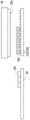
图1A是本发明第一实施例的显示基板的局部俯视示意图。FIG. 1A is a partial top plan view of the display substrate according to the first embodiment of the present invention.
图1B是图1A沿剖线A-A’的局部剖面示意图。Fig. 1B is a schematic partial cross-sectional view of Fig. 1A along section line A-A'.
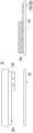
图2A至图2D是图1A的微型发光二极管显示装置的制作流程的侧视示意图。2A to 2D are schematic side views of a manufacturing process of the micro LED display device of FIG. 1A .
图3A是图2A的载板与显示基板的局部俯视示意图,且示出载板上的微型发光元件尚未被抓取时的状态。FIG. 3A is a partial top plan view of the carrier board and the display substrate of FIG. 2A , and shows a state when the micro light-emitting elements on the carrier board have not been grasped.
图3B是图2A的转移元件的转移面的示意图。Figure 3B is a schematic illustration of the transfer face of the transfer element of Figure 2A.
图3C是图2B的显示基板的局部俯视示意图。FIG. 3C is a partial top schematic view of the display substrate of FIG. 2B .
图3D是图2C的载板的局部俯视示意图。FIG. 3D is a partial top schematic view of the carrier plate of FIG. 2C .
图3E是图2C的转移元件的转移面的示意图。Figure 3E is a schematic illustration of the transfer face of the transfer element of Figure 2C.
图4是本发明第二实施例的显示基板的局部俯视示意图。FIG. 4 is a partial top plan view of the display substrate according to the second embodiment of the present invention.
图5是本发明第三实施例的显示基板的局部俯视示意图。FIG. 5 is a partial top plan view of a display substrate according to a third embodiment of the present invention.
图6是本发明第四实施例的显示基板的局部俯视示意图。FIG. 6 is a partial top plan view of a display substrate according to a fourth embodiment of the present invention.
图7是本发明第五实施例的显示基板的局部俯视示意图。FIG. 7 is a partial top plan view of a display substrate according to a fifth embodiment of the present invention.
图8是本发明第六实施例的显示基板的局部俯视示意图。FIG. 8 is a partial top plan view of a display substrate according to a sixth embodiment of the present invention.
附图标记说明:Description of reference numbers:
20:转移元件;20: transfer element;
20a:转移面;20a: transfer surface;
21:第一图案转移区;21: the first pattern transfer area;
22:第二图案转移区;22: the second pattern transfer area;
50:载板;50: carrier board;
50a:第一待转移区域;50a: the first area to be transferred;
50b:第二待转移区域;50b: the second area to be transferred;
100:微型发光二极管显示装置;100: miniature light-emitting diode display device;
110、110a、110b、110c、110d、110e:显示基板;110, 110a, 110b, 110c, 110d, 110e: display substrate;
111:第一设置区;111: the first setting area;
112:第一子拼接区;112: the first sub-splicing region;
112a:第一空缺位置;112a: the first vacant position;
112b:第一填补位置;112b: the first fill position;
113:第二设置区;113: the second setting area;
114:第二子拼接区;114: the second sub-splicing region;
114a:第二空缺位置;114a: the second vacancy position;
114b:第二填补位置;114b: second padding position;
115:第三设置区;115: the third setting area;
117:第四设置区;117: the fourth setting area;
120:微型发光元件;120: micro light-emitting element;
120A、120B、120C:微型发光元件区;120A, 120B, 120C: micro light-emitting element area;
130:导电接垫对;130: pair of conductive pads;
131:导电接垫;131: conductive pad;
1120:拼接区;1120: splicing area;
A-A’:剖面线;A-A': section line;
C:中线;C: midline;
cd:行方向;cd: row direction;
D1:第一距离;D1: the first distance;
D2:第二距离;D2: the second distance;
r:基准线;r: baseline;
rd:列方向;rd: column direction;
S1:第一间距;S1: the first distance;
S2:第二间距;S2: the second spacing;
R:第一光色发光二极管;R: the first light color light-emitting diode;
G:第二光色发光二极管;G: the second light color LED;
B:第三光色发光二极管。B: The third light color light emitting diode.
具体实施方式Detailed ways
图1A是本发明第一实施例的显示基板的局部俯视示意图。图1B是图1A沿剖线A-A’的局部剖面示意图。请参考图1A与图1B,在本实施例中,微型发光二极管显示装置100包括显示基板110、多个微型发光元件120以及多个导电接垫对130,其中这些微型发光元件120呈阵列排列,且电性接合于这些导电接垫对130以固定于显示基板110上并电性连接显示基板110。换句话说,设置于显示基板110上的这些导电接垫对130同样呈阵列排列。其中,这些微型发光元件120是微型发光二极管,通常而言,边长小于100um。FIG. 1A is a partial top plan view of the display substrate according to the first embodiment of the present invention. Fig. 1B is a schematic partial cross-sectional view of Fig. 1A along section line A-A'. Referring to FIGS. 1A and 1B , in this embodiment, the micro
显示基板110可概分为第一设置区111、连接第一设置区111的第一子拼接区112、第二设置区113以及连接第二设置区113的第二子拼接区114。如图1A所示,第一子拼接区112与第二子拼接区114彼此重叠形成拼接区,且位于第一设置区111与第二设置区113之间。进一步来说,根据导电接垫对130、微型发光元件120的排列方向,显示基板110具有行(column)方向cd与列(row)方向rd,且两者互为垂直。第一子拼接区112在显示基板110的行(column)方向cd上具有多个第一空缺位置112a与多个第一填补位置112b,而第二子拼接区114在显示基板110的行(column)方向cd上具有多个第二空缺位置114a与多个第二填补位置114b。第一填补位置112b与第一设置区111中的微型发光元件120是同时转移接合上显示基板110,而第二填补位置114b与第二设置区113中的微型发光元件120是同时转移接合上显示基板110,此部分后续制程内容有说明,在此不多加详述。The
就第一子拼接区112而言,第一填补位置112b内的每一微型发光元件120在显示基板110的列(row)方向rd上相对于对应的导电接垫对130的偏移量等于第一设置区111内的每一微型发光元件120在显示基板110的列(row)方向rd上相对于对应的导电接垫对130的偏移量。就第二子拼接区114而言,第二填补位置114b内的每一微型发光元件120在显示基板110的列(row)方向rd上相对于对应的导电接垫对130的偏移量等于第二设置区113内的每一微型发光元件120在显示基板110的列(row)方向rd上相对于对应的导电接垫对130的偏移量。也就是说,第一填补位置112b内的每一微型发光元件120在显示基板110的列(row)方向rd上相对于对应的导电接垫对130的偏移量不同于第二填补位置114b内的每一微型发光元件120在显示基板110的列(row)方向rd上相对于对应的导电接垫对130的偏移量。换句话说,如图1A所示,拼接区112中的第一填补位置112b中的微型发光元件120与第一设置区111中且相邻的微型发光元件120间的间距与第一设置区111中任两相邻的微型发光元件120间的间距相同,第二填补位置114b中的微型发光元件120与第二设置区113中且相邻的微型发光元件120间的间距与第二设置区113中任两相邻的微型发光元件120间的间距相同。For the first
在本实施例中,第一子拼接区112与第二子拼接区114相重叠,其中这些第一空缺位置112a由这些第二填补位置114b所填补,且这些第二空缺位置114a由这些第一填补位置112b所填补。另一方面,在显示基板110的行(column)方向cd上第一填补位置112b由至少一个第二填补位置114b分隔开来。相对而言,第二填补位置114b在显示基板110的行(column)方向cd上也由至少一个第一填补位置112b分隔开来。进一步来说,相重叠的第一子拼接区112与第二子拼接区114构成拼接区,且第一设置区111通过此拼接区拼接第二设置区113。在此衔接区内,第二填补位置114b与第一填补位置112b沿着显示基板110的行(column)方向cd交替排列,且第二填补位置114b的数量等于第一填补位置112b的数量。在其他实施例中,第二填补位置的数量与第一填补位置的数量可互不相等。In this embodiment, the first
基于第二填补位置114b内的微型发光元件120在显示基板110的列(row)方向rd上相对于对应的导电接垫对130的偏移量不同于第一填补位置112b内的微型发光元件120在显示基板110的列(row)方向rd上相对于对应的导电接垫对130的偏移量,并使得第一填补位置112b、第二填补位置114b交错排列的设计,第二填补位置114b内的每一微型发光元件120在显示基板110的列(row)方向rd上错位于第一填补位置112b内的每一微型发光元件120的光场。据此,在微型发光二极管显示装置100运作时,此拼接区可提供模糊化的效果,使得第一设置区111与第二设置区113相拼接处不会产生明显边界,以提升微型发光二极管显示装置100的显示品质。The offset of the micro
在本实施例中,每一导电接垫对130具有二个分隔的导电接垫131,且二个导电接垫中的一者为N型接垫,另一者为P型接垫。如图1B所示,在剖面观看,通过成对设置的导电接垫131之间的中点并垂直于显示基板110的假想线即为每一导电接垫对130的基准线r。另一方面,如图1A所示,在第二填补位置114b内设有至少一个导电接垫对130。可以理解的是,第一填补位置112b内也设有至少一个导电接垫对130。In this embodiment, each
以下针对不同区块内的每一微型发光元件120在列(row)方向rd上相对于对应的导电接垫对130的偏移量作说明。The following describes the offset of each micro light-emitting
具体而言,第一设置区111内的每一微型发光元件120的侧壁与对应的导电接垫对130的基准线r相距第一距离D1。因每一第一填补位置112b内的微型发光元件120在列(row)方向rd上相对于对应的导电接垫对130的偏移量等于第一设置区111内的每一微型发光元件120在列(row)方向rd上相对于对应的导电接垫对130的偏移量,故可推知每一第一填补位置112b内的微型发光元件120的侧壁与对应的导电接垫对130的基准线r也相距第一距离D1。Specifically, the sidewall of each micro light-emitting
另一方面,每一第二填补位置114b内的微型发光元件120的侧壁与对应的该导电接垫对130的基准线r相距第二距离D2。因每一第二填补位置114b内的微型发光元件120在列(row)方向rd上相对于对应的导电接垫对130的偏移量等于第二设置区113内的每一微型发光元件120在列(row)方向rd上相对于对应的导电接垫对130的偏移量,故可推知第二设置区113内的每一微型发光元件120的侧壁与对应的导电接垫对130的基准线r也相距第二距离D2。在本实施例中,第二距离D2不同于第一距离D1。On the other hand, the sidewall of the micro light-emitting
进一步说明,每一第二填补位置114b内的微型发光元件120在显示基板110的列(row)方向rd上相对于对应的导电接垫对130的偏移量不同于每一第一填补位置112b内的微型发光元件120在显示基板110的列(row)方向rd上相对于对应的导电接垫对130的偏移量。因此在该拼接区且沿列(row)方向上的任两相邻第一填补位置112b内的微型发光元件120间距不同于任两相邻第一填补位置112b、第二填补位置114b内的微型发光元件120间距。另一方面,分别在第一设置区111与拼接区的第一填补位置112b的两相邻微型发光元件120间距不同于分别在第一设置区111与拼接区的第二填补位置114b的两相邻微型发光元件120间距。It is further explained that the offset of the micro
此间距上的差异起因于第一设置区111与第一填补区112b内的微型发光元件120是在同一批次中转移完成,而第二设置区113与第二填补区114b内的微型发光元件120是在同一批次中转移完成,且前述两转移批次先后完成。另外,微型发光元件120可包括红光微型发光二极管、蓝光微型发光二极管、绿光微型发光二极管、白光微型发光二极管或上述发光二极管的组合。The difference in spacing is due to the fact that the micro
以下就微型发光二极管显示装置100的制作流程进行说明。The manufacturing process of the micro
图2A至图2D是图1A的微型发光二极管显示装置的制作流程的侧视示意图。图3A是图2A的载板与显示基板的局部俯视示意图,且示出载板上的微型发光元件尚未被抓取时的状态。图3B是图2A的转移元件的转移面的示意图。图3C是图2B的显示基板的局部俯视示意图。图3D是图2C的载板的局部俯视示意图。图3E是图2C的转移元件的转移面的示意图。首先,请参考图2A至图2B,以及图3A至图3C,提供显示基板110,例如是阵列基板,且包括阵列排列的多对导电接垫131,以作为后续转移至显示基板110上的微型发光元件120的电性接点。接着,提供载板50,例如是半导体基板、蓝宝石基板或暂时性载板,设有阵列排列的多个微型发光元件120。然后,通过转移元件20将载板50上的微型发光元件120分次转移至显示基板110上,进一步来说,转移元件20可在载板50与显示基板110之间来回移动,并相对于载板50与显示基板110上下移动。另一方面,转移元件20具有能够产生转移力的转移面20a,且转移力可为磁吸力、黏力或静电吸附力。依据转移元件20的转移面20a的尺寸大小,载板50可划分出与转移面20a的尺寸大小相等或相近的多个待转移区域,图3A示意地示出载板50上相邻的第一待转移区域50a与第二待转移区域50b。2A to 2D are schematic side views of a manufacturing process of the micro LED display device of FIG. 1A . FIG. 3A is a partial top plan view of the carrier board and the display substrate of FIG. 2A , and shows a state when the micro light-emitting elements on the carrier board have not been grasped. Figure 3B is a schematic illustration of the transfer face of the transfer element of Figure 2A. FIG. 3C is a partial top schematic view of the display substrate of FIG. 2B . FIG. 3D is a partial top schematic view of the carrier plate of FIG. 2C . Figure 3E is a schematic illustration of the transfer face of the transfer element of Figure 2C. First, please refer to FIGS. 2A to 2B and FIGS. 3A to 3C , a
在进行第一次转移程序时,转移元件20会先移动至载板50的正上方,并使转移面20a对准第一待转移区域50a。为制作得到图1A所示的微型发光二极管显示装置100中的微型发光元件120的拼接态样,转移元件20的转移面20a并非全面性地产生转移力,反之,转移元件20的转移面20a仅有局部区域产生转移力(如图3B所示),以抓取第一待转移区域50a内的第一部分的微型发光元件120。此时,转移元件20的转移面20a产生转移力的区域定义出第一图案转移区21,并将载板50上对应区域的微型发光元件120抓取移离载板50。During the first transfer procedure, the
进一步来说,转移元件20的作动及其转移面20a的转移力产生与分布是受控制器(未示出)所控制,其中控制器(未示出)可包括处理芯片,或中央处理单元(CentralProcessing Unit,CPU),或其他可程序化的一般用途或特殊用途的微处理器(microprocessor)、数字信号处理器(Digital Signal Processor,DSP)、可程序化控制器、特殊应用集成电路(Application Specific Integrated Circuits,ASIC)、可程序化逻辑装置(Programmable Logic Device,PLD)、其他类似处理电路或这些装置的组合。Further, the action of the
另一方面,控制器(未示出)可进一步包括内建或外接存储装置,例如动态随机存取存储器(Dynamic Random Access Memory,DRAM)、快闪存储器(Flash memory)或非易失性随机存取存储器(Non-Volatile Random Access Memory,NVRAM)等,以存储载板50的尺寸信息、显示基板110的尺寸信息、导电接垫对130的数量与排列信息、微型发光元件120的数量与排列信息、载板50与显示基板110之间的移动行程信息、转移元件20的转移面20a的转移力分布信息(或称转移图形信息)或其他所需的数据或参数。另一方面,存储装置可进一步存储多个计算、处理或分析模块,以提供控制器(未示出)读取并执行,使控制器(未示出)实现不同实施态样的微型发光二极管显示装置的制作过程中所需的计算、处理或分析操作。On the other hand, the controller (not shown) may further include a built-in or external storage device, such as dynamic random access memory (DRAM), flash memory (Flash memory) or non-volatile random access memory. A memory (Non-Volatile Random Access Memory, NVRAM), etc., is used to store the size information of the
如图2B所示,在转移元件20移动至显示基板110的正上方后,使被转移元件20所抓取的微型发光元件120对准显示基板110上的导电接垫对130。接着,使转移元件20移动靠近显示基板110,以让微型发光元件120电性接合于导电接垫对130。并且,使转移元件20暂时停止产生转移力,防止对已电性接合于导电接垫对130的微型发光元件120在转移元件20移离显示基板110的过程中受到破坏。As shown in FIG. 2B , after the
如图3C所示,在执行完第一次转移程序后,显示基板110上设有微型发光元件120的区块可分别对应于图1A所示的第一设置区111与第一填补位置112b,未设有微型发光元件120的区块并在显示基板110的行(column)方向cd上与第一填补位置112b交替排列者则是对应于图1A所示的第一空缺位置112a。在其他实施例中,第一空缺位置与第一填补位置可沿着显示基板的列(row)方向交替排列。As shown in FIG. 3C , after the first transfer process is performed, the blocks on the
请参考图2C至图2D以及图3D至图3E,在第一次转移程序中,第一待转移区域50a内留置有第二部分的微型发光元件120。在使转移元件20移回载板50的正上方后,需使转移元件20的转移面20a的部分区域对准留置于第一待转移区域50a内的第二部分的微型发光元件120,并使转移元件20的转移面20a的其他区域对准第二待转移区域50b内的至少部分微型发光元件120。此时,控制器(未示出)依据留置于第一待转移区域50a内的第二部分的微型发光元件120的排列信息以及第二待转移区域50b内的微型发光元件120的排列信息,使转移元件20的转移面20a的局部区域产生转移力以定义出第二图案转移区22,以将留置于第一待转移区域50a内的第二部分的微型发光元件120以及第二待转移区域50b内的至少部分微型发光元件120抓取移离载板50。Referring to FIGS. 2C to 2D and FIGS. 3D to 3E , in the first transfer process, a second portion of the micro light-emitting
特别说明的是,如图3B与图3E所示,若使第二图案转移区22的几何轮廓(或称图像)以垂直转移面20a的转轴(未示出)旋转180度,则旋转后的使第二图案转移区22的几何轮廓(或称图像)与第一图案转移区21的几何轮廓(或称图像)完全重叠。另外,第一图案转移区21的几何轮廓(或称图像)的局部具有第一凹凸侧缘,而第二图案转移区22的几何轮廓(或称图像)的局部具有第二凹凸侧缘。若使第二图案转移区22的第二凹凸侧缘平移靠近第一图案转移区21的第一凹凸侧缘,则第二图案转移区22的第二凹凸侧缘中的凸部可契合于第一图案转移区21的第一凹凸侧缘中的凹部,且第二图案转移区22的第二凹凸侧缘中的凹部可契合于第一图案转移区21的第一凹凸侧缘中的凸部。换言之,第二图案转移区22的图像可经由适度平移而拼接于第一图案转移区21的图像。Specifically, as shown in FIG. 3B and FIG. 3E, if the geometric outline (or image) of the second
举例来说,因第二图案转移区22的图像经旋转180度后会与第一图案转移区21的图像完全重叠,在进行第二转移程序时,可使转移元件20的转移面20a仍产生第一图案转移区21但令转移元件20以垂直转移面20a的转轴(未示出)旋转180度,接着使转移元件20移动到载板50的正上方,并令转移元件20的转移面20a的部分区域对准留置于第一待转移区域50a内的第二部分的微型发光元件120,并使转移元件20的转移面20a的其他区域对准第二待转移区域50b内的至少部分微型发光元件120,便能将留置于第一待转移区域50a内的第二部分的微型发光元件120以及第二待转移区域50b内的至少部分微型发光元件120抓取移离载板50。For example, since the image of the second
在其他实施例中,因应第一图案转移区与第二图案转移区的几何轮廓(或称图像)的组合变化,第二图案转移区的几何轮廓(或称图像)的局部可经旋转而与第一图案转移区的几何轮廓(或称图像)的局部相契合。In other embodiments, in response to the combined change of the geometric outlines (or images) of the first pattern transfer area and the second pattern transfer area, a part of the geometric outlines (or images) of the second pattern transfer area may be rotated to match the geometric outlines (or images) of the second pattern transfer areas. The geometric outline (or called the image) of the first pattern transfer area is partially matched.
请继续参考图2C至图2D以及图3D至图3E,之后,依据已转移到显示基板110上的微型发光元件120的排列信息,将转移元件20移动至显示基板110的正上方,并使被转移元件20所抓取的微型发光元件120的一部分对准第一空缺位置112a内的导电接垫对130,而被转移元件20所抓取的微型发光元件120的其他部分则对准第一空缺位置112a与第一填补位置112b旁侧的导电接垫对130,其中对准第一空缺位置112a内的导电接垫对130的微型发光元件120即为留置于第一待转移区域50a内的第二部分的微型发光元件120。接着,使转移元件20移动靠近显示基板110,以让微型发光元件120电性接合于导电接垫对130。换句话说,转移元件20是抓取在第一转移程序中留置于第一待转移区域50a内的第二部分的微型发光元件120来填补显示基板110在第一转移程序中所留下的第一空缺位置112a。Please continue to refer to FIGS. 2C to 2D and FIGS. 3D to 3E. Then, according to the arrangement information of the micro light-emitting
特别说明的是,转移批次在先(例如,第一次转移)的每一微型发光元件120的侧壁与对应的导电接垫对130的基准线r之间的距离不同于转移批次在后(例如,第二次转移)的每一微型发光元件120的侧壁与对应的导电接垫对130的基准线r之间的距离。It is particularly noted that the distance between the sidewall of each micro light-emitting
至此,图1A所示的微型发光二极管显示装置100已大致制作完成。特别说明的是,上述实施例仅以两次转移程序作介绍,在其他实施例中,可依据实际情况增加转移微型发光元件的次数,并且,每一次的转移程序必须参照前一次转移程序来使转移元件的转移面产生对应的转移力分布(例如,第五次转移程序必须参照第四次转移程序来使转移元件的转移面产生对应的转移力分布)。So far, the miniature light-emitting
经由上述的制作程序,显示基板110上任两相邻、但不同转移程序的显示区块之间可形成该拼接区,在微型发光二极管显示装置100运作时,此拼接区可提供模糊化的效果,以提升微型发光二极管显示装置100的显示品质。Through the above manufacturing process, the splicing area can be formed between any two adjacent display blocks on the
图4是本发明第二实施例的显示基板的局部俯视示意图。请参考图4,本实施例的显示基板110a与第一实施例的显示基板110的主要差异在于:拼接区的结构方式设计。进一步来说,在本实施例中,拼接区中的第一填补位置112b与第二填补位置114b以每一行来看是采随机分布。原则上,设置于第一设置区111、第二设置区113以及拼接区中的微型发光元件120仍是阵列排列。FIG. 4 is a partial top plan view of the display substrate according to the second embodiment of the present invention. Referring to FIG. 4 , the main difference between the
图5是本发明第三实施例的显示基板的局部俯视示意图。请参考图5,本实施例的显示基板110b与第一实施例的显示基板110的主要差异在于:拼接区的结构方式设计。进一步来说,在本实施例中,第一子拼接区112与第二子拼接区114皆采多行分布,其中第一子拼接区112的每一行皆具有至少一个第一空缺位置112a与至少一个第一填补位置112b。另一方面,第二子拼接区114的每一行皆具有至少一个第二空缺位置114a与至少一个第二填补位置114b。其中,第一填补位置112b用以填补第二空缺位置114a,而第二填补位置114b用以填补第一空缺位置112a。FIG. 5 is a partial top plan view of a display substrate according to a third embodiment of the present invention. Referring to FIG. 5 , the main difference between the
承接上述,拼接区中的每一行中的第一填补位置112b数量自第一设置区111朝向第二设置区113,逐渐减少。反过来说,每一行中的第二填补位置114b的数量朝远离第一设置区111的方向递增。也就是说,相重叠的第一子拼接区112与第二子拼接区114内的光场错位设计是采渐进式变化,得以在微型发光二极管显示装置100运作时提供模糊化的效果,使得第一设置区111与第二设置区113相拼接处不会产生明显边界。Following the above, the number of the first filling positions 112b in each row in the splicing area gradually decreases from the
图6是本发明第四实施例的显示基板的局部俯视示意图。请参考图6,本实施例的显示基板110c与第一实施例的显示基板110的主要差异在于:拼接区的结构方式设计。FIG. 6 is a partial top plan view of a display substrate according to a fourth embodiment of the present invention. Referring to FIG. 6 , the main difference between the
进一步来说,拼接区中同一行的微型发光元件120,分别位于第一填补位置112b与第二填补位置114b。且在同一行中,第一填补位置112b的数量等于第二填补位置114b的数量Further, the micro light-emitting
在本实施例中,拼接区的中线C,即为平行于显示基板110c的行(column)方向cd的中心线,其中第一填补位置112b或第二填补位置114b是依据中线C呈对称分布。In this embodiment, the center line C of the splicing area is the center line parallel to the column direction cd of the
基于本实施例的拼接区的结构方式设计,在转移微型发光元件120的过程中,转移元件所产生的图案转移区可反复沿用,仅需因应不同的转移批次旋转转移元件以抓取载板上的微型发光元件,便能拼接出显示基板110c所示的结构态样,因而能提高制程效率。Based on the structural design of the splicing area in this embodiment, in the process of transferring the micro light-emitting
图7是本发明第五实施例的显示基板的局部俯视示意图。请参考图7,本实施例的显示基板110d与第一实施例的显示基板110的主要差异在于:拼接区的结构方式设计。进一步来说,在本实施例中,第一设置区111、第二设置区113、第三设置区115、第四设置区117的四周皆设有拼接区1120。每一设置区(包含第一设置区111、第二设置区113、第三设置区115、第四设置区117)之间具有拼接区1120,而且拼接区1120内同时存在与两侧设置区中一起转移的微型发光元件120。也就是说,拼接区1120中微型发光元件120与导电接垫131的相对偏移量会有所不同。FIG. 7 is a partial top plan view of a display substrate according to a fifth embodiment of the present invention. Referring to FIG. 7 , the main difference between the
基于本实施例的拼接区的结构方式设计,在转移微型发光元件120的过程中,转移元件所产生的图案转移区可反复沿用,仅需因应不同的转移批次平移转移元件以抓取载板上的微型发光元件,便能拼接出显示基板110d所示的结构态样,因而能提高制程效率。Based on the structural design of the splicing area in this embodiment, in the process of transferring the micro light-emitting
图8是本发明第六实施例的显示基板的局部俯视示意图。请参考图8,本实施例的显示基板110e与第一实施例的显示基板110的主要差异在于:多个微型发光元件的设置方式。进一步来说,在本实施例中,多个微型发光元件设置于显示基板110e上并分别电性接合至导电接垫对,其中多个微型发光元件包括多个第一光色发光二极管R、多个第二光色发光二极管G与多个第三光色发光二极管B。举例而言,第一光色发光二极管R例如是红光,第二光色发光二极G体例如是绿光,第三光色发光二极管B例如是蓝光,但不以此为限。FIG. 8 is a partial top plan view of a display substrate according to a sixth embodiment of the present invention. Referring to FIG. 8 , the main difference between the
由图8中可见,分别在第一设置区111与第二设置区113内的微型发光元件区120A与微型发光元件区120B皆具有上述的第一光色发光二极管R、第二光色发光二极管G以及第三光色发光二极管B。同时,拼接区中所圈选出的微型发光元件区120C示出了拼接区中在同一列上的两个第一填补位置112b与一个第二填补位置114b内的多个微型发光元件。It can be seen from FIG. 8 that the micro-light-emitting
各第一填补位置112b与各第二填补位置114b分别设置一个第一光色发光二极管R、一个第二光色发光二极管G与一个第三光色发光二极管B于三个导电接垫对上,设置于第一填补位置112b与第二填补位置114b中的这些第一色光发光二极管R相对于所接合的导电接垫对具有不同的偏移量。Each
承接上述,由微型发光元件区120C内的第一填补位置112b与一个第二填补位置114b内的多个微型发光元件可知,由于第一填补位置112b与第二填补位置114b中的这些第一色光发光二极管R相对于所接合的导电接垫对具有不同的偏移量,造成了相邻两个第一填补位置112b中的微型发光元件的第一光色发光二极管R与相邻的另一个第一填补位置112b中的微型发光元件的第一光色发光二极管R之间的第一间距S1,会不同于第一填补位置112b中的微型发光元件的第一光色发光二极管R与相邻的另一个第二填补位置114b中的微型发光元件的第一光色发光二极管R之间的第二间距S2。Continuing from the above, it can be seen from the plurality of micro light emitting elements in the
同时,应理解,在第一设置区111的任一微型发光元件的第一光色发光二极管(例如:微型发光元件区120A内的第一光色发光二极管R)与其所接合的导电接垫对的偏移量,等同于第一填补位置112b内的微型发光元件的第一光色发光二极管R(例如:微型发光元件区120C内的任一第一填补位置112b中的第一光色发光二极管R)与其所接合的导电接垫对的偏移量。同样地,在第二设置区113的任一微型发光元件的第一光色发光二极管(例如:微型发光元件区120B内的第一光色发光二极管R)与其所接合的导电接垫对的偏移量,等同于第二填补位置114b内的微型发光元件的第一光色发光二极管R(例如:微型发光元件区120C内的第二填补位置114b中的第一光色发光二极管R)与其所接合的导电接垫对的偏移量。At the same time, it should be understood that the first light-color light-emitting diode of any micro-light-emitting element in the first setting region 111 (for example, the first light-color light-emitting diode R in the micro light-emitting
并且,第一填补位置112b的两相邻的微型发光元件的第一光色发光二极管的间距(例如是微型发光元件区120C内的两个相邻的第一填补位置112b的第一光色发光二极管R的第一间距S1),会不同于分别在第一设置区111与拼接区的第二填补位置114b的两相邻微型发光元件的第一光色发光二极管的间距。其是由于第一设置区111内的微型发光元件的第一光色发光二极管是与拼接区内的第一填补位置112b的第一光色发光二极管同时置放于显示基板,因此,应理解第一设置区111与拼接区的第二填补位置114b的两相邻微型发光元件的第一光色发光二极管的间距会等同于拼接区的相邻的第一填补位置112b与第二填补位置114b的两相邻微型发光元件的第一光色发光二极管的间距(例如是微型发光元件区120C内的两个相邻的第一填补位置112b与第二填补位置114b的第一光色发光二极管R的第二间距S2)。In addition, the distance between the first light-color LEDs of the two adjacent micro-light-emitting elements in the
综上所述,本发明的微型发光二极管显示装置的制作方法是使转移元件产生的局部区域产生转移力而转移特定数量与分布方式的微型发光元件,且转移程序在先的微型发光元件的周围留有空缺位置以供且转移程序在后的微型发光元件填补。基于此,显示基板上的相邻的任两设置区之间的拼接区内存在两不同偏移量的微型发光元件,在微型发光二极管显示装置运作时,此拼接区可提供模糊化的效果,使得的相邻的任两设置区相拼接处不会产生明显边界,以提升微型发光二极管显示装置的显示品质。To sum up, the manufacturing method of the micro light-emitting diode display device of the present invention is to make a local area generated by the transfer element generate a transfer force to transfer a specific number and distribution of micro-light-emitting elements, and transfer the surrounding of the micro-light-emitting element prior to the procedure. There are vacancies left for the micro light-emitting elements to be filled after the transfer procedure. Based on this, there are two micro-light-emitting elements with different offsets in the splicing area between any two adjacent setting areas on the display substrate. When the micro-LED display device operates, the splicing area can provide a blurring effect. There is no obvious boundary at the splicing of any two adjacent setting areas, so as to improve the display quality of the micro light emitting diode display device.
虽然本发明已以实施例揭示如上,然其并非用以限定本发明,任何所属技术领域中技术人员,在不脱离本发明的精神和范围内,当可作些许的更改与润饰,故本发明的保护范围当视所附的权利要求所界定者为准。Although the present invention has been disclosed above with examples, it is not intended to limit the present invention. Any person skilled in the art can make some changes and modifications without departing from the spirit and scope of the present invention. Therefore, the present invention The scope of protection shall be defined by the appended claims.
Claims (19)
Priority Applications (1)
| Application Number | Priority Date | Filing Date | Title |
|---|---|---|---|
| CN201811481569.9ACN111276505B (en) | 2018-12-05 | 2018-12-05 | Micro light emitting diode display device and manufacturing method thereof |
Applications Claiming Priority (1)
| Application Number | Priority Date | Filing Date | Title |
|---|---|---|---|
| CN201811481569.9ACN111276505B (en) | 2018-12-05 | 2018-12-05 | Micro light emitting diode display device and manufacturing method thereof |
Publications (2)
| Publication Number | Publication Date |
|---|---|
| CN111276505Atrue CN111276505A (en) | 2020-06-12 |
| CN111276505B CN111276505B (en) | 2023-05-16 |
Family
ID=70999973
Family Applications (1)
| Application Number | Title | Priority Date | Filing Date |
|---|---|---|---|
| CN201811481569.9AActiveCN111276505B (en) | 2018-12-05 | 2018-12-05 | Micro light emitting diode display device and manufacturing method thereof |
Country Status (1)
| Country | Link |
|---|---|
| CN (1) | CN111276505B (en) |
Cited By (3)
| Publication number | Priority date | Publication date | Assignee | Title |
|---|---|---|---|---|
| CN111834262A (en)* | 2020-07-24 | 2020-10-27 | 錼创显示科技股份有限公司 | Microelectronic component transfer apparatus and microelectronic component transfer method |
| JP2022129763A (en)* | 2021-02-25 | 2022-09-06 | 日東電工株式会社 | Optical semiconductor element encapsulation sheet and method for producing optical semiconductor device |
| US11799052B2 (en) | 2020-07-24 | 2023-10-24 | PlayNitride Display Co., Ltd. | Micro-electronic element transfer apparatus and micro-electronic element transfer method |
Citations (4)
| Publication number | Priority date | Publication date | Assignee | Title |
|---|---|---|---|---|
| CN104115266A (en)* | 2012-02-09 | 2014-10-22 | 勒克斯维科技公司 | Method of transferring and bonding an array of micro devices |
| CN105493298A (en)* | 2015-07-14 | 2016-04-13 | 歌尔声学股份有限公司 | Micro light emitting diode transferring method, manufacturing method, apparatus and electronic equipment |
| CN107305915A (en)* | 2016-04-19 | 2017-10-31 | 财团法人工业技术研究院 | Electronic-programmable magnetic transfer module and method for transferring electronic components |
| CN108242481A (en)* | 2016-12-27 | 2018-07-03 | 英属开曼群岛商錼创科技股份有限公司 | How to make a display |
- 2018
- 2018-12-05CNCN201811481569.9Apatent/CN111276505B/enactiveActive
Patent Citations (4)
| Publication number | Priority date | Publication date | Assignee | Title |
|---|---|---|---|---|
| CN104115266A (en)* | 2012-02-09 | 2014-10-22 | 勒克斯维科技公司 | Method of transferring and bonding an array of micro devices |
| CN105493298A (en)* | 2015-07-14 | 2016-04-13 | 歌尔声学股份有限公司 | Micro light emitting diode transferring method, manufacturing method, apparatus and electronic equipment |
| CN107305915A (en)* | 2016-04-19 | 2017-10-31 | 财团法人工业技术研究院 | Electronic-programmable magnetic transfer module and method for transferring electronic components |
| CN108242481A (en)* | 2016-12-27 | 2018-07-03 | 英属开曼群岛商錼创科技股份有限公司 | How to make a display |
Cited By (5)
| Publication number | Priority date | Publication date | Assignee | Title |
|---|---|---|---|---|
| CN111834262A (en)* | 2020-07-24 | 2020-10-27 | 錼创显示科技股份有限公司 | Microelectronic component transfer apparatus and microelectronic component transfer method |
| CN111834262B (en)* | 2020-07-24 | 2023-08-08 | 錼创显示科技股份有限公司 | Microelectronic component transfer equipment and microelectronic component transfer method |
| US11799052B2 (en) | 2020-07-24 | 2023-10-24 | PlayNitride Display Co., Ltd. | Micro-electronic element transfer apparatus and micro-electronic element transfer method |
| JP2022129763A (en)* | 2021-02-25 | 2022-09-06 | 日東電工株式会社 | Optical semiconductor element encapsulation sheet and method for producing optical semiconductor device |
| JP7572264B2 (en) | 2021-02-25 | 2024-10-23 | 日東電工株式会社 | Optical semiconductor element encapsulation sheet and method for producing optical semiconductor device |
Also Published As
| Publication number | Publication date |
|---|---|
| CN111276505B (en) | 2023-05-16 |
Similar Documents
| Publication | Publication Date | Title |
|---|---|---|
| TWI676286B (en) | Micro led display device and manufacturing method thereof | |
| US12205916B2 (en) | Honeycomb pattern for conductive features | |
| CN109950182A (en) | Mass transfer method and mass transfer device of Micro LED | |
| CN111276505A (en) | Miniature light-emitting diode display device and manufacturing method thereof | |
| KR20100091164A (en) | Method for stacking serially-connected integrated circuits and multi-chip device made from same | |
| US20190012956A1 (en) | Light emitting module and display device | |
| CN113454778A (en) | Integrated display device | |
| KR20080044288A (en) | Semiconductor Laminated Die / Wafer Structure and Packaging and Packaging Method | |
| US7884629B2 (en) | Probe card layout | |
| CN109494208A (en) | Chip-on-Film Package Structure | |
| JP2011097009A (en) | Composite layered chip package and method of manufacturing the same | |
| TW201814800A (en) | Semiconductor package and method for fabricating the same | |
| CN108231792A (en) | Chip bonding interconnection structure | |
| JP2011166109A (en) | Method of manufacturing layered chip package | |
| JP2011097008A (en) | Method of manufacturing layered chip package | |
| US20060258141A1 (en) | Ball Film For Integrated Circuit Fabrication and Testing | |
| CN116848575A (en) | Display manufacturing method using micro-LEDs and groups of micro-LED arrays | |
| US20210028074A1 (en) | Micro led verification substrate, manufacturing method therefor, and micro led verification method using same | |
| US7515061B2 (en) | LED package structure for increasing light-emitting efficiency and method of packaging the same | |
| US20240055420A1 (en) | Semiconductor package structure and manufacturing method therefor | |
| CN210837651U (en) | Chip and integrated circuit product based on wafer-to-wafer bonding | |
| TWI722835B (en) | Light emitting diode package structure and manufacturing method thereof | |
| TW200419746A (en) | Chip scale package and method for marking the same | |
| US7289332B2 (en) | Mirror image electrical packages and system for using same | |
| TWI600351B (en) | Printed circuit board and method of fabricating element |
Legal Events
| Date | Code | Title | Description |
|---|---|---|---|
| PB01 | Publication | ||
| PB01 | Publication | ||
| SE01 | Entry into force of request for substantive examination | ||
| SE01 | Entry into force of request for substantive examination | ||
| GR01 | Patent grant | ||
| GR01 | Patent grant | ||
| TR01 | Transfer of patent right | Effective date of registration:20240510 Address after:8th Floor, No.13 Kezhong Road, Zhunan Town, Miaoli County, Hsinchu Science Park, Taiwan, China, China Patentee after:PlayNitride Inc. Country or region after:TaiWan, China Address before:Grand Cayman Island, Grand Exhibition Hall Commercial Center, Olander Road, 802 West Bay Road, PO Box 32052, KY1-1208, Cayman Islands Patentee before:PlayNitride Inc. Country or region before:Cayman Islands | |
| TR01 | Transfer of patent right |