CN111261605B - Semiconductor package - Google Patents
Semiconductor packageDownload PDFInfo
- Publication number
- CN111261605B CN111261605BCN201911099388.4ACN201911099388ACN111261605BCN 111261605 BCN111261605 BCN 111261605BCN 201911099388 ACN201911099388 ACN 201911099388ACN 111261605 BCN111261605 BCN 111261605B
- Authority
- CN
- China
- Prior art keywords
- pad
- pad bonding
- connection
- trace
- semiconductor package
- Prior art date
- Legal status (The legal status is an assumption and is not a legal conclusion. Google has not performed a legal analysis and makes no representation as to the accuracy of the status listed.)
- Active
Links
- 239000004065semiconductorSubstances0.000titleclaimsabstractdescription107
- 239000000758substrateSubstances0.000claimsabstractdescription53
- 238000004806packaging method and processMethods0.000claims2
- 230000008859changeEffects0.000description5
- 238000004891communicationMethods0.000description4
- 238000010586diagramMethods0.000description4
- 230000005540biological transmissionEffects0.000description3
- 230000006870functionEffects0.000description3
- 238000002161passivationMethods0.000description2
- 229910000679solderInorganic materials0.000description2
- 238000007792additionMethods0.000description1
- 230000001413cellular effectEffects0.000description1
- 238000005520cutting processMethods0.000description1
- 238000005516engineering processMethods0.000description1
- 230000010365information processingEffects0.000description1
- 230000007774longtermEffects0.000description1
- 238000000034methodMethods0.000description1
- 238000010295mobile communicationMethods0.000description1
- 238000012986modificationMethods0.000description1
- 230000004048modificationEffects0.000description1
- 230000001681protective effectEffects0.000description1
- 230000004044responseEffects0.000description1
- 239000007787solidSubstances0.000description1
- 230000003068static effectEffects0.000description1
- 238000006467substitution reactionMethods0.000description1
Images


Classifications
- H—ELECTRICITY
- H01—ELECTRIC ELEMENTS
- H01L—SEMICONDUCTOR DEVICES NOT COVERED BY CLASS H10
- H01L24/00—Arrangements for connecting or disconnecting semiconductor or solid-state bodies; Methods or apparatus related thereto
- H01L24/01—Means for bonding being attached to, or being formed on, the surface to be connected, e.g. chip-to-package, die-attach, "first-level" interconnects; Manufacturing methods related thereto
- H01L24/02—Bonding areas ; Manufacturing methods related thereto
- H01L24/07—Structure, shape, material or disposition of the bonding areas after the connecting process
- H01L24/09—Structure, shape, material or disposition of the bonding areas after the connecting process of a plurality of bonding areas
- H—ELECTRICITY
- H01—ELECTRIC ELEMENTS
- H01L—SEMICONDUCTOR DEVICES NOT COVERED BY CLASS H10
- H01L23/00—Details of semiconductor or other solid state devices
- H01L23/48—Arrangements for conducting electric current to or from the solid state body in operation, e.g. leads, terminal arrangements ; Selection of materials therefor
- H01L23/488—Arrangements for conducting electric current to or from the solid state body in operation, e.g. leads, terminal arrangements ; Selection of materials therefor consisting of soldered or bonded constructions
- H01L23/498—Leads, i.e. metallisations or lead-frames on insulating substrates, e.g. chip carriers
- H01L23/49838—Geometry or layout
- H—ELECTRICITY
- H01—ELECTRIC ELEMENTS
- H01L—SEMICONDUCTOR DEVICES NOT COVERED BY CLASS H10
- H01L23/00—Details of semiconductor or other solid state devices
- H01L23/28—Encapsulations, e.g. encapsulating layers, coatings, e.g. for protection
- H01L23/31—Encapsulations, e.g. encapsulating layers, coatings, e.g. for protection characterised by the arrangement or shape
- H01L23/3107—Encapsulations, e.g. encapsulating layers, coatings, e.g. for protection characterised by the arrangement or shape the device being completely enclosed
- H01L23/3121—Encapsulations, e.g. encapsulating layers, coatings, e.g. for protection characterised by the arrangement or shape the device being completely enclosed a substrate forming part of the encapsulation
- H01L23/3128—Encapsulations, e.g. encapsulating layers, coatings, e.g. for protection characterised by the arrangement or shape the device being completely enclosed a substrate forming part of the encapsulation the substrate having spherical bumps for external connection
- H—ELECTRICITY
- H01—ELECTRIC ELEMENTS
- H01L—SEMICONDUCTOR DEVICES NOT COVERED BY CLASS H10
- H01L23/00—Details of semiconductor or other solid state devices
- H01L23/552—Protection against radiation, e.g. light or electromagnetic waves
- H—ELECTRICITY
- H01—ELECTRIC ELEMENTS
- H01L—SEMICONDUCTOR DEVICES NOT COVERED BY CLASS H10
- H01L23/00—Details of semiconductor or other solid state devices
- H01L23/28—Encapsulations, e.g. encapsulating layers, coatings, e.g. for protection
- H01L23/31—Encapsulations, e.g. encapsulating layers, coatings, e.g. for protection characterised by the arrangement or shape
- H—ELECTRICITY
- H01—ELECTRIC ELEMENTS
- H01L—SEMICONDUCTOR DEVICES NOT COVERED BY CLASS H10
- H01L23/00—Details of semiconductor or other solid state devices
- H01L23/48—Arrangements for conducting electric current to or from the solid state body in operation, e.g. leads, terminal arrangements ; Selection of materials therefor
- H01L23/481—Internal lead connections, e.g. via connections, feedthrough structures
- H—ELECTRICITY
- H01—ELECTRIC ELEMENTS
- H01L—SEMICONDUCTOR DEVICES NOT COVERED BY CLASS H10
- H01L23/00—Details of semiconductor or other solid state devices
- H01L23/52—Arrangements for conducting electric current within the device in operation from one component to another, i.e. interconnections, e.g. wires, lead frames
- H01L23/522—Arrangements for conducting electric current within the device in operation from one component to another, i.e. interconnections, e.g. wires, lead frames including external interconnections consisting of a multilayer structure of conductive and insulating layers inseparably formed on the semiconductor body
- H01L23/5226—Via connections in a multilevel interconnection structure
- H—ELECTRICITY
- H01—ELECTRIC ELEMENTS
- H01L—SEMICONDUCTOR DEVICES NOT COVERED BY CLASS H10
- H01L23/00—Details of semiconductor or other solid state devices
- H01L23/52—Arrangements for conducting electric current within the device in operation from one component to another, i.e. interconnections, e.g. wires, lead frames
- H01L23/522—Arrangements for conducting electric current within the device in operation from one component to another, i.e. interconnections, e.g. wires, lead frames including external interconnections consisting of a multilayer structure of conductive and insulating layers inseparably formed on the semiconductor body
- H01L23/528—Layout of the interconnection structure
- H—ELECTRICITY
- H01—ELECTRIC ELEMENTS
- H01L—SEMICONDUCTOR DEVICES NOT COVERED BY CLASS H10
- H01L24/00—Arrangements for connecting or disconnecting semiconductor or solid-state bodies; Methods or apparatus related thereto
- H01L24/01—Means for bonding being attached to, or being formed on, the surface to be connected, e.g. chip-to-package, die-attach, "first-level" interconnects; Manufacturing methods related thereto
- H01L24/10—Bump connectors ; Manufacturing methods related thereto
- H01L24/12—Structure, shape, material or disposition of the bump connectors prior to the connecting process
- H01L24/14—Structure, shape, material or disposition of the bump connectors prior to the connecting process of a plurality of bump connectors
- H—ELECTRICITY
- H01—ELECTRIC ELEMENTS
- H01L—SEMICONDUCTOR DEVICES NOT COVERED BY CLASS H10
- H01L2224/00—Indexing scheme for arrangements for connecting or disconnecting semiconductor or solid-state bodies and methods related thereto as covered by H01L24/00
- H01L2224/01—Means for bonding being attached to, or being formed on, the surface to be connected, e.g. chip-to-package, die-attach, "first-level" interconnects; Manufacturing methods related thereto
- H01L2224/02—Bonding areas; Manufacturing methods related thereto
- H01L2224/023—Redistribution layers [RDL] for bonding areas
- H01L2224/0237—Disposition of the redistribution layers
- H01L2224/02375—Top view
- H—ELECTRICITY
- H01—ELECTRIC ELEMENTS
- H01L—SEMICONDUCTOR DEVICES NOT COVERED BY CLASS H10
- H01L2224/00—Indexing scheme for arrangements for connecting or disconnecting semiconductor or solid-state bodies and methods related thereto as covered by H01L24/00
- H01L2224/01—Means for bonding being attached to, or being formed on, the surface to be connected, e.g. chip-to-package, die-attach, "first-level" interconnects; Manufacturing methods related thereto
- H01L2224/02—Bonding areas; Manufacturing methods related thereto
- H01L2224/023—Redistribution layers [RDL] for bonding areas
- H01L2224/0237—Disposition of the redistribution layers
- H01L2224/02379—Fan-out arrangement
- H—ELECTRICITY
- H01—ELECTRIC ELEMENTS
- H01L—SEMICONDUCTOR DEVICES NOT COVERED BY CLASS H10
- H01L2224/00—Indexing scheme for arrangements for connecting or disconnecting semiconductor or solid-state bodies and methods related thereto as covered by H01L24/00
- H01L2224/01—Means for bonding being attached to, or being formed on, the surface to be connected, e.g. chip-to-package, die-attach, "first-level" interconnects; Manufacturing methods related thereto
- H01L2224/02—Bonding areas; Manufacturing methods related thereto
- H01L2224/04—Structure, shape, material or disposition of the bonding areas prior to the connecting process
- H01L2224/0401—Bonding areas specifically adapted for bump connectors, e.g. under bump metallisation [UBM]
- H—ELECTRICITY
- H01—ELECTRIC ELEMENTS
- H01L—SEMICONDUCTOR DEVICES NOT COVERED BY CLASS H10
- H01L2224/00—Indexing scheme for arrangements for connecting or disconnecting semiconductor or solid-state bodies and methods related thereto as covered by H01L24/00
- H01L2224/01—Means for bonding being attached to, or being formed on, the surface to be connected, e.g. chip-to-package, die-attach, "first-level" interconnects; Manufacturing methods related thereto
- H01L2224/02—Bonding areas; Manufacturing methods related thereto
- H01L2224/04—Structure, shape, material or disposition of the bonding areas prior to the connecting process
- H01L2224/05—Structure, shape, material or disposition of the bonding areas prior to the connecting process of an individual bonding area
- H01L2224/0554—External layer
- H01L2224/0555—Shape
- H01L2224/05552—Shape in top view
- H01L2224/05553—Shape in top view being rectangular
- H—ELECTRICITY
- H01—ELECTRIC ELEMENTS
- H01L—SEMICONDUCTOR DEVICES NOT COVERED BY CLASS H10
- H01L2224/00—Indexing scheme for arrangements for connecting or disconnecting semiconductor or solid-state bodies and methods related thereto as covered by H01L24/00
- H01L2224/01—Means for bonding being attached to, or being formed on, the surface to be connected, e.g. chip-to-package, die-attach, "first-level" interconnects; Manufacturing methods related thereto
- H01L2224/02—Bonding areas; Manufacturing methods related thereto
- H01L2224/04—Structure, shape, material or disposition of the bonding areas prior to the connecting process
- H01L2224/06—Structure, shape, material or disposition of the bonding areas prior to the connecting process of a plurality of bonding areas
- H01L2224/061—Disposition
- H01L2224/0612—Layout
- H01L2224/0615—Mirror array, i.e. array having only a reflection symmetry, i.e. bilateral symmetry
- H01L2224/06154—Mirror array, i.e. array having only a reflection symmetry, i.e. bilateral symmetry covering only portions of the surface to be connected
- H01L2224/06155—Covering only the peripheral area of the surface to be connected, i.e. peripheral arrangements
- H—ELECTRICITY
- H01—ELECTRIC ELEMENTS
- H01L—SEMICONDUCTOR DEVICES NOT COVERED BY CLASS H10
- H01L2224/00—Indexing scheme for arrangements for connecting or disconnecting semiconductor or solid-state bodies and methods related thereto as covered by H01L24/00
- H01L2224/01—Means for bonding being attached to, or being formed on, the surface to be connected, e.g. chip-to-package, die-attach, "first-level" interconnects; Manufacturing methods related thereto
- H01L2224/10—Bump connectors; Manufacturing methods related thereto
- H01L2224/12—Structure, shape, material or disposition of the bump connectors prior to the connecting process
- H01L2224/13—Structure, shape, material or disposition of the bump connectors prior to the connecting process of an individual bump connector
- H01L2224/13001—Core members of the bump connector
- H01L2224/1301—Shape
- H01L2224/13016—Shape in side view
- H—ELECTRICITY
- H01—ELECTRIC ELEMENTS
- H01L—SEMICONDUCTOR DEVICES NOT COVERED BY CLASS H10
- H01L2224/00—Indexing scheme for arrangements for connecting or disconnecting semiconductor or solid-state bodies and methods related thereto as covered by H01L24/00
- H01L2224/01—Means for bonding being attached to, or being formed on, the surface to be connected, e.g. chip-to-package, die-attach, "first-level" interconnects; Manufacturing methods related thereto
- H01L2224/10—Bump connectors; Manufacturing methods related thereto
- H01L2224/15—Structure, shape, material or disposition of the bump connectors after the connecting process
- H01L2224/16—Structure, shape, material or disposition of the bump connectors after the connecting process of an individual bump connector
- H01L2224/161—Disposition
- H01L2224/16151—Disposition the bump connector connecting between a semiconductor or solid-state body and an item not being a semiconductor or solid-state body, e.g. chip-to-substrate, chip-to-passive
- H01L2224/16221—Disposition the bump connector connecting between a semiconductor or solid-state body and an item not being a semiconductor or solid-state body, e.g. chip-to-substrate, chip-to-passive the body and the item being stacked
- H01L2224/16225—Disposition the bump connector connecting between a semiconductor or solid-state body and an item not being a semiconductor or solid-state body, e.g. chip-to-substrate, chip-to-passive the body and the item being stacked the item being non-metallic, e.g. insulating substrate with or without metallisation
- H01L2224/16237—Disposition the bump connector connecting between a semiconductor or solid-state body and an item not being a semiconductor or solid-state body, e.g. chip-to-substrate, chip-to-passive the body and the item being stacked the item being non-metallic, e.g. insulating substrate with or without metallisation the bump connector connecting to a bonding area disposed in a recess of the surface of the item
- H—ELECTRICITY
- H01—ELECTRIC ELEMENTS
- H01L—SEMICONDUCTOR DEVICES NOT COVERED BY CLASS H10
- H01L23/00—Details of semiconductor or other solid state devices
- H01L23/48—Arrangements for conducting electric current to or from the solid state body in operation, e.g. leads, terminal arrangements ; Selection of materials therefor
- H01L23/488—Arrangements for conducting electric current to or from the solid state body in operation, e.g. leads, terminal arrangements ; Selection of materials therefor consisting of soldered or bonded constructions
- H01L23/498—Leads, i.e. metallisations or lead-frames on insulating substrates, e.g. chip carriers
- H01L23/49811—Additional leads joined to the metallisation on the insulating substrate, e.g. pins, bumps, wires, flat leads
- H01L23/49816—Spherical bumps on the substrate for external connection, e.g. ball grid arrays [BGA]
- H—ELECTRICITY
- H01—ELECTRIC ELEMENTS
- H01L—SEMICONDUCTOR DEVICES NOT COVERED BY CLASS H10
- H01L23/00—Details of semiconductor or other solid state devices
- H01L23/48—Arrangements for conducting electric current to or from the solid state body in operation, e.g. leads, terminal arrangements ; Selection of materials therefor
- H01L23/488—Arrangements for conducting electric current to or from the solid state body in operation, e.g. leads, terminal arrangements ; Selection of materials therefor consisting of soldered or bonded constructions
- H01L23/498—Leads, i.e. metallisations or lead-frames on insulating substrates, e.g. chip carriers
- H01L23/49827—Via connections through the substrates, e.g. pins going through the substrate, coaxial cables
- H—ELECTRICITY
- H01—ELECTRIC ELEMENTS
- H01L—SEMICONDUCTOR DEVICES NOT COVERED BY CLASS H10
- H01L23/00—Details of semiconductor or other solid state devices
- H01L23/48—Arrangements for conducting electric current to or from the solid state body in operation, e.g. leads, terminal arrangements ; Selection of materials therefor
- H01L23/50—Arrangements for conducting electric current to or from the solid state body in operation, e.g. leads, terminal arrangements ; Selection of materials therefor for integrated circuit devices, e.g. power bus, number of leads
- H—ELECTRICITY
- H01—ELECTRIC ELEMENTS
- H01L—SEMICONDUCTOR DEVICES NOT COVERED BY CLASS H10
- H01L24/00—Arrangements for connecting or disconnecting semiconductor or solid-state bodies; Methods or apparatus related thereto
- H01L24/01—Means for bonding being attached to, or being formed on, the surface to be connected, e.g. chip-to-package, die-attach, "first-level" interconnects; Manufacturing methods related thereto
- H01L24/02—Bonding areas ; Manufacturing methods related thereto
- H01L24/04—Structure, shape, material or disposition of the bonding areas prior to the connecting process
- H01L24/06—Structure, shape, material or disposition of the bonding areas prior to the connecting process of a plurality of bonding areas
- H—ELECTRICITY
- H01—ELECTRIC ELEMENTS
- H01L—SEMICONDUCTOR DEVICES NOT COVERED BY CLASS H10
- H01L24/00—Arrangements for connecting or disconnecting semiconductor or solid-state bodies; Methods or apparatus related thereto
- H01L24/01—Means for bonding being attached to, or being formed on, the surface to be connected, e.g. chip-to-package, die-attach, "first-level" interconnects; Manufacturing methods related thereto
- H01L24/10—Bump connectors ; Manufacturing methods related thereto
- H01L24/12—Structure, shape, material or disposition of the bump connectors prior to the connecting process
- H01L24/13—Structure, shape, material or disposition of the bump connectors prior to the connecting process of an individual bump connector
- H—ELECTRICITY
- H01—ELECTRIC ELEMENTS
- H01L—SEMICONDUCTOR DEVICES NOT COVERED BY CLASS H10
- H01L24/00—Arrangements for connecting or disconnecting semiconductor or solid-state bodies; Methods or apparatus related thereto
- H01L24/01—Means for bonding being attached to, or being formed on, the surface to be connected, e.g. chip-to-package, die-attach, "first-level" interconnects; Manufacturing methods related thereto
- H01L24/10—Bump connectors ; Manufacturing methods related thereto
- H01L24/15—Structure, shape, material or disposition of the bump connectors after the connecting process
- H01L24/16—Structure, shape, material or disposition of the bump connectors after the connecting process of an individual bump connector
Landscapes
- Engineering & Computer Science (AREA)
- Microelectronics & Electronic Packaging (AREA)
- Computer Hardware Design (AREA)
- Power Engineering (AREA)
- Physics & Mathematics (AREA)
- General Physics & Mathematics (AREA)
- Condensed Matter Physics & Semiconductors (AREA)
- Geometry (AREA)
- Electromagnetism (AREA)
- Toxicology (AREA)
- Health & Medical Sciences (AREA)
- Semiconductor Integrated Circuits (AREA)
- Mechanical Treatment Of Semiconductor (AREA)
Abstract
Translated fromChinese
Description
Translated fromChinese技术领域technical field
本公开一般涉及半导体封装件。The present disclosure generally relates to semiconductor packages.
背景技术Background technique
半导体封装件可以被配置为包括安装在封装基板上的半导体芯片。封装基板可以包括连接到半导体芯片的电路互连结构。电路互连结构可以被配置为包括接地线、电源线和传输电信号的信号线。由于在高性能电子系统中需要高速操作的快速半导体芯片,所以高频信号通过电路互连结构的信号线传输。高频信号具有相对短的波长,这导致高频信号之间的不期望的串扰,从而产生可靠性问题。A semiconductor package may be configured to include a semiconductor chip mounted on a package substrate. The package substrate may include a circuit interconnect structure connected to the semiconductor chip. The circuit interconnect structure may be configured to include ground lines, power lines, and signal lines for transmitting electrical signals. Since fast semiconductor chips operating at high speeds are required in high-performance electronic systems, high-frequency signals are transmitted through signal lines of circuit interconnect structures. High frequency signals have relatively short wavelengths, which leads to undesired crosstalk between high frequency signals, creating reliability issues.
发明内容Contents of the invention
根据实施方式,一种半导体封装件包括:封装基板,其包括基板主体;以及半导体芯片,其安装在所述封装基板上。封装基板包括:第二焊盘接合部和第三焊盘接合部,其设置在基板主体上并分别位于设置在基板主体上的第一焊盘接合部的两侧;第一通孔着陆部、第二通孔着陆部和第三通孔着陆部,其设置在基板主体上以与第一焊盘接合部、第二焊盘接合部和第三焊盘接合部间隔开;以及第一连接迹线部,其延伸以将第一焊盘接合部连接到第一通孔着陆部。封装基板还包括:第二连接迹线部,其连接到第二焊盘接合部,第二连接迹线部与第一连接迹线部基本平行;以及第一保护迹线部,其具有与第三焊盘接合部间隔开的端部并延伸成与第一连接迹线部基本平行。封装基板也包括:第一连接平面部,其与第一通孔着陆部间隔开,围绕并电旁路第一通孔着陆部以将第二连接迹线部连接到第一保护迹线部,并将所述第二连接迹线部连接到第二通孔着陆部。封装基板另外包括第二连接平面部,其将第三焊盘接合部连接到所述第三通孔着陆部。According to an embodiment, a semiconductor package includes: a package substrate including a substrate body; and a semiconductor chip mounted on the package substrate. The package substrate includes: a second pad bonding portion and a third pad bonding portion disposed on the substrate main body and respectively located on both sides of the first pad bonding portion disposed on the substrate main body; a first through-hole landing portion, second and third via lands disposed on the substrate body to be spaced apart from the first pad bond, the second pad bond, and the third pad bond; and the first connection trace A line extending to connect the first pad bond to the first via landing. The package substrate further includes: a second connection trace part connected to the second pad bonding part, the second connection trace part being substantially parallel to the first connection trace part; End portions of the three-pad bond portion are spaced apart and extend substantially parallel to the first connection trace portion. The package substrate also includes a first connection plane portion spaced apart from the first via land, surrounding and electrically bypassing the first via land to connect the second connection trace portion to the first guard trace portion, and connecting the second connection trace portion to the second via land portion. The package substrate additionally includes a second connection plane portion connecting the third pad bond portion to the third via landing portion.
附图说明Description of drawings
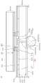
图1示出了例示根据实施方式的半导体封装件的截面图。FIG. 1 shows a cross-sectional view illustrating a semiconductor package according to an embodiment.
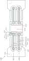
图2示出了例示根据实施方式的半导体封装件的电路互连结构的平面图。FIG. 2 shows a plan view illustrating a circuit interconnection structure of a semiconductor package according to an embodiment.
图3示出了沿图2中的线X2-X2'截取的半导体封装件的截面图。FIG. 3 shows a cross-sectional view of the semiconductor package taken along line X2-X2' in FIG. 2 .
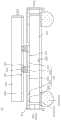
图4示出了沿图2中的线X3-X3'截取的半导体封装件的截面图。FIG. 4 shows a cross-sectional view of the semiconductor package taken along line X3-X3' in FIG. 2 .
图5示出了例示根据实施方式的半导体封装件的电路互连结构的平面图。FIG. 5 shows a plan view illustrating a circuit interconnection structure of a semiconductor package according to an embodiment.
图6示出了例示根据实施方式的半导体封装件的电路互连结构的平面图。FIG. 6 shows a plan view illustrating a circuit interconnection structure of a semiconductor package according to an embodiment.
图7示出了例示根据实施方式的采用包括半导体封装件的存储卡的电子系统的框图。FIG. 7 shows a block diagram illustrating an electronic system employing a memory card including a semiconductor package according to an embodiment.
图8示出了例示根据实施方式的包括半导体封装件的电子系统的框图。FIG. 8 shows a block diagram illustrating an electronic system including a semiconductor package according to an embodiment.
具体实施方式Detailed ways
本文使用的术语可以对应于考虑到它们在实施方式中的功能而选择的词,并且术语的含义可以被解释为根据实施方式所属领域的普通技术人员而不同。如果详细定义,则可以根据定义来解释术语。除非另外定义,否则本文使用的术语(包括技术术语和科学术语)具有与实施方式所属领域的普通技术人员通常理解的含义相同的含义。Terms used herein may correspond to words selected in consideration of their functions in the embodiments, and meanings of the terms may be construed differently depending on those of ordinary skill in the art to which the embodiments pertain. If defined in detail, terms can be interpreted according to the definition. Unless otherwise defined, terms (including technical terms and scientific terms) used herein have the same meaning as commonly understood by one of ordinary skill in the art to which the embodiments belong.
将要理解,尽管术语“第一”、“第二”、“第三”等可以在本文中用于描述各种元件,但这些元件不应受这些术语的限制。这些术语仅用于将一个元件与另一个元件区分开,而不用于暗示或定义元件的特定数量或顺序。It will be understood that although the terms "first", "second", "third", etc. may be used herein to describe various elements, these elements should not be limited by these terms. These terms are only used to distinguish one element from another, and are not used to imply or define a specific number or order of the elements.
还将理解,当元件或层被称为在另一元件或层“上”、“上方”、“下”、“下方”或“外部”时,该元件或层可以是可以存在与该另一元件或层直接接触,或者存在中间的元件或层。用于描述元件或层之间的关系的其他词语应以类似的方式解释(例如,“在...之间”与“直接在...之间”或“相邻”与“直接相邻”)。It will also be understood that when an element or layer is referred to as being "on," "over," "under," "beneath" or "outside" another element or layer, that element or layer can be present with the other element or layer. The elements or layers are in direct contact, or intervening elements or layers may be present. Other words used to describe the relationship between elements or layers should be interpreted in a like fashion (e.g., "between" versus "directly between" or "adjacent" versus "directly adjacent ").
诸如“下方”、“之下”、“下”、“之上”、“上”、“顶”、“底”等的空间相对术语可用于描述元素和/或特征与另一个元素和/或特征的关系,例如,如图所示。应当理解,空间相对术语旨在包括除了图中所示的朝向之外的装置在使用和/或操作中的不同朝向。例如,当翻转图中的装置时,被描述为在另一元素或特征之下或下面的元素然后将定向为在该另一元素或特征之上和/或上面。装置可以以其他方式定向(旋转90度或在其他朝向),并且相应地解释本文使用的空间相对描述符。Spatially relative terms such as "under", "under", "under", "above", "upper", "top", "bottom", etc. may be used to describe the relationship between an element and/or feature and another element and/or feature. The relationship of features, for example, is shown in Fig. It will be understood that the spatially relative terms are intended to encompass different orientations of the device in use and/or operation in addition to the orientation depicted in the figures. For example, when the device in the figures is turned over, elements described as below or below another element or feature would then be oriented above and/or over the other element or feature. The device may be otherwise oriented (rotated 90 degrees or at other orientations) and the spatially relative descriptors used herein interpreted accordingly.
在以下呈现的实施方式中,半导体封装件可以包括电子器件,诸如半导体芯片或半导体管芯。半导体芯片或半导体管芯可以通过使用模切工艺将诸如晶圆之类的半导体基板分离成多个片来获得。半导体芯片可以对应于存储器芯片、逻辑芯片(包括专用集成电路(ASIC)芯片)或片上系统(SoC)。存储器芯片可以包括集成在半导体基板上的动态随机存取存储器(DRAM)电路、静态随机存取存储器(SRAM)电路、NAND型闪存电路、NOR型闪存电路、磁随机存取存储器(MRAM)电路、电阻式随机存取存储器(ReRAM)电路、铁电随机存取存储器(FeRAM)电路或相变随机存取存储器(PcRAM)电路。逻辑芯片可以包括集成在半导体基板上的逻辑电路。半导体封装件可用于诸如移动电话之类的通信系统、与生物技术或医疗保健相关联的电子系统、或可穿戴电子系统中。In the embodiments presented below, a semiconductor package may include an electronic device, such as a semiconductor chip or a semiconductor die. Semiconductor chips or semiconductor dies may be obtained by separating a semiconductor substrate, such as a wafer, into pieces using a die-cutting process. The semiconductor chip may correspond to a memory chip, a logic chip (including an application specific integrated circuit (ASIC) chip), or a system on chip (SoC). The memory chip may include dynamic random access memory (DRAM) circuits, static random access memory (SRAM) circuits, NAND type flash memory circuits, NOR type flash memory circuits, magnetic random access memory (MRAM) circuits, A resistive random access memory (ReRAM) circuit, a ferroelectric random access memory (FeRAM) circuit, or a phase change random access memory (PcRAM) circuit. A logic chip may include logic circuits integrated on a semiconductor substrate. Semiconductor packages may be used in communication systems such as mobile phones, electronic systems associated with biotechnology or healthcare, or wearable electronic systems.
在整个说明书中,相同的附图标记表示相同的元件。即使参照附图没有提及或描述附图标记,也可以参照另一附图提及或描述该附图标记。另外,即使附图中未示出附图标记,也可以参照另一附图来提及或描述该附图标记。Throughout the specification, the same reference numerals denote the same elements. Even if a reference numeral is not mentioned or described with reference to a drawing, it may be mentioned or described with reference to another drawing. In addition, even if a reference numeral is not shown in a drawing, the reference numeral may be mentioned or described with reference to another drawing.
图1示出了例示根据实施方式的半导体封装件10的截面图。图2示出了例示包括在图1的半导体封装件10中的封装基板200S的电路互连结构100的平面图。图1示出了包括沿图2中的线X1-X1'截取的截面图的半导体封装件10的截面图。图3示出了包括沿图2中的线X2-X2'截取的截面图的半导体封装件10的截面图。图4示出了包括沿图2中的线X3-X3'截取的截面图的半导体封装件10的截面图。FIG. 1 shows a cross-sectional view illustrating a
参照图1,半导体封装件10可以被配置为包括封装基板200S和半导体芯片500C。半导体芯片500C可以包括芯片主体500,在芯片主体500中或其上形成集成电路。芯片焊盘510可以设置在芯片主体500的表面501上。芯片焊盘510可以包括将数据信号传输到半导体芯片500C或封装基板200S的信号焊盘,将接地电压传输到半导体芯片500C的接地焊盘以及将电源电压传输到半导体芯片500C的电源焊盘。Referring to FIG. 1 , a
半导体芯片500C可以安装在封装基板200S上。半导体芯片500C可以以倒装芯片形式接合到封装基板200S,使得半导体芯片500C的芯片焊盘510面向封装基板200S。半导体芯片500C可以通过位于半导体芯片500C和封装基板200S之间的内部连接器560电连接到封装基板200S。内部连接器560可以是凸块。钝化层540可以设置在芯片主体500的表面501上以暴露芯片焊盘510。钝化层540可以形成为包括介电层。The
封装基板200S可以是将半导体芯片500C电连接到外部装置(未示出)的互连构件。封装基板200S可以用印刷电路板(PCB)结构来实施。The
封装基板200S可以被配置为包括基板主体200。基板主体200可以包括介电层。基板主体200可以具有第一表面201和第二表面203,半导体芯片500C设置在第一表面201上,第二表面203位于与半导体芯片500C相对。外部连接器600可以附接到基板主体200的第二表面203。外部连接器600可以是用于将半导体封装件10电连接到外部装置的互连构件。外部连接器600可以是互连构件,例如焊球。The
外部连接器着陆部260可以设置在基板主体200的第二表面203上。在这种情况下,外部连接器600可以接合到外部连接器着陆部260。外部连接器着陆部260可以是导电图案。第二介电层430可以设置在基板主体200的第二表面203上,以露出外部连接器着陆部260。第二介电层430可以形成为包括阻焊层。The
导电通孔240可以设置为垂直穿透基板主体200。导电通孔240可以分别电连接到设置在基板主体200的第二表面203上的外部连接器着陆部260。导电通孔240可以分别设置为在平面图中与外部连接器着陆部260交叠。尽管未在图中示出,但是导电连接迹线部可以附加地设置在基板主体200的第二表面203上,以便当导电通孔240被设置为相对于外部连接器着陆部260横向偏移时将导电通孔240电连接至外部连接器着陆部260。The conductive via 240 may be disposed to vertically penetrate the
电路互连结构100可以设置在基板主体200的第一表面201上。电路互连结构100可以包括导电图案。电路互连结构100可以设置为将导电通孔240电连接到内部连接器560。电路互连结构100可以是将导电通孔240电连接到半导体芯片500C的导电图案。第一介电层410可以设置在基板主体200的第一表面201上,以露出电路互连结构100的部分。The
参照图1和图2,设置在基板主体200的第一表面201上的电路互连结构100可以被配置为包括第一焊盘接合部211、第二焊盘接合部212、第三焊盘接合部213、第四焊盘接合部214和第五焊盘接合部215。第一焊盘接合部211、第二焊盘接合部212、第三焊盘接合部213、第四焊盘接合部214和第五焊盘接合部215可以是导电图案。第三焊盘接合部213、第一焊盘接合部211、第二焊盘接合部212、第四焊盘接合部214和第五焊盘接合部215可以顺序排列在与图2的线X1-X1'相交的第一列中。电路互连结构100还可以包括多个第六焊盘接合部217,第六焊盘接合部217可以顺序排列在与第一列间隔开的第二列中。第六焊盘接合部217可以排列成分别面向第三焊盘接合部213、第一焊盘接合部211、第二焊盘接合部212、第四焊盘接合部214和第五焊盘接合部215。Referring to FIGS. 1 and 2 , the
第三焊盘接合部213、第一焊盘接合部211、第二焊盘接合部212、第四焊盘接合部214和第五焊盘接合部215可以分别电连接到半导体芯片500C的相应芯片焊盘510。第六焊盘接合部217也可以分别电连接到半导体芯片500C的相应芯片焊盘510。第三焊盘接合部213、第一焊盘接合部211、第二焊盘接合部212、第四焊盘接合部214和第五焊盘接合部215以及第六焊盘接合部217可以分别位于在平面图中与半导体芯片500C的芯片焊盘510交叠的位置。第三焊盘接合部213、第一焊盘接合部211、第二焊盘接合部212、第四焊盘接合部214和第五焊盘接合部215以及第六焊盘接合部217可以通过内部连接器560分别电连接到半导体芯片500C的芯片焊盘510。The third
第一通孔着陆部231、第二通孔着陆部232、第三通孔着陆部233和第四通孔着陆部234可以设置在基板主体200的第一表面201上,以构成电路互连结构100的一部分。当从平面图观察时,第一通孔着陆部231、第二通孔着陆部232、第三通孔着陆部233和第四通孔着陆部234可以设置为与第一焊盘接合部211、第二焊盘接合部212,第三焊盘接合部213,第四焊盘接合部214,第五焊盘接合部215和第六焊盘接合部217间隔开。第一通孔着陆部231、第二通孔着陆部232、第三通孔着陆部233和第四通孔着陆部234可以设置为在平面图中与导电通孔(图1中的240)交叠。例如,如图1所示,第一通孔着陆部231可以设置为与包括在导电通孔240中的第一导电通孔241交叠,并且可以电连接到第一导电通孔241。The first via
第一连接迹线部251、第二连接迹线部252和第三连接迹线部254以及第一保护迹线部253和第二保护迹线部255可以设置在基板主体200的第一表面201上,以构成电路互连结构100的一部分。第一连接迹线部251、第二连接迹线部252和第三连接迹线部254以及第一保护迹线部253和第二保护迹线部255可以是线形导电图案。The first
第一连接迹线部251可以延伸以将第一焊盘接合部211连接到第一通孔着陆部231。第二连接迹线部252可以连接到第二焊盘接合部212并且可以设置为与第一连接迹线部251平行。第三连接迹线部254可以延伸以将第四焊盘接合部214连接到第四通孔着陆部234。第一连接迹线部251、第二连接迹线部252和第三连接迹线部254可以设置成彼此间隔开一定距离。第一连接迹线部251、第二连接迹线部252和第三连接迹线部254可以延伸为彼此平行。在另一实施方式中,迹线部可以基本彼此平行。基本平行意味着迹线部沿着它们的长度不相交或交叉。The first
第一保护迹线部253可以设置成使得第一保护迹线部253的端部253E与第三焊盘接合部213间隔开并且与第三焊盘接合部213相邻。第一保护迹线部253可以延伸为与第一连接迹线部251平行。第一保护迹线部253可以设置在第一连接迹线部251的与第二连接迹线部252相对的一侧。第一保护迹线部253和第一连接迹线部251可以并排布置以彼此间隔开一定距离。第二保护迹线部255可以设置成使得第二保护迹线部255的端部255E与第五焊盘接合部215间隔开并且与第五焊盘接合部215相邻。第二保护迹线部255可以延伸以与第三连接迹线部254平行。第二保护迹线部255可以设置在第三连接迹线部254的与第二连接迹线部252相对的一侧。The first
第一连接平面部271和第二连接平面部273可以设置在基板主体200的第一表面201上,以构成电路互连结构100的一部分。第一连接平面部271和第二连接平面部273可以是导电图案,它们中的每一个与连接迹线部251、254和保护迹线部253、255相比具有相对大的平面面积。第一连接平面部271和第二连接平面部273可以是与第一通孔着陆部231和第四通孔着陆部234电隔离的导电图案。The first
在实施方式中,第一连接平面部271可以设置为与第一通孔着陆部231间隔开一定距离。第一连接平面部271可以设置为在平面图中部分地围绕第一通孔着陆部231。第一连接平面部271可以延伸以将第二连接迹线部252连接到第一保护迹线部253并且电旁路或绕过第一通孔着陆部231。第一连接平面部271还可以延伸以将第二连接迹线部252连接到第二通孔着陆部232。第一连接平面部271可以是包括第二通孔着陆部232的导电图案。也就是说,第二通孔着陆部232可以对应于第一连接平面部271的一部分。In an embodiment, the first connecting
第一连接平面部271可以附加地延伸以与第四通孔着陆部234间隔开。第一连接平面部271可以延伸以在平面图中部分地围绕并电旁路或绕过第四通孔着陆部234。第一连接平面部271可以延伸以将第二连接迹线部252连接到第二保护迹线部255。第一连接平面部271可以将第一保护迹线部253和第二保护迹线部255电连接到第二通孔着陆部232。The first
第二连接平面部273可以设置成将第三焊盘接合部213连接到第三通孔着陆部233。第二连接平面部273可以被配置为包括第三通孔着陆部233。也就是说,第三通孔着陆部233可以对应于第二连接平面部273的一部分。第二连接平面部273可以延伸以使得第二连接平面部的侧表面273S面向第一焊盘接合部211、第二焊盘接合部212和第四焊盘接合部214。第二连接平面部273还可以延伸以将第五焊盘接合部215连接到第三通孔着陆部233。第二连接平面部273可以设置为与第一焊盘接合部211、第二焊盘接合部212和第四焊盘接合部214间隔开一定距离。例如,第二连接平面部273可以部分地围绕并电旁路或绕过第一焊盘接合部211、第二焊盘接合部212和第四焊盘接合部214,如图2的平面图所示。The second
参照图2,第一保护迹线部253和第二连接迹线部252可以分别位于第一连接迹线部251的两侧。如本文对各种实施方式所使用的,分别位于第三部两侧的第一部和第二部意味着第三部位于第一部和第二部之间。例如,位于第一连接迹线部251两侧的第一保护迹线部253和第二连接迹线部252意味着第一连接迹线部251位于第一保护迹线部253和第二连接迹线部252之间。第二保护迹线部255和第二连接迹线部252可以分别位于第三连接迹线部254的两侧。第一保护迹线部253、第一连接迹线部251、第二连接迹线部252、第三连接迹线部254和第二保护迹线部255可以在与第一列平行的方向上顺序排列。因此,第三焊盘接合部213、第一焊盘接合部211、第二焊盘接合部212、第四焊盘接合部214和第五焊盘接合部215也可以顺序排列在第一列中。Referring to FIG. 2 , the first
第一保护迹线部253和第二连接平面部273可以分别位于第三焊盘接合部213的两侧。另外,第一连接迹线部251和第二连接平面部273可以分别位于第一焊盘接合部211的两侧。因为第一通孔着陆部231连接到第一连接迹线部251并且第三通孔着陆部233连接到第二连接平面部273,所以第一通孔着陆部231和第三通孔着陆部233可以分别位于第一焊盘接合部211的两侧。对于实施方式,第一焊盘接合部211位于第一通孔着陆部231和第三通孔着陆部233之间。The first
第二连接迹线部252和第二连接平面部273可以分别位于第二焊盘接合部212的两侧。因为第二连接迹线部252通过第一连接平面部271连接到第二通孔着陆部232,所以第二通孔着陆部232和第三通孔着陆部233可以分别位于第二焊盘接合部212的两侧。对于实施方式,第二焊盘接合部212位于第二通孔着陆部232和第三通孔着陆部233之间。The second
第二连接平面部273可以位于第一列焊盘接合部和第二列焊盘接合部之间,第一列焊盘接合部包括排列在第一列中的第一焊盘接合部211、第二焊盘接合部212、第三焊盘接合部213、第四焊盘接合部214和第五焊盘接合部215,第二列焊盘接合部包括排列在第二列中的第六焊盘接合部217。因此,第一连接平面部271和第二连接平面部273可以分别位于包括第一焊盘接合部211、第二焊盘接合部212、第三焊盘接合部213、第四焊盘接合部214和第五焊盘接合部215的第一列焊盘接合部的两侧。对于实施方式,其中排列有第一焊盘接合部211、第二焊盘接合部212、第三焊盘接合部213、第四焊盘接合部214和第五焊盘接合部215的第一列位于第一连接平面部271和第二连接平面部273之间。在一些情况下,第一焊盘接合部211、第二焊盘接合部212、第三焊盘接合部213、第四焊盘接合部214和第五焊盘接合部215的第一侧面向或指向第一连接平面部271和第二通孔着陆部232。第一焊盘接合部211、第二焊盘接合部212、第三焊盘接合部213、第四焊盘接合部214和第五焊盘接合部215的第二侧面面向或指向第二连接平面部273和第三通孔着陆部233。The second
参照图1和图2,第一焊盘接合部211、第一连接迹线部251和第一通孔着陆部231可以构成第一数据信号线。第一数据信号线可以是将数据信号传输到半导体芯片500C的信号线。第一数据信号线还可以包括第一导电通孔241、包括在外部连接器着陆部260中的第一外部连接器着陆部261以及包括在外部连接器600中的第一外部连接器601,它们与第一通孔着陆部231串联连接。类似地,第二数据信号线可以包括第四焊盘接合部214、第三连接迹线部254和第四通孔着陆部234。Referring to FIGS. 1 and 2 , the first
参照图2和图3,第二焊盘接合部212、第二连接迹线部252、第一连接平面部271和第二通孔着陆部232可以构成接地线。接地线可以提供用于向半导体芯片500C供应接地电压的电路径。如图4所示,接地线还可以包括导电通孔240中包括的第二导电通孔242、包括在外部连接器着陆部260中的第二外部连接器着陆部262以及包括在外部连接器600中的第二外部连接器602,第二导电通孔242、第二外部连接器着陆部262和第二外部连接器602串联连接到第二通孔着陆部232。第一保护迹线部253和第二保护迹线部255也可以通过第一连接平面部271电连接到接地线以接地。Referring to FIGS. 2 and 3 , the second
参照图2和图4,第三焊盘接合部213、第二连接平面部273和第三通孔着陆部233可以构成第一电源线。第一电源线可以提供用于向半导体芯片500C施加电源电压的电路径。如图3所示,第一电源线还可以包括导电通孔240中包括的第三导电通孔243、包括在外部连接器着陆部260中的第三外部连接器着陆部263以及包括在外部连接器600中的第三外部连接器603,第三导电通孔243、第三外部连接器着陆部263和第三外部连接器603串联连接到第三通孔着陆部233。第五焊盘接合部215、第二连接平面部273和第三通孔着陆部233可以构成第二电源线。Referring to FIGS. 2 and 4 , the third
再次参照图1和图2,数据信号可以通过包括第一焊盘接合部211、第一连接迹线部251、和第一通孔着陆部231的第一数据信号线施加到半导体芯片500C。包括第一连接迹线部251和第一通孔着陆部231的信号路径的阻抗值的变化会影响通过第一连接迹线部251和第一通孔着陆部231传输的数据信号的传输。然而,根据本实施方式,围绕包括第一连接迹线部251和第一通孔着陆部231的电路径的第一保护迹线部253、第一连接平面部271和第二连接迹线部252全部都具有相同的接地电位。因此,可以减轻或抑制包括第一连接迹线部251和第一通孔着陆部231的信号路径的阻抗变化。Referring again to FIGS. 1 and 2 , the data signal may be applied to the
第一保护迹线部253、第一连接平面部271和第二连接迹线部252可以提供围绕第一连接迹线部251和第一通孔着陆部231的连续迹线结构。第一保护迹线部253可以延伸以与第一连接迹线部251平行并且可以连接到第一连接平面部271。第一连接平面部271可以延伸以围绕第一通孔着陆部231并且可以连接到第二连接迹线部252。第二连接迹线部252可以延伸以与第一连接迹线部251平行。因此,第一保护迹线部253、第一连接平面部271和第二连接迹线部252可以串联连接以提供连续迹线结构。The first
如上所述,第一保护迹线部253、第一连接平面部271和第二连接迹线部252全部都可以接地。因此,包括第一保护迹线部253、第一连接平面部271和第二连接迹线部252的结构可以用作包括第一连接迹线部251和第一通孔着陆部231的信号路径的参考平面。因此,包括第一保护迹线部253、第一连接平面部271和第二连接迹线部252的结构可以用作通过包括第一连接迹线部251和第一通孔着陆部231的信号路径传输的数据信号的没有任何不连续区域的连续信号返回路径或者没有任何不连续区域的连续电流返回路径。As described above, all of the first
如上所述,在包括第一保护迹线部253、第一连接平面部271和第二连接迹线部252的结构中不存在任何不连续区域。因此,可以通过包括第一保护迹线部253、第一连接平面部271和第二连接迹线部252的结构的连续性来减轻、抑制或缓和包括第一连接迹线部251和第一通孔着陆部231的信号路径的突然阻抗变化的发生。另外,第一保护迹线部253和第一连接迹线部251可以延伸以彼此相邻并且彼此平行。因此,可以更显著地减轻或抑制包括第一连接迹线部251和第一通孔着陆部231的信号路径的阻抗变化。As described above, there is no discontinuous region in the structure including the first
如果在包括第一保护迹线部253、第一连接平面部271和第二连接迹线部252的结构中存在不连续区域,则不连续区域可能导致包括第一连接迹线部251和第一通孔着陆部231的信号路径的突然阻抗变化。包括第一连接迹线部251和第一通孔着陆部231的信号路径的突然阻抗变化可能影响通过包括第一连接迹线部251和第一通孔着陆部231的信号路径传输的数据信号的传输。也就是说,信号路径的突然阻抗变化可能扰乱通过信号路径传输的数据信号的传输。If there is a discontinuous region in the structure including the first
具有逻辑“高”电平的电源信号可以通过第三焊盘接合部213供应给半导体芯片500C。第一数据信号可以通过第一焊盘接合部211传输。具有逻辑“低”电平的接地信号可以通过第二焊盘接合部212供应给半导体芯片500C。因此,第一焊盘接合部211、第二焊盘接合部212和第三焊盘接合部213可以分别用作电源焊盘、信号焊盘和接地焊盘并且可以设置为彼此相邻。也就是说,第一焊盘接合部211、第二焊盘接合部212和第三焊盘接合部213可以设置为彼此基本上最接近。因此,可以减小施加到半导体芯片500C的电源信号、数据信号和接地信号之间的布线距离,以提高半导体芯片500C的操作速度。A power signal having a logic 'high' level may be supplied to the
用于数据信号、电源信号和接地信号的缓冲电路可以设置在半导体芯片(图1的500C)的芯片主体(图1的500)中或上。缓冲电路可以被配置为执行切换操作。因为电源焊盘、信号焊盘和接地焊盘设置为彼此相邻,所以可以减小连接到缓冲电路的电源线、数据线和接地线的布线距离。因此,可以提高缓冲电路的操作速度。Buffer circuits for data signals, power signals, and ground signals may be provided in or on the chip body (500 of FIG. 1 ) of the semiconductor chip (500C of FIG. 1 ). The buffer circuit may be configured to perform switching operations. Since the power supply pads, signal pads, and ground pads are disposed adjacent to each other, it is possible to reduce the wiring distance of the power supply lines, data lines, and ground lines connected to the buffer circuit. Therefore, the operation speed of the buffer circuit can be increased.
再次参照图2,排列在第二列中的第六焊盘接合部217可以设置为相对于第一列和第二列之间的直线,具有与排列在第一列中的第一焊盘接合部211、第二焊盘接合部212、第三焊盘接合部213、第四焊盘接合部214和第五焊盘接合部215对称的配置。然而,在一些其他实施方式中,第六焊盘接合部217可以随机地设置在任意位置,以具有与第一焊盘接合部211、第二焊盘接合部212、第三焊盘接合部213、第四焊盘接合部214和第五焊盘接合部215不对称的配置。Referring again to FIG. 2 , the sixth
在图2中,尽管第三连接平面部275设置成相对于第一列和第二列之间的直线具有与第一连接平面部271对称的配置,但是根据其他实施方式的第三连接平面部275可以设置成具有与第一连接平面部271不对称的配置。In FIG. 2, although the third
在图2中,尽管第三保护迹线部293和第四保护迹线部295被设置成相对于第一列和第二列之间的直线具有与第一保护迹线部253和第二保护迹线部255对称的配置,但是根据其他实施方式,第三保护迹线部293和第四保护迹线部295可以设置为具有与第一保护迹线部253和第二保护迹线部255不对称的配置。In FIG. 2, although the third
在图2中,尽管第四连接迹线部291、第五连接迹线部292和第六连接迹线部294被设置成相对于第一列和第二列之间的直线具有与第一连接迹线部251、第二连接迹线部252和第三连接迹线部254对称的配置,但是根据其他实施方式,第四连接迹线部291、第五连接迹线部292和第六连接迹线部294可以设置成具有与第一连接迹线部251、第二连接迹线部252和第三连接迹线部254不对称的配置。In FIG. 2, although the fourth
在图2中,尽管第五通孔着陆部281、第六通孔着陆部282和第七通孔着陆部284设置成相对于第一列和第二列之间的直线具有与第一通孔着陆部231、第二通孔着陆部和第四通孔着陆部234对称的配置,但是根据其他实施方式,第五通孔着陆部281、第六通孔着陆部282和第七通孔着陆部284可以设置成具有非对称配置。In FIG. 2, although the fifth through-
图5示出了例示根据实施方式的在半导体封装件中采用的另一电路互连结构1100的平面图。FIG. 5 shows a plan view illustrating another
参照图5,电路互连结构1100可以包括:第一焊盘接合部1211、第二焊盘接合部1212、第三焊盘接合部1213、第四焊盘接合部1214和第五焊盘接合部1215;第一连接迹线部1251、第二连接迹线部1252和第三连接迹线部1254;第一保护迹线部1253和第二保护迹线部1255;第一通孔着陆部1231、第二通孔着陆部1232、第三通孔着陆部1233和第四通孔着陆部1234;以及第一连接平面部1271和第二连接平面部1273。5, the
第一焊盘接合部1211、第一连接迹线部1251和第一通孔着陆部1231可以构成第一数据信号线。第四焊盘接合部1214、第三连接迹线部1254和第四通孔着陆部1234可以构成第二数据信号线。The first
第二焊盘接合部1212、第二连接迹线部1252、第一连接平面部1271和第二通孔着陆部1232可以构成电源线。第一保护迹线部1253和第二保护迹线部1255也可以电连接到第一连接平面部1271,以用作电源线的一部分。当第一数据信号通过第一通孔着陆部1231和第一连接迹线部1251传输时,第一保护迹线部1253、第二连接迹线部1252和第一连接平面部1271可以用作信号返回路径。可以提供第一保护迹线部1253、第二连接迹线部1252和第一连接平面部1271以抑制第一连接迹线部1251的阻抗变化或者减小第一连接迹线部1251的阻抗变化量。当第二数据信号通过第四通孔着陆部1234和第三连接迹线部1254传输时,第二保护迹线部1255、第二连接迹线部1252和第一连接平面部1271可以用作信号返回路径。可以提供第二保护迹线部1255、第二连接迹线部1252和第一连接平面部1271以抑制第三连接迹线部1254的阻抗变化或者减小第三连接迹线部1254的阻抗变化量。The second
第三焊盘接合部1213、第二连接平面部1273和第三通孔着陆部1233可以构成第一接地线。第五焊盘接合部1215、第二连接平面部1273和第三通孔着陆部1233可以构成第二接地线。The third
图6示出了例示根据实施方式的在半导体封装件中采用的又一电路互连结构2100的平面图。FIG. 6 shows a plan view illustrating yet another
参照图6,电路互连结构2100可以包括:第一焊盘接合部2211、第二焊盘接合部2211、第三焊盘接合部2213、第四焊盘接合部2214和第四焊盘接合部2215;第一连接迹线部2251、第二连接迹线部2252和第三连接迹线部2254;第一保护迹线部2253和第二保护迹线部2255;第一通孔着陆部2231、第二通孔着陆部2232、第三通孔着陆部2233和第四通孔着陆部2234;以及第一连接平面部2271和第二连接平面部2273。6, the
第一附加焊盘接合部2218可以连接到第一保护迹线部2253的端部2253E,以面向第三焊盘接合部2213。第一附加焊盘接合部2218可以具有与面向第一附加焊盘接合部2218的第三焊盘接合部2213基本相同的形状。附加的内部连接器(未示出)(例如,具有与内部连接器(图1中的560)相同的形状)可以接合到第一附加焊盘接合部2218。因此,第一附加焊盘接合部2218可以电连接到半导体芯片(图1的500C)。The first additional
第二附加焊盘接合部2219可以连接到第二保护迹线部2255的端部2255E以面向第五焊盘接合部2215。第二附加焊盘接合部2219可以具有与面向第二附加焊盘接合部2219的第五焊盘接合部2215基本相同的形状。附加的内部连接器(未示出)(例如,具有与内部连接器(图1中的560)相同的形状)可以接合到第二附加焊盘接合部2219。因此,第二附加焊盘接合部2219也可以电连接到半导体芯片(图1的500C)。The second additional
图7示出了例示根据本公开的实施方式的包括采用半导体封装件的存储卡7800的电子系统的框图。存储卡7800包括诸如非易失性存储器装置之类的存储器7810以及存储器控制器7820。存储器7810和存储器控制器7820可以存储数据或读出存储的数据。存储器7810和存储器控制器7820中的至少一个可以包括根据实施方式的半导体封装件。FIG. 7 shows a block diagram illustrating an electronic system including a
存储器7810可以包括应用了本公开的实施方式的教导的非易失性存储器装置。存储器控制器7820可以控制存储器7810,以使得响应于来自主机7830的读/写请求而读出存储的数据或将数据进行存储。
图8示出了例示根据本公开的实施方式的包括半导体封装件的电子系统8710的框图。电子系统8710可以包括控制器8711、输入/输出装置8712和存储器8713。控制器8711、输入/输出装置8712和存储器8713可以通过提供数据移动的路径的总线8715彼此联接。FIG. 8 shows a block diagram illustrating an
在实施方式中,控制器8711可以包括微处理器、数字信号处理器、微控制器和/或能够执行与这些组件相同功能的逻辑器件中的一个或更多个。控制器8711和/或存储器8713可以包括根据本公开的实施方式的半导体封装件中的一个或更多个。输入/输出装置8712可以包括从键板、键盘、显示装置、触摸屏等当中选择的至少一个。存储器8713是用于存储数据的装置。存储器8713可以存储要由控制器8711执行的命令和/或数据等。In an embodiment, the
存储器8713可以包括诸如DRAM之类的易失性存储器装置和/或诸如闪存之类的非易失性存储器装置。例如,闪存可以安装到诸如移动终端或台式计算机之类的信息处理系统。闪存可以构成固态盘(SSD)。在这种情况下,电子系统8710可以将大量数据稳定地存储在闪存系统中。
电子系统8710还可以包括接口8714,其被配置为向通信网络发送数据和从通信网络接收数据。接口8714可以是有线类型或无线类型。例如,接口8714可以包括天线或者有线或无线的收发器。
电子系统8710可以实现为移动系统、个人计算机、工业计算机或执行各种功能的逻辑系统。例如,移动系统可以是个人数字助理(PDA)、便携式计算机、平板计算机、移动电话、智能电话、无线电话、膝上型计算机、存储卡、数字音乐系统和信息发送/接收系统中的任何一种。The
如果电子系统8710表示能够执行无线通信的设备,则电子系统8710可以用于使用CDMA(码分多址)、GSM(全球移动通信系统)、NADC(北美数字蜂窝)、E-TDMA(增强时分多址)、WCDMA(宽带码分多址)、CDMA2000、长期演进(LTE)或Wibro(无线宽带互联网)的技术的通信系统中。If
已经出于例示性目的而公开了本公开的有限数量的可能实施方式。本领域技术人员将认识到:在不背离本公开和所附权利要求的范围和精神的情况下,对于所呈现的实施方式,可以进行各种修改、添加和替换。A limited number of possible implementations of the present disclosure have been disclosed for illustrative purposes. Those skilled in the art will appreciate that various modifications, additions and substitutions can be made to the presented embodiments without departing from the scope and spirit of the disclosure and appended claims.
相关申请的交叉引用Cross References to Related Applications
本申请要求于2018年12月3日递交的韩国申请No.10-2018-0153938的优先权,其全部内容通过引用并入本文。This application claims priority from Korean Application No. 10-2018-0153938 filed on December 3, 2018, the entire contents of which are incorporated herein by reference.
Claims (27)
Translated fromChineseApplications Claiming Priority (2)
| Application Number | Priority Date | Filing Date | Title |
|---|---|---|---|
| KR10-2018-0153938 | 2018-12-03 | ||
| KR1020180153938AKR102620865B1 (en) | 2018-12-03 | 2018-12-03 | Semiconductor package |
Publications (2)
| Publication Number | Publication Date |
|---|---|
| CN111261605A CN111261605A (en) | 2020-06-09 |
| CN111261605Btrue CN111261605B (en) | 2023-04-07 |
Family
ID=70681391
Family Applications (1)
| Application Number | Title | Priority Date | Filing Date |
|---|---|---|---|
| CN201911099388.4AActiveCN111261605B (en) | 2018-12-03 | 2019-11-12 | Semiconductor package |
Country Status (5)
| Country | Link |
|---|---|
| US (1) | US10998281B2 (en) |
| KR (1) | KR102620865B1 (en) |
| CN (1) | CN111261605B (en) |
| DE (1) | DE102019129642B4 (en) |
| TW (1) | TWI819060B (en) |
Families Citing this family (5)
| Publication number | Priority date | Publication date | Assignee | Title |
|---|---|---|---|---|
| KR102620865B1 (en) | 2018-12-03 | 2024-01-04 | 에스케이하이닉스 주식회사 | Semiconductor package |
| KR102538705B1 (en)* | 2018-12-04 | 2023-06-01 | 에스케이하이닉스 주식회사 | Semiconductor package |
| US11848261B2 (en)* | 2020-10-08 | 2023-12-19 | Ciena Corporation | Low RF crosstalk devices via a slot for isolation |
| US12021515B2 (en)* | 2020-11-30 | 2024-06-25 | SK Hynix Inc. | Semiconductor chip including chip pads of different surface areas, and semiconductor package including the semiconductor chip |
| CN112885808B (en)* | 2021-01-21 | 2022-03-08 | 长鑫存储技术有限公司 | Packaging substrate and packaging structure |
Citations (14)
| Publication number | Priority date | Publication date | Assignee | Title |
|---|---|---|---|---|
| US5686764A (en)* | 1996-03-20 | 1997-11-11 | Lsi Logic Corporation | Flip chip package with reduced number of package layers |
| US5691568A (en)* | 1996-05-31 | 1997-11-25 | Lsi Logic Corporation | Wire bondable package design with maxium electrical performance and minimum number of layers |
| US5994766A (en)* | 1998-09-21 | 1999-11-30 | Vlsi Technology, Inc. | Flip chip circuit arrangement with redistribution layer that minimizes crosstalk |
| US6008534A (en)* | 1998-01-14 | 1999-12-28 | Lsi Logic Corporation | Integrated circuit package having signal traces interposed between power and ground conductors in order to form stripline transmission lines |
| JP2001024084A (en)* | 1999-07-09 | 2001-01-26 | Nec Corp | Area array type semiconductor device |
| GB0110895D0 (en)* | 2000-06-09 | 2001-06-27 | Samsung Electronics Co Ltd | Ball grid array package semiconductor device having improved power line routing |
| US6462423B1 (en)* | 2000-08-31 | 2002-10-08 | Micron Technology, Inc. | Flip-chip with matched lines and ground plane |
| US6608376B1 (en)* | 2002-03-25 | 2003-08-19 | Lsi Logic Corporation | Integrated circuit package substrate with high density routing mechanism |
| US6776659B1 (en)* | 2003-06-26 | 2004-08-17 | Teradyne, Inc. | High speed, high density electrical connector |
| GB0501210D0 (en)* | 2005-01-21 | 2005-03-02 | Artimi Ltd | Integrated circuit die connection methods and apparatus |
| US6891260B1 (en)* | 2002-06-06 | 2005-05-10 | Lsi Logic Corporation | Integrated circuit package substrate with high density routing mechanism |
| WO2011047479A1 (en)* | 2009-10-23 | 2011-04-28 | Ati Technologies Ulc | A routing layer for mitigating stress in a semiconductor die |
| CN106601717A (en)* | 2015-10-19 | 2017-04-26 | 爱思开海力士有限公司 | Semiconductor chip module and semiconductor package including the same |
| CN107316853A (en)* | 2016-04-26 | 2017-11-03 | 爱思开海力士有限公司 | Semiconductor package part |
Family Cites Families (26)
| Publication number | Priority date | Publication date | Assignee | Title |
|---|---|---|---|---|
| JP2786165B2 (en)* | 1996-06-19 | 1998-08-13 | 甲府日本電気株式会社 | Card edge connector for printed wiring board and method of manufacturing the same |
| KR100348820B1 (en)* | 2000-12-28 | 2002-08-17 | 삼성전자 주식회사 | High frequency semiconductor chip package and a board using in the package |
| SG142115A1 (en)* | 2002-06-14 | 2008-05-28 | Micron Technology Inc | Wafer level packaging |
| US7550842B2 (en)* | 2002-12-12 | 2009-06-23 | Formfactor, Inc. | Integrated circuit assembly |
| WO2005048307A2 (en)* | 2003-11-08 | 2005-05-26 | Chippac, Inc. | Flip chip interconnection pad layout |
| US8853001B2 (en)* | 2003-11-08 | 2014-10-07 | Stats Chippac, Ltd. | Semiconductor device and method of forming pad layout for flipchip semiconductor die |
| US8574959B2 (en)* | 2003-11-10 | 2013-11-05 | Stats Chippac, Ltd. | Semiconductor device and method of forming bump-on-lead interconnection |
| US7030712B2 (en)* | 2004-03-01 | 2006-04-18 | Belair Networks Inc. | Radio frequency (RF) circuit board topology |
| US8120927B2 (en) | 2008-04-07 | 2012-02-21 | Mediatek Inc. | Printed circuit board |
| US7994871B2 (en) | 2008-06-30 | 2011-08-09 | Himax Technologies Limited | Chip on film trace routing method for electrical magnetic interference reduction |
| KR101535223B1 (en) | 2008-08-18 | 2015-07-09 | 삼성전자주식회사 | Tape circuit boards, chip-on-film packages and device assemblies |
| KR101632399B1 (en)* | 2009-10-26 | 2016-06-23 | 삼성전자주식회사 | Semiconductor and method for fabricating the same |
| US9159777B2 (en)* | 2011-04-15 | 2015-10-13 | Infineon Technologies Ag | Die arrangements containing an inductor coil and methods of manufacturing a die arrangement containing an inductor coil |
| US8723337B2 (en)* | 2011-07-14 | 2014-05-13 | Texas Instruments Incorporated | Structure for high-speed signal integrity in semiconductor package with single-metal-layer substrate |
| KR102041243B1 (en)* | 2013-04-26 | 2019-11-07 | 삼성전자주식회사 | Semiconductor package |
| US10163767B2 (en)* | 2013-10-11 | 2018-12-25 | Mediatek Inc. | Semiconductor package |
| TWI572256B (en) | 2014-01-09 | 2017-02-21 | 上海兆芯集成電路有限公司 | Circuit board and electronic assembely |
| TWM485516U (en)* | 2014-05-07 | 2014-09-01 | Ttop Corp | LED frame structure |
| JP6272173B2 (en)* | 2014-07-31 | 2018-01-31 | 京セラ株式会社 | Wiring board |
| US9609749B2 (en) | 2014-11-14 | 2017-03-28 | Mediatek Inc. | Printed circuit board having power/ground ball pad array |
| US9659863B2 (en)* | 2014-12-01 | 2017-05-23 | Taiwan Semiconductor Manufacturing Company, Ltd. | Semiconductor devices, multi-die packages, and methods of manufacture thereof |
| US10276519B2 (en)* | 2015-06-02 | 2019-04-30 | Sarcina Technology LLC | Package substrate differential impedance optimization for 25 to 60 Gbps and beyond |
| KR102437687B1 (en) | 2015-11-10 | 2022-08-26 | 삼성전자주식회사 | Semiconductor devices and semicinductor packages thereof |
| KR20170067947A (en)* | 2015-12-08 | 2017-06-19 | 에스케이하이닉스 주식회사 | Semiconductor package including side shielding and method for fabricating the same |
| KR102737499B1 (en)* | 2016-12-16 | 2024-12-05 | 삼성전자주식회사 | Semiconductor device including overlay patterns |
| KR102620865B1 (en) | 2018-12-03 | 2024-01-04 | 에스케이하이닉스 주식회사 | Semiconductor package |
- 2018
- 2018-12-03KRKR1020180153938Apatent/KR102620865B1/enactiveActive
- 2019
- 2019-08-12TWTW108128579Apatent/TWI819060B/enactive
- 2019-08-13USUS16/539,602patent/US10998281B2/enactiveActive
- 2019-11-04DEDE102019129642.0Apatent/DE102019129642B4/enactiveActive
- 2019-11-12CNCN201911099388.4Apatent/CN111261605B/enactiveActive
Patent Citations (14)
| Publication number | Priority date | Publication date | Assignee | Title |
|---|---|---|---|---|
| US5686764A (en)* | 1996-03-20 | 1997-11-11 | Lsi Logic Corporation | Flip chip package with reduced number of package layers |
| US5691568A (en)* | 1996-05-31 | 1997-11-25 | Lsi Logic Corporation | Wire bondable package design with maxium electrical performance and minimum number of layers |
| US6008534A (en)* | 1998-01-14 | 1999-12-28 | Lsi Logic Corporation | Integrated circuit package having signal traces interposed between power and ground conductors in order to form stripline transmission lines |
| US5994766A (en)* | 1998-09-21 | 1999-11-30 | Vlsi Technology, Inc. | Flip chip circuit arrangement with redistribution layer that minimizes crosstalk |
| JP2001024084A (en)* | 1999-07-09 | 2001-01-26 | Nec Corp | Area array type semiconductor device |
| GB0110895D0 (en)* | 2000-06-09 | 2001-06-27 | Samsung Electronics Co Ltd | Ball grid array package semiconductor device having improved power line routing |
| US6462423B1 (en)* | 2000-08-31 | 2002-10-08 | Micron Technology, Inc. | Flip-chip with matched lines and ground plane |
| US6608376B1 (en)* | 2002-03-25 | 2003-08-19 | Lsi Logic Corporation | Integrated circuit package substrate with high density routing mechanism |
| US6891260B1 (en)* | 2002-06-06 | 2005-05-10 | Lsi Logic Corporation | Integrated circuit package substrate with high density routing mechanism |
| US6776659B1 (en)* | 2003-06-26 | 2004-08-17 | Teradyne, Inc. | High speed, high density electrical connector |
| GB0501210D0 (en)* | 2005-01-21 | 2005-03-02 | Artimi Ltd | Integrated circuit die connection methods and apparatus |
| WO2011047479A1 (en)* | 2009-10-23 | 2011-04-28 | Ati Technologies Ulc | A routing layer for mitigating stress in a semiconductor die |
| CN106601717A (en)* | 2015-10-19 | 2017-04-26 | 爱思开海力士有限公司 | Semiconductor chip module and semiconductor package including the same |
| CN107316853A (en)* | 2016-04-26 | 2017-11-03 | 爱思开海力士有限公司 | Semiconductor package part |
Also Published As
| Publication number | Publication date |
|---|---|
| CN111261605A (en) | 2020-06-09 |
| TWI819060B (en) | 2023-10-21 |
| DE102019129642B4 (en) | 2025-03-27 |
| DE102019129642A1 (en) | 2020-06-04 |
| TW202023015A (en) | 2020-06-16 |
| KR20200067051A (en) | 2020-06-11 |
| US20200176406A1 (en) | 2020-06-04 |
| US10998281B2 (en) | 2021-05-04 |
| KR102620865B1 (en) | 2024-01-04 |
Similar Documents
| Publication | Publication Date | Title |
|---|---|---|
| CN111261605B (en) | Semiconductor package | |
| CN111490029B (en) | Semiconductor package including bridged die | |
| CN108933110B (en) | Semiconductor package including stacked chips | |
| US10903131B2 (en) | Semiconductor packages including bridge die spaced apart from semiconductor die | |
| CN110875296A (en) | Package-on-package including bridge die | |
| US10553567B2 (en) | Chip stack packages | |
| CN112786565A (en) | Package-on-package with interposer bridge | |
| CN111276458B (en) | Semiconductor package | |
| US12131997B2 (en) | Semiconductor packages | |
| US11715708B2 (en) | Semiconductor package including decoupling capacitor | |
| US20190237398A1 (en) | Semiconductor packages | |
| CN114582816A (en) | Semiconductor package including heat dissipation layer | |
| US9543251B2 (en) | Semiconductor chip and semiconductor package having the same | |
| CN113257787B (en) | Semiconductor package including chips stacked on a base module | |
| US11322475B2 (en) | Stack semiconductor packages having wire-bonding connection structure | |
| US12199061B2 (en) | Semiconductor packages | |
| KR102188644B1 (en) | Semiconductor package having extanded bandwidth | |
| US20230056222A1 (en) | Semiconductor packages | |
| KR102487532B1 (en) | Semiconductor chip and stacked semiconductor chip using the same |
Legal Events
| Date | Code | Title | Description |
|---|---|---|---|
| PB01 | Publication | ||
| PB01 | Publication | ||
| SE01 | Entry into force of request for substantive examination | ||
| SE01 | Entry into force of request for substantive examination | ||
| GR01 | Patent grant | ||
| GR01 | Patent grant |