CN111259014B - A single-way linked list data storage method and system for FPGA - Google Patents
A single-way linked list data storage method and system for FPGADownload PDFInfo
- Publication number
- CN111259014B CN111259014BCN202010079637.XACN202010079637ACN111259014BCN 111259014 BCN111259014 BCN 111259014BCN 202010079637 ACN202010079637 ACN 202010079637ACN 111259014 BCN111259014 BCN 111259014B
- Authority
- CN
- China
- Prior art keywords
- linked list
- data
- chip
- fpga
- data packet
- Prior art date
- Legal status (The legal status is an assumption and is not a legal conclusion. Google has not performed a legal analysis and makes no representation as to the accuracy of the status listed.)
- Active
Links
Images

Classifications
- G—PHYSICS
- G06—COMPUTING OR CALCULATING; COUNTING
- G06F—ELECTRIC DIGITAL DATA PROCESSING
- G06F16/00—Information retrieval; Database structures therefor; File system structures therefor
- G06F16/20—Information retrieval; Database structures therefor; File system structures therefor of structured data, e.g. relational data
- G06F16/22—Indexing; Data structures therefor; Storage structures
- G06F16/2228—Indexing structures
- G—PHYSICS
- G06—COMPUTING OR CALCULATING; COUNTING
- G06F—ELECTRIC DIGITAL DATA PROCESSING
- G06F15/00—Digital computers in general; Data processing equipment in general
- G06F15/76—Architectures of general purpose stored program computers
- G06F15/78—Architectures of general purpose stored program computers comprising a single central processing unit
- G06F15/7807—System on chip, i.e. computer system on a single chip; System in package, i.e. computer system on one or more chips in a single package
- G06F15/781—On-chip cache; Off-chip memory
- G—PHYSICS
- G06—COMPUTING OR CALCULATING; COUNTING
- G06F—ELECTRIC DIGITAL DATA PROCESSING
- G06F15/00—Digital computers in general; Data processing equipment in general
- G06F15/76—Architectures of general purpose stored program computers
- G06F15/78—Architectures of general purpose stored program computers comprising a single central processing unit
- G06F15/7867—Architectures of general purpose stored program computers comprising a single central processing unit with reconfigurable architecture
- G06F15/7871—Reconfiguration support, e.g. configuration loading, configuration switching, or hardware OS
- G—PHYSICS
- G06—COMPUTING OR CALCULATING; COUNTING
- G06F—ELECTRIC DIGITAL DATA PROCESSING
- G06F16/00—Information retrieval; Database structures therefor; File system structures therefor
- G06F16/20—Information retrieval; Database structures therefor; File system structures therefor of structured data, e.g. relational data
- G06F16/24—Querying
- G06F16/245—Query processing
- G06F16/2455—Query execution
- G06F16/24552—Database cache management
- G—PHYSICS
- G06—COMPUTING OR CALCULATING; COUNTING
- G06F—ELECTRIC DIGITAL DATA PROCESSING
- G06F16/00—Information retrieval; Database structures therefor; File system structures therefor
- G06F16/20—Information retrieval; Database structures therefor; File system structures therefor of structured data, e.g. relational data
- G06F16/24—Querying
- G06F16/245—Query processing
- G06F16/24569—Query processing with adaptation to specific hardware, e.g. adapted for using GPUs or SSDs
- G—PHYSICS
- G06—COMPUTING OR CALCULATING; COUNTING
- G06F—ELECTRIC DIGITAL DATA PROCESSING
- G06F3/00—Input arrangements for transferring data to be processed into a form capable of being handled by the computer; Output arrangements for transferring data from processing unit to output unit, e.g. interface arrangements
- G06F3/06—Digital input from, or digital output to, record carriers, e.g. RAID, emulated record carriers or networked record carriers
- G06F3/0601—Interfaces specially adapted for storage systems
- G06F3/0602—Interfaces specially adapted for storage systems specifically adapted to achieve a particular effect
- G06F3/0625—Power saving in storage systems
- G—PHYSICS
- G06—COMPUTING OR CALCULATING; COUNTING
- G06F—ELECTRIC DIGITAL DATA PROCESSING
- G06F3/00—Input arrangements for transferring data to be processed into a form capable of being handled by the computer; Output arrangements for transferring data from processing unit to output unit, e.g. interface arrangements
- G06F3/06—Digital input from, or digital output to, record carriers, e.g. RAID, emulated record carriers or networked record carriers
- G06F3/0601—Interfaces specially adapted for storage systems
- G06F3/0628—Interfaces specially adapted for storage systems making use of a particular technique
- G06F3/0629—Configuration or reconfiguration of storage systems
- G06F3/0631—Configuration or reconfiguration of storage systems by allocating resources to storage systems
- G—PHYSICS
- G06—COMPUTING OR CALCULATING; COUNTING
- G06F—ELECTRIC DIGITAL DATA PROCESSING
- G06F3/00—Input arrangements for transferring data to be processed into a form capable of being handled by the computer; Output arrangements for transferring data from processing unit to output unit, e.g. interface arrangements
- G06F3/06—Digital input from, or digital output to, record carriers, e.g. RAID, emulated record carriers or networked record carriers
- G06F3/0601—Interfaces specially adapted for storage systems
- G06F3/0628—Interfaces specially adapted for storage systems making use of a particular technique
- G06F3/0655—Vertical data movement, i.e. input-output transfer; data movement between one or more hosts and one or more storage devices
- G06F3/0656—Data buffering arrangements
Landscapes
- Engineering & Computer Science (AREA)
- Theoretical Computer Science (AREA)
- General Engineering & Computer Science (AREA)
- General Physics & Mathematics (AREA)
- Physics & Mathematics (AREA)
- Computer Hardware Design (AREA)
- Databases & Information Systems (AREA)
- Data Mining & Analysis (AREA)
- Human Computer Interaction (AREA)
- Computational Linguistics (AREA)
- Computing Systems (AREA)
- Microelectronics & Electronic Packaging (AREA)
- Software Systems (AREA)
- Logic Circuits (AREA)
Abstract
Description
Translated fromChinese技术领域technical field
本发明属于芯片数据流控技术领域,具体涉及一种FPGA的单向链表数据存储方法及系统。The invention belongs to the technical field of chip data flow control, and in particular relates to a data storage method and system of a one-way linked list of FPGA.
背景技术Background technique
链表是一种数据结构,在内存中通过节点记录内存地址而相互链接形成一条链的储存方式。相比数组而言,链表在内存中不需要连续的区域,只需要每一个节点都能够记录下一个节点的内存地址,通过引用进行查找,这样的特点也就造就了链表增删操作时间消耗很小,而查找遍历时间消耗很大的特点。A linked list is a data structure that is stored in memory through nodes that record memory addresses and are linked to each other to form a chain. Compared with an array, a linked list does not require a continuous area in the memory. It only needs that each node can record the memory address of the next node and search it by reference. , and the search traversal time consumes a lot of features.
FPGA具有速度快、效率高、灵活稳定、集成度高等优点,所以在硬件逻辑验证与设计中是十分必要的,目前FPGA芯片内经常需要缓存一些管理数据包,数据包内包含FPGA芯片需要读取的数据和数据包的配置信息,PPGA芯片主要包含了可编程逻辑模块、固定功能逻辑模块(如乘法器)的数目及存储器(如嵌入式RAM),其中,FPGA的基本可编程逻辑单元是由查找表和寄存器组成的。FPGA has the advantages of fast speed, high efficiency, flexibility and stability, and high integration, so it is very necessary in hardware logic verification and design. At present, FPGA chips often need to cache some management data packets, and the data packets contain FPGA chips that need to be read. The configuration information of the data and data packets, the PPGA chip mainly includes the number of programmable logic modules, fixed function logic modules (such as multipliers) and memory (such as embedded RAM), among which, the basic programmable logic unit of FPGA is composed of consists of lookup tables and registers.
现有技术FPGA读取时存在以下缺陷:FPGA片内的缓存小,不能在片内存储大量数据;FPGA片外的缓存大,但是片内模块不方便直接管理片外的缓存数据;FPGA 在应用时并行操作较多,但是提高工作效率一般,直接读取数据时会降低CPU的效率。The prior art FPGA has the following defects when reading: the cache in the FPGA chip is small, and a large amount of data cannot be stored in the chip; the cache outside the FPGA chip is large, but the on-chip module is inconvenient to directly manage the cache data outside the chip; There are many parallel operations, but the work efficiency is generally improved, and the efficiency of the CPU will be reduced when directly reading data.
发明内容Contents of the invention
针对现有技术的上述不足,本发明提供一种FPGA的单向链表数据存储方法及系统,以解决上述技术问题。Aiming at the above-mentioned deficiencies of the prior art, the present invention provides an FPGA singly linked list data storage method and system to solve the above-mentioned technical problems.
第一方面,本发明提供一种FPGA的单向链表数据存储方法,包括:In the first aspect, the present invention provides a kind of one-way linked list data storage method of FPGA, comprising:
将片内RAM和片外DDR均划分为多个节点,将片内RAM节点和片外DDR节点依次构建成FPGA的单向链表,并设置节点的指针;Divide the on-chip RAM and off-chip DDR into multiple nodes, build the on-chip RAM nodes and off-chip DDR nodes into a one-way linked list of FPGA in turn, and set the pointers of the nodes;
将FPGA的寄存器地址配置为单向链表的索引地址;Configure the FPGA register address as the index address of the singly linked list;
将数据包的配置信息缓存到片内RAM节点,所述数据包的数据缓存到片外 DDR节点。The configuration information of the data packet is cached to the on-chip RAM node, and the data of the data packet is cached to the off-chip DDR node.
进一步的,所述方法还包括:Further, the method also includes:
根据FPGA的存储数据读取指令获取寄存器地址;Obtain the register address according to the FPGA storage data read instruction;
根据所述寄存器地址索引到待测数据包所在的RAM节点,并读取待测数据包的配置信息;Index to the RAM node where the data packet to be tested is located according to the register address, and read the configuration information of the data packet to be tested;
根据片内RAM节点的指针索引到片外DDR节点,并读取待测数据包的数据。Index to the off-chip DDR node according to the pointer of the on-chip RAM node, and read the data of the data packet to be tested.
进一步的,所述方法还包括:Further, the method also includes:
CPU通过总线读取待测数据包的配置信息;The CPU reads the configuration information of the data packet to be tested through the bus;
DAM通过DMA交互模块读取待测数据包的数据。The DAM reads the data of the data packet to be tested through the DMA interaction module.
进一步的,所述方法还包括:Further, the method also includes:
将所述单向链表的第一个片内RAM节点配置为链表头;Configuring the first on-chip RAM node of the one-way linked list as a linked list head;
所述链表头内输入链表配置信息。The linked list configuration information is input in the linked list header.
进一步的,所述数据配置信息包括:数据包大小、数据包数量、数据包是否校验信息和数据校验位。Further, the data configuration information includes: data packet size, data packet quantity, data packet check information and data check digit.
进一步的,所述链表配置信息包括的单向链表的数据类型,传输通道,优先级,路由信息和目的地址。Further, the linked list configuration information includes the data type of the one-way linked list, transmission channel, priority, routing information and destination address.
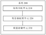
第二方面,本发明提供一种FPGA的单向链表数据存储系统,包括:Second aspect, the present invention provides a kind of one-way linked list data storage system of FPGA, comprises:
结构分配单元,配置用于将片内RAM和片外DDR均划分为多个节点,将片内RAM节点和片外DDR节点依次构建成FPGA的单向链表,并设置节点的指针;The structure allocation unit is configured to divide the on-chip RAM and the off-chip DDR into multiple nodes, construct the on-chip RAM nodes and the off-chip DDR nodes into a one-way linked list of FPGA in turn, and set the pointers of the nodes;
寄存器配置单元,配置用于将FPGA的寄存器地址配置为单向链表的索引地址;The register configuration unit is configured to configure the register address of the FPGA as the index address of the one-way linked list;
数据存储单元,配置用于将数据包的配置信息缓存到片内RAM节点,所述数据包的数据缓存到片外DDR节点。The data storage unit is configured to cache the configuration information of the data packet to the on-chip RAM node, and cache the data of the data packet to the off-chip DDR node.
进一步的,所述系统还包括:Further, the system also includes:
读取指令单元,配置用于根据FPGA的存储数据读取指令获取寄存器地址;A read instruction unit configured to obtain a register address according to an FPGA stored data read instruction;
地址索引单元,配置用于根据所述寄存器地址索引到待测数据包所在的片内RAM节点,并读取待测数据包的配置信息;The address index unit is configured to index to the on-chip RAM node where the data packet to be tested is located according to the register address, and read the configuration information of the data packet to be tested;
数据读取单元,配置用于根据片内RAM节点的指针索引到片外DDR节点,并读取待测数据包的数据。The data reading unit is configured to index to the off-chip DDR node according to the pointer of the on-chip RAM node, and read the data of the data packet to be tested.
进一步的,所述系统还包括:Further, the system also includes:
表头配置单元,配置用于将所述单向链表的第一个片内RAM节点配置为链表头;A header configuration unit configured to configure the first on-chip RAM node of the one-way linked list as a linked list header;
表头信息输入单元,配置用于所述链表头内输入链表配置信息。The header information input unit is configured for inputting configuration information of the linked list in the linked list header.
本发明的有益效果在于:The beneficial effects of the present invention are:
本发明提供的一种FPGA的单向链表数据存储方法及系统,构建了单向链表形式的内存节点,在片内RAM节点上获取配置信息,节省了配置信息对寄存器的资源占用,解决了单模块寄存器资源紧张的问题;采用链表的方式形成流水线操作,每个节点即阶段,执行不同的操作,并且按照顺序自动执行,提高了数据读取的工作效率;采用链表结合硬件结构的方式,对缓存空间采用分布式节点分布式,占用资源多的数据部分缓存到片外DDR内,极大地降低了片内资源的消耗;通过DMA读取片外DDR内缓存的数据,减少了CPU的工作负担。A method and system for storing data in a one-way linked list of an FPGA provided by the present invention constructs a memory node in the form of a one-way linked list, obtains configuration information on the on-chip RAM node, saves the resource occupation of the register by the configuration information, and solves the problem of single The problem of shortage of module register resources; use the linked list to form a pipeline operation, each node is a stage, perform different operations, and execute them automatically in order, which improves the work efficiency of data reading; use the linked list combined with the hardware structure, for The cache space is distributed by distributed nodes, and the data that takes up a lot of resources is partially cached in the off-chip DDR, which greatly reduces the consumption of on-chip resources; the data cached in the off-chip DDR is read through DMA, reducing the workload of the CPU .
此外,本发明设计原理可靠,结构简单,具有非常广泛的应用前景。In addition, the design principle of the present invention is reliable, the structure is simple, and has very wide application prospects.
附图说明Description of drawings
为了更清楚地说明本发明实施例或现有技术中的技术方案,下面将对实施例或现有技术描述中所需要使用的附图作简单地介绍,显而易见地,对于本领域普通技术人员而言,在不付出创造性劳动的前提下,还可以根据这些附图获得其他的附图。In order to more clearly illustrate the technical solutions in the embodiments of the present invention or the prior art, the following will briefly introduce the drawings that need to be used in the description of the embodiments or the prior art. Obviously, for those of ordinary skill in the art, In other words, other drawings can also be obtained from these drawings on the premise of not paying creative work.
图1是本发明一个实施例的方法的示意性流程图。Fig. 1 is a schematic flowchart of a method according to an embodiment of the present invention.
图2是本发明一个实施例的系统的示意性框图。Fig. 2 is a schematic block diagram of a system according to one embodiment of the present invention.
具体实施方式detailed description
为了使本技术领域的人员更好地理解本发明中的技术方案,下面将结合本发明实施例中的附图,对本发明实施例中的技术方案进行清楚、完整地描述,显然,所描述的实施例仅仅是本发明一部分实施例,而不是全部的实施例。基于本发明中的实施例,本领域普通技术人员在没有做出创造性劳动前提下所获得的所有其他实施例,都应当属于本发明保护的范围。In order to enable those skilled in the art to better understand the technical solutions in the present invention, the technical solutions in the embodiments of the present invention will be clearly and completely described below in conjunction with the drawings in the embodiments of the present invention. Obviously, the described The embodiments are only some of the embodiments of the present invention, not all of them. Based on the embodiments of the present invention, all other embodiments obtained by persons of ordinary skill in the art without making creative efforts shall fall within the protection scope of the present invention.
下面对本发明中出现的关键术语进行解释。Key terms appearing in the present invention are explained below.
DDR:双倍速率同步动态随机存储器。DDR: Double Rate Synchronous Dynamic Random Access Memory.
图1是本发明一个实施例的方法的示意性流程图。其中,图1执行主体可以为一种FPGA的单向链表数据存储系统。Fig. 1 is a schematic flowchart of a method according to an embodiment of the present invention. Wherein, the execution subject in FIG. 1 may be a single-way linked list data storage system of FPGA.
如图1所示,该方法100包括:As shown in Figure 1, the method 100 includes:
步骤110,将片内RAM和片外DDR均划分为多个节点,将片内RAM节点和片外DDR节点依次构建成FPGA的单向链表,并设置节点的指针;
步骤120,将FPGA的寄存器地址配置为单向链表的索引地址;
步骤130,将数据包的配置信息缓存到片内RAM节点,所述数据包的数据缓存到片外DDR节点。
可选地,作为本发明一个实施例,所述方法还包括:Optionally, as an embodiment of the present invention, the method further includes:
根据FPGA的存储数据读取指令获取寄存器地址;Obtain the register address according to the FPGA storage data read instruction;
根据所述寄存器地址索引到待测数据包所在的RAM节点,并读取待测数据包的配置信息;Index to the RAM node where the data packet to be tested is located according to the register address, and read the configuration information of the data packet to be tested;
根据片内RAM节点的指针索引到片外DDR节点,并读取待测数据包的数据。Index to the off-chip DDR node according to the pointer of the on-chip RAM node, and read the data of the data packet to be tested.
可选地,作为本发明一个实施例,所述方法还包括:Optionally, as an embodiment of the present invention, the method further includes:
CPU通过总线读取待测数据包的配置信息;The CPU reads the configuration information of the data packet to be tested through the bus;
DAM通过DMA交互模块读取待测数据包的数据。The DAM reads the data of the data packet to be tested through the DMA interaction module.
可选地,作为本发明一个实施例,所述方法还包括:Optionally, as an embodiment of the present invention, the method further includes:
将所述单向链表的第一个片内RAM节点配置为链表头;Configuring the first on-chip RAM node of the one-way linked list as a linked list head;
所述链表头内输入链表配置信息。The linked list configuration information is input in the linked list header.
可选地,作为本发明一个实施例,所述数据配置信息包括:数据包大小、数据包数量、数据包是否校验信息和数据校验位。Optionally, as an embodiment of the present invention, the data configuration information includes: data packet size, data packet quantity, data packet check information, and data check bits.
进一步的,所述链表配置信息包括的单向链表的数据类型,传输通道,优先级,路由信息和目的地址。Further, the linked list configuration information includes the data type of the one-way linked list, transmission channel, priority, routing information and destination address.
为了便于对本发明的理解,下面以本发明一种FPGA的单向链表数据存储方法的原理,结合实施例中对一种FPGA内存进行管理的过程,对本发明提供的一种FPGA的单向链表数据存储方法做进一步的描述。In order to facilitate the understanding of the present invention, below with the principle of a kind of FPGA single-way linked list data storage method of the present invention, in conjunction with the process that a kind of FPGA memory is managed in the embodiment, the one-way linked list data of a kind of FPGA provided by the present invention Storage methods are described further.
具体的,所述FPGA的单向链表数据存储方法包括:Concrete, the one-way linked list data storage method of described FPGA comprises:
S1、将片内RAM和片外DDR均划分为多个节点,将片内RAM节点和片外DDR 节点依次构建成FPGA的单向链表,并设置节点的指针;S1, on-chip RAM and off-chip DDR are all divided into a plurality of nodes, and on-chip RAM node and off-chip DDR node are built into the singly linked list of FPGA successively, and the pointer of node is set;
为增大FPGA芯片外的片外DDR FPGA芯片内的片内RAM和,构建了单向链表形式的,采用链表结合硬件结构的方式,对缓存空间采用分布式节点分布式;In order to increase the on-chip RAM in the off-chip DDR FPGA chip outside the FPGA chip, a one-way linked list form is constructed, and the linked list is combined with the hardware structure, and the cache space is distributed by distributed nodes;
形成流水线操作,每个节点即阶段,执行不同的操作,并且按照顺序自动执行,提高了数据读取的工作效率;Form a pipeline operation, each node is a stage, perform different operations, and execute them automatically in order, improving the work efficiency of data reading;
S2、将FPGA的寄存器地址配置为单向链表的索引地址;S2, configuring the register address of the FPGA as the index address of the one-way linked list;
寄存器为FPGA内的寄存器模块,所述寄存器内存有第一步索引链表的地址,通过设置寄存器地址,可开启单向链表的流水线操作;所述流水线操作为节点依照指针依次索引,每个节点执行不同的操作,并且按照片内RAM节点指针索引片外DDR节点、片外DDR节点指针索引片内的RAM节点的顺序自动执行,提高了数据读取的工作效率;The register is a register module in the FPGA, and the register memory has the address of the index linked list in the first step. By setting the register address, the pipeline operation of the one-way linked list can be started; the pipeline operation is that the nodes are indexed sequentially according to the pointer, and each node executes Different operations are automatically executed in the order of the RAM node pointer in the photo indexing the off-chip DDR node, and the off-chip DDR node pointer indexing the RAM node in the chip, which improves the work efficiency of data reading;
S3、将数据包的配置信息缓存到片内RAM节点,所述数据包的数据缓存到片外DDR节点。FPGA芯片内的片内RAM读取速率快,将占用资源小的信息缓存到片内RAM,将占用资源大的信息缓存到片外DDR,节省了配置信息对寄存器的资源占用,解决了单模块寄存器资源紧张的问题。S3. Cache the configuration information of the data packet to the on-chip RAM node, and cache the data of the data packet to the off-chip DDR node. The on-chip RAM in the FPGA chip has a fast read rate, caches the information that occupies less resources to the on-chip RAM, and caches the information that occupies a large resource to the off-chip DDR, which saves the resource occupation of configuration information for registers and solves the problem of single module The problem of tight register resources.
如图2示,该系统200包括:As shown in Figure 2, the system 200 includes:
结构分配单元210,配置用于将片内RAM和片外DDR均划分为多个节点,将片内RAM节点和片外DDR节点依次构建成FPGA的单向链表,并设置节点的指针;The structure allocation unit 210 is configured to divide the on-chip RAM and the off-chip DDR into a plurality of nodes, construct the on-chip RAM nodes and the off-chip DDR nodes into a one-way linked list of the FPGA in turn, and set the pointers of the nodes;
寄存器配置单元220,配置用于将FPGA的寄存器地址配置为单向链表的索引地址;The register configuration unit 220 is configured to configure the register address of the FPGA as the index address of the singly linked list;
数据存储单元230,配置用于将数据包的配置信息缓存到片内RAM节点,所述数据包的数据缓存到片外DDR节点。The data storage unit 230 is configured to cache the configuration information of the data packet to the on-chip RAM node, and cache the data of the data packet to the off-chip DDR node.
可选地,作为本发明一个实施例,所述系统还包括:Optionally, as an embodiment of the present invention, the system further includes:
读取指令单元,配置用于根据FPGA的存储数据读取指令获取寄存器地址;A read instruction unit configured to obtain a register address according to an FPGA stored data read instruction;
地址索引单元,配置用于根据所述寄存器地址索引到待测数据包所在的片内RAM节点,并读取待测数据包的配置信息;The address index unit is configured to index to the on-chip RAM node where the data packet to be tested is located according to the register address, and read the configuration information of the data packet to be tested;
数据读取单元,配置用于根据片内RAM节点的指针索引到片外DDR节点,并读取待测数据包的数据。The data reading unit is configured to index to the off-chip DDR node according to the pointer of the on-chip RAM node, and read the data of the data packet to be tested.
可选地,作为本发明一个实施例,所述系统还包括:Optionally, as an embodiment of the present invention, the system further includes:
表头配置单元,配置用于将所述单向链表的第一个片内RAM节点配置为链表头;A header configuration unit configured to configure the first on-chip RAM node of the one-way linked list as a linked list header;
表头信息输入单元,配置用于所述链表头内输入链表配置信息。The header information input unit is configured for inputting configuration information of the linked list in the linked list header.
本领域的技术人员可以清楚地了解到本发明实施例中的技术可借助软件加必需的通用硬件平台的方式来实现。基于这样的理解,本发明实施例中的技术方案本质上或者说对现有技术做出贡献的部分可以以软件产品的形式体现出来,该计算机软件产品存储在一个存储介质中如U盘、移动硬盘、只读存储器 (ROM,Read-Only Memory)、随机存取存储器(RAM,Random Access Memory)、磁碟或者光盘等各种可以存储程序代码的介质,包括若干指令用以使得一台计算机终端(可以是个人计算机,服务器,或者第二终端、网络终端等)执行本发明各个实施例所述方法的全部或部分步骤。Those skilled in the art can clearly understand that the technologies in the embodiments of the present invention can be implemented by means of software plus a necessary general-purpose hardware platform. Based on such an understanding, the technical solutions in the embodiments of the present invention essentially or the part that contributes to the prior art can be embodied in the form of software products, and the computer software products are stored in a storage medium such as a USB flash drive, mobile Hard disk, read-only memory (ROM, Read-Only Memory), random access memory (RAM, Random Access Memory), magnetic disk or optical disk and other media that can store program codes, including several instructions to make a computer terminal (It may be a personal computer, a server, or a second terminal, a network terminal, etc.) Execute all or part of the steps of the methods described in the various embodiments of the present invention.
本说明书中各个实施例之间相同相似的部分互相参见即可。尤其,对于终端实施例而言,由于其基本相似于方法实施例,所以描述的比较简单,相关之处参见方法实施例中的说明即可。For the same and similar parts among the various embodiments in this specification, refer to each other. In particular, for the terminal embodiment, since it is basically similar to the method embodiment, the description is relatively simple, and for relevant details, refer to the description in the method embodiment.
在本发明所提供的几个实施例中,应该理解到,所揭露的系统、系统和方法,可以通过其它的方式实现。例如,以上所描述的系统实施例仅仅是示意性的,例如,所述单元的划分,仅仅为一种逻辑功能划分,实际实现时可以有另外的划分方式,例如多个单元或组件可以结合或者可以集成到另一个系统,或一些特征可以忽略,或不执行。另一点,所显示或讨论的相互之间的耦合或直接耦合或通信连接可以是通过一些接口,系统或单元的间接耦合或通信连接,可以是电性,机械或其它的形式。In the several embodiments provided by the present invention, it should be understood that the disclosed system, system and method can be implemented in other ways. For example, the system embodiments described above are only illustrative. For example, the division of the units is only a logical function division. In actual implementation, there may be other division methods. For example, multiple units or components can be combined or May be integrated into another system, or some features may be ignored, or not implemented. In another point, the mutual coupling or direct coupling or communication connection shown or discussed may be through some interfaces, and the indirect coupling or communication connection of systems or units may be in electrical, mechanical or other forms.
所述作为分离部件说明的单元可以是或者也可以不是物理上分开的,作为单元显示的部件可以是或者也可以不是物理单元,即可以位于一个地方,或者也可以分布到多个网络单元上。可以根据实际的需要选择其中的部分或者全部单元来实现本实施例方案的目的。The units described as separate components may or may not be physically separated, and the components shown as units may or may not be physical units, that is, they may be located in one place, or may be distributed to multiple network units. Part or all of the units can be selected according to actual needs to achieve the purpose of the solution of this embodiment.
另外,在本发明各个实施例中的各功能单元可以集成在一个处理单元中,也可以是各个单元单独物理存在,也可以两个或两个以上单元集成在一个单元中。In addition, each functional unit in each embodiment of the present invention may be integrated into one processing unit, each unit may exist separately physically, or two or more units may be integrated into one unit.
尽管通过参考附图并结合优选实施例的方式对本发明进行了详细描述,但本发明并不限于此。在不脱离本发明的精神和实质的前提下,本领域普通技术人员可以对本发明的实施例进行各种等效的修改或替换,而这些修改或替换都应在本发明的涵盖范围内/任何熟悉本技术领域的技术人员在本发明揭露的技术范围内,可轻易想到变化或替换,都应涵盖在本发明的保护范围之内。因此,本发明的保护范围应所述以权利要求的保护范围为准。Although the present invention has been described in detail in conjunction with preferred embodiments with reference to the accompanying drawings, the present invention is not limited thereto. Without departing from the spirit and essence of the present invention, those skilled in the art can make various equivalent modifications or replacements to the embodiments of the present invention, and these modifications or replacements should be within the scope of the present invention/any Those skilled in the art can easily think of changes or substitutions within the technical scope disclosed in the present invention, and all should be covered within the protection scope of the present invention. Therefore, the protection scope of the present invention should be based on the protection scope of the claims.
Claims (7)
Translated fromChinesePriority Applications (1)
| Application Number | Priority Date | Filing Date | Title |
|---|---|---|---|
| CN202010079637.XACN111259014B (en) | 2020-02-04 | 2020-02-04 | A single-way linked list data storage method and system for FPGA |
Applications Claiming Priority (1)
| Application Number | Priority Date | Filing Date | Title |
|---|---|---|---|
| CN202010079637.XACN111259014B (en) | 2020-02-04 | 2020-02-04 | A single-way linked list data storage method and system for FPGA |
Publications (2)
| Publication Number | Publication Date |
|---|---|
| CN111259014A CN111259014A (en) | 2020-06-09 |
| CN111259014Btrue CN111259014B (en) | 2023-01-10 |
Family
ID=70951066
Family Applications (1)
| Application Number | Title | Priority Date | Filing Date |
|---|---|---|---|
| CN202010079637.XAActiveCN111259014B (en) | 2020-02-04 | 2020-02-04 | A single-way linked list data storage method and system for FPGA |
Country Status (1)
| Country | Link |
|---|---|
| CN (1) | CN111259014B (en) |
Families Citing this family (4)
| Publication number | Priority date | Publication date | Assignee | Title |
|---|---|---|---|---|
| CN113535716B (en)* | 2021-06-23 | 2024-05-24 | 浙江中控信息产业股份有限公司 | Efficient data storage and query management method |
| CN115328922B (en)* | 2022-10-10 | 2022-12-30 | 北京紫光芯能科技有限公司 | Data management method, device and system for one-way linked list |
| CN119473935A (en)* | 2023-07-28 | 2025-02-18 | 深圳市中兴微电子技术有限公司 | Data storage method and device, data reading method and device, and readable medium |
| CN120434198A (en)* | 2025-07-01 | 2025-08-05 | 浪潮(北京)电子信息产业有限公司 | Network communication method, device, medium and program product |
Citations (6)
| Publication number | Priority date | Publication date | Assignee | Title |
|---|---|---|---|---|
| CN101594299A (en)* | 2009-05-20 | 2009-12-02 | 清华大学 | Queue Buffer Management Method in Switching Network Based on Linked List |
| CN102185833A (en)* | 2011-03-30 | 2011-09-14 | 无锡众志和达存储技术有限公司 | Fiber channel (FC) input/output (I/O) parallel processing method based on field programmable gate array (FPGA) |
| CN103678172A (en)* | 2013-12-25 | 2014-03-26 | Tcl集团股份有限公司 | Local data cache management method and device |
| CN105302739A (en)* | 2014-07-21 | 2016-02-03 | 深圳市中兴微电子技术有限公司 | Memory management method and device |
| CN105812291A (en)* | 2016-03-07 | 2016-07-27 | 北京左江科技有限公司 | Dynamic buffer management method |
| CN106209681A (en)* | 2016-06-28 | 2016-12-07 | 华为技术有限公司 | A kind of queue management method and device |
- 2020
- 2020-02-04CNCN202010079637.XApatent/CN111259014B/enactiveActive
Patent Citations (6)
| Publication number | Priority date | Publication date | Assignee | Title |
|---|---|---|---|---|
| CN101594299A (en)* | 2009-05-20 | 2009-12-02 | 清华大学 | Queue Buffer Management Method in Switching Network Based on Linked List |
| CN102185833A (en)* | 2011-03-30 | 2011-09-14 | 无锡众志和达存储技术有限公司 | Fiber channel (FC) input/output (I/O) parallel processing method based on field programmable gate array (FPGA) |
| CN103678172A (en)* | 2013-12-25 | 2014-03-26 | Tcl集团股份有限公司 | Local data cache management method and device |
| CN105302739A (en)* | 2014-07-21 | 2016-02-03 | 深圳市中兴微电子技术有限公司 | Memory management method and device |
| CN105812291A (en)* | 2016-03-07 | 2016-07-27 | 北京左江科技有限公司 | Dynamic buffer management method |
| CN106209681A (en)* | 2016-06-28 | 2016-12-07 | 华为技术有限公司 | A kind of queue management method and device |
Also Published As
| Publication number | Publication date |
|---|---|
| CN111259014A (en) | 2020-06-09 |
Similar Documents
| Publication | Publication Date | Title |
|---|---|---|
| CN111259014B (en) | A single-way linked list data storage method and system for FPGA | |
| CN110809760B (en) | Resource pool management method and device, resource pool control unit and communication equipment | |
| CN113535633B (en) | On-chip caching device and read-write method | |
| CN101751980B (en) | Embedded programmable memory based on memory IP core | |
| CN102253921B (en) | Dynamic reconfigurable processor | |
| CN104657224B (en) | A kind of method and apparatus of interprocess communication | |
| CN104102586A (en) | Address mapping processing method and address mapping processing device | |
| US11526460B1 (en) | Multi-chip processing system and method for adding routing path information into headers of packets | |
| CN101320344B (en) | Multi-core or numerous-core processor function verification device and method | |
| CN113126911B (en) | DDR3 SDRAM-based queue management method, medium and equipment | |
| WO2024055571A1 (en) | Namespace setting method and apparatus, and readable storage medium | |
| CN110324204A (en) | High-speed regular expression matching engine and method implemented in FPGA (field programmable Gate array) | |
| WO2024078006A1 (en) | Address reconstruction method and apparatus for chip, and electronic device and storage medium | |
| US8645620B2 (en) | Apparatus and method for accessing a memory device | |
| CN1855880A (en) | Data read/write device and method | |
| CN116301667B (en) | Database system, data access method, device, equipment and storage medium | |
| CN114237717A (en) | Multi-core heterogeneous processor on-chip temporary storage dynamic scheduling manager | |
| CN118426976A (en) | Memory expansion system, access method and device, medium and computer program product | |
| CN118656336A (en) | DPU data processing module and multi-core processing system | |
| WO2024174121A1 (en) | Write data path structure and chip | |
| CN103986798B (en) | A kind of method and device for realizing system address map | |
| CN110413536A (en) | A high-speed parallel NandFlash storage device with multiple data formats | |
| CN107547454A (en) | Message method for dividing and processing in network control chip based on particular communication protocol | |
| CN118672482A (en) | A distributed storage method and related device | |
| CN101005413A (en) | Method and device for realizing multiple logic path counting |
Legal Events
| Date | Code | Title | Description |
|---|---|---|---|
| PB01 | Publication | ||
| PB01 | Publication | ||
| SE01 | Entry into force of request for substantive examination | ||
| SE01 | Entry into force of request for substantive examination | ||
| GR01 | Patent grant | ||
| GR01 | Patent grant | ||
| CP03 | Change of name, title or address | Address after:Building 9, No.1, guanpu Road, Guoxiang street, Wuzhong Economic Development Zone, Wuzhong District, Suzhou City, Jiangsu Province Patentee after:Suzhou Yuannao Intelligent Technology Co.,Ltd. Country or region after:China Address before:Building 9, No.1, guanpu Road, Guoxiang street, Wuzhong Economic Development Zone, Wuzhong District, Suzhou City, Jiangsu Province Patentee before:SUZHOU LANGCHAO INTELLIGENT TECHNOLOGY Co.,Ltd. Country or region before:China |