CN111258099B - Display panel and display device - Google Patents
Display panel and display deviceDownload PDFInfo
- Publication number
- CN111258099B CN111258099BCN202010131445.9ACN202010131445ACN111258099BCN 111258099 BCN111258099 BCN 111258099BCN 202010131445 ACN202010131445 ACN 202010131445ACN 111258099 BCN111258099 BCN 111258099B
- Authority
- CN
- China
- Prior art keywords
- light
- liquid crystal
- crystal display
- visible light
- display module
- Prior art date
- Legal status (The legal status is an assumption and is not a legal conclusion. Google has not performed a legal analysis and makes no representation as to the accuracy of the status listed.)
- Active
Links
Images


Classifications
- G—PHYSICS
- G02—OPTICS
- G02F—OPTICAL DEVICES OR ARRANGEMENTS FOR THE CONTROL OF LIGHT BY MODIFICATION OF THE OPTICAL PROPERTIES OF THE MEDIA OF THE ELEMENTS INVOLVED THEREIN; NON-LINEAR OPTICS; FREQUENCY-CHANGING OF LIGHT; OPTICAL LOGIC ELEMENTS; OPTICAL ANALOGUE/DIGITAL CONVERTERS
- G02F1/00—Devices or arrangements for the control of the intensity, colour, phase, polarisation or direction of light arriving from an independent light source, e.g. switching, gating or modulating; Non-linear optics
- G02F1/01—Devices or arrangements for the control of the intensity, colour, phase, polarisation or direction of light arriving from an independent light source, e.g. switching, gating or modulating; Non-linear optics for the control of the intensity, phase, polarisation or colour
- G02F1/13—Devices or arrangements for the control of the intensity, colour, phase, polarisation or direction of light arriving from an independent light source, e.g. switching, gating or modulating; Non-linear optics for the control of the intensity, phase, polarisation or colour based on liquid crystals, e.g. single liquid crystal display cells
- G02F1/133—Constructional arrangements; Operation of liquid crystal cells; Circuit arrangements
- G02F1/1333—Constructional arrangements; Manufacturing methods
- G02F1/13338—Input devices, e.g. touch panels
- G—PHYSICS
- G06—COMPUTING OR CALCULATING; COUNTING
- G06V—IMAGE OR VIDEO RECOGNITION OR UNDERSTANDING
- G06V40/00—Recognition of biometric, human-related or animal-related patterns in image or video data
- G06V40/10—Human or animal bodies, e.g. vehicle occupants or pedestrians; Body parts, e.g. hands
- G06V40/12—Fingerprints or palmprints
- G06V40/13—Sensors therefor
- G06V40/1318—Sensors therefor using electro-optical elements or layers, e.g. electroluminescent sensing
- G—PHYSICS
- G02—OPTICS
- G02F—OPTICAL DEVICES OR ARRANGEMENTS FOR THE CONTROL OF LIGHT BY MODIFICATION OF THE OPTICAL PROPERTIES OF THE MEDIA OF THE ELEMENTS INVOLVED THEREIN; NON-LINEAR OPTICS; FREQUENCY-CHANGING OF LIGHT; OPTICAL LOGIC ELEMENTS; OPTICAL ANALOGUE/DIGITAL CONVERTERS
- G02F1/00—Devices or arrangements for the control of the intensity, colour, phase, polarisation or direction of light arriving from an independent light source, e.g. switching, gating or modulating; Non-linear optics
- G02F1/01—Devices or arrangements for the control of the intensity, colour, phase, polarisation or direction of light arriving from an independent light source, e.g. switching, gating or modulating; Non-linear optics for the control of the intensity, phase, polarisation or colour
- G02F1/13—Devices or arrangements for the control of the intensity, colour, phase, polarisation or direction of light arriving from an independent light source, e.g. switching, gating or modulating; Non-linear optics for the control of the intensity, phase, polarisation or colour based on liquid crystals, e.g. single liquid crystal display cells
- G02F1/133—Constructional arrangements; Operation of liquid crystal cells; Circuit arrangements
- G02F1/1333—Constructional arrangements; Manufacturing methods
- G02F1/1335—Structural association of cells with optical devices, e.g. polarisers or reflectors
- G02F1/133553—Reflecting elements
- G—PHYSICS
- G02—OPTICS
- G02F—OPTICAL DEVICES OR ARRANGEMENTS FOR THE CONTROL OF LIGHT BY MODIFICATION OF THE OPTICAL PROPERTIES OF THE MEDIA OF THE ELEMENTS INVOLVED THEREIN; NON-LINEAR OPTICS; FREQUENCY-CHANGING OF LIGHT; OPTICAL LOGIC ELEMENTS; OPTICAL ANALOGUE/DIGITAL CONVERTERS
- G02F1/00—Devices or arrangements for the control of the intensity, colour, phase, polarisation or direction of light arriving from an independent light source, e.g. switching, gating or modulating; Non-linear optics
- G02F1/01—Devices or arrangements for the control of the intensity, colour, phase, polarisation or direction of light arriving from an independent light source, e.g. switching, gating or modulating; Non-linear optics for the control of the intensity, phase, polarisation or colour
- G02F1/13—Devices or arrangements for the control of the intensity, colour, phase, polarisation or direction of light arriving from an independent light source, e.g. switching, gating or modulating; Non-linear optics for the control of the intensity, phase, polarisation or colour based on liquid crystals, e.g. single liquid crystal display cells
- G02F1/133—Constructional arrangements; Operation of liquid crystal cells; Circuit arrangements
- G02F1/1333—Constructional arrangements; Manufacturing methods
- G02F1/1335—Structural association of cells with optical devices, e.g. polarisers or reflectors
- G02F1/1336—Illuminating devices
- G—PHYSICS
- G06—COMPUTING OR CALCULATING; COUNTING
- G06V—IMAGE OR VIDEO RECOGNITION OR UNDERSTANDING
- G06V40/00—Recognition of biometric, human-related or animal-related patterns in image or video data
- G06V40/10—Human or animal bodies, e.g. vehicle occupants or pedestrians; Body parts, e.g. hands
- G06V40/12—Fingerprints or palmprints
- G06V40/1365—Matching; Classification
- G—PHYSICS
- G02—OPTICS
- G02F—OPTICAL DEVICES OR ARRANGEMENTS FOR THE CONTROL OF LIGHT BY MODIFICATION OF THE OPTICAL PROPERTIES OF THE MEDIA OF THE ELEMENTS INVOLVED THEREIN; NON-LINEAR OPTICS; FREQUENCY-CHANGING OF LIGHT; OPTICAL LOGIC ELEMENTS; OPTICAL ANALOGUE/DIGITAL CONVERTERS
- G02F1/00—Devices or arrangements for the control of the intensity, colour, phase, polarisation or direction of light arriving from an independent light source, e.g. switching, gating or modulating; Non-linear optics
- G02F1/01—Devices or arrangements for the control of the intensity, colour, phase, polarisation or direction of light arriving from an independent light source, e.g. switching, gating or modulating; Non-linear optics for the control of the intensity, phase, polarisation or colour
- G02F1/13—Devices or arrangements for the control of the intensity, colour, phase, polarisation or direction of light arriving from an independent light source, e.g. switching, gating or modulating; Non-linear optics for the control of the intensity, phase, polarisation or colour based on liquid crystals, e.g. single liquid crystal display cells
- G02F1/133—Constructional arrangements; Operation of liquid crystal cells; Circuit arrangements
- G02F1/1333—Constructional arrangements; Manufacturing methods
- G02F1/1335—Structural association of cells with optical devices, e.g. polarisers or reflectors
- G02F1/1336—Illuminating devices
- G02F1/133616—Front illuminating devices
- G—PHYSICS
- G02—OPTICS
- G02F—OPTICAL DEVICES OR ARRANGEMENTS FOR THE CONTROL OF LIGHT BY MODIFICATION OF THE OPTICAL PROPERTIES OF THE MEDIA OF THE ELEMENTS INVOLVED THEREIN; NON-LINEAR OPTICS; FREQUENCY-CHANGING OF LIGHT; OPTICAL LOGIC ELEMENTS; OPTICAL ANALOGUE/DIGITAL CONVERTERS
- G02F2203/00—Function characteristic
- G02F2203/11—Function characteristic involving infrared radiation
Landscapes
- Physics & Mathematics (AREA)
- Engineering & Computer Science (AREA)
- Nonlinear Science (AREA)
- General Physics & Mathematics (AREA)
- Mathematical Physics (AREA)
- Chemical & Material Sciences (AREA)
- Crystallography & Structural Chemistry (AREA)
- Optics & Photonics (AREA)
- Multimedia (AREA)
- Theoretical Computer Science (AREA)
- Human Computer Interaction (AREA)
- Devices For Indicating Variable Information By Combining Individual Elements (AREA)
- Image Input (AREA)
Abstract
Translated fromChinese
Description
Translated fromChinese技术领域technical field
本发明一般涉及显示技术领域,具体涉及一种显示面板及显示装置。The present invention generally relates to the field of display technology, and in particular, to a display panel and a display device.
背景技术Background technique
目前,屏下指纹识别技术在显示领域得到了广泛的应用,其主要是在显示面板的下方设置指纹识别模组来实现。然而,具备屏下指纹识别功能的显示面板大多是有机发光二极管(Organic Light-Emitting Diode;OLED),但是在终端产品中液晶显示器(LiquidCrystal Display;LCD)却占据着主要地位,其市场份额可以达到60%-70%,因此,具备屏下指纹识别功能的LCD显示面板的需求是较大的,但是由于LCD 自身结构的限制,目前大多采用才彩膜基板上开设通光孔,以小孔成像的方式,将指纹反射的光线经通光孔传播至指纹识别模组来进行指纹识别,但是,由于在彩膜基板上设置里通光孔,会带来显示暗区的问题。At present, the under-screen fingerprint recognition technology has been widely used in the display field, which is mainly realized by setting a fingerprint recognition module below the display panel. However, most of the display panels with the under-screen fingerprint recognition function are organic light-emitting diodes (Organic Light-Emitting Diode; OLED), but in the terminal products, liquid crystal displays (Liquid Crystal Display; LCD) occupy a major position, and its market share can reach 60%-70%, therefore, the demand for LCD display panels with under-screen fingerprint recognition function is great, but due to the limitation of LCD's own structure, most of them currently use only color filter substrates to open light-through holes to form images with small holes In this way, the light reflected by the fingerprint is transmitted to the fingerprint identification module through the light-passing hole for fingerprint identification.
发明内容SUMMARY OF THE INVENTION
本申请期望提供一种显示面板及显示装置,用以解决现有技术中,以小孔成像的方式来实现指纹识别,需要在彩膜基板上开设通光孔,存在显示暗区的问题。The present application desires to provide a display panel and a display device to solve the problem of displaying a dark area in the prior art, in which fingerprint recognition is implemented by means of pinhole imaging, which requires opening a light-through hole on the color filter substrate.
本发明提供一种显示面板,包括液晶显示模组、反射膜及指纹识别模组;The present invention provides a display panel, comprising a liquid crystal display module, a reflective film and a fingerprint identification module;
所述液晶显示模组与所述指纹识别模组分置于所述反射膜的两侧;The liquid crystal display module and the fingerprint identification module are located on both sides of the reflective film;
所述指纹识别模组包括非可见光发射单元及非可见光传感器,所述非可见光发射单元用于向所述液晶显示模组侧发射非可见光,所述非可见光传感器用于接收从所述液晶显示模组侧反射的所述非可见光;The fingerprint identification module includes a non-visible light emitting unit and a non-visible light sensor, the invisible light emitting unit is used for emitting invisible light to the side of the liquid crystal display module, and the invisible light sensor is used for receiving from the liquid crystal display module. the non-visible light reflected from the side of the group;
所述反射膜用于透射所述非可见光,且反射来自所述液晶显示模组中的可见光。The reflective film is used for transmitting the invisible light and reflecting the visible light from the liquid crystal display module.
作为其中一种可实现方式,液晶显示模组包括前置光源及显示单元,所述前置光源与所述反射膜分置于所述显示单元的两侧。As one of the possible implementations, the liquid crystal display module includes a front light source and a display unit, and the front light source and the reflective film are disposed on two sides of the display unit.
作为其中一种可实现方式,所述前置光源包括导光板,所述导光板的侧面设置有入光面,所述入光面处设置有可见光发光元件,所述导光板朝向所述显示单元的一侧间隔设置有多个取光凸起。As one of the possible implementations, the front light source includes a light guide plate, a side surface of the light guide plate is provided with a light incident surface, a visible light emitting element is provided at the light incident surface, and the light guide plate faces the display unit A plurality of light-taking protrusions are arranged at intervals on one side of the .
作为其中一种可实现方式,所述取光凸起为锥台,所述锥台底面大的一侧远离所述导光板。As one of the possible implementations, the light extraction protrusion is a truncated cone, and the larger side of the bottom surface of the truncated cone is away from the light guide plate.
作为其中一种可实现方式,所述锥台为正四棱锥台,所述锥台较大的底面与侧面的夹角范围为39.8°-74.8°。As one of the possible implementations, the frustum is a regular quadrangular frustum, and the angle between the larger bottom surface and the side surface of the frustum is 39.8°-74.8°.
作为其中一种可实现方式,自所述入光面,沿可见光在所述导光板内的传播方向,所述取光凸起的设置密度依次增大。As one of the achievable manners, from the light incident surface, along the propagation direction of visible light in the light guide plate, the arrangement density of the light extraction protrusions increases sequentially.
作为其中一种可实现方式,在所述液晶显示模组显示面的投影上,所述指纹识别模组靠近所述入光面。As one of the possible implementations, on the projection of the display surface of the liquid crystal display module, the fingerprint identification module is close to the light incident surface.
作为其中一种可实现方式,所述非可见光传感器朝向所述反射膜的一侧设置有凸透镜。As one of the possible implementations, a convex lens is provided on the side of the invisible light sensor facing the reflective film.
作为其中一种可实现方式,所述反射膜用于透射波长为 800nm~1200nm非可见光,用于反射波长为380nm~780nm的可见光。As one of the possible implementations, the reflective film is used for transmitting invisible light with a wavelength of 800 nm to 1200 nm, and for reflecting visible light with a wavelength of 380 nm to 780 nm.
第二方面,本发明提供一种显示装置,包括上述的显示面板。In a second aspect, the present invention provides a display device including the above-mentioned display panel.
上述方案,通过在反射膜的两侧分别设置液晶显示模组与指纹识别模组,液晶显示模组内传播的可见光只能被反射膜反射,而不能穿透反射膜,指纹识别模组发射的非可见光可以穿透反射膜,到达待识别的手指处,并可接收经手指反射的非可见光来进行指纹识别,其相对于现有技术,其不需要通过小孔成像来进行指纹识别,因此不需要对液晶显示模组中的彩膜基板开设通光孔,解决了因需要在彩膜基板上开设通光孔,而存在显示暗区的问题。In the above solution, by arranging the liquid crystal display module and the fingerprint recognition module on both sides of the reflective film, the visible light propagating in the liquid crystal display module can only be reflected by the reflective film, but cannot penetrate the reflective film, and the fingerprint recognition module emits light. Invisible light can penetrate the reflective film to reach the finger to be identified, and can receive the invisible light reflected by the finger for fingerprint identification. Compared with the prior art, it does not need to use pinhole imaging for fingerprint identification, so it does not need to be used for fingerprint identification. The color filter substrate in the liquid crystal display module needs to be provided with light-through holes, which solves the problem of displaying dark areas due to the need to open light-through holes on the color filter substrate.
附图说明Description of drawings
通过阅读参照以下附图所作的对非限制性实施例所作的详细描述,本申请的其它特征、目的和优点将会变得更明显:Other features, objects and advantages of the present application will become more apparent by reading the detailed description of non-limiting embodiments made with reference to the following drawings:
图1为本发明实施例提供的显示面板的使用状态参考图;FIG. 1 is a reference diagram of a use state of a display panel provided by an embodiment of the present invention;
图2为本发明实施例提供的取光凸起的形成过程示意图;2 is a schematic diagram of a formation process of a light extraction protrusion provided by an embodiment of the present invention;
图3为本发明实施例提供的在导光板上形成有取光凸起的结构示意图;3 is a schematic structural diagram of a light guide plate formed with light extraction protrusions according to an embodiment of the present invention;
图4为本发明实施例提供的确定锥台较大的底面与侧面的夹角的原理图。FIG. 4 is a schematic diagram of determining an included angle between a larger bottom surface and a side surface of a frustum according to an embodiment of the present invention.
具体实施方式Detailed ways
下面结合附图和实施例对本申请作进一步的详细说明。可以理解的是,此处所描述的具体实施例仅仅用于解释相关发明,而非对该发明的限定。另外还需要说明的是,为了便于描述,附图中仅示出了与发明相关的部分。The present application will be further described in detail below with reference to the accompanying drawings and embodiments. It should be understood that the specific embodiments described herein are only used to explain the related invention, but not to limit the invention. In addition, it should be noted that, for the convenience of description, only the parts related to the invention are shown in the drawings.
需要说明的是,在不冲突的情况下,本申请中的实施例及实施例中的特征可以相互组合。下面将参考附图并结合实施例来详细说明本申请。It should be noted that the embodiments in the present application and the features of the embodiments may be combined with each other in the case of no conflict. The present application will be described in detail below with reference to the accompanying drawings and in conjunction with the embodiments.
图1为本发明实施例示出的一种显示面板,包括液晶显示模组、反射膜1及指纹识别模组;液晶显示模组与指纹识别模组分置于反射膜1的两侧;指纹识别模组包括非可见光发射单元及非可见光传感器,非可见光发射单元用于向所述液晶显示模组侧发射非可见光,非可见光传感器用于接收从液晶显示模组侧反射的非可见光;反射膜1用于透射非可见光,且反射来自液晶显示模组中的可见光。1 is a display panel according to an embodiment of the present invention, including a liquid crystal display module, a reflective film 1 and a fingerprint identification module; the liquid crystal display module and the fingerprint identification module are located on both sides of the reflective film 1; the fingerprint identification module The module includes a non-visible light emitting unit and a non-visible light sensor, the non-visible light emitting unit is used to emit invisible light to the side of the liquid crystal display module, and the invisible light sensor is used to receive the invisible light reflected from the side of the liquid crystal display module; reflective film 1 It is used to transmit invisible light and reflect visible light from the liquid crystal display module.
这里所说的可见光是指可以被人眼所感知的光线,非可见光是指不能被人眼所感知的光线。The visible light mentioned here refers to the light that can be perceived by the human eye, and the non-visible light refers to the light that cannot be perceived by the human eye.
这里的反射膜1亦可以认为是选择性透射膜,只有预定波长范围的光线可以穿透,其余波长的光线被反射。反射膜1可以采用多层的层叠结构,相邻层间的折射率不同,一般地,可以通过控制反射膜1 的厚度,各层的折射率等来确定其可以透射的波长范围及反射的波长范围。The reflective film 1 here can also be regarded as a selective transmission film, only light in a predetermined wavelength range can penetrate, and light in the remaining wavelengths is reflected. The reflective film 1 can adopt a multilayer structure, and the refractive index between adjacent layers is different. Generally, the thickness of the reflective film 1 and the refractive index of each layer can be controlled to determine the wavelength range that it can transmit and reflect. scope.
反射膜1的制备可以采用现有的挤出法或逐层镀膜法来形成。The reflective film 1 can be prepared by using an existing extrusion method or a layer-by-layer coating method.
该方案指纹识别的原理是,非可见光发射单元发射用于进行指纹识别的非可见光,该非可见光依次穿过反射膜1及液晶显示模组,到达所要进行指纹识别的手指9处,该非可见光经手指9反射后,在顺次经过液晶显示模组及反射膜1,并被非可见光传感器所接收,被反射的非可见光携带有指纹的凹凸信息,指纹凹凸处所反射的非可见光的强度是不同的,非可见光传感器根据其强度不同来确定指纹的图案。在指纹识别过程中,由于液晶显示模组中传播的可见光无法透过反射膜1,则其不会对指纹识别带来不利影响,因此,在指纹识别的过程中液晶显示模组可以进行正常的图像显示。The principle of fingerprint identification in this scheme is that the invisible light emitting unit emits invisible light for fingerprint identification, the invisible light passes through the reflective film 1 and the liquid crystal display module in turn, and reaches the
上述方案,通过在反射膜1的两侧分别设置液晶显示模组与指纹识别模组,液晶显示模组内传播的可见光只能被反射膜1反射,而不能穿透反射膜1,指纹识别模组发射的非可见光可以穿透反射膜1,到达待识别的手指9处,并可接收经手指9反射的非可见光来进行指纹识别,其相对于现有技术,其不需要通过小孔成像来进行指纹识别,因此不需要对液晶显示模组中的彩膜基板开设通光孔,解决了因需要在彩膜基板上开设通光孔,而存在显示暗区的问题。In the above solution, by disposing the liquid crystal display module and the fingerprint recognition module on both sides of the reflective film 1, the visible light propagating in the liquid crystal display module can only be reflected by the reflective film 1, but cannot penetrate the reflective film 1, and the fingerprint recognition module The invisible light emitted by the group can penetrate the reflective film 1, reach the
作为其中一种可实现方式,液晶显示模组具有反射式的液晶显示模组,透射式的液晶显示模组及半透半反式的液晶显示模组等,该实例中采用反射式的液晶显示模组,该液晶显示模组包括前置光源及显示单元,前置光源与反射膜1分置于显示单元2的两侧。前置光源通过胶层3与显示单元2粘接在一起。As one of the possible implementations, the liquid crystal display module includes a reflective liquid crystal display module, a transmissive liquid crystal display module and a transflective liquid crystal display module, etc. In this example, a reflective liquid crystal display module is used. A module, the liquid crystal display module includes a front light source and a display unit, and the front light source and the reflective film 1 are placed on both sides of the
显示单元3一般包括层叠设置的第一偏光片、整列基板、液晶层、彩膜基板及第二偏光片,这里仅是指出了显示单元的主要构成部件,并非是对显示单元的唯一性限定,根据需要还可以设置其他构成部件,且在各构成部件中还可以设置多个子部件,例如但不限于,在彩膜基板中设置有用于区隔子像素的黑矩阵及对应于各子像素的多个色阻等。The
作为其中一种可实现方式,液晶显示模组中设置在后侧的光源可以成为背光源,设置在前侧的光源可以称为前置光源,无论是背光源还是前置光源均可以采用微型发光二极管(Micro Light Emitting Diode; Micro-LED)方案或导光板方案。本示例中以导光板的方案予以说明,前置光源包括导光板8,导光板8的侧面设置有入光面,入光面处设置有可见光发光元件7,导光板8朝向所述显示单元的一侧间隔设置有多个取光凸起5。该发光元件7例如但不限于为可以发射可见光的发光二极管(Light Emitting Diode;LED)。As one of the achievable ways, the light source arranged on the rear side of the liquid crystal display module can be a backlight source, and the light source arranged on the front side can be called a front light source. Whether it is a backlight source or a front light source, micro-luminescence can be used. Diode (Micro Light Emitting Diode; Micro-LED) scheme or light guide plate scheme. In this example, the solution of a light guide plate is used to illustrate. The front light source includes a
如图2所示,可以采用如下方式在导光板8上形成取光凸起5,通过滴胶嘴17向透明基板4上滴注用于形成取光凸起5的胶液18,在胶液滴落在透明基板上之后,胶液进行流平,然后通过转印辊16 在流平形成的胶层上转印取光凸起5的图案,在转印之后进行固化,固化完之后,将设置胶层的导光板8压在取光凸起5的顶部,使取光凸起5与导光板8粘接在一起。As shown in FIG. 2 , the light-taking
作为其中一种可实现方式,取光凸起5为锥台,锥台底面大的一侧远离导光板8。As one of the possible implementations, the
作为其中一种可实现方式,如图3所示,锥台为正四棱锥台,锥台较大的底面与侧面的夹角范围为39.8°-74.8°。As one of the achievable manners, as shown in FIG. 3 , the frustum is a regular quadrangular pyramid frustum, and the angle between the larger bottom surface and the side surface of the frustum is 39.8°-74.8°.
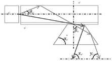
如图4所示,LED发出的可见光经入光面进入到导光板8后进行全反射的传播,并在取光凸起5处,光线被折射出导光板8,可将光进入导光板8与水平方向的夹角为θ,若导光板8的材料采用聚碳酸酯(Polycarbonate;PC)其折射率为1.58,那么可将光与水平夹角θ的最大值为arcsin(1/1.58)=±39.3°。相应的,可见光进入取光凸起5 后,其与竖直方向夹角β的范围为:50.7°~90°,与水平方向的夹角范围为0°~39.3°。As shown in FIG. 4 , the visible light emitted by the LED enters the
假如,锥台较大的底面与侧面的夹角为α,则可见光被锥台的侧面反射后与水平方向的夹角表示为:If the angle between the larger bottom surface of the frustum and the side is α, then the angle between the visible light reflected by the side of the frustum and the horizontal direction is expressed as:
y=2α-39.3°y=2α-39.3°
x=180°-2αx=180°-2α
为了使经取光凸起5出射的可见光位于竖直方向上,那么x=y,由此计算得到:α≈54.8°。此时,取光凸起5的出光方向位于竖直方向上,也即相对于水平线为90°,为了使其出光偏离角度在30°以内,也即相对于水平线出光角度在60°-120°范围内,则取39.8°≤α≤74.8°。In order to make the visible light emitted by the
作为其中一种可实现方式,自入光面,沿可见光在导光板8内的传播方向,图1中从左向右的方向,取光凸起5的设置密度依次增大。As one of the possible implementations, from the light incident surface, along the propagation direction of visible light in the
本文中的入光面位于图1中背光板的左侧面上,背光板的左侧面可以整体作为入光面,也可以部分作为入光面。The light incident surface in this paper is located on the left side of the backlight panel in FIG. 1 , and the left side of the backlight panel may be used as the light incident surface as a whole, or may be partially used as the light incident surface.
靠近入光面的取光凸起5设置的稀疏,取光凸起5之间的间隙较大,远离入光面的取光凸起5设置的相对稠密,取光凸起5之间的间隙较小。The
作为其中一种可实现方式,在液晶显示模组显示面的投影上,指纹识别模组靠近入光面。As one of the possible implementations, on the projection of the display surface of the liquid crystal display module, the fingerprint identification module is close to the light incident surface.
由于靠近入光面处取光凸起5设置的稀疏,取光凸起5之间的间隙较大,将指纹识别模组设置在此区域,此处空隙A所占的面积较大,非可见光经过空隙传播可以提高指纹识别的准确度及清晰度。Due to the sparse arrangement of the light-extracting
作为其中一种可实现方式,非可见光传感器12朝向反射膜1的一侧设置有凸透镜15。一般地,非可见光传感器12的面积比较小,而为了保证指纹识别的顺利进行,就需要足够面积的反射光进入到非可见光传感器12,通过设置凸透镜15,可以将较大面积范围内的光线汇聚到非可见光传感器12上,以供其进行指纹识别。As one of the possible implementations, a
上述的指纹识别模组例如但不限于采用如下的结构,其包括支架 10,在支架10的顶部设置用于发射非可见光的LED11,支架10内自下而上依次设置晶片粘结薄膜14(DieAttach Film;DAF)、板对板连接器13(Board To Board Connectors;BTB)、非可见光传感器12 及凸透镜15。The above-mentioned fingerprint recognition module, for example but not limited to, adopts the following structure, which includes a
作为其中一种可实现方式,所述反射膜1用于透射波长为 800nm~1200nm非可见光(红外光),用于反射波长为380nm~780nm 的可见光。As one of the possible implementations, the reflective film 1 is used for transmitting invisible light (infrared light) with a wavelength of 800 nm to 1200 nm, and for reflecting visible light with a wavelength of 380 nm to 780 nm.
第二方面,本发明提供一种显示装置,包括上述的显示面板。In a second aspect, the present invention provides a display device including the above-mentioned display panel.
显示装置例如但不限于为智能手机、平板电脑等。The display device is, for example, but not limited to, a smart phone, a tablet computer, and the like.
需要理解的是,上文如有涉及术语“中心”、“纵向”、“横向”、“上”、“下”、“前”、“后”、“左”、“右”、“竖直”、“水平”、“顶”、“底”、“内”、“外”等指示的方位或位置关系为基于附图所示的方位或位置关系,仅是为了便于描述本发明和简化描述,而不是指示或暗示所指的装置或元件必须具有特定的方位、以特定的方位构造和操作,因此不能理解为对本发明的限制。此外,术语“第一”、“第二”仅用于描述目的,而不能理解为指示或暗示相对重要性或者隐含指明所指示的技术特征的数量。由此,限定有“第一”、“第二”的特征可以明示或者隐含地包括一个或者更多个该特征。在本发明的描述中,除非另有说明,“多个”的含义是两个或两个以上。It should be understood that the terms "center", "portrait", "horizontal", "top", "bottom", "front", "rear", "left", "right", "vertical" "," "horizontal", "top", "bottom", "inside", "outside", etc. indicate the orientation or positional relationship based on the orientation or positional relationship shown in the accompanying drawings, which are only for the convenience of describing the present invention and simplifying the description , rather than indicating or implying that the indicated device or element must have a particular orientation, be constructed and operate in a particular orientation, and therefore should not be construed as limiting the invention. In addition, the terms "first" and "second" are only used for descriptive purposes, and should not be construed as indicating or implying relative importance or implying the number of indicated technical features. Thus, a feature defined as "first" or "second" may expressly or implicitly include one or more of that feature. In the description of the present invention, unless otherwise specified, "plurality" means two or more.
以上描述仅为本申请的较佳实施例以及对所运用技术原理的说明。本领域技术人员应当理解,本申请中所涉及的发明范围,并不限于上述技术特征的特定组合而成的技术方案,同时也应涵盖在不脱离发明构思的情况下,由上述技术特征或其等同特征进行任意组合而形成的其它技术方案。例如上述特征与本申请中公开的(但不限于)具有类似功能的技术特征进行互相替换而形成的技术方案。The above description is only a preferred embodiment of the present application and an illustration of the applied technical principles. Those skilled in the art should understand that the scope of the invention involved in this application is not limited to the technical solution formed by the specific combination of the above-mentioned technical features, and should also cover, without departing from the inventive concept, the above-mentioned technical features or their Other technical solutions formed by any combination of equivalent features. For example, a technical solution is formed by replacing the above-mentioned features with the technical features disclosed in this application (but not limited to) with similar functions.
Claims (7)
Priority Applications (3)
| Application Number | Priority Date | Filing Date | Title |
|---|---|---|---|
| CN202010131445.9ACN111258099B (en) | 2020-02-28 | 2020-02-28 | Display panel and display device |
| PCT/CN2021/073714WO2021169703A1 (en) | 2020-02-28 | 2021-01-26 | Display panel and display device |
| US17/424,423US11899302B2 (en) | 2020-02-28 | 2021-01-26 | Display panel and display device |
Applications Claiming Priority (1)
| Application Number | Priority Date | Filing Date | Title |
|---|---|---|---|
| CN202010131445.9ACN111258099B (en) | 2020-02-28 | 2020-02-28 | Display panel and display device |
Publications (2)
| Publication Number | Publication Date |
|---|---|
| CN111258099A CN111258099A (en) | 2020-06-09 |
| CN111258099Btrue CN111258099B (en) | 2022-07-26 |
Family
ID=70949571
Family Applications (1)
| Application Number | Title | Priority Date | Filing Date |
|---|---|---|---|
| CN202010131445.9AActiveCN111258099B (en) | 2020-02-28 | 2020-02-28 | Display panel and display device |
Country Status (3)
| Country | Link |
|---|---|
| US (1) | US11899302B2 (en) |
| CN (1) | CN111258099B (en) |
| WO (1) | WO2021169703A1 (en) |
Families Citing this family (2)
| Publication number | Priority date | Publication date | Assignee | Title |
|---|---|---|---|---|
| CN111258099B (en) | 2020-02-28 | 2022-07-26 | 京东方科技集团股份有限公司 | Display panel and display device |
| CN114764988A (en)* | 2021-01-11 | 2022-07-19 | 群创光电股份有限公司 | Backlight module and display device using same |
Citations (5)
| Publication number | Priority date | Publication date | Assignee | Title |
|---|---|---|---|---|
| JPH11326953A (en)* | 1998-05-16 | 1999-11-26 | Semiconductor Energy Lab Co Ltd | Liquid crystal display device and its production |
| CN109031512A (en)* | 2018-09-04 | 2018-12-18 | 京东方科技集团股份有限公司 | Light guide film module, front located light source and reflective display |
| CN110187537A (en)* | 2019-05-09 | 2019-08-30 | 维沃移动通信有限公司 | a terminal |
| CN110458150A (en)* | 2019-07-29 | 2019-11-15 | 深圳阜时科技有限公司 | Sensing device and electronic equipment under a kind of screen |
| CN209728221U (en)* | 2019-03-11 | 2019-12-03 | 深圳阜时科技有限公司 | A kind of backlight module, display device and electronic equipment |
Family Cites Families (8)
| Publication number | Priority date | Publication date | Assignee | Title |
|---|---|---|---|---|
| US6839108B1 (en) | 1998-05-16 | 2005-01-04 | Semiconductor Energy Laboratory Co., Ltd. | Liquid crystal display device and method of manufacturing the same |
| TWI386728B (en)* | 2009-01-20 | 2013-02-21 | Au Optronics Corp | Backlight module and liquid crystal display |
| US20120127084A1 (en)* | 2010-11-18 | 2012-05-24 | Microsoft Corporation | Variable light diffusion in interactive display device |
| US20170124376A1 (en)* | 2015-10-28 | 2017-05-04 | Qualcomm Incorporated | Infrared fluorescent backlight for optical touch and fingerprint |
| KR102648211B1 (en) | 2017-03-06 | 2024-03-14 | 쓰리엠 이노베이티브 프로퍼티즈 컴파니 | High contrast optical film and device comprising same |
| US11156757B2 (en) | 2017-03-06 | 2021-10-26 | 3M Innovative Properties Company | High contrast optical film and devices including the same |
| KR102504527B1 (en)* | 2018-03-22 | 2023-02-28 | 삼성디스플레이 주식회사 | Display device |
| CN111258099B (en) | 2020-02-28 | 2022-07-26 | 京东方科技集团股份有限公司 | Display panel and display device |
- 2020
- 2020-02-28CNCN202010131445.9Apatent/CN111258099B/enactiveActive
- 2021
- 2021-01-26USUS17/424,423patent/US11899302B2/enactiveActive
- 2021-01-26WOPCT/CN2021/073714patent/WO2021169703A1/ennot_activeCeased
Patent Citations (5)
| Publication number | Priority date | Publication date | Assignee | Title |
|---|---|---|---|---|
| JPH11326953A (en)* | 1998-05-16 | 1999-11-26 | Semiconductor Energy Lab Co Ltd | Liquid crystal display device and its production |
| CN109031512A (en)* | 2018-09-04 | 2018-12-18 | 京东方科技集团股份有限公司 | Light guide film module, front located light source and reflective display |
| CN209728221U (en)* | 2019-03-11 | 2019-12-03 | 深圳阜时科技有限公司 | A kind of backlight module, display device and electronic equipment |
| CN110187537A (en)* | 2019-05-09 | 2019-08-30 | 维沃移动通信有限公司 | a terminal |
| CN110458150A (en)* | 2019-07-29 | 2019-11-15 | 深圳阜时科技有限公司 | Sensing device and electronic equipment under a kind of screen |
Also Published As
| Publication number | Publication date |
|---|---|
| US11899302B2 (en) | 2024-02-13 |
| WO2021169703A1 (en) | 2021-09-02 |
| CN111258099A (en) | 2020-06-09 |
| US20220308382A1 (en) | 2022-09-29 |
Similar Documents
| Publication | Publication Date | Title |
|---|---|---|
| CN209625238U (en) | Under-screen optical fingerprint identification system and electronic device | |
| CN111033518B (en) | LCD fingerprint identification system, off-screen optical fingerprint identification device and electronic device | |
| EP3396588B1 (en) | Display screen, display device and mobile terminal | |
| WO2020181495A1 (en) | Back optical fingerprint recognition system and electronic device | |
| CN110286514B (en) | Display panel and display device | |
| CN210155472U (en) | Backlight Modules, Displays and Electronic Devices | |
| US20060132453A1 (en) | Frontlit illuminated touch panel | |
| CN107168465A (en) | Display module and display device | |
| CN109633959A (en) | Display device capable of in-screen fingerprint recognition | |
| CN110785771B (en) | Under-screen optical fingerprint recognition system, fingerprint recognition display device and electronic equipment | |
| WO2020192413A1 (en) | Display substrate, display module and driving method thereof, and display device | |
| CN111258099B (en) | Display panel and display device | |
| CN111586267A (en) | Optical sensing devices and electronic equipment | |
| CN212163466U (en) | Optical sensing devices and electronic equipment | |
| CN212163464U (en) | Optical sensing devices and electronic equipment | |
| CN117590648A (en) | Light emitting structure and display panel | |
| CN111464727A (en) | Optical sensing device and electronic apparatus | |
| TWM601851U (en) | Display device | |
| CN110062908A (en) | Biometric detection module and backlight module and electronic device | |
| US11307459B2 (en) | Display device comprising a switchable diffuser and a backlight module having a first region and a second region, and a mobile device comprising the same | |
| CN210573817U (en) | Biometric detection module and backlight module and electronic device | |
| CN109902653A (en) | Biological characteristic detects mould group and backlight module and electronic device | |
| CN209962256U (en) | Biometric detection modules and backlight modules, displays and electronic devices | |
| CN210155679U (en) | Biological characteristic detection module, backlight module and electronic device | |
| CN111464726A (en) | Optical sensing devices and electronic equipment |
Legal Events
| Date | Code | Title | Description |
|---|---|---|---|
| PB01 | Publication | ||
| PB01 | Publication | ||
| SE01 | Entry into force of request for substantive examination | ||
| SE01 | Entry into force of request for substantive examination | ||
| GR01 | Patent grant | ||
| GR01 | Patent grant |