CN111245400A - Bulk Acoustic Resonators, Filters, and Electronic Devices with Bridge Insertion Structures - Google Patents
Bulk Acoustic Resonators, Filters, and Electronic Devices with Bridge Insertion StructuresDownload PDFInfo
- Publication number
- CN111245400A CN111245400ACN201911226741.0ACN201911226741ACN111245400ACN 111245400 ACN111245400 ACN 111245400ACN 201911226741 ACN201911226741 ACN 201911226741ACN 111245400 ACN111245400 ACN 111245400A
- Authority
- CN
- China
- Prior art keywords
- layer
- resonator
- insertion layer
- piezoelectric
- piezoelectric layer
- Prior art date
- Legal status (The legal status is an assumption and is not a legal conclusion. Google has not performed a legal analysis and makes no representation as to the accuracy of the status listed.)
- Granted
Links
Images


Classifications
- H—ELECTRICITY
- H03—ELECTRONIC CIRCUITRY
- H03H—IMPEDANCE NETWORKS, e.g. RESONANT CIRCUITS; RESONATORS
- H03H9/00—Networks comprising electromechanical or electro-acoustic elements; Electromechanical resonators
- H03H9/02—Details
- H03H9/02007—Details of bulk acoustic wave devices
- H03H9/02015—Characteristics of piezoelectric layers, e.g. cutting angles
- H—ELECTRICITY
- H03—ELECTRONIC CIRCUITRY
- H03H—IMPEDANCE NETWORKS, e.g. RESONANT CIRCUITS; RESONATORS
- H03H9/00—Networks comprising electromechanical or electro-acoustic elements; Electromechanical resonators
- H03H9/02—Details
- H03H9/02007—Details of bulk acoustic wave devices
- H03H9/02086—Means for compensation or elimination of undesirable effects
- H—ELECTRICITY
- H03—ELECTRONIC CIRCUITRY
- H03H—IMPEDANCE NETWORKS, e.g. RESONANT CIRCUITS; RESONATORS
- H03H9/00—Networks comprising electromechanical or electro-acoustic elements; Electromechanical resonators
- H03H9/46—Filters
- H03H9/54—Filters comprising resonators of piezoelectric or electrostrictive material
Landscapes
- Physics & Mathematics (AREA)
- Acoustics & Sound (AREA)
- Piezo-Electric Or Mechanical Vibrators, Or Delay Or Filter Circuits (AREA)
Abstract
Translated fromChinese
Description
Translated fromChinese技术领域technical field
本发明的实施例涉及半导体领域,尤其涉及一种体声波谐振器,一种滤波器,一种具有上述部件中的一种的电子设备。Embodiments of the present invention relate to the field of semiconductors, and in particular, to a bulk acoustic wave resonator, a filter, and an electronic device having one of the above components.
背景技术Background technique
体声波滤波器具有低插入损耗、高矩形系数、高功率容量等优点,因此,被广泛应用在当代无线通讯系统中,是决定射频信号进出通讯系统质量的重要元器件。体声波滤波器的性能由构成它的体声波谐振器决定,如:体声波谐振器的谐振频率决定了滤波器的工作频率,有效机电耦合系数决定了滤波器的带宽,品质因数决定滤波器插入损耗。当滤波器结构一定时,其品质因数,特别是在串联谐振频率和并联谐振频率处的品质因数(或串并联阻抗),会显著影响通带插入损耗。因此,如何提高谐振器的品质因数是高性能滤波器设计的一个重要问题。体声波谐振器串联谐振频率处的品质因数(Qs)或串联阻抗(Rs) 通常由电极损耗及材料损耗决定,而体声波谐振器并联谐振频率处的品质因数 (Qp)或并联阻抗(Rp)通常受边界声波泄露影响。因此,当谐振器材料、及层叠结构确定时,Qs(或Rs)的提升空间有限,但可以通过改变谐振器的边界结构来有效改善声波的边界泄露情况,从而显著提高谐振器的Qp(或Rp)。BAW filter has the advantages of low insertion loss, high square coefficient, high power capacity, etc. Therefore, it is widely used in contemporary wireless communication systems and is an important component that determines the quality of RF signals entering and leaving the communication system. The performance of the BAW filter is determined by the BAW resonator that constitutes it. For example, the resonant frequency of the BAW resonator determines the operating frequency of the filter, the effective electromechanical coupling coefficient determines the bandwidth of the filter, and the quality factor determines the filter insertion. loss. When the filter structure is fixed, its quality factor, especially the quality factor (or series-parallel impedance) at the series resonant frequency and parallel resonant frequency, will significantly affect the passband insertion loss. Therefore, how to improve the quality factor of the resonator is an important issue in the design of high-performance filters. The quality factor (Qs) or series impedance (Rs) of a BAW resonator at the series resonant frequency is usually determined by electrode losses and material losses, while the quality factor (Qp) or parallel impedance (Rp) of a BAW resonator at the parallel resonant frequency Usually affected by boundary acoustic leakage. Therefore, when the resonator material and laminated structure are determined, the improvement space of Qs (or Rs) is limited, but the boundary leakage of acoustic waves can be effectively improved by changing the boundary structure of the resonator, thereby significantly improving the Qp (or Rs) of the resonator. Rp).
传统的薄膜体声波谐振器剖面结构示意图如图12所示,其中:100为基底, 110为声学镜,120为底电极,130为压电层,140为顶电极,15为环形凸起结 构,16为翼结构,h1为空隙的高度,h2为凸起结构15的厚度,17为桥结构。 d11-d14为各种尺寸。The cross-sectional structure diagram of the traditional thin-film bulk acoustic wave resonator is shown in Figure 12, wherein: 100 is the base, 110 is the acoustic mirror, 120 is the bottom electrode, 130 is the piezoelectric layer, 140 is the top electrode, and 15 is the annular convex structure, 16 is the wing structure, h1 is the height of the void, h2 is the thickness of the raised
在图12中,复合结构位于谐振器的上表面的有效区域边缘,使得有效区域 边缘两侧的声阻抗不匹配,限制了横向兰姆波的传输,增强了对兰姆波的反射 和转换能力,使得Rp得到一定程度的提高。在顶电极与底电极的连接侧,压电 层因底电极边缘粗糙质量较差,复合结构能使得这部分质量较差的压电层所引 起的谐振激励较小的贡献到整个电路中,能一定程度上改善
然而,以上结构对谐振器有效区域边缘的能量泄露问题改善有限,因此在改善Rp的程度上也是有限的。However, the above structure has limited improvement on the energy leakage problem at the edge of the effective area of the resonator, so the extent of improving Rp is also limited.
发明内容SUMMARY OF THE INVENTION
为进一步提高体声波谐振器的Rp值或Qp值,提出本发明。The present invention is proposed to further improve the Rp value or the Qp value of the bulk acoustic wave resonator.
根据本发明的实施例的一个方面,提出了一种体声波谐振器,其例如在谐振器顶电极与底电极的连接边区域,将部分压电层刻蚀掉,形成一种空气(介质)插入结构,此插入结构可有效提高谐振器的Rp值。相应的,该体声波谐振器包括:According to an aspect of the embodiments of the present invention, a bulk acoustic wave resonator is proposed, which, for example, in the connecting edge region between the top electrode and the bottom electrode of the resonator, a part of the piezoelectric layer is etched away to form an air (medium) The insertion structure can effectively improve the Rp value of the resonator. Correspondingly, the bulk acoustic wave resonator includes:
基底;base;
声学镜;acoustic mirror;
底电极;bottom electrode;
顶电极,与电极连接部相连,所述电极连接部形成桥部;a top electrode, connected with an electrode connection part, and the electrode connection part forms a bridge part;
压电层,piezoelectric layer,
其中:in:
声学镜、底电极、压电层、顶电极在基底的厚度方向重叠的区域为谐振器的有效区域;The area where the acoustic mirror, the bottom electrode, the piezoelectric layer, and the top electrode overlap in the thickness direction of the substrate is the effective area of the resonator;
所述谐振器还包括桥部插入结构,所述桥部插入结构包括第一插入层和第二插入层,所述第一插入层和所述第二插入层材料彼此不同且在谐振器的俯视图中至少部分重叠;The resonator also includes a bridge insertion structure including a first insertion layer and a second insertion layer, the first insertion layer and the second insertion layer being of different materials from each other and in a top view of the resonator at least partially overlap;
所述第一插入层的内端位于压电层的中间部位,所述第二插入层设置于所述第一插入层的上方,且所述第二插入层的内端与所述压电层的位于第一插入层上方的部分的第一端面相接。The inner end of the first insertion layer is located in the middle of the piezoelectric layer, the second insertion layer is arranged above the first insertion layer, and the inner end of the second insertion layer is connected to the piezoelectric layer The first end faces of the portion of the above the first interposer are connected.
可选的,所述电极连接部的下侧的至少一部分构成所述第二插入层的上侧的边界。Optionally, at least a part of the lower side of the electrode connection portion constitutes a boundary of the upper side of the second insertion layer.
可选的,在谐振器的俯视图中,第二插入层的内端落在声学镜内,或者第一插入层和第二插入层的重叠部分至少有一部分位于有效区域内。Optionally, in the top view of the resonator, the inner end of the second insertion layer falls within the acoustic mirror, or at least a part of the overlapping portion of the first insertion layer and the second insertion layer is located in the effective area.
可选的,在谐振器的俯视图中,所述第一插入层的外端处于所述底电极的端部的外侧。Optionally, in a top view of the resonator, the outer end of the first insertion layer is located outside the end of the bottom electrode.
可选的,所述底电极在所述电极连接部所在的一侧设置有平坦层,所述压电层以平层的方式覆盖所述底电极以及所述平坦层;且所述第一插入层为平层结构。Optionally, the bottom electrode is provided with a flat layer on the side where the electrode connecting portion is located, and the piezoelectric layer covers the bottom electrode and the flat layer in a flat layer manner; and the first insertion The layer is a flat layer structure.
可选的,在谐振器的俯视图中,所述第一插入层的外端在径向方向上比第二插入层的外端更远离有效区域的中心。进一步可选的,所述第一插入层的外端与所述电极连接部连接从而在谐振器的厚度方向上位于压电层与所述电极连接部之间。Optionally, in the top view of the resonator, the outer end of the first insertion layer is further away from the center of the effective area in the radial direction than the outer end of the second insertion layer. Further optionally, the outer end of the first insertion layer is connected to the electrode connection part so as to be located between the piezoelectric layer and the electrode connection part in the thickness direction of the resonator.
可选的,在谐振器的俯视图中,所述第二插入层的外端在径向方向上比第一插入层的外端更远离有效区域的中心。Optionally, in the top view of the resonator, the outer end of the second insertion layer is further away from the center of the effective area in the radial direction than the outer end of the first insertion layer.
可选的,在谐振器的俯视图中,所述第一插入层的外端与所述底电极的端部在径向方向上的距离在0-20μm的范围内。Optionally, in the top view of the resonator, the distance between the outer end of the first insertion layer and the end of the bottom electrode in the radial direction is in the range of 0-20 μm.
可选的,所述第一插入层与所述第二插入层在谐振器的厚度方向上至少部分彼此相接设置。Optionally, the first insertion layer and the second insertion layer are disposed at least partially in contact with each other in the thickness direction of the resonator.
可选的,在谐振器的厚度方向上,所述第一插入层与所述第二插入层之间至少一部分设置有一层压电层材料。Optionally, in the thickness direction of the resonator, at least a part of the first insertion layer and the second insertion layer is provided with a layer of piezoelectric layer material.
可选的,基于所述第一插入层的内端设置在压电层的中间部位,所述压电层的位于第一插入层之上的在谐振器的俯视图中与所述第一插入层的内端重叠的部分形成压电层台阶,且基于所述压电层台阶所述顶电极的端部形成顶电极台阶。进一步可选的,所述压电层台阶的端部的上侧与所述电极连接部的顶侧之间存在空隙。Optionally, based on the fact that the inner end of the first insertion layer is disposed in the middle part of the piezoelectric layer, the part of the piezoelectric layer above the first insertion layer is connected to the first insertion layer in the top view of the resonator. The overlapping portion of the inner ends of the piezoelectric layer forms a piezoelectric layer step, and an end portion of the top electrode forms a top electrode step based on the piezoelectric layer step. Further optionally, there is a gap between the upper side of the end portion of the piezoelectric layer step and the top side of the electrode connecting portion.
可选的,所述第一插入层的内端与第二插入层的内端在径向方向上的距离在0-10μm的范围内。进一步可选的,所述第一插入层的内端与声学镜的对应边缘在径向方向上的距离在0-20μm的范围内。Optionally, the distance in the radial direction between the inner end of the first insertion layer and the inner end of the second insertion layer is in the range of 0-10 μm. Further optionally, the distance between the inner end of the first insertion layer and the corresponding edge of the acoustic mirror in the radial direction is in the range of 0-20 μm.
可选的,所述第一插入层的厚度在
可选的,所述第一端面为在谐振器的俯视图中上端比下端更靠近有效区域的中心的斜面。进一步可选的,所述斜面与所述第一端面的下端所在的平面的夹角在20-90度的范围内。Optionally, the first end surface is an inclined surface whose upper end is closer to the center of the effective area than the lower end in a plan view of the resonator. Further optionally, the included angle between the inclined plane and the plane where the lower end of the first end face is located is in the range of 20-90 degrees.
可选的,所述电极连接部具有凸起结构。Optionally, the electrode connecting portion has a protruding structure.
可选的,所述电极连接部具有下凹结构。Optionally, the electrode connecting portion has a concave structure.
可选的,所述压电层具有压电第一层和压电第二层,所述压电第一层和压电第二层为不同的压电材料或者具有不同的掺杂浓度;且所述第一插入层的内端在谐振器的厚度方向上设置在压电第一层与压电第二层之间。进一步可选的,所述压电第一层为氮化铝,所述压电第二层为掺杂氮化铝。Optionally, the piezoelectric layer has a piezoelectric first layer and a piezoelectric second layer, and the piezoelectric first layer and the piezoelectric second layer are different piezoelectric materials or have different doping concentrations; and The inner end of the first insertion layer is disposed between the piezoelectric first layer and the piezoelectric second layer in the thickness direction of the resonator. Further optionally, the piezoelectric first layer is aluminum nitride, and the piezoelectric second layer is doped aluminum nitride.
可选的,所述第一插入层为介质材料或金属,所述第二插入层为空气或者不同于第一插入层的材料的介质材料或者与所述压电层的掺杂浓度不同的压电层材料。Optionally, the first insertion layer is a dielectric material or a metal, and the second insertion layer is air or a dielectric material different from the material of the first insertion layer or a voltage with a doping concentration different from that of the piezoelectric layer. Electrical layer material.
可选的,所述介质材料为以下材料中的一种或多种:二氧化硅、氮化硅、碳化硅、氮化铝、氧化铝、多孔硅、氟化非晶碳、氟聚合物、聚对二甲苯、聚芳醚、氢倍半硅氧烷、交联聚苯聚合物、双苯环丁烯、氟化二氧化硅、碳掺杂氧化物和金刚石。Optionally, the dielectric material is one or more of the following materials: silicon dioxide, silicon nitride, silicon carbide, aluminum nitride, aluminum oxide, porous silicon, fluorinated amorphous carbon, fluoropolymer, Parylenes, polyarylene ethers, hydrogen silsesquioxanes, cross-linked polyphenylene polymers, bisphenylcyclobutene, fluorinated silica, carbon-doped oxides, and diamond.
可选的,所述第一插入层的内端在压电层的厚度方向上位于所述压电层的厚度的1/3至2/3之间。Optionally, the inner end of the first insertion layer is located between 1/3 and 2/3 of the thickness of the piezoelectric layer in the thickness direction of the piezoelectric layer.
根据本发明的实施例的再一方面,提出了一种滤波器,包括上述的谐振器。According to yet another aspect of the embodiments of the present invention, a filter is proposed, including the above-mentioned resonator.
根据本发明的实施例的还一方面,提出了一种电子设备,包括上述的谐振器,或者上述的滤波器。According to yet another aspect of the embodiments of the present invention, an electronic device is provided, including the above-mentioned resonator, or the above-mentioned filter.
附图说明Description of drawings
以下描述与附图可以更好地帮助理解本发明所公布的各种实施例中的这些和其他特点、优点,图中相同的附图标记始终表示相同的部件,其中:These and other features and advantages of the various disclosed embodiments of the present invention may be better understood by the following description and accompanying drawings, in which like reference numerals refer to like parts throughout, wherein:
图1为根据本发明的一个示例性实施例的体声波谐振器的示意性俯视图;FIG. 1 is a schematic top view of a bulk acoustic wave resonator according to an exemplary embodiment of the present invention;
图2为根据本发明的一个示例性实施例的沿图1中的O-I线截得的示意性局部剖视图;2 is a schematic partial cross-sectional view taken along line O-I in FIG. 1 according to an exemplary embodiment of the present invention;
图3为根据本发明的一个示例性实施例的沿图1中的O-I线截得的示意性局部剖视图;3 is a schematic partial cross-sectional view taken along line O-I in FIG. 1 according to an exemplary embodiment of the present invention;
图4为根据本发明的一个示例性实施例的沿图1中的O-I线截得的示意性局部剖视图;4 is a schematic partial cross-sectional view taken along line O-I in FIG. 1 according to an exemplary embodiment of the present invention;
图5为根据本发明的一个示例性实施例的沿图1中的O-I线截得的示意性局部剖视图;5 is a schematic partial cross-sectional view taken along line O-I in FIG. 1 according to an exemplary embodiment of the present invention;
图6为根据本发明的一个示例性实施例的沿图1中的O-I线截得的示意性局部剖视图;6 is a schematic partial cross-sectional view taken along line O-I in FIG. 1 according to an exemplary embodiment of the present invention;
图7为根据本发明的一个示例性实施例的沿图1中的O-I线截得的示意性局部剖视图;7 is a schematic partial cross-sectional view taken along line O-I in FIG. 1 according to an exemplary embodiment of the present invention;
图8为根据本发明的一个示例性实施例的沿图1中的O-I线截得的示意性局部剖视图;8 is a schematic partial cross-sectional view taken along line O-I in FIG. 1 according to an exemplary embodiment of the present invention;
图9为根据本发明的一个示例性实施例的沿图1中的O-I线截得的示意性局部剖视图;9 is a schematic partial cross-sectional view taken along line O-I in FIG. 1 according to an exemplary embodiment of the present invention;
图10为根据本发明的一个示例性实施例的沿图1中的O-I线截得的示意性局部剖视图;10 is a schematic partial cross-sectional view taken along line O-I in FIG. 1 according to an exemplary embodiment of the present invention;
图11为根据本发明的一个示例性实施例的沿图1中的O-I线截得的示意性局部剖视图;11 is a schematic partial cross-sectional view taken along line O-I in FIG. 1 according to an exemplary embodiment of the present invention;
图12为现有技术中的体声波谐振器的示意性剖视图。FIG. 12 is a schematic cross-sectional view of a bulk acoustic wave resonator in the prior art.
具体实施方式Detailed ways
下面通过实施例,并结合附图,对本发明的技术方案作进一步具体的说明。在说明书中,相同或相似的附图标号指示相同或相似的部件。下述参照附图对本发明实施方式的说明旨在对本发明的总体发明构思进行解释,而不应当理解为对本发明的一种限制。The technical solutions of the present invention will be further described in detail below through embodiments and in conjunction with the accompanying drawings. In the specification, the same or similar reference numerals refer to the same or similar parts. The following description of the embodiments of the present invention with reference to the accompanying drawings is intended to explain the general inventive concept of the present invention, and should not be construed as a limitation of the present invention.
图1为根据本发明的一个示例性实施例的体声波谐振器的示意性俯视图,图2为根据本发明的一个示例性实施例的沿图1中的O-I线截得的示意性局部剖视图。1 is a schematic top view of a bulk acoustic wave resonator according to an exemplary embodiment of the present invention, and FIG. 2 is a schematic partial cross-sectional view taken along line O-I in FIG. 1 according to an exemplary embodiment of the present invention.
如图1所示,体声波谐振器包括底电极、压电层、顶电极,字母O代表谐振器的中心。As shown in Figure 1, the BAW resonator includes a bottom electrode, a piezoelectric layer, and a top electrode, and the letter O represents the center of the resonator.
下面参照图2的实施例说明谐振器的结构。在图2中:The structure of the resonator will be described below with reference to the embodiment of FIG. 2 . In Figure 2:
10:基底。用于承载并封闭声学器件,材料通常可选单晶硅,石英,砷化镓或蓝宝石等等。10: Substrate. Used to carry and seal acoustic devices, the material is usually single crystal silicon, quartz, gallium arsenide or sapphire, etc.
20:声学镜。声学镜位于基底的上表面或嵌于基底的内部,在图2中声学镜为嵌入基底中的空腔所构成,但是任何其它的声学镜结构如布拉格反射器也同样适用。20: Acoustic mirror. The acoustic mirror is located on the upper surface of the substrate or embedded in the interior of the substrate. In FIG. 2, the acoustic mirror is formed by a cavity embedded in the substrate, but any other acoustic mirror structure such as a Bragg reflector is also suitable.
30:底电极。底电极120沉积在声学镜的上表面,并覆盖声学镜。可将底电极120边缘刻蚀成斜面,并且该斜面位于声学镜的外边,此外还可以为阶梯状、垂直状或是其它相似的结构。底电极边缘与声学镜的距离为d13,d13的范围为0-10um。材料可为:金(Au)、钨(W)、钼(Mo)、铂(Pt),钌(Ru)、铱(Ir)、钛钨(TiW)、铝(Al)、钛(Ti)、锇(Os)、镁(Mg)、金(Au)、钨(W)、钼(Mo)、铂(Pt)、钌(Ru)、铱(Ir)、锗(Ge)、铜(Cu)、铝(Al)、铬(Cr)、砷掺杂金等类似金属形成。30: Bottom electrode. The
40:压电层。压电层材料可以为氮化铝(AlN)、掺杂氮化铝(doped AlN) 氧化锌(ZnO)、锆钛酸铅(PZT)、铌酸锂(LiNbO3)、石英(Quartz)、铌酸钾(KNbO3) 或钽酸锂(LiTaO3)等材料,其中掺杂AlN至少含一种稀土元素,如钪(Sc)、钇 (Y)、镁(Mg)、钛(Ti)、镧(La)、铈(Ce)、镨(Pr)、钕(Nd)、钷(Pm)、钐 (Sm)、铕(Eu)、钆(Gd)、铽(Tb)、镝(Dy)、钬(Ho)、铒(Er)、铥(Tm)、镱(Yb)、镥(Lu)等。40: Piezoelectric layer. The piezoelectric layer material can be aluminum nitride (AlN), doped aluminum nitride (doped AlN) zinc oxide (ZnO), lead zirconate titanate (PZT), lithium niobate (LiNbO3 ), quartz (Quartz), niobium Potassium oxide (KNbO3 ) or lithium tantalate (LiTaO3 ) and other materials, in which AlN doped contains at least one rare earth element, such as scandium (Sc), yttrium (Y), magnesium (Mg), titanium (Ti), lanthanum (La), Cerium (Ce), Praseodymium (Pr), Neodymium (Nd), Promethium (Pm), Samarium (Sm), Europium (Eu), Gadolinium (Gd), Terbium (Tb), Dysprosium (Dy), Holmium (Ho), erbium (Er), thulium (Tm), ytterbium (Yb), lutetium (Lu) and the like.
50:顶电极。材料同底电极30。顶电极上可覆盖钝化层。50: Top electrode. The material is the same as the
60:第一插入层。插入层60具有第一末端(在本发明中,第一末端为更靠近有效区域的中心的端部,对应于内端)和第二末端(在本发明中,第二末端为更远离有效区域的中心的端部,对应于外端),其第一末端位于有效区域内侧,第一末端插入压电层的距离为d11,d11的范围是0-10um,第一末端与声学镜的距离为d12,d12的范围为0-20um;第二末端延伸出底电极,其延伸出的距离为 d14,d14的范围为0-20um。插入层的高度为h11,h11的范围为
70:第二插入层。第二插入层可为空气或介质(如:SiO2、Si3N4、AlN、与压电层掺杂浓度不同的掺杂AlN等)。70: Second insertion layer. The second insertion layer can be air or a medium (eg, SiO2 , Si3 N4 , AlN, doped AlN with a different doping concentration from the piezoelectric layer, etc.).
基底10、声学镜20、底电极30、压电层40、顶电极50重叠的区域为谐振器的有效区域,在图2中如d15区域所示。The area where the
基于图2所示的实施例,一方面,在压电层中设置的第一插入层位于谐振器活塞模式应力最大的位置,因此所产生的阻抗不匹配具有更强的声波反射效果,另一方面,在压电层中设置的第一插入层由于可以延伸到非有效区域,因此,增强了有效区域与非有效区域的边界阻抗不匹配特性,从而将更多的声波反射回有效谐振区域,在电性能上表现为提高了Rp。将压电材料部分刻蚀,填充以空气后,将谐振器的有效区域固定在d15所示区域,也将有效区域与声学镜边缘的衬底分开,减少了此处横向兰姆波的泄露,同时减少了横向兰姆波在压电材料中的传输与泄露,极大的改善了因能量泄露导致的Rp降低。Based on the embodiment shown in FIG. 2 , on the one hand, the first insertion layer provided in the piezoelectric layer is located at the position where the stress of the resonator piston mode is the largest, so the resulting impedance mismatch has a stronger sound wave reflection effect, and the other On the one hand, since the first insertion layer disposed in the piezoelectric layer can extend to the non-effective area, it enhances the boundary impedance mismatch between the effective area and the non-effective area, so as to reflect more sound waves back to the effective resonance area, In the electrical performance, Rp is improved. The piezoelectric material is partially etched and filled with air, and the effective area of the resonator is fixed in the area indicated by d15, and the effective area is also separated from the substrate at the edge of the acoustic mirror, which reduces the leakage of the transverse Lamb wave here. At the same time, the transmission and leakage of transverse Lamb waves in piezoelectric materials are reduced, and the reduction of Rp caused by energy leakage is greatly improved.
图2的实施例中各部分的材料的选取也适用于本发明的其他实施例。The material selection of each part in the embodiment of FIG. 2 is also applicable to other embodiments of the present invention.
图3为根据本发明的一个示例性实施例100的沿图1中的O-I线截得的示意性局部剖视图。在图3中,110为基底,120为声学镜,130为底电极,140 为压电层,150为顶电极,160为第一插入层,170为第二插入层,180为设置在电极连接部的凸起结构。图3所示实施例与图1类似,不同之处在于顶电极 150在压电层140的第一末端附近,有向上的凸起结构180,此结构为回波反射增强结构,会使在此处传播的横向兰姆波进一步反射回有效区域,从而提高Rp。FIG. 3 is a schematic partial cross-sectional view taken along line O-I in FIG. 1 according to an
图4为根据本发明的一个示例性实施例200的沿图1中的O-I线截得的示意性局部剖视图。在图4中,210为基底,220为声学镜,230为底电极,240 为压电层,250为顶电极,260为第一插入层,270为第二插入层,280为设置在电极连接部的下降结构。图4所示实施例与图1类似,不同之处在于顶电极 250在压电层240的第一末端附近,有向下的下降结构280(下凹结构),此结构为回波反射增强结构,会使在此处传播的横向兰姆波进一步反射回有效区域,从而提高Rp。FIG. 4 is a schematic partial cross-sectional view taken along line O-I in FIG. 1 according to an
图5为根据本发明的一个示例性实施例300的沿图1中的O-I线截得的示意性局部剖视图。在图5中,310为基底,320为声学镜,330为底电极,340 为压电层,350为顶电极,360为第一插入层,370为第二插入层,380为压电层的第一端面。图5所示实施例与图1类似,不同之处在于压电层240第一末端在厚度方向上并非为垂直结构,而是呈倾斜结构,倾斜的角度为θ1,θ1的范围是20-90°。在图5所示的实施例中,第一端面为在谐振器的俯视图中上端比下端更靠近有效区域的中心的斜面。此结构为回波反射增强结构,会使在此处传播的横向兰姆波进一步反射回有效区域,从而提高Rp。FIG. 5 is a schematic partial cross-sectional view taken along line O-I in FIG. 1 according to an
图6为根据本发明的一个示例性实施例400的沿图1中的O-I线截得的示意性局部剖视图。在图6中,410为基底,420为声学镜,430为底电极,440 为压电层,450为顶电极,460为第一插入层,470为第二插入层。图6所示实施例与图1类似,不同之处在于第二插入层470用介质填充。介质可为:SiO2、 Si3N4、AlN、与压电层掺杂浓度不同的掺杂AlN等。FIG. 6 is a schematic partial cross-sectional view taken along line OI in FIG. 1 according to an
图7为根据本发明的一个示例性实施例500的沿图1中的O-I线截得的示意性局部剖视图。在图7中,510为基底,520为声学镜,530为底电极,540 为压电层,550为顶电极,560为第一插入层,570为第二插入层。图7所示实施例与图1类似,不同之处在于压电层540在第一末端的右侧,并未完全刻蚀到第一插入层,而是保留一部分压电材料,如图7所示,高度h51大于高度h52。如图7所示,在谐振器的厚度方向上,第一插入层560与第二插入层570之间至少一部分设置有一层压电层材料。FIG. 7 is a schematic partial cross-sectional view taken along line O-I in FIG. 1 according to an
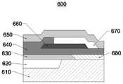
图8为根据本发明的一个示例性实施例600的沿图1中的O-I线截得的示意性局部剖视图。在图8中,610为基底,620为声学镜,630为底电极,640 为压电层,650为顶电极,660为第一插入层,670为第二插入层,680为平坦层。图8所示实施例与图1类似,不同之处在于底电极右侧填充以平坦层680。如图8所示,底电极630在电极连接部所在的一侧设置有平坦层680,压电层以平层的方式覆盖底电极以及平坦层;且第一插入层660为平层结构。虽然没有示出,平坦层也可以设置在其他实施例中。FIG. 8 is a schematic partial cross-sectional view taken along line O-I in FIG. 1 according to an
图9为根据本发明的一个示例性实施例800的沿图1中的O-I线截得的示意性局部剖视图。在图9中,810为基底,820为声学镜,830为底电极,840 为压电层,850为顶电极,860为第一插入层,870为第二插入层。图9所示实施例与图1类似,不同之处在于第一插入层继续向右延伸,直至与顶电极连接。FIG. 9 is a schematic partial cross-sectional view taken along line O-I in FIG. 1 according to an
图10为根据本发明的一个示例性实施例900的沿图1中的O-I线截得的示意性局部剖视图。在图10中,910为基底,920为声学镜,930为底电极,940 为压电层,950为顶电极,960为第一插入层,970为第二插入层,980为凸起结构。图10所示实施例与图9类似,不同之处在于顶电极950在压电层940的第一末端附近,有向上的凸起结构980,且凸起结构的第一末端981位于压电层 940第一末端的左侧。如图10所示,所述压电层台阶的端部的上侧与所述电极连接部的顶侧之间存在空隙。在图10中,第一插入层960的外端与电极连接部连接从而在谐振器的厚度方向上位于压电层940与所述电极连接部之间。相对于图9中的实施例,此结构避免了压电层第一末端因粗糙等问题对谐振器的影响,使得因此部分质量较差的压电材料引起的谐振激励在整体的电路中贡献最小,能一定程度上改善
图11为根据本发明的一个示例性实施例1000的沿图1中的O-I线截得的示意性局部剖视图。在图11中,1010为基底,1020为声学镜,1030为底电极, 1040为第一压电层,1041为第二压电层,1050为顶电极,1060为第一插入层, 1070为第二插入层。图11所示实施例与图2类似,不同之处在于压电层由两种不同的压电材料组成,或由掺杂浓度不同的压电材料组成。在图11所示的实施例中,第一压电层1040为AlN,第二压电层1041为掺杂AlN。11 is a schematic partial cross-sectional view taken along line O-I in FIG. 1 according to an
如图9-10所示,第一插入层的外端在径向方向上比第二插入层的外端更远离有效区域的中心。而在图2-8以及图11中,第二插入层的外端在径向方向上比第一插入层的外端更远离有效区域的中心。As shown in Figures 9-10, the outer end of the first interposer is radially farther from the center of the active area than the outer end of the second interposer. Whereas in FIGS. 2-8 and 11 , the outer end of the second insertion layer is farther from the center of the active area in the radial direction than the outer end of the first insertion layer.
如图2-11所示,第一插入层的外端处于底电极的端部的外侧。本发明不限于此,在俯视图中,第一插入层的外端可以与底电极的端部齐平,也可以位于底电极的端部的内侧。As shown in FIGS. 2-11 , the outer end of the first insertion layer is outside the end of the bottom electrode. The present invention is not limited thereto, and in a plan view, the outer end of the first insertion layer may be flush with the end of the bottom electrode, or may be located inside the end of the bottom electrode.
如图2-6以及8-11中,所述第一插入层与所述第二插入层在谐振器的厚度方向上至少部分彼此相接设置。As shown in FIGS. 2-6 and 8-11 , the first insertion layer and the second insertion layer are disposed at least partially in contact with each other in the thickness direction of the resonator.
如图2-11所示,基于所述第一插入层的内端设置在压电层的中间部位,所述压电层的位于第一插入层之上的在谐振器的俯视图中与所述第一插入层的内端重叠的部分形成压电层台阶,且基于所述压电层台阶所述顶电极的端部形成顶电极台阶。需要指出的是,在本发明中,中间部位表示第一插入层的内端的顶面与压电层的顶面存在距离且第一插入层的内端的底面与压电层的底面存在距离。在进一步的实施例中,第一插入层的内端在压电层的厚度方向上位于所述压电层的厚度的1/3至2/3之间。As shown in FIG. 2-11 , because the inner end of the first insertion layer is disposed in the middle of the piezoelectric layer, the portion of the piezoelectric layer above the first insertion layer is the same as the above in the top view of the resonator. A portion where the inner ends of the first insertion layer overlap forms a piezoelectric layer step, and an end portion of the top electrode forms a top electrode step based on the piezoelectric layer step. It should be pointed out that, in the present invention, the middle part means that the top surface of the inner end of the first insertion layer has a distance from the top surface of the piezoelectric layer and the bottom surface of the inner end of the first insertion layer has a distance from the bottom surface of the piezoelectric layer. In a further embodiment, the inner end of the first insertion layer is located between 1/3 and 2/3 of the thickness of the piezoelectric layer in the thickness direction of the piezoelectric layer.
在本发明中,如图2所示,第一插入层的内端与第二插入层的内端在径向方向上的距离d11在0-10μm的范围内。第一插入层的内端与声学镜的对应边缘在径向方向上的距离d12在0-20μm的范围内。第一插入层的厚度在
需要专门指出的是,在本发明中,对于数值范围,不仅可以为给出的范围端点值,而且可以为该数值范围的均值或中点值。It should be specially pointed out that, in the present invention, for a numerical range, not only the end value of the given range, but also the mean value or midpoint value of the numerical range can be used.
基于以上实施例及其附图,本发明提出了如下技术方案:Based on the above embodiments and the accompanying drawings, the present invention proposes the following technical solutions:
1、一种体声波谐振器,包括:1. A bulk acoustic wave resonator, comprising:
基底;base;
声学镜;acoustic mirror;
底电极;bottom electrode;
顶电极,与电极连接部相连,所述电极连接部形成桥部;a top electrode, connected with an electrode connection part, and the electrode connection part forms a bridge part;
压电层,piezoelectric layer,
其中:in:
声学镜、底电极、压电层、顶电极在基底的厚度方向重叠的区域为谐振器的有效区域;The area where the acoustic mirror, the bottom electrode, the piezoelectric layer, and the top electrode overlap in the thickness direction of the substrate is the effective area of the resonator;
所述谐振器还包括桥部插入结构,所述桥部插入结构包括第一插入层和第二插入层,所述第一插入层和所述第二插入层材料彼此不同且在谐振器的俯视图中至少部分重叠;The resonator also includes a bridge insertion structure including a first insertion layer and a second insertion layer, the first insertion layer and the second insertion layer being of different materials from each other and in a top view of the resonator at least partially overlap;
所述第一插入层的内端位于压电层的中间部位,所述第二插入层设置于所述第一插入层的上方,且所述第二插入层的内端与所述压电层的位于第一插入层上方的部分的第一端面相接。The inner end of the first insertion layer is located in the middle of the piezoelectric layer, the second insertion layer is arranged above the first insertion layer, and the inner end of the second insertion layer is connected to the piezoelectric layer The first end faces of the portion of the above the first interposer are connected.
需要指出的是,所述第一插入层和所述第二插入层材料彼此不同中的“材料彼此不同”不仅包括两个插入层在材料选取上的不同,例如为金属或者介质,或者介质与空气等,也包括两个插入层可以在基本物质相同的基础上存在不同的掺杂浓度,这些均在本发明的保护范围之内。It should be pointed out that the "materials are different from each other" in the materials of the first intercalation layer and the second intercalation layer are different from each other not only includes the difference in the material selection of the two intercalation layers, such as metal or medium, or the medium and the Air, etc., including the two insertion layers may have different doping concentrations on the basis of the same basic material, which are all within the protection scope of the present invention.
2、一种滤波器,包括上述的谐振器。2. A filter comprising the above resonator.
3、一种电子设备,包括上述的谐振器,或者上述的滤波器。需要指出的是,这里的电子设备,包括但不限于射频前端、滤波放大模块等中间产品,以及手机、WIFI、无人机等终端产品。3. An electronic device comprising the above-mentioned resonator, or the above-mentioned filter. It should be pointed out that the electronic equipment here includes but is not limited to intermediate products such as RF front-end, filter and amplifier modules, and terminal products such as mobile phones, WIFI, and drones.
尽管已经示出和描述了本发明的实施例,对于本领域的普通技术人员而言,可以理解在不脱离本发明的原理和精神的情况下可以对这些实施例进行变化,本发明的范围由所附权利要求及其等同物限定。Although embodiments of the present invention have been shown and described, it will be understood by those of ordinary skill in the art that changes may be made to these embodiments without departing from the principles and spirit of the invention, the scope of which is determined by It is defined by the appended claims and their equivalents.
Claims (27)

Priority Applications (1)
| Application Number | Priority Date | Filing Date | Title |
|---|---|---|---|
| CN201911226741.0ACN111245400B (en) | 2019-12-04 | 2019-12-04 | Bulk acoustic wave resonator, filter and electronic device having bridge insertion structure |
Applications Claiming Priority (1)
| Application Number | Priority Date | Filing Date | Title |
|---|---|---|---|
| CN201911226741.0ACN111245400B (en) | 2019-12-04 | 2019-12-04 | Bulk acoustic wave resonator, filter and electronic device having bridge insertion structure |
Publications (2)
| Publication Number | Publication Date |
|---|---|
| CN111245400Atrue CN111245400A (en) | 2020-06-05 |
| CN111245400B CN111245400B (en) | 2025-05-13 |
Family
ID=70868980
Family Applications (1)
| Application Number | Title | Priority Date | Filing Date |
|---|---|---|---|
| CN201911226741.0AActiveCN111245400B (en) | 2019-12-04 | 2019-12-04 | Bulk acoustic wave resonator, filter and electronic device having bridge insertion structure |
Country Status (1)
| Country | Link |
|---|---|
| CN (1) | CN111245400B (en) |
Cited By (8)
| Publication number | Priority date | Publication date | Assignee | Title |
|---|---|---|---|---|
| CN111917393A (en)* | 2020-06-22 | 2020-11-10 | 诺思(天津)微系统有限责任公司 | Bulk acoustic wave resonator and manufacturing method, bulk acoustic wave resonator assembly, filter and electronic equipment |
| CN111934640A (en)* | 2020-06-28 | 2020-11-13 | 诺思(天津)微系统有限责任公司 | Bulk acoustic wave resonators, filters and electronics with insertion layers to boost power |
| CN112165310A (en)* | 2020-09-25 | 2021-01-01 | 中国科学技术大学 | A thin film bulk acoustic wave resonator filter |
| CN114006592A (en)* | 2020-07-28 | 2022-02-01 | 三星电机株式会社 | Bulk acoustic wave resonator |
| CN114257197A (en)* | 2020-09-21 | 2022-03-29 | 中芯集成电路(宁波)有限公司上海分公司 | Film bulk acoustic resonator, manufacturing method thereof and filter |
| CN114744974A (en)* | 2021-01-07 | 2022-07-12 | 诺思(天津)微系统有限责任公司 | Bulk acoustic wave resonator and its manufacturing method, filter and electronic equipment |
| CN117013978A (en)* | 2022-12-14 | 2023-11-07 | 北京芯溪半导体科技有限公司 | Bulk acoustic wave resonator, preparation method thereof, filter and electronic equipment |
| CN117013979A (en)* | 2022-12-14 | 2023-11-07 | 北京芯溪半导体科技有限公司 | Bulk acoustic wave resonator, preparation method thereof, filter and electronic equipment |
Citations (5)
| Publication number | Priority date | Publication date | Assignee | Title |
|---|---|---|---|---|
| CN101908865A (en)* | 2010-08-20 | 2010-12-08 | 庞慰 | Bulk wave resonator and its processing method |
| US20100327697A1 (en)* | 2009-06-24 | 2010-12-30 | Avago Technologies Wireless Ip (Singapore) Pte. Ltd. | Acoustic resonator structure comprising a bridge |
| JP2015139167A (en)* | 2014-01-23 | 2015-07-30 | 太陽誘電株式会社 | Piezoelectric thin film resonator, filter and duplexer |
| JP2017225042A (en)* | 2016-06-16 | 2017-12-21 | 太陽誘電株式会社 | Piezoelectric thin film resonator, filter, and multiplexer |
| CN109802646A (en)* | 2018-12-26 | 2019-05-24 | 天津大学 | Resonator, filter with temperature compensating layer |
- 2019
- 2019-12-04CNCN201911226741.0Apatent/CN111245400B/enactiveActive
Patent Citations (5)
| Publication number | Priority date | Publication date | Assignee | Title |
|---|---|---|---|---|
| US20100327697A1 (en)* | 2009-06-24 | 2010-12-30 | Avago Technologies Wireless Ip (Singapore) Pte. Ltd. | Acoustic resonator structure comprising a bridge |
| CN101908865A (en)* | 2010-08-20 | 2010-12-08 | 庞慰 | Bulk wave resonator and its processing method |
| JP2015139167A (en)* | 2014-01-23 | 2015-07-30 | 太陽誘電株式会社 | Piezoelectric thin film resonator, filter and duplexer |
| JP2017225042A (en)* | 2016-06-16 | 2017-12-21 | 太陽誘電株式会社 | Piezoelectric thin film resonator, filter, and multiplexer |
| CN109802646A (en)* | 2018-12-26 | 2019-05-24 | 天津大学 | Resonator, filter with temperature compensating layer |
Cited By (13)
| Publication number | Priority date | Publication date | Assignee | Title |
|---|---|---|---|---|
| CN111917393A (en)* | 2020-06-22 | 2020-11-10 | 诺思(天津)微系统有限责任公司 | Bulk acoustic wave resonator and manufacturing method, bulk acoustic wave resonator assembly, filter and electronic equipment |
| CN111917393B (en)* | 2020-06-22 | 2021-06-01 | 诺思(天津)微系统有限责任公司 | Bulk acoustic wave resonator and manufacturing method, bulk acoustic wave resonator assembly, filter and electronic equipment |
| WO2022001861A1 (en)* | 2020-06-28 | 2022-01-06 | 诺思(天津)微系统有限责任公司 | Bulk acoustic resonator having insertion layer to increase power, and filter and electronic device |
| CN111934640A (en)* | 2020-06-28 | 2020-11-13 | 诺思(天津)微系统有限责任公司 | Bulk acoustic wave resonators, filters and electronics with insertion layers to boost power |
| CN111934640B (en)* | 2020-06-28 | 2021-06-01 | 诺思(天津)微系统有限责任公司 | Bulk acoustic wave resonators, filters and electronics with insertion layers to boost power |
| CN114006592A (en)* | 2020-07-28 | 2022-02-01 | 三星电机株式会社 | Bulk acoustic wave resonator |
| CN114257197A (en)* | 2020-09-21 | 2022-03-29 | 中芯集成电路(宁波)有限公司上海分公司 | Film bulk acoustic resonator, manufacturing method thereof and filter |
| CN114257197B (en)* | 2020-09-21 | 2025-03-11 | 中芯集成电路(宁波)有限公司上海分公司 | A thin film bulk acoustic wave resonator and its manufacturing method and filter |
| CN112165310A (en)* | 2020-09-25 | 2021-01-01 | 中国科学技术大学 | A thin film bulk acoustic wave resonator filter |
| CN114744974A (en)* | 2021-01-07 | 2022-07-12 | 诺思(天津)微系统有限责任公司 | Bulk acoustic wave resonator and its manufacturing method, filter and electronic equipment |
| CN117013978A (en)* | 2022-12-14 | 2023-11-07 | 北京芯溪半导体科技有限公司 | Bulk acoustic wave resonator, preparation method thereof, filter and electronic equipment |
| CN117013979A (en)* | 2022-12-14 | 2023-11-07 | 北京芯溪半导体科技有限公司 | Bulk acoustic wave resonator, preparation method thereof, filter and electronic equipment |
| CN117013979B (en)* | 2022-12-14 | 2024-06-04 | 北京芯溪半导体科技有限公司 | Bulk acoustic wave resonator, preparation method thereof, filter and electronic equipment |
Also Published As
| Publication number | Publication date |
|---|---|
| CN111245400B (en) | 2025-05-13 |
Similar Documents
| Publication | Publication Date | Title |
|---|---|---|
| CN111245400A (en) | Bulk Acoustic Resonators, Filters, and Electronic Devices with Bridge Insertion Structures | |
| CN110061712B (en) | Acoustic resonator, filter and electronic device comprising annular protrusion Liang Yan structure | |
| US10727808B2 (en) | Bulk acoustic wave resonator comprising a ring | |
| EP4027517A1 (en) | Bulk acoustic wave resonator with piezoelectric layer having insert structure, and filter and electronic device | |
| US10284173B2 (en) | Acoustic resonator device with at least one air-ring and frame | |
| EP4068628A1 (en) | Bulk acoustic resonator with electrode having void layer, and filter and electronic device | |
| US9401691B2 (en) | Acoustic resonator device with air-ring and temperature compensating layer | |
| CN101908865B (en) | Bulk wave resonator and its processing method | |
| CN111355466B (en) | Bulk acoustic resonator with multi-beam eave gap, filter and electronic device | |
| CN111193489B (en) | Bulk acoustic resonators, filters and electronic devices | |
| WO2021027319A1 (en) | Resonator having composite annular structure, filter and electronic device | |
| CN111371425B (en) | Resonator, filter and electronic equipment with top electrode connecting part provided with extension structure | |
| CN114070233A (en) | Bulk Acoustic Resonators, Filters, and Electronics for Spurious Mode Reduction | |
| WO2022228385A1 (en) | Bulk acoustic wave resonator having thickened electrode, filter, and electronic device | |
| WO2020140654A1 (en) | Apparatus and method for adjusting performance of acoustic resonator on the basis of beam and eave dimension | |
| CN114389559A (en) | Bulk acoustic wave resonator, bulk acoustic wave resonator component, filter, and electronic device | |
| CN111262547A (en) | Bulk Acoustic Resonators, MEMS Devices, Filters and Electronics | |
| WO2023016500A1 (en) | Bulk acoustic resonator having two piezoelectric layers, filter, and electronic device | |
| CN114553169A (en) | Bulk acoustic wave resonator, filter and electronic device using convex structure to reduce acoustic impedance | |
| CN117595818B (en) | Thin film bulk acoustic resonator, method of manufacturing the same, and related apparatus | |
| WO2024087628A1 (en) | Bulk acoustic wave resonator for selecting angle of protruding structure to improve performance | |
| CN111934640B (en) | Bulk acoustic wave resonators, filters and electronics with insertion layers to boost power | |
| CN111010139B (en) | Bulk acoustic resonators, filters and electronic devices | |
| WO2023030359A1 (en) | Bulk acoustic resonator comprising gap electrode, filter and electronic device | |
| CN111313857B (en) | Bulk acoustic resonator provided with insertion structure and temperature compensation layer, filter and electronic device |
Legal Events
| Date | Code | Title | Description |
|---|---|---|---|
| PB01 | Publication | ||
| PB01 | Publication | ||
| SE01 | Entry into force of request for substantive examination | ||
| SE01 | Entry into force of request for substantive examination | ||
| GR01 | Patent grant | ||
| GR01 | Patent grant |