CN111243441B - Display panel, driving method thereof and display device - Google Patents
Display panel, driving method thereof and display deviceDownload PDFInfo
- Publication number
- CN111243441B CN111243441BCN202010167914.2ACN202010167914ACN111243441BCN 111243441 BCN111243441 BCN 111243441BCN 202010167914 ACN202010167914 ACN 202010167914ACN 111243441 BCN111243441 BCN 111243441B
- Authority
- CN
- China
- Prior art keywords
- display
- data
- line
- numbered
- multiplexer
- Prior art date
- Legal status (The legal status is an assumption and is not a legal conclusion. Google has not performed a legal analysis and makes no representation as to the accuracy of the status listed.)
- Active
Links
Images


Classifications
- G—PHYSICS
- G09—EDUCATION; CRYPTOGRAPHY; DISPLAY; ADVERTISING; SEALS
- G09F—DISPLAYING; ADVERTISING; SIGNS; LABELS OR NAME-PLATES; SEALS
- G09F9/00—Indicating arrangements for variable information in which the information is built-up on a support by selection or combination of individual elements
- G09F9/30—Indicating arrangements for variable information in which the information is built-up on a support by selection or combination of individual elements in which the desired character or characters are formed by combining individual elements
- G—PHYSICS
- G09—EDUCATION; CRYPTOGRAPHY; DISPLAY; ADVERTISING; SEALS
- G09G—ARRANGEMENTS OR CIRCUITS FOR CONTROL OF INDICATING DEVICES USING STATIC MEANS TO PRESENT VARIABLE INFORMATION
- G09G3/00—Control arrangements or circuits, of interest only in connection with visual indicators other than cathode-ray tubes
- G09G3/20—Control arrangements or circuits, of interest only in connection with visual indicators other than cathode-ray tubes for presentation of an assembly of a number of characters, e.g. a page, by composing the assembly by combination of individual elements arranged in a matrix no fixed position being assigned to or needed to be assigned to the individual characters or partial characters
- G—PHYSICS
- G09—EDUCATION; CRYPTOGRAPHY; DISPLAY; ADVERTISING; SEALS
- G09G—ARRANGEMENTS OR CIRCUITS FOR CONTROL OF INDICATING DEVICES USING STATIC MEANS TO PRESENT VARIABLE INFORMATION
- G09G2300/00—Aspects of the constitution of display devices
- G09G2300/04—Structural and physical details of display devices
- G09G2300/0421—Structural details of the set of electrodes
- G09G2300/0426—Layout of electrodes and connections
- G—PHYSICS
- G09—EDUCATION; CRYPTOGRAPHY; DISPLAY; ADVERTISING; SEALS
- G09G—ARRANGEMENTS OR CIRCUITS FOR CONTROL OF INDICATING DEVICES USING STATIC MEANS TO PRESENT VARIABLE INFORMATION
- G09G2300/00—Aspects of the constitution of display devices
- G09G2300/04—Structural and physical details of display devices
- G09G2300/0421—Structural details of the set of electrodes
- G09G2300/043—Compensation electrodes or other additional electrodes in matrix displays related to distortions or compensation signals, e.g. for modifying TFT threshold voltage in column driver
- G—PHYSICS
- G09—EDUCATION; CRYPTOGRAPHY; DISPLAY; ADVERTISING; SEALS
- G09G—ARRANGEMENTS OR CIRCUITS FOR CONTROL OF INDICATING DEVICES USING STATIC MEANS TO PRESENT VARIABLE INFORMATION
- G09G2310/00—Command of the display device
- G09G2310/02—Addressing, scanning or driving the display screen or processing steps related thereto
- G09G2310/0264—Details of driving circuits
- G09G2310/0297—Special arrangements with multiplexing or demultiplexing of display data in the drivers for data electrodes, in a pre-processing circuitry delivering display data to said drivers or in the matrix panel, e.g. multiplexing plural data signals to one D/A converter or demultiplexing the D/A converter output to multiple columns
- G—PHYSICS
- G09—EDUCATION; CRYPTOGRAPHY; DISPLAY; ADVERTISING; SEALS
- G09G—ARRANGEMENTS OR CIRCUITS FOR CONTROL OF INDICATING DEVICES USING STATIC MEANS TO PRESENT VARIABLE INFORMATION
- G09G2310/00—Command of the display device
- G09G2310/06—Details of flat display driving waveforms
- G09G2310/067—Special waveforms for scanning, where no circuit details of the gate driver are given
- G—PHYSICS
- G09—EDUCATION; CRYPTOGRAPHY; DISPLAY; ADVERTISING; SEALS
- G09G—ARRANGEMENTS OR CIRCUITS FOR CONTROL OF INDICATING DEVICES USING STATIC MEANS TO PRESENT VARIABLE INFORMATION
- G09G2310/00—Command of the display device
- G09G2310/08—Details of timing specific for flat panels, other than clock recovery
- G—PHYSICS
- G09—EDUCATION; CRYPTOGRAPHY; DISPLAY; ADVERTISING; SEALS
- G09G—ARRANGEMENTS OR CIRCUITS FOR CONTROL OF INDICATING DEVICES USING STATIC MEANS TO PRESENT VARIABLE INFORMATION
- G09G2320/00—Control of display operating conditions
- G09G2320/02—Improving the quality of display appearance
- G09G2320/0252—Improving the response speed
Landscapes
- Engineering & Computer Science (AREA)
- Physics & Mathematics (AREA)
- General Physics & Mathematics (AREA)
- Theoretical Computer Science (AREA)
- Computer Hardware Design (AREA)
- Control Of Indicators Other Than Cathode Ray Tubes (AREA)
Abstract
Translated fromChinese
Description
Translated fromChinese技术领域technical field
本发明实施例涉及但不限于显示技术领域,尤指一种显示母板及其制备方法、显示基板和显示装置。The embodiments of the present invention relate to, but are not limited to, the field of display technology, and in particular, refer to a display motherboard and a method for manufacturing the same, a display substrate and a display device.
背景技术Background technique
近年来,虚拟现实(Virtual Reality,简称VR)/增强现实(Augmented Reality,简称AR)技术已逐步应用到显示、游戏、医疗等领域。虚拟现实是一种可以创建和体验虚拟世界的计算机仿真技术,计算机生成一种模拟环境,利用多源信息融合的交互式三维动态视景和实体行为的系统仿真使用户沉浸到该环境中,能够给人们带来了全新的视觉感受,越来越受到人们的关注和喜爱。此外,随着移动终端的快速发展,手机游戏已成为年轻人一项重要的娱乐休闲方式。In recent years, Virtual Reality (VR)/Augmented Reality (AR) technology has been gradually applied to display, game, medical and other fields. Virtual reality is a computer simulation technology that can create and experience virtual worlds. The computer generates a simulated environment, and uses multi-source information fusion interactive three-dimensional dynamic vision and system simulation of physical behavior to immerse users in the environment and be able to immerse users in the environment. It has brought a new visual experience to people, and it has attracted more and more people's attention and love. In addition, with the rapid development of mobile terminals, mobile games have become an important way of entertainment and leisure for young people.
为了满足人们在虚拟现实或手机游戏中的视觉享受,都需要显示面板采用较高的刷新频率。然后,当显示面板的刷新速度提高到120Hz时,传统的显示面板结构以及驱动方式存在阈值电压(Vth)补偿能力不足的问题,从而造成显示不均匀。In order to satisfy people's visual enjoyment in virtual reality or mobile games, a higher refresh rate is required for the display panel. Then, when the refresh rate of the display panel is increased to 120 Hz, the conventional display panel structure and driving method have the problem of insufficient threshold voltage (Vth) compensation capability, resulting in uneven display.
发明内容SUMMARY OF THE INVENTION
以下是对本文详细描述的主题的概述。本概述并非是为了限制权利要求的保护范围。The following is an overview of the topics detailed in this article. This summary is not intended to limit the scope of protection of the claims.
本发明实施例所要解决的技术问题是,提供一种显示面板及其驱动方法、显示装置,以解决现有技术存在的阈值电压补偿能力不足的问题。The technical problem to be solved by the embodiments of the present invention is to provide a display panel, a driving method thereof, and a display device to solve the problem of insufficient threshold voltage compensation capability in the prior art.
为了解决上述技术问题,本发明实施例提供了一种显示面板,包括由M+1条栅线和N对数据线交叉限定出呈阵列排布的M*N个显示单元,每对数据线包括第一数据线和第二数据线;In order to solve the above technical problems, an embodiment of the present invention provides a display panel, including M*N display units arranged in an array defined by the intersection of M+1 gate lines and N pairs of data lines, each pair of data lines includes a first data line and a second data line;
第m显示行中,奇数显示列的显示单元与第m条栅线连接,偶数显示列的显示单元与第m+1条栅线连接;第n显示列中,奇数显示行的显示单元与第n对数据线的第一数据线连接,偶数显示行的显示单元与第n对数据线的第二数据线连接;或者,In the mth display row, the display cells of the odd-numbered display columns are connected to the mth gate line, and the display cells of the even-numbered display columns are connected to the m+1th gate line; in the nth display column, the display cells of the odd-numbered display rows are connected to the mth gate line. The first data lines of the n pairs of data lines are connected, and the display units of the even-numbered display rows are connected to the second data lines of the nth pair of data lines; or,
第m显示行中,偶数显示列的显示单元与第m条栅线连接,奇数显示列的显示单元与第m+1条栅线连接;第n显示列中,偶数显示行的显示单元与第n对数据线的第一数据线连接,奇数显示行的显示单元与第n对数据线的第二数据线连接;In the mth display row, the display cells of the even-numbered display columns are connected to the mth gate line, and the display cells of the odd-numbered display columns are connected to the m+1th gate line; in the nth display column, the display cells of the even-numbered display rows are connected to the mth gate line. The first data lines of the n pairs of data lines are connected, and the display units of the odd-numbered display lines are connected to the second data lines of the nth pair of data lines;
其中,M和N为大于等于2的偶数,m=1,2,……,M,n=1,2,……,N。Wherein, M and N are even numbers greater than or equal to 2, m=1, 2, ..., M, n=1, 2, ..., N.
在一些可能的实现方式中,所述第m条栅线设置在所述第m显示行远离第m+1显示行的一侧,所述第n对数据线的第一数据线和第二数据线设置在所述第n显示列的两侧。In some possible implementations, the m th gate line is disposed on a side of the m th display row away from the m+1 th display row, and the first data line and the second data line of the n th pair of data lines Lines are arranged on both sides of the nth display column.
在一些可能的实现方式中,在n=2,……,N-1时,所述第n对数据线的第一数据线设置在所述第n-1显示列与第n显示列之间,所述第n对数据线的第二数据线设置在所述第n显示列与第n+1显示列之间;在n=1时,所述第一对数据线的第一数据线设置在所述第一显示列远离第二显示列的一侧;在n=N时,所述第N对数据线的第二数据线设置在所述第N显示列远离第N-1显示列的一侧。In some possible implementations, when n=2,...,N-1, the first data line of the nth pair of data lines is disposed between the n-1th display column and the nth display column , the second data line of the n-th pair of data lines is set between the n-th display column and the n+1-th display column; when n=1, the first data line of the first pair of data lines is set between the n-th display column and the n+1-th display column; On the side of the first display column far away from the second display column; when n=N, the second data line of the Nth pair of data lines is arranged on the side of the Nth display column far away from the N−1th display column side.
在一些可能的实现方式中,还包括数据控制器,所述数据控制器与所述N对数据线中的第一数据线和第二数据线连接,用于使相邻的显示列之间的第一数据线和第二数据线同时向显示单元写入显示数据。In some possible implementations, a data controller is also included, the data controller is connected to the first data line and the second data line in the N pairs of data lines, and is used for enabling the communication between adjacent display columns. The first data line and the second data line simultaneously write display data to the display unit.
在一些可能的实现方式中,所述数据控制器包括第一多路开关和第二多路开关,所述第一多路开关用于使奇数显示列的第一数据线和偶数显示列的第二数据线同时向显示单元写入显示数据;所述第二多路开关用于使奇数显示列的第二数据线和偶数显示列的第一数据线同时向显示单元写入显示数据。In some possible implementations, the data controller includes a first multiplexer and a second multiplexer, and the first multiplexer is configured to make the first data line of the odd-numbered display column and the first data line of the even-numbered display column The two data lines simultaneously write display data to the display unit; the second multiplexer is used to enable the second data lines of odd-numbered display columns and the first data lines of even-numbered display columns to simultaneously write display data to the display unit.
在一些可能的实现方式中,所述第一多路开关包括N/2个第一开关和N/2个第二开关,所述N/2个第一开关分别与奇数显示列的第一数据线连接,所述N/2个第二开关分别与偶数显示列的第二数据线连接;所述第二多路开关包括的N/2个第一开关和N/2个第二开关,所述N/2个第一开关分别与偶数显示列的第一数据线连接,N/2个第二开关分别与奇数显示列的第二数据线连接。In some possible implementations, the first multiplexer includes N/2 first switches and N/2 second switches, and the N/2 first switches are respectively associated with the first data of odd-numbered display columns. The N/2 second switches are respectively connected to the second data lines of the even-numbered display columns; the second multiplexer includes N/2 first switches and N/2 second switches, so The N/2 first switches are respectively connected to the first data lines of the even-numbered display columns, and the N/2 second switches are respectively connected to the second data lines of the odd-numbered display columns.
在一些可能的实现方式中,还包括第一控制线和第二控制线,所述第一控制线与所述第一多路开关中所有开关的控制端连接,所述第二控制线与所述第二多路开关中所有开关的控制端连接;所述第一控制线和第二控制线用于按照预设时序,导通所述第一多路开关中所有开关,关断所述第二多路开关中所有开关;或者,关断所述第一多路开关中所有开关,导通所述第二多路开关中所有开关。In some possible implementations, it further includes a first control line and a second control line, the first control line is connected to the control terminals of all switches in the first multiplexer, and the second control line is connected to all switches in the first multiplexer. the control terminals of all switches in the second multi-way switch are connected; the first control line and the second control line are used to turn on all the switches in the first multi-way switch according to the preset time sequence, and turn off the first multi-way switch. All switches in the second multiplexer; or, all switches in the first multiplexer are turned off, and all switches in the second multiplexer are turned on.
本发明实施例还提供了一种显示装置,包括前述的显示面板。Embodiments of the present invention also provide a display device, including the aforementioned display panel.
本发明实施例还提供了一种采用前述显示面板的显示面板的驱动方法,包括:在m=2,……,M时,An embodiment of the present invention further provides a method for driving a display panel using the aforementioned display panel, including: when m=2, ......, M,
向第m-1条栅线和第m条栅线输出扫描信号,向第m显示行中奇数显示列的显示单元和第m-1显示行中偶数显示列的显示单元写入显示数据;Output scanning signals to the m-1 th grid line and the m th grid line, and write display data to the display unit of the odd-numbered display column in the m-th display row and the display unit of the even-numbered display column in the m-1 display row;
向第m条栅线和第m+1条栅线输出扫描信号,向第m显示行中偶数显示列的显示单元和第m+1显示行中奇数显示列的显示单元写入显示数据。The scan signal is output to the m-th gate line and the m+1-th gate line, and display data is written to the display cells of the even-numbered display columns in the m-th display row and the display cells of the odd-numbered display columns of the m+1-th display row.
在一些可能的实现方式中,向第m-1条栅线和第m条栅线输出扫描信号,向第m显示行中奇数显示列的显示单元和第m-1显示行中偶数显示列的显示单元写入显示数据,包括:In some possible implementations, the scan signal is output to the m-1 th gate line and the m th gate line, and to the display units of the odd-numbered display columns in the m-th display row and to the display units of the even-numbered display columns in the m-1 th display row The display unit writes display data, including:
向第m-1条栅线和第m条栅线输出扫描信号,第一控制线向第一多路开关输出导通信号,第二控制线向第二多路开关输出关断信号,与所述第一多路开关连接的第一数据线向第m显示行中奇数显示列的显示单元写入显示数据,与所述第一多路开关连接的第二数据线向第m-1显示行中偶数显示列的显示单元写入显示数据。The scan signal is output to the m-1th gate line and the mth gate line, the first control line outputs a turn-on signal to the first multiplexer, and the second control line outputs a turn-off signal to the second multiplexer, which is consistent with all The first data line connected to the first multiplexer writes display data to the display units of the odd-numbered display columns in the mth display row, and the second data line connected to the first multiplexer writes display data to the m-1th display row Display data is written to the display cells of the even-numbered display column.
在一些可能的实现方式中,向第m条栅线和第m+1条栅线输出扫描信号,向第m显示行中偶数显示列的显示单元和第m+1显示行中奇数显示列的显示单元写入显示数据,包括:In some possible implementations, the scan signal is output to the m th gate line and the m+1 th gate line, and to the display unit of the even display column in the m th display row and the display unit of the odd display column in the m+1 th display row The display unit writes display data, including:
向第m条栅线和第m+1条栅线输出扫描信号,第一控制线向第一多路开关输出关断信号,第二控制线向第二多路开关输出导通信号,与所述第二多路开关连接的第一数据线向第m显示行中偶数显示列的显示单元写入显示数据,与所述第二多路开关连接的第二数据线向第m+1显示行中奇数显示列的显示单元写入显示数据。The scan signal is output to the mth gate line and the m+1th gate line, the first control line outputs a turn-off signal to the first multiplexer, and the second control line outputs a turn-on signal to the second multiplexer, which is consistent with all The first data line connected to the second multiplexer writes display data to the display units of the even-numbered display columns in the mth display row, and the second data line connected to the second multiplexer writes display data to the m+1th display row Display data is written to display cells in odd-numbered display columns.
在一些可能的实现方式中,在2个行周期H内,In some possible implementations, within 2 row periods H,
向第m-1条栅线和第m条栅线输出扫描信号,包括:在t=0~H-b时段,向所述第m-1条栅线输出扫描信号,在t=a~H时段,向所述第m条栅线输出扫描信号;Outputting scan signals to the m-1 th gate line and the m th gate line includes: in the period of t=0~H-b, outputting the scan signal to the m-1 th gate line, and in the period of t=a~H, outputting a scan signal to the mth gate line;
向第m条栅线和第m+1条栅线输出扫描信号,包括:在t=H~(2H-b)时段,向第m条栅线输出扫描信号,在t=(H+a)~2H时段,向所述第m+1条栅线输出扫描信号;Outputting scan signals to the m th gate line and the m+1 th gate line includes: in the period of t=H~(2H-b), outputting the scan signal to the m th gate line, at t=(H+a) During the ~2H period, output a scan signal to the m+1 th gate line;
其中,a小于H,b小于H。Among them, a is less than H and b is less than H.
在一些可能的实现方式中,In some possible implementations,
第一控制线向第一多路开关输出导通信号,第二控制线向第二多路开关输出关断信号,包括:第一控制线在0~(H-c)时段内向第一多路开关输出导通信号,第二控制线在0~H时段内向第二多路开关输出关断信号;The first control line outputs a turn-on signal to the first multiplexer, and the second control line outputs a turn-off signal to the second multiplexer, including: the first control line outputs to the first multiplexer in the period of 0 to (H-c) the turn-on signal, the second control line outputs the turn-off signal to the second multiplexer in the period of 0-H;
第一控制线向第一多路开关输出关断信号,第二控制线向第二多路开关输出导通信号,包括:第一控制线在H~2H时段内向第一多路开关输出关断信号,第二控制线在H~(2H-c)时段内向第二多路开关输出导通信号,在(2H-c)~2H时段内向第二多路开关输出关断信号;The first control line outputs a turn-off signal to the first multiplexer, and the second control line outputs a turn-on signal to the second multiplexer, including: the first control line outputs a turn-off signal to the first multiplexer during the H-2H period signal, the second control line outputs a turn-on signal to the second multiplexer during the H~(2H-c) period, and outputs a turn-off signal to the second multiplexer during the (2H-c)~2H period;
其中,c小于H。where c is less than H.
在一些可能的实现方式中,所述驱动方法还包括:In some possible implementations, the driving method further includes:
向第一栅线输出扫描信号,向第一显示行中奇数显示列的显示单元写入显示数据。A scan signal is output to the first gate line, and display data is written into the display cells of the odd-numbered display columns in the first display row.
本发明实施例提供了一种显示面板及其驱动方法、显示装置,通过奇数显示列的显示单元和偶数显示列的显示单元分别连接不同的栅线,奇数显示行的显示单元和偶数显示行的显示单元分别连接不同的数据线,使得同一显示行中奇数显示列的显示单元和偶数显示列的显示单元分时写入显示数据,相邻显示列之间的第一数据线和第二数据线同时写入显示数据,不仅有效解决了较高刷新频率显示面板存在阈值电压补偿能力不足的问题,保证了显示效果,而且有效解决了相邻数据线上电位相互影响的问题,提高了显示品质。Embodiments of the present invention provide a display panel, a method for driving the same, and a display device. The display units of odd-numbered display columns and the display units of even-numbered display columns are respectively connected to different gate lines, and the display units of odd-numbered display rows and the display units of even-numbered display rows are respectively connected to different gate lines. The display units are respectively connected to different data lines, so that the display units of the odd-numbered display columns and the display units of the even-numbered display columns in the same display row write display data in time-sharing, and the first data line and the second data line between adjacent display columns Writing the display data at the same time not only effectively solves the problem of insufficient threshold voltage compensation capability of the display panel with a higher refresh frequency, but also ensures the display effect, and effectively solves the problem of the potential interaction between adjacent data lines and improves the display quality.
在阅读并理解了附图和详细描述后,可以明白其他方面。Other aspects will become apparent upon reading and understanding of the drawings and detailed description.
附图说明Description of drawings
附图用来提供对本发明技术方案的进一步理解,并且构成说明书的一部分,与本申请的实施例一起用于解释本发明的技术方案,并不构成对本发明技术方案的限制。附图中各部件的形状和大小不反映真实比例,目的只是示意说明本发明内容。The accompanying drawings are used to provide a further understanding of the technical solutions of the present invention, and constitute a part of the specification. They are used to explain the technical solutions of the present invention together with the embodiments of the present application, and do not limit the technical solutions of the present invention. The shapes and sizes of the components in the drawings do not reflect the actual scale, and are only intended to illustrate the content of the present invention.
图1为一种显示面板的结构示意图;1 is a schematic structural diagram of a display panel;
图2为本发明实施例一种显示面板的结构示意图;FIG. 2 is a schematic structural diagram of a display panel according to an embodiment of the present invention;
图3为本发明实施例显示面板的一种工作时序图;3 is a working sequence diagram of a display panel according to an embodiment of the present invention;
图4为本发明实施例显示面板的另一种工作时序图;FIG. 4 is another working sequence diagram of the display panel according to the embodiment of the present invention;
图5为本发明实施例另一种显示面板的结构示意图。FIG. 5 is a schematic structural diagram of another display panel according to an embodiment of the present invention.
附图标记说明:Explanation of reference numbers:
10—第一多路开关; 20—第二多路开关; 30—第一控制线;10—the first multiplexer; 20—the second multiplexer; 30—the first control line;
40—第二控制线; 100—数据控制器。40—the second control line; 100—the data controller.
具体实施方式Detailed ways
为使本申请的目的、技术方案和优点更加清楚明白,下文中将结合附图对本申请的实施例进行详细说明。注意,实施方式可以以多个不同形式来实施。所属技术领域的普通技术人员可以很容易地理解一个事实,就是方式和内容可以在不脱离本发明的宗旨及其范围的条件下被变换为各种各样的形式。因此,本发明不应该被解释为仅限定在下面的实施方式所记载的内容中。在不冲突的情况下,本申请中的实施例及实施例中的特征可以相互任意组合。In order to make the objectives, technical solutions and advantages of the present application clearer, the embodiments of the present application will be described in detail below with reference to the accompanying drawings. Note that embodiments may be implemented in many different forms. Those skilled in the art can easily understand the fact that the manner and content can be changed into various forms without departing from the spirit and scope of the present invention. Therefore, the present invention should not be construed as being limited only to the contents described in the following embodiments. The embodiments in the present application and the features in the embodiments may be arbitrarily combined with each other if there is no conflict.
在附图中,有时为了明确起见,夸大表示了各构成要素的大小、层的厚度或区域。因此,本发明的一个方式并不一定限定于该尺寸,附图中各部件的形状和大小不反映真实比例。此外,附图示意性地示出了理想的例子,本发明的一个方式不局限于附图所示的形状或数值等。In the drawings, the size of each constituent element, the thickness of a layer, or a region are sometimes exaggerated for clarity. Therefore, one embodiment of the present invention is not necessarily limited to this size, and the shapes and sizes of the various components in the drawings do not reflect the true scale. In addition, the drawings schematically show ideal examples, and one embodiment of the present invention is not limited to the shapes, numerical values, and the like shown in the drawings.
本说明书中的“第一”、“第二”、“第三”等序数词是为了避免构成要素的混同而设置,而不是为了在数量方面上进行限定的。In this specification, ordinal numbers such as "first", "second", and "third" are provided to avoid confusion of constituent elements, and are not intended to be limited in quantity.
在本说明书中,为了方便起见,使用“中部”、“上”、“下”、“前”、“后”、“竖直”、“水平”、“顶”、“底”、“内”、“外”等指示方位或位置关系的词句以参照附图说明构成要素的位置关系,仅是为了便于描述本说明书和简化描述,而不是指示或暗示所指的装置或元件必须具有特定的方位、以特定的方位构造和操作,因此不能理解为对本发明的限制。构成要素的位置关系根据描述各构成要素的方向适当地改变。因此,不局限于在说明书中说明的词句,根据情况可以适当地更换。In this specification, "middle", "upper", "lower", "front", "rear", "vertical", "horizontal", "top", "bottom", "inside" are used for convenience , "outside" and other words indicating orientation or positional relationship are used to describe the positional relationship of constituent elements with reference to the drawings, which are only for the convenience of describing this specification and simplifying the description, rather than indicating or implying that the referred device or element must have a specific orientation. , constructed and operated in a specific orientation, and therefore should not be construed as limiting the invention. The positional relationship of the constituent elements is appropriately changed according to the direction in which each constituent element is described. Therefore, it is not limited to the words and phrases described in the specification, and can be appropriately replaced according to the situation.
在本说明书中,除非另有明确的规定和限定,术语“安装”、“相连”、“连接”应做广义理解。例如,可以是固定连接,也可以是可拆卸连接,或一体地连接;可以是机械连接,也可以是电连接;可以是直接相连,也可以通过中间件间接相连,可以是两个元件内部的连通。对于本领域的普通技术人员而言,可以具体情况理解上述术语在本发明中的具体含义。In this specification, unless otherwise expressly specified and limited, the terms "installed", "connected" and "connected" should be construed in a broad sense. For example, it can be a fixed connection, a detachable connection, or an integral connection; it can be a mechanical connection or an electrical connection; it can be a direct connection, or an indirect connection through an intermediate piece, and it can be an internal connection between two components. Connected. For those of ordinary skill in the art, the specific meanings of the above terms in the present invention can be understood in specific situations.
在本说明书中,晶体管是指至少包括栅电极、漏电极以及源电极这三个端子的元件。晶体管在漏电极(漏电极端子、漏区域或漏电极)与源电极(源电极端子、源区域或源电极)之间具有沟道区域,并且电流能够流过漏电极、沟道区域以及源电极。在本说明书中,沟道区域是指电流主要流过的区域。In this specification, a transistor refers to an element including at least three terminals of a gate electrode, a drain electrode, and a source electrode. A transistor has a channel region between a drain electrode (drain electrode terminal, drain region, or drain electrode) and a source electrode (source electrode terminal, source region, or source electrode), and current can flow through the drain electrode, the channel region, and the source electrode . In this specification, the channel region refers to a region through which current mainly flows.
在本说明书中,“电连接”包括构成要素通过具有某种电作用的元件连接在一起的情况。“具有某种电作用的元件”只要可以进行连接的构成要素间的电信号的授受,就对其没有特别的限制。“具有某种电作用的元件”的例子不仅包括电极和布线,而且还包括晶体管等开关元件、电阻器、电感器、电容器、其它具有各种功能的元件等。In this specification, "electrically connected" includes a case where constituent elements are connected together by an element having a certain electrical effect. The "element having a certain electrical effect" is not particularly limited as long as it can transmit and receive electrical signals between the connected constituent elements. Examples of "elements having a certain electrical effect" include not only electrodes and wirings, but also switching elements such as transistors, resistors, inductors, capacitors, other elements having various functions, and the like.
针对较高刷新频率显示面板存在阈值电压(Vth)补偿能力不足的问题,一种显示面板采用双数据线(Dual Source)结构,以增加阈值电压的补偿时间。图1为一种显示面板的结构示意图。如图1所示,显示面板包括由M条栅线和N对数据线交叉限定出呈阵列排布的M*N个显示单元,M和N为大于等于2的偶数。每对数据线包括第一数据线和第二数据线,分别设置在所在显示列的两侧。对于第m显示行,m=1,2,……,M,第m显示行中的N个显示单元均与第m条栅线G(m)连接。对于第n显示列,n=n=1,2,……,N,第n条数据线D(n)中的两条数据线分别与奇数显示行的显示单元和偶数显示行的显示单元连接,即第n显示列中奇数显示行的显示单元与第一数据线D1连接,偶数显示行的显示单元与第二数据线D2连接;或者偶数显示行的显示单元与第一数据线D1连接,奇数显示行的显示单元与第二数据线D2连接。该显示面板工作中,在第m条栅线G(m)输出扫描信号的一个行周期内,所有的第二数据线D2向第m显示行的所有显示单元写入显示数据,在第m+1条栅线G(m+1)输出扫描信号的一个行周期内,所有的第一数据线D1向第m+1显示行的所有显示单元写入显示数据。Aiming at the problem of insufficient threshold voltage (Vth) compensation capability of a display panel with a higher refresh rate, a display panel adopts a dual source structure to increase the threshold voltage compensation time. FIG. 1 is a schematic structural diagram of a display panel. As shown in FIG. 1 , the display panel includes M*N display units arranged in an array defined by the intersection of M gate lines and N pairs of data lines, where M and N are even numbers greater than or equal to 2. Each pair of data lines includes a first data line and a second data line, which are respectively disposed on both sides of the display column. For the mth display row, m=1, 2, ..., M, and the N display units in the mth display row are all connected to the mth gate line G(m). For the nth display column, n=n=1, 2, . , that is, the display unit of the odd-numbered display row in the nth display column is connected to the first data line D1, and the display unit of the even-numbered display row is connected to the second data line D2; or the display unit of the even-numbered display row is connected to the first data line D1. The display cells of the odd-numbered display rows are connected to the second data line D2. During the operation of the display panel, in one line period during which the mth gate line G(m) outputs the scanning signal, all the second data lines D2 write display data to all the display units in the mth display line, and in the mth line G(m) In one row period in which one gate line G(m+1) outputs a scan signal, all the first data lines D1 write display data to all display cells in the m+1 th display row.
经本申请的发明人研究发现,该显示面板存在显示不良的问题。如图1所示,对于设置在相邻显示列之间的第一数据线DA和第二数据线DB,当第一数据线DA向显示单元写入显示数据时,第二数据线DB上没有数据信号,处于浮空(Floating)状态,当第二数据线DB向显示单元写入显示数据时,第一数据线DA处于浮空状态。由于相邻显示列之间的第一数据线DA和第二数据线DB之间存在寄生电容,处于写入状态的数据线上的电压变化会影响处于浮空状态的数据线的电位,进而影响浮空状态数据线所连接的显示单元的显示,因此产生显示不良。The inventors of the present application have found that the display panel has a problem of poor display. As shown in FIG. 1 , for the first data line DA and the second data line DB disposed between adjacent display columns, when the first data line DA writes display data to the display unit, there is no data on the second data line DB. The data signal is in a floating state. When the second data line DB writes display data to the display unit, the first data line DA is in a floating state. Since there is a parasitic capacitance between the first data line DA and the second data line DB between adjacent display columns, the voltage change on the data line in the writing state will affect the potential of the data line in the floating state, and further affect the potential of the data line in the floating state. The display of the display unit connected to the data line in the floating state results in poor display.
为了解决较高刷新频率显示面板存在阈值电压(Vth)补偿能力不足的问题,本发明实施例提供了一种显示面板。本发明实施例显示面板包括由M+1条栅线和N对数据线交叉限定出呈阵列排布的M*N个显示单元,每对数据线包括第一数据线和第二数据线。第m显示行中,奇数显示列的显示单元与第m条栅线连接,偶数显示列的显示单元与第m+1条栅线连接;第n显示列中,奇数显示行的显示单元与第n对数据线的第一数据线连接,偶数显示行的显示单元与第n对数据线的第二数据线连接。或者,第m显示行中,偶数显示列的显示单元与第m条栅线连接,奇数显示列的显示单元与第m+1条栅线连接;第n显示列中,偶数显示行的显示单元与第n对数据线的第一数据线连接,奇数显示行的显示单元与第n对数据线的第二数据线连接。其中,M和N为大于等于2的偶数,m=1,2,……,M,n=1,2,……,N。不难理解的是,本公开所说的栅线和数据线交叉是指栅线和数据线在基底上的投影上交叉,而栅线和数据线之间由于存在绝缘层而不直接接触。In order to solve the problem of insufficient threshold voltage (Vth) compensation capability of a display panel with a higher refresh rate, an embodiment of the present invention provides a display panel. The display panel of the embodiment of the present invention includes M*N display units arranged in an array defined by the intersection of M+1 gate lines and N pairs of data lines, and each pair of data lines includes a first data line and a second data line. In the mth display row, the display cells of the odd-numbered display columns are connected to the mth gate line, and the display cells of the even-numbered display columns are connected to the m+1th gate line; in the nth display column, the display cells of the odd-numbered display rows are connected to the mth gate line. The first data lines of the n pairs of data lines are connected, and the display units of the even-numbered display lines are connected to the second data lines of the nth pair of data lines. Or, in the mth display row, the display unit of the even-numbered display column is connected to the mth grid line, and the display unit of the odd-numbered display column is connected to the m+1th grid line; in the nth display column, the display unit of the even-numbered display row is connected It is connected to the first data line of the nth pair of data lines, and the display units of the odd-numbered display lines are connected to the second data line of the nth pair of data lines. Wherein, M and N are even numbers greater than or equal to 2, m=1, 2, ..., M, n=1, 2, ..., N. It is not difficult to understand that the intersection of gate lines and data lines mentioned in the present disclosure refers to the intersection of gate lines and data lines on the projection of the substrate, and there is no direct contact between the gate lines and the data lines due to the existence of an insulating layer.
本发明实施例中,每个显示单元包括像素驱动电路和发光单元,像素驱动电路用于驱动发光单元发光。像素驱动电路可以采用2T1C、3T1C、5T1C或7T1C等结构,包括驱动端和数据写入端。本公开所说的栅线与显示单元连接是指,栅线与显示单元中像素驱动电路的驱动端连接,本公开所说的数据线与显示单元连接是指,数据线与显示单元中像素驱动电路的数据写入端连接。In the embodiment of the present invention, each display unit includes a pixel driving circuit and a light-emitting unit, and the pixel driving circuit is used to drive the light-emitting unit to emit light. The pixel driving circuit can adopt a structure such as 2T1C, 3T1C, 5T1C or 7T1C, including a driving end and a data writing end. The connection between the gate line and the display unit in this disclosure means that the gate line is connected with the driving end of the pixel driving circuit in the display unit, and the connection between the data line and the display unit in this disclosure refers to the connection between the data line and the pixel in the display unit. The data write end of the circuit is connected.
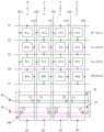
图2为本发明实施例一种显示面板的结构示意图,以第一~第四显示行和第一~第四显示列的结构作为示例。如图2所示,显示面板包括M+1条栅线和N对数据线,M+1条栅线和N对数据线交叉限定出呈阵列方式排布的M*N个显示单元,每对数据线包括第一数据线和第二数据线。FIG. 2 is a schematic structural diagram of a display panel according to an embodiment of the present invention, taking the structures of the first to fourth display rows and the first to fourth display columns as an example. As shown in FIG. 2 , the display panel includes M+1 gate lines and N pairs of data lines. The intersection of M+1 gate lines and N pairs of data lines defines M*N display units arranged in an array. The data lines include first data lines and second data lines.
第m显示行中,奇数显示列的显示单元与第m条栅线连接,偶数显示列的显示单元与第m+1条栅线连接;第n显示列中,奇数显示行的显示单元与第n对数据线的第一数据线连接,偶数显示行的显示单元与第n对数据线的第二数据线连接。其中,M和N为大于等于2的偶数,m=1,2,……,M,n=1,2,……,N。In the mth display row, the display cells of the odd-numbered display columns are connected to the mth gate line, and the display cells of the even-numbered display columns are connected to the m+1th gate line; in the nth display column, the display cells of the odd-numbered display rows are connected to the mth gate line. The first data lines of the n pairs of data lines are connected, and the display units of the even-numbered display lines are connected to the second data lines of the nth pair of data lines. Wherein, M and N are even numbers greater than or equal to 2, m=1, 2, ..., M, n=1, 2, ..., N.
平行设置的M+1条栅线(G1、G2、G3、G4……)限定出M个显示行,第m显示行由第m条栅线和第m+1条栅线限定,第m条栅线设置在第m显示行的上侧,第m+1条栅线设置在第m显示行的下侧,即第m条栅线设置在第m显示行远离第m+1显示行的一侧。或者说,在m=2,……,M时,第m条栅线设置在第m-1显示行与第m显示行之间,第m+1条栅线设置在第m显示行与第m+1显示行之间。例如,第三条栅线G3和第四条栅线G4限定出第三显示行,第三条栅线G3设置在第三显示行的上侧,第四条栅线G4设置在第四显示行的下侧。M+1 grid lines (G1, G2, G3, G4...) arranged in parallel define M display lines, the m th display line is defined by the m th grid line and the m+1 th grid line, and the m th The grid line is arranged on the upper side of the m-th display row, and the m+1-th grid line is arranged on the lower side of the m-th display row, that is, the m-th grid line is arranged on the m-th display row away from the m+1-th display row. side. In other words, when m=2,...,M, the mth grid line is set between the m-1th display row and the mth display row, and the m+1th grid line is set between the mth display row and the mth display row. m+1 shows between lines. For example, the third grid line G3 and the fourth grid line G4 define the third display row, the third grid line G3 is arranged on the upper side of the third display row, and the fourth grid line G4 is arranged on the fourth display row the underside.
平行设置的N对数据线(D1、D2、D3、D4……)中,每对数据线包括两条数据线,分别是第一数据线和第二数据线,第一数据线和第二数据线分别设置在每个显示列的两侧,第一数据线和第二数据线限定出所在的显示列。在n=1时,第一对数据线的第一数据线设置在第一显示列远离第二显示列的一侧。在n=2,……,N-1时,第n对数据线的第一数据线设置在第n-1显示列与第n显示列之间,第n对数据线的第二数据线设置在第n显示列与第n+1显示列之间。在n=N时,第N对数据线的第二数据线设置在第N显示列远离第N-1显示列的一侧。例如,第三对数据线D3包括第一数据线D31和第二数据线D32,第一数据线D31和第二数据线D32限定出第3显示列,第一数据线D31设置在第2显示列与第三显示列之间,第二数据线D32设置在第三显示列与第四显示列之间。In the N pairs of data lines (D1, D2, D3, D4...) arranged in parallel, each pair of data lines includes two data lines, respectively a first data line and a second data line, and a first data line and a second data line Lines are respectively arranged on both sides of each display column, and the first data line and the second data line define the display column in which the display column is located. When n=1, the first data line of the first pair of data lines is disposed on the side of the first display column away from the second display column. When n=2,...,N-1, the first data line of the nth pair of data lines is set between the n-1th display column and the nth display column, and the second data line of the nth pair of data lines is set Between the nth display column and the n+1th display column. When n=N, the second data line of the N-th pair of data lines is disposed on the side of the N-th display column away from the N-1-th display column. For example, the third pair of data lines D3 includes a first data line D31 and a second data line D32, the first data line D31 and the second data line D32 define a third display column, and the first data line D31 is arranged in the second display column and the third display column, the second data line D32 is disposed between the third display column and the fourth display column.
M个显示行中包括M/2个奇数显示行和M/2个偶数显示行,奇数显示行的显示单元和偶数显示行的显示单元分别连接不同的数据线。N个显示列中包括N/2个奇数显示列和N/2个偶数显示列,奇数显示列的显示单元和偶数显示列的显示单元分别连接不同的栅线。第m显示行中,奇数显示列的显示单元与第m条栅线连接,偶数显示列的显示单元与第m+1条栅线连接。第n显示列中,奇数显示行的显示单元与第n对数据线的第一数据线连接,偶数显示行的显示单元与第n对数据线的第二数据线连接。The M display lines include M/2 odd-numbered display lines and M/2 even-numbered display lines, and the display units of the odd-numbered display lines and the display units of the even-numbered display lines are respectively connected to different data lines. The N display columns include N/2 odd-numbered display columns and N/2 even-numbered display columns, and the display units of the odd-numbered display columns and the display units of the even-numbered display columns are respectively connected to different gate lines. In the m-th display row, the display cells of the odd-numbered display columns are connected to the m-th gate line, and the display cells of the even-numbered display columns are connected to the m+1-th gate line. In the nth display column, the display cells of the odd-numbered display row are connected to the first data line of the nth pair of data lines, and the display cells of the even-numbered display row are connected to the second data line of the nth pair of data lines.
下面以图2所示的第二显示行、第三显示行、第二显示列和第三显示列为例,说明各个显示单元的连接结构。The connection structure of each display unit is described below by taking the second display row, the third display row, the second display column and the third display column shown in FIG. 2 as an example.
第二显示行为偶数行,第二显示行中所有显示单元与该显示单元所在显示列的第二数据线连接。第二显示行中第一显示列的显示单元P21与第一显示列的第二数据线D12连接,第二显示行中第二显示列的显示单元P22与第二显示列的第二数据线D22连接,第二显示行中第三显示列的显示单元P31与第三显示列的第二数据线D32连接,第二显示行中第四显示列的显示单元P42与第四显示列的第二数据线D42连接。The second display row is an even-numbered row, and all the display units in the second display row are connected to the second data line of the display column where the display unit is located. The display unit P21 of the first display column in the second display row is connected to the second data line D12 of the first display column, and the display unit P22 of the second display column of the second display row is connected to the second data line D22 of the second display column connected, the display unit P31 of the third display column in the second display row is connected to the second data line D32 of the third display column, and the display unit P42 of the fourth display column in the second display row is connected to the second data line of the fourth display column Line D42 is connected.
第三显示行为奇数行,第三显示行中所有显示单元与该显示单元所在显示列的第一数据线连接。第三显示行中第一显示列的显示单元P31与第一显示列的第一数据线D11连接,第三显示行中第二显示列的显示单元P32与第二显示列的第一数据线D21连接,第三显示行中第三显示列的显示单元P33与第三显示列的第一数据线D31连接,第三显示行中第四显示列的显示单元P34与第四显示列的第一数据线D41连接。The third display row is an odd-numbered row, and all the display units in the third display row are connected to the first data line of the display column where the display unit is located. The display unit P31 of the first display column in the third display row is connected to the first data line D11 of the first display column, and the display unit P32 of the second display column of the third display row is connected to the first data line D21 of the second display column connected, the display unit P33 of the third display column in the third display row is connected to the first data line D31 of the third display column, and the display unit P34 of the fourth display column in the third display row is connected to the first data line of the fourth display column Line D41 is connected.
第二显示列为偶数列,第二显示列中所有显示单元与该显示单元所在行下方的栅线连接。第二显示列中第一显示行的显示单元P12与第一显示行下方的第二栅线G2连接,第二显示列中第二显示行的显示单元P22与第二显示行下方的第三栅线G3连接,第二显示列中第三显示行的显示单元P32与第三显示行下方的第四栅线G4连接,第二显示列中第四显示行的显示单元P42与第四显示行下方的第五栅线G5连接。The second display column is an even-numbered column, and all the display units in the second display column are connected to the gate lines below the row where the display unit is located. The display cell P12 of the first display row in the second display column is connected to the second gate line G2 below the first display row, and the display cell P22 of the second display row of the second display column is connected to the third gate line below the second display row The line G3 is connected, the display unit P32 of the third display row in the second display column is connected to the fourth gate line G4 below the third display row, and the display unit P42 of the fourth display row in the second display column is connected to the bottom of the fourth display row. The fifth gate line G5 is connected.
第三显示列为奇数列,第三显示列中所有显示单元与该显示单元所在行上方的栅线连接。第三显示列中第一显示行的显示单元P13与第一显示行上方的第一栅线G1连接,第三显示列中第二显示行的显示单元P23与第二显示行上方的第二栅线G2连接,第三显示列中第三显示行的显示单元P33与第三显示行上方的第三栅线G3连接,第三显示列中第四显示行的显示单元P43与第四显示行上方的第四栅线G4连接。The third display column is an odd-numbered column, and all the display units in the third display column are connected to the gate lines above the row where the display unit is located. The display cell P13 of the first display row in the third display column is connected to the first gate line G1 above the first display row, and the display cell P23 of the second display row of the third display column is connected to the second gate line above the second display row The line G2 is connected, the display unit P33 of the third display row in the third display column is connected to the third gate line G3 above the third display row, and the display unit P43 of the fourth display row in the third display column is connected to the top of the fourth display row. The fourth gate line G4 is connected.
本发明实施例中,显示面板包括显示区域和外围区域,外围区域设置在显示区域的外围,M*N个显示单元设置在显示区域。本发明实施例显示面板还包括数据控制器100,数据控制器100设置在外围区域,与N对数据线中第一数据线和第二数据线连接,用于使相邻的显示列之间的第一数据线和第二数据线同时向显示单元写入显示数据。In the embodiment of the present invention, the display panel includes a display area and a peripheral area, the peripheral area is arranged at the periphery of the display area, and M*N display units are arranged in the display area. The display panel according to the embodiment of the present invention further includes a
如图2所示,数据控制器100包括第一多路开关10、第二多路开关20、第一控制线30和第二控制线40,第一控制线30和第二控制线40用于按照预设时序,导通第一多路开关10中所有开关,关断第二多路开关20中所有开关;或者用于按照预设时序,关断第一多路开关10中所有开关,导通第二多路开关20中所有开关。第一多路开关10包括N个开关,N个开关的控制端均与第一控制线30连接,由第一控制线30控制第一多路开关10中的N个开关同时导通或同时关断,使奇数显示列的第一数据线和偶数显示列的第二数据线同时向显示单元写入显示数据。第二多路开关20包括N个开关,N个开关的控制端均与第二控制线40连接,由第二控制线40控制第二多路开关20中的N个开关同时导通或同时关断,使奇数显示列的第二数据线和偶数显示列的第一数据线同时向显示单元写入显示数据。As shown in FIG. 2, the
本发明实施例中,第一多路开关10包括N/2个第一开关T1和N/2个第二开关T2,第二多路开关20包括N/2个第一开关T1和N/2个第二开关T2。第一控制线30和第二控制线40用于按照预设时序,在一个行周期中,导通第一多路开关10中所有的第一开关T1和第二开关T2,关断第二多路开关20中所有的第一开关T1和第二开关T2,在另一个行周期中,导通第二多路开关20中所有的第一开关T1和第二开关T2,关断第一多路开关10中所有的第一开关T1和第二开关T2。In this embodiment of the present invention, the
第一多路开关10中,N/2个第一开关T1分别与奇数显示列的第一数据线连接,用于按照预设时序导通,使第一数据线向该奇数显示列中奇数显示行的显示单元写入显示数据;N/2个第二开关T2分别与偶数显示列的第二数据线连接,用于按照预设时序导通,使第二数据线向该偶数显示列中偶数显示行的显示单元写入显示数据。如图2所述,第一多路开关10中的一个第一开关T1与第一显示列的第一数据线D11连接,可以使第一数据线D11向第一显示列中奇数显示行的显示单元P11和显示单元P31写入显示数据。第一多路开关10中的另一个第一开关T1与第三显示列的第一数据线D31连接,可以使第一数据线D31向第三显示列中奇数显示行的显示单元P13和显示单元P33写入显示数据。第一多路开关10中的一个第二开关T2与第二显示列的第二数据线D22连接,可以使第二数据线D22向第二显示列中偶数显示行的显示单元P22和显示单元P42写入显示数据。第一多路开关10中的另一个第二开关T2与第四显示列中的第二数据线D42连接,可以使第二数据线D42向第四显示列中偶数显示行的显示单元P24和显示单元P44写入显示数据。In the
第二多路开关20中,N/2个第一开关T1分别与偶数显示列的第一数据线连接,用于按照预设时序导通,使第一数据线向该偶数显示列中奇数显示行的显示单元写入显示数据;N/2个第二开关T2分别与奇数显示列的第二数据线连接,用于按照预设时序导通,使第二数据线向奇数显示列中偶数显示行的显示单元写入显示数据。如图2所述,第二多路开关20中的一个第一开关T1与第二显示列的第一数据线D21连接,可以使第一数据线D21向第二显示列中奇数显示行的显示单元P12和显示单元P32写入显示数据。第二多路开关20中的另一个第一开关T1与第四显示列的第一数据线D41连接,可以使第一数据线D41向第四显示列中奇数显示行的显示单元P14和显示单元P34写入显示数据。第二多路开关20中的一个第二开关T2与第一显示列的第二数据线D12连接,可以使第二数据线D12向第一显示列中偶数显示行的显示单元P21和显示单元P41写入显示数据。第二多路开关20中的另一个第二开关T2与第三显示列的第二数据线D32连接,可以使第二数据线D32向第三显示列中偶数显示行的显示单元P23和显示单元P43写入显示数据。In the
下面通过显示面板的驱动过程的示例说明本发明实施例的技术方案。The technical solutions of the embodiments of the present invention are described below by using an example of a driving process of a display panel.
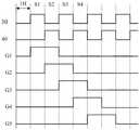
图3为本发明实施例显示面板的一种工作时序图,示意了第一显示行~第四显示行的驱动时序,栅线的扫描信号为高电平信号,第一多路开关和第二多路开关的导通信号为高电平信号,H为行周期,也称之为显示数据的写入时间。3 is a working timing diagram of a display panel according to an embodiment of the present invention, illustrating the driving timing of the first display row to the fourth display row, the scanning signal of the gate line is a high level signal, the first multiplexer and the second The turn-on signal of the multiplexer is a high-level signal, and H is the line period, which is also called the writing time of the display data.
如图3所示,每条栅线在2个行周期H内输出扫描信号,相邻栅线输出扫描信号的起始时刻间隔1个行周期H,使相邻栅线所输出的扫描信号存在1个行周期H的重叠。As shown in FIG. 3 , each gate line outputs a scan signal within 2 line periods H, and the start time of the adjacent gate line outputting the scan signal is separated by 1 line period H, so that the scan signal output by the adjacent gate line exists 1 line period H overlap.
在m=2,……,M时,第m栅线在2个行周期H内输出扫描信号期间,在第一个行周期H,第m-1栅线G仍在输出扫描信号,在第2个行周期H,第m+1栅线开始输出扫描信号,第m-1栅线输出的扫描信号与第m栅线输出的扫描信号有1个行周期H的重叠,第m栅线G输出的扫描信号与第m+1栅线输出的扫描信号有1个行周期H的重叠。When m=2,...,M, during the period when the m-th gate line outputs the scan signal in 2 line periods H, in the first line period H, the m-1-th gate line G still outputs the scan signal. 2 line periods H, the m+1th gate line starts to output the scan signal, the scan signal output by the m-1th gate line and the scan signal output by the mth gate line overlap by one line period H, the mth gate line G The output scan signal overlaps with the scan signal output from the m+1 th gate line by one line period H.
在m=1时,第一栅线在2个行周期H内输出扫描信号期间,在第1个行周期H,没有其它栅线输出扫描信号;在第2个行周期H,第二栅线开始输出扫描信号,即第一栅线输出的扫描信号与第二栅线输出的扫描信号在第2个行周期H内重叠。When m=1, during the period when the first gate line outputs the scan signal in 2 line periods H, in the first line period H, no other gate line outputs the scan signal; in the second line period H, the second gate line Start to output the scan signal, that is, the scan signal output by the first gate line and the scan signal output by the second gate line overlap in the second line period H.
如图3所示,每条栅线输出扫描信号期间,一个多路开关从导通状态切换为关断状态,另一个多路开关从关断状态切换为导通状态,即两个多路开关是分时导通的。在第一栅线G1输出扫描信号的2个行周期H内,在第1个行周期H,第一多路开关10处于导通状态,第二多路开关20处于关断状态;在第2个行周期H,第一多路开关10处于关断状态,第二多路开关20处于导通状态。在第二栅线G2输出扫描信号的2个行周期H内,在第1个行周期H,第一多路开关10处于关断状态,第二多路开关20处于导通状态;在第2个行周期H,第一多路开关10处于导通状态,第二多路开关20处于关断状态。在第三栅线G3输出扫描信号的2个行周期H内,在第1个行周期H,第一多路开关10处于导通状态,第二多路开关20处于关断状态;在第2个行周期H,第一多路开关10处于关断状态,第二多路开关20处于导通状态。在第四栅线G4输出扫描信号的2个行周期H内,在第1个行周期H,第一多路开关10处于关断状态,第二多路开关20处于导通状态;在第2个行周期H,第一多路开关10处于导通状态,第二多路开关20处于关断状态。As shown in Figure 3, during the period when each gate line outputs the scan signal, one multiplexer switches from the on state to the off state, and the other multiplexer switches from the off state to the on state, that is, two multiplexers It is time-sharing conduction. In the 2 line periods H in which the first gate line G1 outputs the scan signal, in the first line period H, the
如图3所示,在4个行周期H内,本发明实施例显示面板的驱动过程包括:As shown in FIG. 3 , within four line periods H, the driving process of the display panel according to the embodiment of the present invention includes:
1、在S1时段(t=0~H),第一栅线G1输出扫描信号,第一控制线30向第一多路开关10输出导通信号,第二控制线40向第二多路开关20输出关断信号。1. In the S1 period (t=0~H), the first gate line G1 outputs a scan signal, the
虽然第一多路开关10所控制的第一开关T1和第二开关T2都导通,但由于第一栅线G1与第一显示行中奇数显示列的显示单元(P11和P13)连接,因而只有第一开关T1所连接的第一数据线(D11和D31)向第一显示行中奇数显示列的显示单元(P11和P13)写入显示数据,第二开关T2所连接的第二数据线(D22和D42)不能向任何显示单元写入显示数据。Although the first switch T1 and the second switch T2 controlled by the
2、在S2时段(t=H~2H),第一栅线G1输出扫描信号,第二栅线G2输出扫描信号,第一控制线30向第一多路开关10输出关断信号,第二控制线40向第二多路开关20输出导通信号。2. In the S2 period (t=H~2H), the first gate line G1 outputs a scan signal, the second gate line G2 outputs a scan signal, the
第二多路开关20所控制的第一开关T1和第二开关T2都导通,由于第二栅线G2分别与第一显示行中偶数显示列的显示单元(P12和P14)和第二显示行中奇数显示列的显示单元(P21和P23)连接,因此第一开关T1所连接的第一数据线(D21和D41)向第一显示行中偶数显示列的显示单元(P12和P14)写入显示数据,第二开关T2所连接的第二数据线(D12和D32)向第二显示行中奇数显示列的显示单元(P21和P23)写入显示数据。The first switch T1 and the second switch T2 controlled by the
3、在S3时段(t=2H~3H),第二栅线G2输出扫描信号,第三栅线G3输出扫描信号,第一控制线30向第一多路开关10输出导通信号,第二控制线40向第二多路开关20输出关断信号。3. During the S3 period (t=2H-3H), the second gate line G2 outputs a scan signal, the third gate line G3 outputs a scan signal, the
第一多路开关10所控制的第一开关T1和第二开关T2都导通,由于第三栅线G3分别与第二显示行中偶数显示列的显示单元(P22和P24)和第三显示行中奇数显示列的显示单元(P31和P33)连接,因此第一开关T1所连接的(D11和D31)向第三显示行中奇数显示列的显示单元(P31和P33)写入显示数据,第二开关T2所连接的第二数据线(D22和D42)向第二显示行中偶数显示列的显示单元(P22和P24)写入显示数据。The first switch T1 and the second switch T2 controlled by the
4、在S4时段(t=3H~4H),第三栅线G3输出扫描信号,第四栅线G4输出扫描信号,第一控制线30向第一多路开关10输出关断信号,第二控制线40向第二多路开关20输出导通信号。4. During the S4 period (t=3H~4H), the third gate line G3 outputs a scan signal, the fourth gate line G4 outputs a scan signal, the
第二多路开关20所控制的第一开关T1和第二开关T2都导通,由于第四栅线G4分别与第三显示行中偶数显示列的显示单元(P32和P34)和第四显示行中奇数显示列的显示单元(P41和P43)连接,因此第一开关T1所连接的第一数据线(D21和D41)向第三显示行中偶数显示列的显示单元(P32和P34)写入显示数据,第二开关T2所连接的第二数据线(D12和D32)向第四显示行中奇数显示列的显示单元(P41和P43)写入显示数据。The first switch T1 and the second switch T2 controlled by the
从第m条栅线的驱动来看,在第m条栅线输出扫描信号的2个行周期H时间内,在第1个行周期H,一个多路开关处于导通状态,在第2个行周期H,另一个多路开关处于导通状态。在第1个行周期H中,第m显示行中奇数显示列的显示单元写入显示数据,第m-1显示行中偶数显示列的显示单元写入显示数据。在第2个行周期H中,第m显示行中偶数显示列的显示单元写入显示数据,第m+1显示行中奇数显示列的显示单元写入显示数据。From the point of view of the driving of the mth gate line, within the 2 line periods H during which the mth gate line outputs the scan signal, in the first line period H, a multiplexer is in the conducting state, and in the second line period H Line period H, the other multiplexer is in the conducting state. In the first line period H, display data is written to the display cells of the odd-numbered display columns in the m-th display row, and display data is written to the display cells of the even-numbered display columns of the m-1th display row. In the second line period H, display data is written to the display cells of the even-numbered display columns in the m-th display row, and display data is written to the display cells of the odd-numbered display columns of the m+1-th display row.
当第m条栅线为奇数栅线时,在其输出扫描信号的2个行周期H时间内,在第1个行周期H,第一多路开关10处于导通状态,第二多路开关20处于关断状态;在第2个行周期H,第一多路开关10处于关断状态,第二多路开关20处于导通状态。在第一个行周期H中,第m显示行中奇数显示列的显示单元写入显示数据,第m-1显示行中偶数显示列的显示单元写入显示数据。在第2个行周期H中,第m显示行中偶数显示列的显示单元写入显示数据,第m+1显示行中奇数显示列的显示单元写入显示数据。When the m-th gate line is an odd-numbered gate line, within the 2 line periods H of outputting the scan signal, in the first line period H, the
当第m条栅线为偶数栅线时,在其输出扫描信号的2个行周期H时间内,在第1个行周期H,第一多路开关10处于关断状态,第二多路开关20处于导通状态;在第2个行周期H,第一多路开关10处于导通状态,第二多路开关20处于关断状态。在第1个行周期H中,第m显示行中奇数显示列的显示单元写入显示数据,第m-1显示行中偶数显示列的显示单元写入显示数据。在第2个行周期H中,第m显示行中偶数显示列的显示单元写入显示数据,第m+1显示行中奇数显示列的显示单元写入显示数据。When the m-th gate line is an even-numbered gate line, within the 2 line periods H of outputting the scan signal, in the first line period H, the
在示例性实施方式中,数据控制器可以采用数据选择器(Multiplexer,简称MUX),栅线的扫描信号可以是高电平信号,或者可以是低电平信号,第一多路开关和第二多路开关的导通信号可以是高电平信号,或者可以是低电平信号。In an exemplary embodiment, the data controller may use a data selector (Multiplexer, MUX for short), the scan signal of the gate line may be a high-level signal, or may be a low-level signal, the first multiplexer and the second The turn-on signal of the multiplexer may be a high-level signal, or may be a low-level signal.
从本发明实施例显示面板的结构以及驱动过程可以看出,本发明实施例通过设置显示单元的排列方式和驱动方式,不仅使得每个显示行中奇数显示列的显示单元和偶数显示列的显示单元在不同时段写入(分时写入)显示数据,而且使得相邻显示列之间的第一数据线和第二数据线在相同时段写入(同时写入)显示数据。在m=2,……,M时,由于每条栅线在2个行周期H内输出扫描信号,且相邻栅线具有1个行周期H的扫描信号重叠,因而在第m条栅线输出扫描信号的第1个行周期H内,第一数据线向第m显示行中奇数显示列的显示单元写入显示数据,第二数据线向第m-1显示行中偶数显示列的显示单元写入显示数据;在第m条栅线输出扫描信号的第2个行周期H内,第一数据线向第m+1显示行中奇数显示列的显示单元写入显示数据,第二数据线向第m显示行中偶数显示列的显示单元写入显示数据。由此可见,第m显示行中奇数显示列的显示单元在第1个行周期H内写入显示数据,第m显示行中偶数显示列的显示单元在第2个行周期H内写入显示数据,因而实现了一个显示行中奇数显示列的显示单元和偶数显示列的显示单元分时写入。在每个行周期H内,均是同时向奇数显示列的显示单元和偶数显示列的显示单元写入显示数据,因而实现了相邻显示列之间的第一数据线和第二数据线同时写入。It can be seen from the structure and driving process of the display panel in the embodiment of the present invention that by setting the arrangement and driving mode of the display units in the embodiment of the present invention, not only the display units of the odd-numbered display columns and the even-numbered display columns of each display row are displayed The cells write (time-division writing) display data in different time periods, and cause the first data line and the second data line between adjacent display columns to write (simultaneously write) display data in the same time period. When m=2,...,M, since each gate line outputs a scan signal within 2 line periods H, and adjacent gate lines have scan signals of 1 line period H overlap, the m-th gate line In the first line period H of outputting the scan signal, the first data line writes display data to the display unit of the odd-numbered display column in the m-th display line, and the second data line writes the display data to the display unit of the even-numbered display column in the m-1th display line. The unit writes display data; in the second row period H of the mth gate line outputting the scan signal, the first data line writes display data to the display unit of the odd display column in the m+1th display row, and the second data The line writes display data to the display cells of the even-numbered display columns in the mth display row. It can be seen that the display cells of the odd-numbered display columns in the m-th display row write display data in the first row period H, and the display cells of the even-numbered display columns in the m-th display row write display data in the second row period H data, thus realizing a time-sharing writing of the display cells of the odd-numbered display columns and the display cells of the even-numbered display columns in a display row. In each row period H, display data is simultaneously written to the display cells of odd-numbered display columns and the display cells of even-numbered display columns, so that the first data line and the second data line between adjacent display columns can be simultaneously write.
传统结构的显示面板中,一个显示列的所有显示单元共用一条数据线,数据线上数据电压的保持时间为1H,像素驱动电路通过数据线对驱动薄膜晶体管(TFT)的栅极进行充电即Vth补偿时,补偿时间等于数据电压保持时间,即保持时间为1H。本发明实施例中,由于每个显示列中奇数显示行的显示单元和偶数显示行的显示单元分别连接不同的数据线,数据线上数据电压的保持时间为2H,补偿时间增加了1H,因而增加了像素驱动电路阈值电压的补偿时间,可以满足较高刷新频率下阈值电压的补偿能力,有效解决了较高刷新频率显示面板存在阈值电压补偿能力不足的问题。由于位于相邻显示列之间的第一数据线和第二数据线同时写入,避免了一条数据线处于写入状态时而另一条数据线处于浮空状态的情形,因而消除了相邻数据线上电位相互影响的因素,有效解决了显示面板存在显示不良的问题。In a display panel with a traditional structure, all display units in a display column share a data line, the data voltage on the data line is held for 1H, and the pixel driving circuit charges the gate of the driving thin film transistor (TFT) through the data line, which is Vth. During compensation, the compensation time is equal to the data voltage holding time, that is, the holding time is 1H. In the embodiment of the present invention, since the display units of the odd-numbered display rows and the display units of the even-numbered display rows in each display column are respectively connected to different data lines, the holding time of the data voltage on the data lines is 2H, and the compensation time is increased by 1H. The compensation time for the threshold voltage of the pixel driving circuit is increased, which can satisfy the compensation capability of the threshold voltage at a higher refresh frequency, and effectively solve the problem of insufficient threshold voltage compensation capability of the display panel with a higher refresh frequency. Since the first data line and the second data line located between adjacent display columns are written at the same time, the situation that one data line is in the writing state and the other data line is in the floating state is avoided, thus eliminating the adjacent data lines The factors influencing each other on the upper potential effectively solve the problem of poor display on the display panel.
对于图1所示的显示面板,虽然可以通过增加相邻数据线之间的距离来降低寄生电容,但该方式不仅降低了开口率,而且受工艺过程中对位偏差的影响,像素布局容易产生其它显示不良,降低了良品率。由于本发明实施例中奇数显示列的显示单元和偶数显示列的显示单元分别连接不同的栅线,奇数显示行的显示单元和偶数显示行的显示单元分别连接不同的数据线,像素结构及其连接关系整齐、规则和清晰,不仅简化了显示面板的结构设计,降低了像素排布难度,而且减少了制备过程的工艺缺陷,提高了生产质量,有效保证了良品率。本发明实施例显示面板的制备过程不需要改变现有工艺流程,不需改变现有工艺设备,没有增加新的工艺以及引入新的材料,工艺兼容性好,工艺可实现性高,实用性强,具有良好的应用前景。For the display panel shown in FIG. 1, although the parasitic capacitance can be reduced by increasing the distance between adjacent data lines, this method not only reduces the aperture ratio, but also is affected by the alignment deviation during the process, and the pixel layout is prone to occur. Others display poor, reducing the yield. Since the display units of the odd-numbered display columns and the display units of the even-numbered display columns in the embodiment of the present invention are respectively connected to different gate lines, the display units of the odd-numbered display rows and the display units of the even-numbered display rows are respectively connected to different data lines, the pixel structure and its structure. The connection relationship is neat, regular and clear, which not only simplifies the structural design of the display panel, reduces the difficulty of pixel arrangement, but also reduces the process defects in the preparation process, improves the production quality, and effectively ensures the yield. The preparation process of the display panel according to the embodiment of the present invention does not need to change the existing process flow, does not need to change the existing process equipment, does not add new processes or introduce new materials, has good process compatibility, high process achievability, and strong practicability , has a good application prospect.
综上,本发明实施例提供的显示面板,通过设置显示单元的排列方式和驱动方式,奇数显示列的显示单元和偶数显示列的显示单元分别连接不同的栅线,奇数显示行的显示单元和偶数显示行的显示单元分别连接不同的数据线,使得同一显示行中奇数显示列的显示单元和偶数显示列的显示单元分时写入显示数据,相邻显示列之间的第一数据线和第二数据线同时写入显示数据,不仅有效解决了较高刷新频率显示面板存在阈值电压补偿能力不足的问题,保证了显示效果,而且有效解决了相邻数据线上电位相互影响的问题,提高了显示品质。To sum up, in the display panel provided by the embodiment of the present invention, by setting the arrangement mode and driving mode of the display units, the display units of the odd-numbered display columns and the display units of the even-numbered display columns are respectively connected to different gate lines, and the display units of the odd-numbered display rows and The display units of the even-numbered display rows are respectively connected to different data lines, so that the display units of the odd-numbered display columns and the display units of the even-numbered display columns in the same display row write display data in a time-sharing manner, and the first data lines between adjacent display columns and The second data line writes display data at the same time, which not only effectively solves the problem of insufficient threshold voltage compensation capability of the display panel with a higher refresh frequency, and ensures the display effect, but also effectively solves the problem of the potential interaction between adjacent data lines. display quality.
图4为本发明实施例显示面板的另一种工作时序图。图3所示的工作时序中,每条栅线输出扫描信号的电平宽度为2倍的行周期H,第一控制线和第二控制线输出导通信号或关断信号的电平宽度为1倍的行周期H。本实施例显示面板的结构与前述实施例相同,与前述实施例不同的是,本实施例中每条栅线输出扫描信号的电平宽度为2H-(a+b),第一控制线和第二控制线输出导通信号的电平宽度为H-c,第一控制线和第二控制线输出关断信号的电平宽度为H+c,如图4所示。在4个行周期H内,本实施例显示面板的工作时序包括:FIG. 4 is another working timing diagram of the display panel according to the embodiment of the present invention. In the working sequence shown in FIG. 3 , the level width of the output scan signal of each gate line is 2 times the line period H, and the level width of the output turn-on signal or turn-off signal of the first control line and the second control line is 1 times the line period H. The structure of the display panel of this embodiment is the same as that of the previous embodiment, and the difference from the previous embodiment is that the level width of the output scan signal of each gate line in this embodiment is 2H-(a+b), and the first control line and The level width of the turn-on signal output by the second control line is H-c, and the level width of the turn-off signal output by the first control line and the second control line is H+c, as shown in FIG. 4 . In 4 line periods H, the working sequence of the display panel of this embodiment includes:
1、在S1时段(t=0~H),第一栅线G1在a~H时段内输出扫描信号,第一控制线30在0~(H-c)时段内输出导通信号,在(H-c)~H时段内输出关断信号,第二控制线40在0~H时段内输出关断信号。1. In the S1 period (t=0~H), the first gate line G1 outputs the scan signal in the a~H period, the
2、在S2时段(t=H~2H),第一栅线G1在H~(2H-b)时段内输出扫描信号,第二栅线G2在(H+a)~2H时段内输出扫描信号,第一控制线30在H~2H时段内输出关断信号,第二控制线40在H~(2H-c)时段内输出导通信号,在(2H-c)~2H时段内输出关断信号。2. In the S2 period (t=H~2H), the first gate line G1 outputs the scan signal in the H~(2H-b) period, and the second gate line G2 outputs the scan signal in the (H+a)~2H period , the
3、在S3时段(t=2H~3H),第二栅线G2在2H~(3H-b)时段内输出扫描信号,第三栅线G3在(2H+a)~3H时段内输出扫描信号,第一控制线30在2H~(3H-c)时段内输出导通信号,在(3H-c)~3H时段内输出关断信号,第二控制线40在2H~3H时段内输出关断信号。3. In the S3 period (t=2H~3H), the second gate line G2 outputs the scan signal in the 2H~(3H-b) period, and the third gate line G3 outputs the scan signal in the (2H+a)~3H period , the
4、在S4时段(t=3H~4H),第三栅线G3在3H~(4H-b)时段内输出扫描信号,第四栅线G4在(3H+a)~4H时段内输出扫描信号,第一控制线30在3H~4H时段内输出关断信号,第二控制线40在3H~(4H-c)时段内输出导通信号,在(4H-c)~4H时段内输出关断信号。4. In the S4 period (t=3H~4H), the third gate line G3 outputs the scan signal in the 3H~(4H-b) period, and the fourth gate line G4 outputs the scan signal in the (3H+a)~4H period , the
在每个时段,第一控制线30或第二控制线40输出的导通信号的宽度为H-c,输出的关断信号的宽度为H,第一控制线30和第二控制线40均以宽度为H-c的导通信号和宽度为H+c的关断信号的周期性波形进行输出。每条栅线输出扫描信号的电平宽度为2H-(a+b),扫描信号在第一控制线30或第二控制线40输出导通信号后的a时刻开始输出,在输出扫描信号的电平宽度达到2H-(a+b)时停止输出。这样,控制线输出导通信号的时间早于栅线输出扫描信号的时间,使得第一多路开关或第二多路开关连接的数据线所传输的显示数据稳定后,才输出扫描信号使显示数据写入相应的显示单元,保证了显示数据写入的准确定,保证了显示效果。在一些可能的实现方式中,a、b和c可以根据实际需要设置,可以是a=b,或者可以是a=c,或者可以是b=c,或者可以是a=b=c。In each period, the width of the turn-on signal output by the
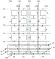
图5为本发明实施例另一种显示面板的结构示意图,示意了第一~第四显示行和第一~第四显示列的结构。如图5所示,显示面板包括M+1条栅线和N对数据线,M+1条栅线和N对数据线交叉限定出呈阵列方式排布的M*N个显示单元,每对数据线包括第一数据线和第二数据线。第m显示行中,偶数显示列的显示单元与第m条栅线连接,奇数显示列的显示单元与第m+1条栅线连接;第n显示列中,偶数显示行的显示单元与第n对数据线的第一数据线连接,奇数显示行的显示单元与第n对数据线的第二数据线连接。其中,M和N为大于等于2的偶数,m=1,2,……,M,n=1,2,……,N。如图5所示,奇数显示行的显示单元和偶数显示行的显示单元分别连接不同的数据线,奇数显示列的显示单元和偶数显示列的显示单元分别连接不同的栅线。本实施例数据控制器100的结构和驱动过程与前述实施例基本上相同,这里不再赘述。FIG. 5 is a schematic structural diagram of another display panel according to an embodiment of the present invention, illustrating the structures of the first to fourth display rows and the first to fourth display columns. As shown in FIG. 5 , the display panel includes M+1 gate lines and N pairs of data lines. The intersection of M+1 gate lines and N pairs of data lines defines M*N display units arranged in an array. The data lines include first data lines and second data lines. In the mth display row, the display cells of the even-numbered display columns are connected to the mth gate line, and the display cells of the odd-numbered display columns are connected to the m+1th gate line; in the nth display column, the display cells of the even-numbered display rows are connected to the mth gate line. The first data lines of the n pairs of data lines are connected, and the display units of the odd-numbered display rows are connected to the second data lines of the nth pair of data lines. Wherein, M and N are even numbers greater than or equal to 2, m=1, 2, ..., M, n=1, 2, ..., N. As shown in FIG. 5 , display cells in odd display rows and display cells in even display rows are respectively connected to different data lines, and display cells in odd display columns and display cells in even display columns are respectively connected to different gate lines. The structure and driving process of the
本发明实施例还提供了一种显示面板的驱动方法,显示面板采用前述任一个实施例的显示面板。本发明实施例显示面板的驱动方法包括:在m=2,……,M时,Embodiments of the present invention also provide a method for driving a display panel, where the display panel adopts the display panel of any one of the foregoing embodiments. The driving method of the display panel according to the embodiment of the present invention includes: when m=2, ..., M,
S1、向第m-1条栅线和第m条栅线输出扫描信号,向第m显示行中奇数显示列的显示单元和第m-1显示行中偶数显示列的显示单元写入显示数据;S1. Output scan signals to the m-1 th gate line and the m th gate line, and write display data to the display cells of the odd display columns in the m th display row and the display cells of the even display columns in the m-1 th display row ;
S2、向第m条栅线和第m+1条栅线输出扫描信号,向第m显示行中偶数显示列的显示单元和第m+1显示行中奇数显示列的显示单元写入显示数据。S2, output the scan signal to the mth gate line and the m+1th gate line, and write display data to the display cells of the even display columns in the mth display row and the display cells of the odd display columns in the m+1th display row .
在一种示例性实施方式中,步骤S1包括:In an exemplary embodiment, step S1 includes:
向第m-1条栅线和第m条栅线输出扫描信号,第一控制线向第一多路开关输出导通信号,第二控制线向第二多路开关输出关断信号,与所述第一多路开关连接的第一数据线向第m显示行中奇数显示列的显示单元写入显示数据,与所述第一多路开关连接的第二数据线向第m-1显示行中偶数显示列的显示单元写入显示数据。The scan signal is output to the m-1th gate line and the mth gate line, the first control line outputs a turn-on signal to the first multiplexer, and the second control line outputs a turn-off signal to the second multiplexer, which is consistent with all The first data line connected to the first multiplexer writes display data to the display units of the odd-numbered display columns in the mth display row, and the second data line connected to the first multiplexer writes display data to the m-1th display row Display data is written to the display cells of the even-numbered display column.
在一种示例性实施方式中,步骤S2包括:In an exemplary embodiment, step S2 includes:
向第m条栅线和第m+1条栅线输出扫描信号,第一控制线向第一多路开关输出关断信号,第二控制线向第二多路开关输出导通信号,与所述第二多路开关连接的第一数据线向第m显示行中偶数显示列的显示单元写入显示数据,与所述第二多路开关连接的第二数据线向第m+1显示行中奇数显示列的显示单元写入显示数据。The scan signal is output to the mth gate line and the m+1th gate line, the first control line outputs a turn-off signal to the first multiplexer, and the second control line outputs a turn-on signal to the second multiplexer, which is consistent with all The first data line connected to the second multiplexer writes display data to the display units of the even-numbered display columns in the mth display row, and the second data line connected to the second multiplexer writes display data to the m+1th display row Display data is written to display cells in odd-numbered display columns.
在一种示例性实施方式中,在2个行周期H内,向第m-1条栅线和第m条栅线输出扫描信号,包括:在t=0~H-b时段,向所述第m-1条栅线输出扫描信号,在t=a~H时段,向所述第m条栅线输出扫描信号;其中,a小于H,b小于H。In an exemplary embodiment, outputting the scan signal to the m-1 th gate line and the m th gate line within 2 row periods H includes: in the period of t=0˜H-b, sending the scan signal to the m th gate line -1 gate line outputs a scan signal, and in the period of t=a~H, outputs a scan signal to the mth gate line; wherein a is smaller than H, and b is smaller than H.
在一种示例性实施方式中,在2个行周期H内,向第m条栅线和第m+1条栅线输出扫描信号,包括:在t=H~(2H-b)时段,向第m条栅线输出扫描信号,在t=(H+a)~2H时段,向所述第m+1条栅线输出扫描信号。In an exemplary embodiment, within 2 row periods H, outputting scan signals to the m th gate line and the m+1 th gate line includes: in the period of t=H~(2H-b), to The m th gate line outputs a scan signal, and in the period of t=(H+a)˜2H, the scan signal is output to the m+1 th gate line.
在一种示例性实施方式中,在2个行周期H内,第一控制线向第一多路开关输出导通信号,第二控制线向第二多路开关输出关断信号,包括:第一控制线在0~(H-c)时段内向第一多路开关输出导通信号,第二控制线在0~H时段内向第二多路开关输出关断信号;其中,c小于H。In an exemplary implementation, within 2 row periods H, the first control line outputs a turn-on signal to the first multiplexer, and the second control line outputs a turn-off signal to the second multiplexer, including: a first A control line outputs a turn-on signal to the first multiplexer in the period of 0-(H-c), and the second control line outputs a turn-off signal to the second multiplexer in the period of 0-H; wherein, c is less than H.
在一种示例性实施方式中,在2个行周期H内,第一控制线向第一多路开关输出关断信号,第二控制线向第二多路开关输出导通信号,包括:第一控制线在H~2H时段内向第一多路开关输出关断信号,第二控制线在H~(2H-c)时段内向第二多路开关输出导通信号,在(2H-c)~2H时段内向第二多路开关输出关断信号;In an exemplary implementation, within 2 row periods H, the first control line outputs a turn-off signal to the first multiplexer, and the second control line outputs a turn-on signal to the second multiplexer, including: a first A control line outputs a turn-off signal to the first multiplexer during the H~2H period, the second control line outputs a turn-on signal to the second multiplexer during the H~(2H-c) period, and the (2H-c)~ Output a shutdown signal to the second multiplexer within the 2H period;
在一种示例性实施方式中,扫描信号的电平宽度为2H-(a+b)。In an exemplary embodiment, the level width of the scan signal is 2H-(a+b).
在一种示例性实施方式中,导通信号的电平宽度为H-c。In an exemplary embodiment, the level width of the turn-on signal is H-c.
在一种示例性实施方式中,所述驱动方法还包括:In an exemplary embodiment, the driving method further includes:
向第一栅线输出扫描信号,向第一显示行中奇数显示列的显示单元写入显示数据。A scan signal is output to the first gate line, and display data is written into the display cells of the odd-numbered display columns in the first display row.
本发明实施例提供了一种显示面板的驱动方法,通过设置显示单元的排列方式和驱动方式,奇数显示列的显示单元和偶数显示列的显示单元分别连接不同的栅线,奇数显示行的显示单元和偶数显示行的显示单元分别连接不同的数据线,使得同一显示行中奇数显示列的显示单元和偶数显示列的显示单元分时写入显示数据,相邻显示列之间的第一数据线和第二数据线同时写入显示数据,不仅有效解决了较高刷新频率显示面板存在阈值电压补偿能力不足的问题,保证了显示效果,而且有效解决了相邻数据线上电位相互影响的问题,提高了显示品质。An embodiment of the present invention provides a driving method for a display panel. By setting the arrangement mode and driving mode of the display units, the display units of the odd-numbered display columns and the display units of the even-numbered display columns are respectively connected to different gate lines, and the display units of the odd-numbered display rows are respectively connected to different gate lines. The unit and the display unit of the even-numbered display row are respectively connected to different data lines, so that the display unit of the odd-numbered display column and the display unit of the even-numbered display column in the same display row write display data in time-sharing, and the first data between adjacent display columns The display data is written into the second data line at the same time, which not only effectively solves the problem of insufficient threshold voltage compensation capability of the display panel with a higher refresh rate, ensures the display effect, but also effectively solves the problem of the mutual influence of the potentials on the adjacent data lines. , which improves the display quality.
基于前述实施例的发明构思,本发明实施例还提供了一种显示装置,显示装置包括采用前述实施例的显示面板。显示装置可以为:手机、平板电脑、电视机、显示器、笔记本电脑、数码相框、导航仪等任何具有显示功能的产品或部件。Based on the inventive concept of the foregoing embodiments, an embodiment of the present invention further provides a display device, which includes the display panel using the foregoing embodiments. The display device can be any product or component that has a display function, such as a mobile phone, a tablet computer, a TV, a monitor, a notebook computer, a digital photo frame, and a navigator.
虽然本发明所揭露的实施方式如上,但所述的内容仅为便于理解本发明而采用的实施方式,并非用以限定本发明。任何本发明所属领域内的技术人员,在不脱离本发明所揭露的精神和范围的前提下,可以在实施的形式及细节上进行任何的修改与变化,但本发明的专利保护范围,仍须以所附的权利要求书所界定的范围为准。Although the embodiments disclosed in the present invention are as above, the described contents are only the embodiments adopted to facilitate the understanding of the present invention, and are not intended to limit the present invention. Any person skilled in the art to which the present invention belongs, without departing from the spirit and scope disclosed by the present invention, can make any modifications and changes in the form and details of the implementation, but the scope of the patent protection of the present invention still needs to be The scope defined by the appended claims shall prevail.
Claims (14)
Translated fromChinesePriority Applications (3)
| Application Number | Priority Date | Filing Date | Title |
|---|---|---|---|
| CN202010167914.2ACN111243441B (en) | 2020-03-11 | 2020-03-11 | Display panel, driving method thereof and display device |
| US17/415,717US11972711B2 (en) | 2020-03-11 | 2020-12-29 | Display panel, drive method thereof and display apparatus |
| PCT/CN2020/140683WO2021179749A1 (en) | 2020-03-11 | 2020-12-29 | Display panel and driving method therefor, and display device |
Applications Claiming Priority (1)
| Application Number | Priority Date | Filing Date | Title |
|---|---|---|---|
| CN202010167914.2ACN111243441B (en) | 2020-03-11 | 2020-03-11 | Display panel, driving method thereof and display device |
Publications (2)
| Publication Number | Publication Date |
|---|---|
| CN111243441A CN111243441A (en) | 2020-06-05 |
| CN111243441Btrue CN111243441B (en) | 2021-12-28 |
Family
ID=70864726
Family Applications (1)
| Application Number | Title | Priority Date | Filing Date |
|---|---|---|---|
| CN202010167914.2AActiveCN111243441B (en) | 2020-03-11 | 2020-03-11 | Display panel, driving method thereof and display device |
Country Status (3)
| Country | Link |
|---|---|
| US (1) | US11972711B2 (en) |
| CN (1) | CN111243441B (en) |
| WO (1) | WO2021179749A1 (en) |
Families Citing this family (9)
| Publication number | Priority date | Publication date | Assignee | Title |
|---|---|---|---|---|
| CN111243441B (en)* | 2020-03-11 | 2021-12-28 | 京东方科技集团股份有限公司 | Display panel, driving method thereof and display device |
| CN113820893B (en) | 2020-06-18 | 2022-12-20 | 京东方科技集团股份有限公司 | Display panel and display device |
| CN111627393B (en) | 2020-06-24 | 2022-07-29 | 京东方科技集团股份有限公司 | Display panel, driving method thereof and display device |
| WO2022088062A1 (en)* | 2020-10-30 | 2022-05-05 | 京东方科技集团股份有限公司 | Display panel, drive method and display device |
| US12150353B2 (en) | 2021-02-08 | 2024-11-19 | Boe Technology Group Co., Ltd. | Display substrate and display apparatus |
| CN115250637B (en) | 2021-02-08 | 2025-04-11 | 京东方科技集团股份有限公司 | Display substrate and manufacturing method thereof, and display device |
| KR20230013949A (en) | 2021-07-20 | 2023-01-27 | 엘지디스플레이 주식회사 | Display panel, display device including same, and driving method thereof |
| CN115331616B (en)* | 2022-08-31 | 2025-09-19 | 京东方科技集团股份有限公司 | Pixel circuit, display panel and display device |
| CN119923685B (en)* | 2023-07-20 | 2025-09-30 | 京东方科技集团股份有限公司 | Array substrate, driving method thereof, display panel and display device |
Family Cites Families (24)
| Publication number | Priority date | Publication date | Assignee | Title |
|---|---|---|---|---|
| US20080024408A1 (en)* | 2006-07-25 | 2008-01-31 | Tpo Displays Corp. | Systems for displaying images and driving method thereof |
| KR101267496B1 (en)* | 2006-08-09 | 2013-05-31 | 삼성디스플레이 주식회사 | Liquid crystal display |
| CN101226290A (en)* | 2007-01-15 | 2008-07-23 | 联詠科技股份有限公司 | Display panel, display device using same and driving method of control signal |
| JP2010122355A (en)* | 2008-11-18 | 2010-06-03 | Canon Inc | Display apparatus and camera |
| CN101826311B (en)* | 2009-03-06 | 2012-08-29 | 华映视讯(吴江)有限公司 | LCD device capable of prolonging charging time and related driving method thereof |
| CN101562003B (en)* | 2009-06-03 | 2011-01-05 | 友达光电股份有限公司 | Liquid crystal display panel and driving method thereof |
| US20130027286A1 (en) | 2011-07-28 | 2013-01-31 | Shenzhen China Star Optoelectronics Technology Co., Ltd. | Lcd panel |
| CN202330943U (en)* | 2011-07-28 | 2012-07-11 | 深圳市华星光电技术有限公司 | Liquid crystal display panel |
| CN102681273A (en)* | 2011-09-22 | 2012-09-19 | 京东方科技集团股份有限公司 | TFT-LCD (thin film transistor-liquid crystal display) panel and driving method thereof |
| KR20150005259A (en)* | 2013-07-05 | 2015-01-14 | 삼성디스플레이 주식회사 | Display panel and display apparatus having the same |
| KR20150139132A (en) | 2014-06-02 | 2015-12-11 | 삼성디스플레이 주식회사 | Display apparatus and method of driving the same |
| KR102357345B1 (en) | 2015-01-27 | 2022-02-03 | 삼성디스플레이 주식회사 | Organic light emitting display device |
| KR102387349B1 (en)* | 2015-09-08 | 2022-04-15 | 엘지디스플레이 주식회사 | Display device |
| KR102794297B1 (en)* | 2017-02-01 | 2025-04-15 | 삼성디스플레이 주식회사 | Display device |
| WO2019060105A1 (en)* | 2017-09-21 | 2019-03-28 | Apple Inc. | High frame rate display |
| CN109427292B (en) | 2018-02-02 | 2021-04-02 | 京东方科技集团股份有限公司 | A signal control device and method, a display control device and method, and a display device |
| CN109036281A (en)* | 2018-08-17 | 2018-12-18 | 京东方科技集团股份有限公司 | A kind of driving circuit, display panel and its control method |
| CN109872677A (en)* | 2019-04-23 | 2019-06-11 | 昆山国显光电有限公司 | A kind of display device and driving method |
| CN110808005A (en)* | 2019-04-25 | 2020-02-18 | 华为技术有限公司 | A display screen, a mobile terminal and a control method thereof |
| CN110136630B (en)* | 2019-06-18 | 2022-10-04 | 京东方科技集团股份有限公司 | A display panel, a driving method thereof, and a display device |
| CN110517636B (en)* | 2019-08-30 | 2021-03-26 | 武汉天马微电子有限公司 | Organic light emitting display panel, display device and driving method |
| CN110599963A (en)* | 2019-09-25 | 2019-12-20 | 京东方科技集团股份有限公司 | Pixel driving circuit, array substrate, display device and pixel driving method |
| CN111243441B (en) | 2020-03-11 | 2021-12-28 | 京东方科技集团股份有限公司 | Display panel, driving method thereof and display device |
| KR102833886B1 (en)* | 2021-03-15 | 2025-07-16 | 삼성디스플레이 주식회사 | Display device and method of driving display device |
- 2020
- 2020-03-11CNCN202010167914.2Apatent/CN111243441B/enactiveActive
- 2020-12-29WOPCT/CN2020/140683patent/WO2021179749A1/ennot_activeCeased
- 2020-12-29USUS17/415,717patent/US11972711B2/enactiveActive
Also Published As
| Publication number | Publication date |
|---|---|
| CN111243441A (en) | 2020-06-05 |
| US11972711B2 (en) | 2024-04-30 |
| WO2021179749A1 (en) | 2021-09-16 |
| US20220327974A1 (en) | 2022-10-13 |
Similar Documents
| Publication | Publication Date | Title |
|---|---|---|
| CN111243441B (en) | Display panel, driving method thereof and display device | |
| CN208521584U (en) | A kind of dot structure, display panel and display device | |
| CN106019743B (en) | Array substrate, driving method thereof and related device | |
| US9703440B2 (en) | Self-capacitive touch display panel and array substrate thereof | |
| CN206194295U (en) | Data line demultiplexer , display substrates , display panel and display device | |
| CN113129832B (en) | Gamma adjustment method | |
| CN110764653B (en) | Array substrate, driving method, display panel and touch display device | |
| CN108594554A (en) | A kind of array substrate, driving method and display device | |
| WO2016161776A1 (en) | Display panel, display panel drive method, and display device | |
| KR20140039179A (en) | Touch panel, touch display panel and touch detection and display method | |
| CN107408363A (en) | Active matrix substrate and display device provided with same | |
| CN102955310B (en) | Pixel driving structure, driving method and display device | |
| CN110599963A (en) | Pixel driving circuit, array substrate, display device and pixel driving method | |
| JPH10253987A (en) | Liquid crystal display | |
| TW201640307A (en) | Touch sensing and display circuit and touch sensing and display control module of touch screen, and method of controlling touch screen | |
| JP2010256466A (en) | Liquid crystal display device, and method of driving the same | |
| JP2014026277A (en) | Array substrate, liquid crystal display panel, and liquid crystal display device | |
| CN103488331A (en) | Touch display and driving method thereof | |
| WO2017035837A1 (en) | Display panel | |
| CN110147177B (en) | Display device | |
| WO2019206181A1 (en) | Array substrate and driving method therefor, and display device | |
| CN202601137U (en) | Array driving unit and display device | |
| CN116027931B (en) | Touch display driving circuit, driving method and touch display panel | |
| CN116092405B (en) | Display panel, display driving method, display driving module and display device | |
| CN117524134A (en) | Display device, control method of display device and display equipment |
Legal Events
| Date | Code | Title | Description |
|---|---|---|---|
| PB01 | Publication | ||
| PB01 | Publication | ||
| SE01 | Entry into force of request for substantive examination | ||
| SE01 | Entry into force of request for substantive examination | ||
| GR01 | Patent grant | ||
| GR01 | Patent grant |