CN111232914A - Flexible graphene joint sensor and preparation method thereof - Google Patents
Flexible graphene joint sensor and preparation method thereofDownload PDFInfo
- Publication number
- CN111232914A CN111232914ACN202010036552.3ACN202010036552ACN111232914ACN 111232914 ACN111232914 ACN 111232914ACN 202010036552 ACN202010036552 ACN 202010036552ACN 111232914 ACN111232914 ACN 111232914A
- Authority
- CN
- China
- Prior art keywords
- layer
- flexible
- graphene
- sensing unit
- conductive layer
- Prior art date
- Legal status (The legal status is an assumption and is not a legal conclusion. Google has not performed a legal analysis and makes no representation as to the accuracy of the status listed.)
- Pending
Links
Images


Classifications
- G—PHYSICS
- G01—MEASURING; TESTING
- G01L—MEASURING FORCE, STRESS, TORQUE, WORK, MECHANICAL POWER, MECHANICAL EFFICIENCY, OR FLUID PRESSURE
- G01L1/00—Measuring force or stress, in general
- G01L1/18—Measuring force or stress, in general using properties of piezo-resistive materials, i.e. materials of which the ohmic resistance varies according to changes in magnitude or direction of force applied to the material
- B—PERFORMING OPERATIONS; TRANSPORTING
- B81—MICROSTRUCTURAL TECHNOLOGY
- B81B—MICROSTRUCTURAL DEVICES OR SYSTEMS, e.g. MICROMECHANICAL DEVICES
- B81B7/00—Microstructural systems; Auxiliary parts of microstructural devices or systems
- B81B7/0006—Interconnects
- B—PERFORMING OPERATIONS; TRANSPORTING
- B81—MICROSTRUCTURAL TECHNOLOGY
- B81C—PROCESSES OR APPARATUS SPECIALLY ADAPTED FOR THE MANUFACTURE OR TREATMENT OF MICROSTRUCTURAL DEVICES OR SYSTEMS
- B81C1/00—Manufacture or treatment of devices or systems in or on a substrate
- B81C1/00015—Manufacture or treatment of devices or systems in or on a substrate for manufacturing microsystems
- B81C1/00261—Processes for packaging MEMS devices
- B81C1/00301—Connecting electric signal lines from the MEMS device with external electrical signal lines, e.g. through vias
- B—PERFORMING OPERATIONS; TRANSPORTING
- B81—MICROSTRUCTURAL TECHNOLOGY
- B81B—MICROSTRUCTURAL DEVICES OR SYSTEMS, e.g. MICROMECHANICAL DEVICES
- B81B2201/00—Specific applications of microelectromechanical systems
- B81B2201/02—Sensors
- B81B2201/0264—Pressure sensors
Landscapes
- Engineering & Computer Science (AREA)
- Microelectronics & Electronic Packaging (AREA)
- Manufacturing & Machinery (AREA)
- Physics & Mathematics (AREA)
- General Physics & Mathematics (AREA)
- Computer Hardware Design (AREA)
- Carbon And Carbon Compounds (AREA)
Abstract
Translated fromChinese
Description
Translated fromChinese技术领域technical field
本发明涉及柔性力学传感器领域,具体而言,本发明涉及柔性石墨烯关节传感器及其制备方法。The invention relates to the field of flexible mechanical sensors, and in particular, the invention relates to a flexible graphene joint sensor and a preparation method thereof.
背景技术Background technique
石墨烯是一种碳的单原子层结构材料。自研究者从石墨上剥离而被发现以来,石墨烯因其独特的结构和优异的性能而被人们广泛关注。它具有很高的电子迁移率、超高的热导率、超强的机械性能和很好的光学透光性等。良好的力-电响应,使石墨烯成为一种转换力/变形信号与电学信号的理想材料,同时,石墨烯薄层结构和天然具备的柔性以及高强度性能,使石墨烯又成为一种理想的柔性材料。以上两者优异性能(电学性能和力学性能)的结合,使石墨烯被广泛用作柔性传感材料。Graphene is a carbon material with a single atomic layer structure. Since its discovery by researchers exfoliating it from graphite, graphene has attracted much attention due to its unique structure and excellent properties. It has high electron mobility, ultra-high thermal conductivity, superior mechanical properties and good optical transmittance. The good force-electrical response makes graphene an ideal material for converting force/deformation signals and electrical signals. At the same time, graphene's thin-layer structure and its natural flexibility and high strength properties make graphene an ideal material. flexible material. The combination of the above two excellent properties (electrical and mechanical properties) makes graphene widely used as a flexible sensing material.
石墨烯关节传感器是一类包含石墨烯传感单元与连接导线的传感器件,它通过石墨烯的力-电转换性能,将关节运动产生的力/变形转换为石墨烯中电阻变化的信号。传统的石墨烯关节传感器中使用的导线不具备可延展性,且线路难以与体表完全贴合,佩戴舒适性体验较差。由此可见,现有的石墨烯关节传感器仍有待改进。Graphene joint sensor is a kind of sensing device including graphene sensing unit and connecting wires. It converts the force/deformation generated by joint motion into the signal of resistance change in graphene through the force-electric conversion performance of graphene. The wires used in traditional graphene joint sensors are not malleable, and the wires are difficult to fit completely with the body surface, resulting in poor wearing comfort. It can be seen that the existing graphene joint sensors still need to be improved.
发明内容SUMMARY OF THE INVENTION
本发明旨在至少在一定程度上解决相关技术中的技术问题之一。为此,本发明的一个目的在于提出柔性石墨烯关节传感器及其制备方法。该柔性石墨烯关节传感器是一种超薄柔性器件,可以完全贴合皮肤,适于长时间佩戴,且具有连接和封装方式可靠性高等优点。The present invention aims to solve one of the technical problems in the related art at least to a certain extent. Therefore, an object of the present invention is to propose a flexible graphene joint sensor and a preparation method thereof. The flexible graphene joint sensor is an ultra-thin flexible device, which can be completely fitted to the skin, suitable for long-term wear, and has the advantages of high reliability of connection and packaging.
在本发明的一个方面,本发明提出了一种柔性石墨烯关节传感器。根据本发明的实施例,该柔性石墨烯关节传感器包括:第一柔性层,所述第一柔性层的一侧表面为第一表面;石墨烯传感单元,所述石墨烯传感单元设在所述第一表面;可延展导线结构,所述可延展导线结构包括基线层和导电层,所述基线层形成在所述第一表面的至少部分表面,所述导电层形成在所述基线层远离所述第一表面的至少部分表面,所述可延展导线结构与所述石墨烯传感单元相连;外接导线,所述外接导线与所述可延展导线结构中的所述导电层相连;第二柔性层,所述第二柔性层的一侧表面为第二粘性表面,所述第二粘性表面与所述第一表面相对设置,并覆盖所述石墨烯传感单元、所述可延展导线结构、所述第一表面和部分所述外接导线,所述第二粘性表面的面积大于所述第一表面的面积。In one aspect of the present invention, the present invention proposes a flexible graphene joint sensor. According to an embodiment of the present invention, the flexible graphene joint sensor includes: a first flexible layer, one surface of which is the first surface; a graphene sensing unit, the graphene sensing unit is located at the first surface; an extensible wire structure, the extensible wire structure comprising a base line layer and a conductive layer, the base line layer is formed on at least part of the surface of the first surface, the conductive layer is formed on the base line layer At least part of the surface away from the first surface, the stretchable wire structure is connected to the graphene sensing unit; an external wire is connected to the conductive layer in the stretchable wire structure; Two flexible layers, one surface of the second flexible layer is a second adhesive surface, the second adhesive surface is disposed opposite the first surface and covers the graphene sensing unit and the stretchable wire The structure, the first surface, and a portion of the external conductor, the area of the second adhesive surface is larger than the area of the first surface.
根据本发明实施例的柔性石墨烯关节传感器,其可延展导线结构采用表皮电子结构设计,在第一柔性层上呈蜿蜒状延伸,至第一柔性层两端与外接导线相连;该可延展导线结构使用在关节部位,为器件提供了具备大变形而不破坏的能力,同时,该结构厚度薄、贴合皮肤,适于长时间佩戴,对关节处带来的不便影响小。另一方面,本发明的柔性石墨烯关节传感器第一、第二柔性层的两个表面将石墨烯传感单元及其他构件压紧与粘性面粘为一体,利用第一、第二柔性层将各构件紧密封装,使石墨烯传感单元和可延展导线结构能够随柔性层的变形而同步变形。此外,通过采用第二粘性表面的面积大于第一表面的面积的设计,器件封装后,第二粘性表面完全覆盖并超过第一表面,因此可以将第二柔性层的第二粘性表面面向皮肤,实现将器件贴于关节表面。According to the flexible graphene joint sensor according to the embodiment of the present invention, the extensible wire structure is designed with an epidermal electronic structure, and extends in a serpentine shape on the first flexible layer, and is connected to an external wire at both ends of the first flexible layer; The wire structure is used at the joint, which provides the device with the ability to have large deformation without damage. At the same time, the structure is thin, fits the skin, and is suitable for long-term wear, with little effect on the inconvenience of the joint. On the other hand, the two surfaces of the first and second flexible layers of the flexible graphene joint sensor of the present invention press the graphene sensing unit and other components together with the viscous surface, and use the first and second flexible layers to The components are tightly packaged, so that the graphene sensing unit and the stretchable wire structure can deform synchronously with the deformation of the flexible layer. In addition, by adopting the design that the area of the second adhesive surface is larger than that of the first surface, after the device is packaged, the second adhesive surface completely covers and exceeds the first surface, so the second adhesive surface of the second flexible layer can face the skin, Enables attachment of the device to the articular surface.
另外,根据本发明上述实施例的柔性石墨烯关节传感器还可以具有如下附加的技术特征:In addition, the flexible graphene joint sensor according to the above embodiments of the present invention may also have the following additional technical features:
在本发明的一些实施例中,所述第一表面为粘性表面。In some embodiments of the present invention, the first surface is an adhesive surface.
在本发明的一些实施例中,所述基线层由聚酰亚胺(PI)形成。In some embodiments of the present invention, the baseline layer is formed of polyimide (PI).
在本发明的一些实施例中,所述导电层包括铬层和金层,所述铬层与所述基线层相连,所述金层形成在所述铬层远离所述基线层的表面。In some embodiments of the present invention, the conductive layer includes a chromium layer and a gold layer, the chromium layer is connected to the baseline layer, and the gold layer is formed on a surface of the chromium layer away from the baseline layer.
在本发明的一些实施例中,所述铬层的厚度为5~20nm,所述金层的厚度为80~300nm。In some embodiments of the present invention, the thickness of the chromium layer is 5-20 nm, and the thickness of the gold layer is 80-300 nm.
在本发明的一些实施例中,所述外接导线由异方性导电胶(ACF)、导电热压斑马纸或银形成。In some embodiments of the present invention, the external wires are formed of anisotropic conductive glue (ACF), conductive hot-pressed zebra paper or silver.
在本发明的一些实施例中,所述石墨烯传感单元包括多个。In some embodiments of the present invention, the graphene sensing unit includes a plurality of units.
在本发明的一些实施例中,所述石墨烯传感单元包括两个,两个所述石墨烯单元形成二轴应变花。In some embodiments of the present invention, the graphene sensing unit includes two, and the two graphene units form a biaxial strain rosette.
在本发明的一些实施例中,所述石墨烯传感单元包括三个,三个所述石墨烯单元形成三轴应变花。In some embodiments of the present invention, the graphene sensing unit includes three, and the three graphene units form a triaxial strain rosette.
在本发明的另一方面,本发明提出了一种制备上述实施例的柔性石墨烯关节传感器的方法。根据本发明的实施例,该方法包括:In another aspect of the present invention, the present invention provides a method for preparing the flexible graphene joint sensor of the above embodiment. According to an embodiment of the present invention, the method includes:
提供基底,在所述基底表面依次形成牺牲层、基线层和导电层,在所述导电层上设置具有预定图案的光刻胶掩膜版,刻蚀所述预定图案区域外的所述导电层,以便得到具有预定图案的导电层;A substrate is provided, a sacrificial layer, a baseline layer and a conductive layer are sequentially formed on the surface of the substrate, a photoresist mask with a predetermined pattern is arranged on the conductive layer, and the conductive layer outside the predetermined pattern area is etched , so as to obtain a conductive layer with a predetermined pattern;
提供柔性基底,将所述基线层和所述具有预定图案的导电层转印到所述柔性基底表面,并刻蚀未被所述具有预定图案的导电层覆盖部分的所述基线层,以便得到可延展导线结构;providing a flexible substrate, transferring the baseline layer and the conductive layer with the predetermined pattern to the surface of the flexible substrate, and etching the baseline layer not covered by the conductive layer with the predetermined pattern, so as to obtain Extensible wire structure;
在所述柔性基底表面的预留位置设置石墨烯传感单元,将所述可延展导线结构与所述石墨烯传感器和外接导线连接;A graphene sensing unit is arranged at a reserved position on the surface of the flexible substrate, and the stretchable wire structure is connected to the graphene sensor and an external wire;
将第二柔性层的第二粘性表面覆盖至所述石墨烯传感单元、所述可延展导线结构和部分所述外接导线得到所述柔性石墨烯关节传感器。The flexible graphene joint sensor is obtained by covering the second adhesive surface of the second flexible layer on the graphene sensing unit, the stretchable wire structure and part of the external wire.
由此,该方法简便高效,可操作性强,制备得到的柔性石墨烯关节传感器可以完全贴合皮肤,适于长时间佩戴,且具有连接和封装方式可靠性高等优点。Therefore, the method is simple and efficient, and has strong operability. The prepared flexible graphene joint sensor can completely fit the skin, is suitable for long-term wear, and has the advantages of high reliability of connection and packaging.
另外,根据本发明上述实施例的制备柔性石墨烯关节传感器的方法还可以具有如下附加的技术特征:In addition, the method for preparing a flexible graphene joint sensor according to the above embodiments of the present invention may also have the following additional technical features:
在本发明的一些实施例中,在牺牲层形成后,将所得产品加热至100~115℃保温5~10min,继续加热至150~155℃保温5~8min,继续加热至180~190℃保温10~15min,然后将所得产品冷却,以便使所述牺牲层固化。In some embodiments of the present invention, after the sacrificial layer is formed, the obtained product is heated to 100-115°C for 5-10 minutes, then heated to 150-155°C for 5-8 minutes, and further heated to 180-190°C for 10 minutes. ~15 min, then the resulting product was cooled to allow the sacrificial layer to solidify.
在本发明的一些实施例中,在所述基线层形成后,将所得产品加热至80~90℃保温10~15min,继续加热至120~130℃保温30~35min,继续加热至150~160℃保温30~35min,继续加热至200~210℃保温30~35min,继续加热至250~260℃保温30~40min,然后将所得产品冷却,以便使所述基线层固化。In some embodiments of the present invention, after the baseline layer is formed, the obtained product is heated to 80-90° C. for 10-15 minutes, then heated to 120-130° C. for 30-35 minutes, and then heated to 150-160° C. Incubate for 30-35min, continue to heat to 200-210°C for 30-35min, continue to heat to 250-260°C for 30-40min, and then cool the obtained product to solidify the baseline layer.
在本发明的一些实施例中,通过反应离子刻蚀(RIE)方法刻蚀未被所述具有预定图案的导电层覆盖部分的所述基线层,所述反应离子刻蚀方法的工艺参数包括:氧气流量为15~30sccm,射频功率为100~150W,气压为10~30Pa。In some embodiments of the present invention, the baseline layer that is not covered by the conductive layer having the predetermined pattern is etched by a reactive ion etching (RIE) method, and the process parameters of the reactive ion etching method include: The oxygen flow is 15-30sccm, the radio frequency power is 100-150W, and the air pressure is 10-30Pa.
本发明的附加方面和优点将在下面的描述中部分给出,部分将从下面的描述中变得明显,或通过本发明的实践了解到。Additional aspects and advantages of the present invention will be set forth, in part, from the following description, and in part will be apparent from the following description, or may be learned by practice of the invention.
附图说明Description of drawings
本发明的上述和/或附加的方面和优点从结合下面附图对实施例的描述中将变得明显和容易理解,其中:The above and/or additional aspects and advantages of the present invention will become apparent and readily understood from the following description of embodiments taken in conjunction with the accompanying drawings, wherein:
图1是根据本发明一个实施例的柔性石墨烯关节传感器的结构示意图;1 is a schematic structural diagram of a flexible graphene joint sensor according to an embodiment of the present invention;
图2是根据本发明一个实施例的柔性石墨烯关节传感器另一视角的结构示意图;2 is a schematic structural diagram of a flexible graphene joint sensor from another perspective according to an embodiment of the present invention;
图3是根据本发明再一个实施例的柔性石墨烯关节传感器的结构示意图;3 is a schematic structural diagram of a flexible graphene joint sensor according to yet another embodiment of the present invention;
图4是根据本发明又一个实施例的柔性石墨烯关节传感器的结构示意图。FIG. 4 is a schematic structural diagram of a flexible graphene joint sensor according to another embodiment of the present invention.
具体实施方式Detailed ways
下面详细描述本发明的实施例,所述实施例的示例在附图中示出,其中自始至终相同或类似的标号表示相同或类似的元件或具有相同或类似功能的元件。实施例中未注明具体技术或条件的,按照本领域内的文献所描述的技术或条件或者按照产品说明书进行。所用试剂或仪器未注明生产厂商者,均为可以通过市购获得的常规产品。The following describes in detail the embodiments of the present invention, examples of which are illustrated in the accompanying drawings, wherein the same or similar reference numerals refer to the same or similar elements or elements having the same or similar functions throughout. If no specific technique or condition is indicated in the examples, the technique or condition described in the literature in the field or the product specification is used. The reagents or instruments used without the manufacturer's indication are conventional products that can be obtained from the market.
在本发明的描述中,需要理解的是,术语“中心”、“纵向”、“横向”、“长度”、“宽度”、“厚度”、“上”、“下”、“前”、“后”、“左”、“右”、“竖直”、“水平”、“顶”、“底”、“内”、“外”等指示的方位或位置关系为基于附图所示的方位或位置关系,仅是为了便于描述本发明和简化描述,而不是指示或暗示所指的装置或元件必须具有特定的方位、以特定的方位构造和操作,因此不能理解为对本发明的限制。In the description of the present invention, it should be understood that the terms "center", "longitudinal", "lateral", "length", "width", "thickness", "upper", "lower", "front", " The orientation or positional relationship indicated by "rear", "left", "right", "vertical", "horizontal", "top", "bottom", "inside", "outside", etc. is based on the orientation shown in the drawings Or the positional relationship is only for the convenience of describing the present invention and simplifying the description, rather than indicating or implying that the referred device or element must have a specific orientation, be constructed and operated in a specific orientation, and therefore should not be construed as a limitation of the present invention.
此外,术语“第一”、“第二”仅用于描述目的,而不能理解为指示或暗示相对重要性或者隐含指明所指示的技术特征的数量。由此,限定有“第一”、“第二”的特征可以明示或者隐含地包括至少一个该特征。在本发明的描述中,“多个”的含义是至少两个,例如两个,三个等,除非另有明确具体的限定。In addition, the terms "first" and "second" are only used for descriptive purposes, and should not be construed as indicating or implying relative importance or implying the number of indicated technical features. Thus, a feature delimited with "first", "second" may expressly or implicitly include at least one of that feature. In the description of the present invention, "plurality" means at least two, such as two, three, etc., unless otherwise expressly and specifically defined.
在本发明中,除非另有明确的规定和限定,“安装”、“相连”、“连接”、“固定”等术语应做广义理解,例如,可以是固定连接,也可以是可拆卸连接,或成一体;可以是机械连接,也可以是电连接;可以是直接相连,也可以通过中间媒介间接相连,可以是两个元件内部的连通或两个元件的相互作用关系,除非另有明确的限定。对于本领域的普通技术人员而言,可以根据具体情况理解上述术语在本发明中的具体含义。In the present invention, unless otherwise expressly specified and limited, terms such as "installation", "connection", "connection" and "fixation" should be understood in a broad sense, for example, it may be a fixed connection or a detachable connection, Or integrated; it can be a mechanical connection or an electrical connection; it can be directly connected or indirectly connected through an intermediate medium, it can be the internal communication between two elements or the interaction relationship between the two elements, unless otherwise specified limited. For those of ordinary skill in the art, the specific meanings of the above terms in the present invention can be understood according to specific situations.
在本发明中,除非另有明确的规定和限定,第一特征在第二特征“上”或“下”可以是第一和第二特征直接接触,或第一和第二特征通过中间媒介间接接触。而且,第一特征在第二特征“之上”、“上方”和“上面”可是第一特征在第二特征正上方或斜上方,或仅仅表示第一特征水平高度高于第二特征。第一特征在第二特征“之下”、“下方”和“下面”可以是第一特征在第二特征正下方或斜下方,或仅仅表示第一特征水平高度小于第二特征。In the present invention, unless otherwise expressly specified and limited, a first feature "on" or "under" a second feature may be in direct contact between the first and second features, or the first and second features indirectly through an intermediary touch. Also, the first feature being "above", "over" and "above" the second feature may mean that the first feature is directly above or obliquely above the second feature, or simply means that the first feature is level higher than the second feature. The first feature being "below", "below" and "below" the second feature may mean that the first feature is directly below or obliquely below the second feature, or simply means that the first feature has a lower level than the second feature.
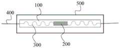
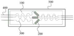
在本发明的一个方面,本发明提出了一种柔性石墨烯关节传感器。根据本发明的实施例,参考图1和2,该柔性石墨烯关节传感器包括:第一柔性层100、石墨烯传感单元200、可延展导线结构300、外接导线400和第二柔性层500。其中,第一柔性层100的一侧表面为第一表面;石墨烯传感单元200设在所述第一表面;可延展导线结构300包括基线层310和导电层320,基线层310形成在第一表面的至少部分表面,导电层320形成在基线层310远离第一表面的至少部分表面,可延展导线结构300与石墨烯传感单元200相连;外接导线400与可延展导线结构300中的导电层320相连;第二柔性层500的一侧表面为第二粘性表面,第二粘性表面与第一表面相对设置,并覆盖石墨烯传感单元200、可延展导线结构300、第一表面和部分外接导线400,第二粘性表面的面积大于第一表面的面积。In one aspect of the present invention, the present invention proposes a flexible graphene joint sensor. According to an embodiment of the present invention, referring to FIGS. 1 and 2 , the flexible graphene joint sensor includes: a first
下面进一步对根据本发明实施例的柔性石墨烯关节传感器进行详细描述。The flexible graphene joint sensor according to the embodiment of the present invention will be further described in detail below.
根据本发明的实施例,上述第一柔性层100和第二柔性层500的具体种类并不受特别限制,可以采用本领域常见的柔性材料,在本发明的一些实施例中,第一柔性层100的第一表面也为粘性表面,该粘性表面和第二柔性层500的第二粘性表面可以通过在本领域常见的柔性材料一侧施加本领域常见的粘结剂而获得。第一柔性层100和第二柔性层500均具有粘性表面,可以进一步提高产品的封装效果。According to the embodiments of the present invention, the specific types of the first
根据本发明的实施例,上述基线层310可以由聚酰亚胺(PI)形成,起到支持导电层320的作用。According to an embodiment of the present invention, the above-mentioned
根据本发明的实施例,上述导电层320包括铬层和金层,所述铬层与所述基线层310相连,所述金层形成在所述铬层远离所述基线层310的表面。导电层320包括下层铬层和上层金层,铬层与基线层310直接接触,由此,可以在保证导电层320导电能力的同时,进一步提高导电层320与基线层310附着力。According to an embodiment of the present invention, the
根据本发明的实施例,上述铬层的厚度可以为5~20nm(例如5nm、10nm、15nm、20nm等),上述金层的厚度可以为80~300nm(例如80nm、120nm、160nm、200nm、250nm、300nm等)。由此,可以进一步提高导电层320的导电能力以及导电层320与基线层310的附着力。According to an embodiment of the present invention, the thickness of the chromium layer may be 5-20 nm (eg 5 nm, 10 nm, 15 nm, 20 nm, etc.), and the thickness of the gold layer may be 80-300 nm (eg 80 nm, 120 nm, 160 nm, 200 nm, 250 nm) , 300nm, etc.). Thereby, the conductivity of the
根据本发明的实施例,上述外接导线400可以由异方性导电胶(ACF)、导电热压斑马纸或银形成。也即是说,外接导线400可以采用ACF线或导电热压斑马纸或银线。当外接导线400采用ACF线或导电热压斑马纸时,可通过热压法连接可延展导线结构300与ACF线或导电热压斑马纸;当外接导线400采用银线时,可采用银胶连接可延展导线结构300与ACF线。According to an embodiment of the present invention, the above-mentioned
根据本发明的实施例,上述石墨烯传感单元可以包括多个。由此,可以设置多个石墨烯传感单元组成应变花,以便获得更加丰富的应变信息。According to an embodiment of the present invention, the above-mentioned graphene sensing unit may include a plurality of units. Thus, multiple graphene sensing units can be set to form strain rosettes, so as to obtain more abundant strain information.
根据本发明的实施例,参考图3,上述石墨烯传感单元200可包括两个,两个所述石墨烯单元200形成二轴应变花。二轴应变花中,两个石墨烯传感单元200的夹角可以为90°等。According to an embodiment of the present invention, referring to FIG. 3 , the above-mentioned
根据本发明的实施例,参考图4,上述石墨烯传感单元200可包括三个,三个所述石墨烯单元200形成三轴应变花。三轴应变花中,三个石墨烯传感单元200的夹角可以为45°、60°等。利用三轴应变花可以由三个石墨烯传感单元200上的应变信息计算得到主应变的大小和方向。According to an embodiment of the present invention, referring to FIG. 4 , the above-mentioned
在本发明的另一方面,本发明提出了一种制备上述实施例的柔性石墨烯关节传感器的方法。根据本发明的实施例,该方法包括:In another aspect of the present invention, the present invention provides a method for preparing the flexible graphene joint sensor of the above embodiment. According to an embodiment of the present invention, the method includes:
(1)提供基底,在基底表面依次形成牺牲层、基线层和导电层,在导电层上设置具有预定图案的光刻胶掩膜版,刻蚀预定图案区域外的导电层,以便得到具有预定图案的导电层。(1) Provide a substrate, sequentially form a sacrificial layer, a baseline layer and a conductive layer on the surface of the substrate, set a photoresist mask with a predetermined pattern on the conductive layer, and etch the conductive layer outside the predetermined pattern area to obtain a predetermined pattern. patterned conductive layer.
根据本发明的实施例,上述基底的具体种类并不受特别限制,例如可以采用硅片等。在一些实施例中,基底使用前,可预先用丙酮、乙醇、去离子水对基底进行清洗。According to the embodiment of the present invention, the specific type of the above-mentioned substrate is not particularly limited, for example, a silicon wafer or the like can be used. In some embodiments, the substrate may be cleaned with acetone, ethanol, or deionized water before use.
根据本发明的实施例,上述牺牲层可以采用本领域常见的光刻胶形成,例如聚甲基丙烯酸甲酯(PMMA)。According to an embodiment of the present invention, the above-mentioned sacrificial layer may be formed by using a common photoresist in the art, such as polymethyl methacrylate (PMMA).
根据本发明的实施例,在施加光刻胶和基线层材料后,可以利用匀胶机将材料甩匀,再进行后续处理。According to the embodiment of the present invention, after applying the photoresist and the base layer material, the material can be uniformly shaken by a glue spinner, and then the subsequent processing can be performed.
根据本发明的实施例,在牺牲层形成后,可将所得产品加热至100~115℃保温5~10min,继续加热至150~155℃保温5~8min,继续加热至180~190℃保温10~15min,然后将所得产品冷却,以便使牺牲层固化,同时降低牺牲层内的应力。According to the embodiment of the present invention, after the sacrificial layer is formed, the obtained product can be heated to 100-115°C for 5-10 minutes, continue to be heated to 150-155°C for 5-8 minutes, and further heated to 180-190°C for 10-10 minutes. After 15 min, the resulting product was cooled in order to solidify the sacrificial layer while reducing the stress within the sacrificial layer.
根据本发明的实施例,在基线层形成后,可将所得产品加热至80~90℃保温10~15min,继续加热至120~130℃保温30~35min,继续加热至150~160℃保温30~35min,继续加热至200~210℃保温30~35min,继续加热至250~260℃保温30~40min,然后将所得产品冷却,以便使所述基线层固化,同时降低基线层内的应力。According to the embodiment of the present invention, after the formation of the baseline layer, the obtained product can be heated to 80-90° C. for 10-15 minutes, continue to be heated to 120-130° C. for 30-35 minutes, and continue to be heated to 150-160° C. for 30- 35min, continue to heat to 200-210°C for 30-35min, continue to heat to 250-260°C for 30-40min, and then cool the obtained product to solidify the baseline layer and reduce the stress in the baseline layer.
根据本发明的实施例,导电层可使用电子束蒸发设备在基线层上蒸镀导电层材料获得。According to an embodiment of the present invention, the conductive layer may be obtained by evaporating the conductive layer material on the base layer using electron beam evaporation equipment.
根据本发明的实施例,上述具有预定图案的光刻胶掩膜版可以按照以下方法制备得到:设计可延展导线结构图形的掩膜版,使用光刻显影方法,将掩膜版上的图形转移到光刻胶上,以便获得具有预定图案的光刻胶掩膜版。进而,使用湿法刻蚀方法刻蚀光刻胶掩膜版图形区域外的导电层,以便获得具有预定图案的导电层。According to an embodiment of the present invention, the above-mentioned photoresist mask with a predetermined pattern can be prepared according to the following method: designing a mask with an extensible wire structure pattern, using a photolithography development method, and transferring the pattern on the mask onto the photoresist in order to obtain a photoresist mask with a predetermined pattern. Further, the conductive layer outside the pattern area of the photoresist mask is etched using a wet etching method, so as to obtain a conductive layer having a predetermined pattern.
(2)提供柔性基底,将基线层和具有预定图案的导电层转印到柔性基底表面,并刻蚀未被具有预定图案的导电层覆盖部分的基线层,以便得到可延展导线结构。(2) Provide a flexible substrate, transfer the baseline layer and the conductive layer with a predetermined pattern to the surface of the flexible substrate, and etch the baseline layer not covered by the conductive layer with the predetermined pattern, so as to obtain a stretchable wire structure.
根据本发明的实施例,可以通过反应离子刻蚀方法刻蚀未被具有预定图案的导电层覆盖部分的基线层,所述反应离子刻蚀方法的工艺参数包括:氧气流量为15~30sccm,射频功率为100~150W,气压为10~30Pa。According to an embodiment of the present invention, the baseline layer that is not covered by the conductive layer having a predetermined pattern can be etched by reactive ion etching. The power is 100-150W, and the air pressure is 10-30Pa.
(3)在柔性基底表面的预留位置设置石墨烯传感单元,将可延展导线结构与石墨烯传感器和外接导线连接。(3) A graphene sensing unit is arranged at a reserved position on the surface of the flexible substrate, and the stretchable wire structure is connected with the graphene sensor and an external wire.
根据本发明的实施例,当外接导线采用ACF线或导电热压斑马纸时,可通过热压法连接可延展导线结构与ACF线或导电热压斑马纸;当外接导线采用银线时,可采用银胶连接可延展导线结构与ACF线。According to the embodiment of the present invention, when ACF wire or conductive hot-pressed zebra paper is used as the external wire, the stretchable wire structure can be connected with the ACF wire or conductive hot-pressed zebra paper by hot pressing; when the external wire is made of silver wire, it can be Silver glue is used to connect the stretchable wire structure to the ACF wire.
(4)将第二柔性层的第二粘性表面覆盖至石墨烯传感单元、可延展导线结构和部分外接导线得到柔性石墨烯关节传感器。(4) Covering the second viscous surface of the second flexible layer on the graphene sensing unit, the stretchable wire structure and part of the external wire to obtain a flexible graphene joint sensor.
这里,需要说明的是,在本发明的柔性石墨烯关节传感器中,第一柔性层的一侧表面可以为粘性表面或不为粘性表面。当第一柔性层的一侧表面不为粘性表面时,该第一柔性层可直接采用上述柔性基底,以便获得柔性石墨烯关节传感器产品。当第一柔性层的一侧表面为粘性表面时,可将上述柔性基底移除,并提供一具有粘性表面的柔性层作为第一柔性层,并将第一柔性层的粘性表面覆盖至第二粘性表面,得到柔性石墨烯关节传感器产品。Here, it should be noted that, in the flexible graphene joint sensor of the present invention, one side surface of the first flexible layer may be a sticky surface or a non-sticky surface. When one side surface of the first flexible layer is not a sticky surface, the first flexible layer can directly use the above-mentioned flexible substrate, so as to obtain a flexible graphene joint sensor product. When one side surface of the first flexible layer is an adhesive surface, the above-mentioned flexible substrate can be removed, and a flexible layer with an adhesive surface is provided as the first flexible layer, and the adhesive surface of the first flexible layer is covered to the second flexible layer. Adhesive surface to obtain flexible graphene joint sensor products.
下面参考具体实施例,对本发明进行描述,需要说明的是,这些实施例仅仅是描述性的,而不以任何方式限制本发明。The present invention will be described below with reference to specific embodiments. It should be noted that these embodiments are merely illustrative and do not limit the present invention in any way.
实施例1Example 1
(1)提供PMMA/Si Wafer底层基片。(1) Provide PMMA/Si Wafer bottom substrate.
(a)先把硅片用有机溶液清洗(先后使用丙酮溶液、乙醇溶液分别70摄氏度水浴10min后去离子水冲洗)。(a) First, clean the silicon wafer with an organic solution (use acetone solution and ethanol solution successively in a water bath at 70 degrees Celsius for 10 minutes, and then rinse with deionized water).
(b)在硅片上涂上PMMA,使用匀胶机将PMMA甩匀(转速:400转/秒,30秒+4500转/秒,30秒),固化后得到PMMA牺牲层。固化的具体工艺为:加热至110~115℃保温5-10min,继续加热至150~155℃保温5~8min,继续加热至180~190℃保温10~15min后,自然冷却50~60min至室温,以降低PMMA层内的应力。(b) Coating PMMA on the silicon wafer, using a glue spinner to spin the PMMA evenly (rotation speed: 400 rpm, 30 seconds + 4500 rpm, 30 seconds), and obtain a PMMA sacrificial layer after curing. The specific process of curing is as follows: heating to 110-115 ℃ for 5-10 minutes, continuing to heat to 150-155 ℃ for 5-8 minutes, continuing to heat to 180-190 ℃ and holding for 10-15 minutes, and naturally cooling to room temperature for 50-60 minutes, to reduce the stress in the PMMA layer.
(2)在PMMA/Si Wafer底层基片上形成基线层PI。(2) A baseline layer PI is formed on the PMMA/Si Wafer base substrate.
(c)在PMMA牺牲层上旋涂聚酰亚胺材料,使用匀胶机将PI甩匀(转速:400转/秒,30秒+4500转/秒,30秒),固化后得到聚酰亚胺层。所述固化的工艺为:加热至80~90℃保温10~15min,继续加热至120~130℃保温30~35min,继续加热至150~160℃保温30~35min,继续加热至200~210℃保温30~35min,继续加热至250~260℃保温30~40min,自然冷却40~60min以降低聚酰亚胺层内的应力。(c) Spin-coat polyimide material on the PMMA sacrificial layer, use a glue spinner to spin PI evenly (rotation speed: 400 rpm, 30 seconds+4500 rpm, 30 seconds), and obtain polyimide after curing Amine layer. The curing process is as follows: heating to 80-90°C for 10-15 minutes, continuing to heat to 120-130°C for 30-35 minutes, continuing to heat to 150-160°C for 30-35 minutes, and continuing to heat to 200-210°C for insulation For 30 to 35 minutes, continue heating to 250 to 260°C for 30 to 40 minutes, and naturally cool for 40 to 60 minutes to reduce the stress in the polyimide layer.
(3)在基线层PI上形成可延展导线结构的导电层。(3) Forming a conductive layer of an extensible wire structure on the base layer PI.
(d)使用电子束蒸发设备在上述器件表面蒸镀上铬/金层,其中,Cr位于下层,Au位于上层。(d) Evaporating a chromium/gold layer on the surface of the device by using electron beam evaporation equipment, wherein Cr is located in the lower layer and Au is located in the upper layer.
(e)设计可延展导线图形的掩模版,使用光刻显影方法,将掩模版上的图形转移到光刻胶上形成可延展导线的掩模图形。(e) Designing a reticle for extending the wire pattern, and using a photolithography developing method to transfer the pattern on the reticle to the photoresist to form a mask pattern for extending the wire.
(f)使用湿法刻蚀方法刻蚀光刻胶掩膜图形区域外的Cr/Au,去胶后,形成Cr/Au导线结构。(f) etching the Cr/Au outside the photoresist mask pattern area by using a wet etching method, and after removing the adhesive, a Cr/Au wire structure is formed.
(4)提供一柔性基底,将所述基线层与可延展导线的导电层转印至所述柔性基底上(如PDMS、水凝胶等)。(4) Provide a flexible substrate, and transfer the base layer and the conductive layer of the extensible wire onto the flexible substrate (eg, PDMS, hydrogel, etc.).
(5)使用反应离子刻蚀(RIE)方法,刻蚀未被可延展导线的导电层覆盖区域的PI(条件:氧气流量15~30sccm,射频功率100~150W,气压10~30Pa)。(5) Using the reactive ion etching (RIE) method, etch the PI in the area not covered by the conductive layer of the ductile wire (conditions: oxygen flow rate 15-30 sccm, radio frequency power 100-150 W, air pressure 10-30 Pa).
(6)将可延展导线位于柔性基底两侧的端口与外接导线相连。所述外接导线可为ACF线或或导电热压斑马纸或银线。若使用ACF线或导电热压斑马纸,用热压法连接可延展导线和ACF线或导电热压斑马纸;若使用银线,用银胶连接可延展导线和银线。(6) Connect the ports of the stretchable wires on both sides of the flexible substrate to the external wires. The external wire can be ACF wire or conductive hot-pressed zebra paper or silver wire. If using ACF wire or conductive heat-pressed zebra paper, connect the extensible wire and ACF wire or conductive heat-pressed zebra paper by thermocompression; if using silver wire, use silver glue to connect the extensible wire and silver wire.
(7)将石墨烯传感单元放置于柔性基底上的中心预留位置,使用银胶将其两端与可延展导线的导电层相连,使两者接通。(7) The graphene sensing unit is placed in the center reserved position on the flexible substrate, and silver glue is used to connect both ends of the graphene sensing unit to the conductive layer of the extensible wire, so that the two are connected.
(8)将柔性层(第二柔性层,可以为聚氨酯膜和丙烯酸粘结剂组成的敷料)完全覆盖并超过柔性基底的范围,第二柔性层面向柔性基底的一侧具有粘性,进而将可延展导线和石墨烯传感单元从柔性基底上粘起,然后,在第二柔性层有可延展导线和石墨烯传感单元的区域上再覆盖一层柔性层(第一柔性层),粘性面朝向上述区域,用以将上述区域封装,实现将可延展导线和石墨烯传感单元紧紧粘牢在两层柔性覆盖层之间。同时,由于第二柔性层的覆盖面积比第一柔性层大,因此可以将第二柔性层的粘性面朝向皮肤,实现将器件贴于关节表面。(8) The flexible layer (the second flexible layer, which can be a dressing composed of a polyurethane film and an acrylic adhesive) is completely covered and exceeds the range of the flexible substrate, and the side of the second flexible layer facing the flexible substrate is adhesive, and then the flexible layer can be The stretched wire and the graphene sensing unit are glued from the flexible substrate, and then a flexible layer (the first flexible layer) is covered on the area of the second flexible layer with the stretchable wire and the graphene sensing unit. Facing the above area, the above area is used to encapsulate the above area, so that the stretchable wire and the graphene sensing unit are tightly adhered between the two flexible covering layers. At the same time, since the covering area of the second flexible layer is larger than that of the first flexible layer, the adhesive surface of the second flexible layer can face the skin, so that the device can be attached to the joint surface.
在本说明书的描述中,参考术语“一个实施例”、“一些实施例”、“示例”、“具体示例”、或“一些示例”等的描述意指结合该实施例或示例描述的具体特征、结构、材料或者特点包含于本发明的至少一个实施例或示例中。在本说明书中,对上述术语的示意性表述不必须针对的是相同的实施例或示例。而且,描述的具体特征、结构、材料或者特点可以在任一个或多个实施例或示例中以合适的方式结合。此外,在不相互矛盾的情况下,本领域的技术人员可以将本说明书中描述的不同实施例或示例以及不同实施例或示例的特征进行结合和组合。In the description of this specification, description with reference to the terms "one embodiment," "some embodiments," "example," "specific example," or "some examples", etc., mean specific features described in connection with the embodiment or example , structure, material or feature is included in at least one embodiment or example of the present invention. In this specification, schematic representations of the above terms are not necessarily directed to the same embodiment or example. Furthermore, the particular features, structures, materials or characteristics described may be combined in any suitable manner in any one or more embodiments or examples. Furthermore, those skilled in the art may combine and combine the different embodiments or examples described in this specification, as well as the features of the different embodiments or examples, without conflicting each other.
尽管上面已经示出和描述了本发明的实施例,可以理解的是,上述实施例是示例性的,不能理解为对本发明的限制,本领域的普通技术人员在本发明的范围内可以对上述实施例进行变化、修改、替换和变型。Although the embodiments of the present invention have been shown and described above, it should be understood that the above-mentioned embodiments are exemplary and should not be construed as limiting the present invention. Embodiments are subject to variations, modifications, substitutions and variations.
Claims (10)
Translated fromChinesePriority Applications (1)
| Application Number | Priority Date | Filing Date | Title |
|---|---|---|---|
| CN202010036552.3ACN111232914A (en) | 2020-01-14 | 2020-01-14 | Flexible graphene joint sensor and preparation method thereof |
Applications Claiming Priority (1)
| Application Number | Priority Date | Filing Date | Title |
|---|---|---|---|
| CN202010036552.3ACN111232914A (en) | 2020-01-14 | 2020-01-14 | Flexible graphene joint sensor and preparation method thereof |
Publications (1)
| Publication Number | Publication Date |
|---|---|
| CN111232914Atrue CN111232914A (en) | 2020-06-05 |
Family
ID=70877793
Family Applications (1)
| Application Number | Title | Priority Date | Filing Date |
|---|---|---|---|
| CN202010036552.3APendingCN111232914A (en) | 2020-01-14 | 2020-01-14 | Flexible graphene joint sensor and preparation method thereof |
Country Status (1)
| Country | Link |
|---|---|
| CN (1) | CN111232914A (en) |
Cited By (1)
| Publication number | Priority date | Publication date | Assignee | Title |
|---|---|---|---|---|
| CN116626950A (en)* | 2023-06-13 | 2023-08-22 | 清华大学 | Flexible sensing display devices and wearable devices |
Citations (6)
| Publication number | Priority date | Publication date | Assignee | Title |
|---|---|---|---|---|
| US20060056161A1 (en)* | 2004-09-10 | 2006-03-16 | Samsung Electronics Co., Ltd. | Flexible device, flexible pressure sensor, and fabrication method thereof |
| US20120090408A1 (en)* | 2010-10-14 | 2012-04-19 | Industrial Technology Research Institute | Method for manufacturing piezoresistive material, piezoresistive composition and pressure sensor device |
| CN109171715A (en)* | 2018-09-20 | 2019-01-11 | 清华大学 | Use the wearable device of flexible extending electrode acquisition EEG signals |
| GB201903503D0 (en)* | 2019-03-14 | 2019-05-01 | Hive Robotics Ltd | A multilayered sensing apparatus and method of use |
| CN109875557A (en)* | 2019-02-03 | 2019-06-14 | 浙江荷清柔性电子技术有限公司 | Array micropin formula flexibility electromyographic electrode and preparation method thereof |
| KR20190112883A (en)* | 2018-03-26 | 2019-10-08 | 주식회사 필더세임 | Hand wearable device and manufacturing method of the same |
- 2020
- 2020-01-14CNCN202010036552.3Apatent/CN111232914A/enactivePending
Patent Citations (6)
| Publication number | Priority date | Publication date | Assignee | Title |
|---|---|---|---|---|
| US20060056161A1 (en)* | 2004-09-10 | 2006-03-16 | Samsung Electronics Co., Ltd. | Flexible device, flexible pressure sensor, and fabrication method thereof |
| US20120090408A1 (en)* | 2010-10-14 | 2012-04-19 | Industrial Technology Research Institute | Method for manufacturing piezoresistive material, piezoresistive composition and pressure sensor device |
| KR20190112883A (en)* | 2018-03-26 | 2019-10-08 | 주식회사 필더세임 | Hand wearable device and manufacturing method of the same |
| CN109171715A (en)* | 2018-09-20 | 2019-01-11 | 清华大学 | Use the wearable device of flexible extending electrode acquisition EEG signals |
| CN109875557A (en)* | 2019-02-03 | 2019-06-14 | 浙江荷清柔性电子技术有限公司 | Array micropin formula flexibility electromyographic electrode and preparation method thereof |
| GB201903503D0 (en)* | 2019-03-14 | 2019-05-01 | Hive Robotics Ltd | A multilayered sensing apparatus and method of use |
Cited By (1)
| Publication number | Priority date | Publication date | Assignee | Title |
|---|---|---|---|---|
| CN116626950A (en)* | 2023-06-13 | 2023-08-22 | 清华大学 | Flexible sensing display devices and wearable devices |
Similar Documents
| Publication | Publication Date | Title |
|---|---|---|
| CN110393507B (en) | Structural design of flexible extensible electronic device and manufacturing method thereof | |
| CN109520411B (en) | Pre-stretched graphene flexible strain sensor and preparation method thereof | |
| Liu et al. | Adhesion‐free thin‐film‐like curvature sensors integrated on flexible and wearable electronics for monitoring bending of joints and various body gestures | |
| JP6411423B2 (en) | Highly extendable electronic components | |
| US11864872B2 (en) | Vital signs monitor | |
| WO2019222969A1 (en) | Flexible pressure sensor based on hemispheric microstructure and fabrication method therefor | |
| AU2018102177A4 (en) | Flexible pressure sensor based on hemispheric microstructure and fabrication method therefor | |
| CN207976237U (en) | Pliable pressure sensor based on broached-tooth design | |
| CN109323784A (en) | A piezoresistive flexible tactile sensor with double-layer snap-on micro-bosses | |
| CN101534624B (en) | Radiator combination | |
| CN110701992B (en) | Method for manufacturing capacitive strain sensor by taking sandpaper surface microstructure as template | |
| WO2004095536A2 (en) | Stretchable and elastic interconnects | |
| CN111232914A (en) | Flexible graphene joint sensor and preparation method thereof | |
| JP2006332588A (en) | Capacitor electrode layer, method for producing capacitor electrode layer, unit sensor using the electrode layer, and tactile sensor using the unit sensor | |
| CN110840417A (en) | Flexible malleable temperature sensing device and method of making same | |
| CN113218296A (en) | Elastic strain sensor and preparation method thereof | |
| Wang et al. | Somatosensory Electro‐Thermal Actuator through the Laser‐Induced Graphene Technology | |
| CN117309008A (en) | Capacitive piezoelectric hybrid flexible multi-mode sensor and preparation method thereof | |
| JP2000340805A (en) | Electronic part and manufacture | |
| JPH0438402A (en) | Strain gauges and their manufacturing methods | |
| CN119779135A (en) | Flexible omnidirectional sensor based on silver nanowires and liquid metal electrodes and preparation method thereof | |
| WO2021204284A1 (en) | Miura-ori folding structure-based electrically conductive elastomer and application thereof | |
| TW201207964A (en) | Flexible micro-system and manufacturing method thereof | |
| KR101065280B1 (en) | Flexible device using carbon nanotube and manufacturing method | |
| CN117387740A (en) | An acoustic particle velocity sensor and its preparation method and detection method |
Legal Events
| Date | Code | Title | Description |
|---|---|---|---|
| PB01 | Publication | ||
| PB01 | Publication | ||
| SE01 | Entry into force of request for substantive examination | ||
| SE01 | Entry into force of request for substantive examination |