CN111198843B - File system writing acceleration method based on bus control on application processor chip - Google Patents
File system writing acceleration method based on bus control on application processor chipDownload PDFInfo
- Publication number
- CN111198843B CN111198843BCN201911319133.4ACN201911319133ACN111198843BCN 111198843 BCN111198843 BCN 111198843BCN 201911319133 ACN201911319133 ACN 201911319133ACN 111198843 BCN111198843 BCN 111198843B
- Authority
- CN
- China
- Prior art keywords
- file system
- data
- file
- page
- write
- Prior art date
- Legal status (The legal status is an assumption and is not a legal conclusion. Google has not performed a legal analysis and makes no representation as to the accuracy of the status listed.)
- Active
Links
Images


Classifications
- G—PHYSICS
- G06—COMPUTING OR CALCULATING; COUNTING
- G06F—ELECTRIC DIGITAL DATA PROCESSING
- G06F16/00—Information retrieval; Database structures therefor; File system structures therefor
- G06F16/10—File systems; File servers
- G06F16/11—File system administration, e.g. details of archiving or snapshots
- G06F16/113—Details of archiving
- G—PHYSICS
- G06—COMPUTING OR CALCULATING; COUNTING
- G06F—ELECTRIC DIGITAL DATA PROCESSING
- G06F16/00—Information retrieval; Database structures therefor; File system structures therefor
- G06F16/10—File systems; File servers
- G06F16/16—File or folder operations, e.g. details of user interfaces specifically adapted to file systems
- Y—GENERAL TAGGING OF NEW TECHNOLOGICAL DEVELOPMENTS; GENERAL TAGGING OF CROSS-SECTIONAL TECHNOLOGIES SPANNING OVER SEVERAL SECTIONS OF THE IPC; TECHNICAL SUBJECTS COVERED BY FORMER USPC CROSS-REFERENCE ART COLLECTIONS [XRACs] AND DIGESTS
- Y02—TECHNOLOGIES OR APPLICATIONS FOR MITIGATION OR ADAPTATION AGAINST CLIMATE CHANGE
- Y02D—CLIMATE CHANGE MITIGATION TECHNOLOGIES IN INFORMATION AND COMMUNICATION TECHNOLOGIES [ICT], I.E. INFORMATION AND COMMUNICATION TECHNOLOGIES AIMING AT THE REDUCTION OF THEIR OWN ENERGY USE
- Y02D10/00—Energy efficient computing, e.g. low power processors, power management or thermal management
Landscapes
- Engineering & Computer Science (AREA)
- Theoretical Computer Science (AREA)
- Data Mining & Analysis (AREA)
- Databases & Information Systems (AREA)
- Physics & Mathematics (AREA)
- General Engineering & Computer Science (AREA)
- General Physics & Mathematics (AREA)
- Human Computer Interaction (AREA)
- Advance Control (AREA)
- Information Retrieval, Db Structures And Fs Structures Therefor (AREA)
Abstract
Translated fromChinese
Description
Translated fromChinese技术领域technical field
本发明属于嵌入式系统软件领域,涉及一种基于应用处理器片上总线控制的文件系统写加速方法。The invention belongs to the field of embedded system software, and relates to a file system write acceleration method based on application processor on-chip bus control.
背景技术Background technique
嵌入式系统是一种为特定应用而设计的专用计算机系统,随着当今社会对嵌入式系统的广泛应用,嵌入式系统面临着应用场景复杂、数据处理任务繁重等挑战。嵌入式系统的一个典型的应用就是数据的采集存储,为了方便对数据的访问和查找变得容易,在系统软件层面普遍应用文件系统。Embedded system is a special-purpose computer system designed for specific applications. With the widespread application of embedded systems in today's society, embedded systems are facing challenges such as complex application scenarios and heavy data processing tasks. A typical application of embedded systems is data collection and storage. In order to facilitate data access and search, file systems are commonly used at the system software level.
文件系统作为一种存储和组织计算机数据的方法,在嵌入式系统软件中被广泛应用,嵌入式系统软件中的文件系统受限于处理器性能及片上资源的限制,通常会对软件系统多任务或进程的运行带来速度上的不利影响,特别是在一些对实时性要求较高的应用场景,如航空航天、汽车电子等设备,文件系统的存储性能将成为直接影响整个系统的关键要素。As a method of storing and organizing computer data, the file system is widely used in embedded system software. The file system in embedded system software is limited by the performance of the processor and on-chip resources. Or the operation of the process brings adverse effects on the speed, especially in some application scenarios with high real-time requirements, such as aerospace, automotive electronics and other equipment, the storage performance of the file system will become a key element that directly affects the entire system.
因此,面对复杂而大量的数据处理环境且对性能要求较高的场景下,文件系统的存储性能加速是嵌入式系统领域十分关注的问题。Therefore, in the face of a complex and massive data processing environment with high performance requirements, the storage performance acceleration of the file system is a matter of great concern in the embedded system field.
发明内容Contents of the invention
本发明的目的在于克服上述现有技术的缺点,提供了一种基于应用处理器片上总线控制的文件系统写加速方法,该方法能够加速文件系统的存储性能。The purpose of the present invention is to overcome the above-mentioned shortcomings of the prior art, and provide a file system write acceleration method based on application processor on-chip bus control, which can accelerate the storage performance of the file system.
为达到上述目的,本发明所述的基于应用处理器片上总线控制的文件系统写加速方法,该加快方法通过文件系统与FPGA协处理器协同完成,所述文件系统运行在主处理器中,文件系统包括open()函数接口、read()函数接口、write()函数接口及close()函数接口;存储器经FPGA协处理器与应用处理器片上总线相连,文件系统用于在写入文件过程中Page的Tags信息的生成;外设数据流实时保存至协处理器的缓冲区,协处理器通过片上总线监听,暂存片上总线捕获的Page,将缓冲区内的数据替换该Page数据区;In order to achieve the above object, the file system writing acceleration method based on the application processor on-chip bus control of the present invention, the acceleration method is completed through the cooperation of the file system and the FPGA coprocessor, the file system runs in the main processor, and the file system The system includes open() function interface, read() function interface, write() function interface and close() function interface; the memory is connected to the on-chip bus of the application processor through the FPGA coprocessor, and the file system is used in the process of writing files Generation of Tags information of the Page; the peripheral data stream is saved to the buffer of the coprocessor in real time, and the coprocessor monitors through the on-chip bus, temporarily stores the Page captured by the on-chip bus, and replaces the data in the buffer with the Page data area;
具体包括以下步骤:Specifically include the following steps:
1)应用处理器操作系统启动,文件系统初始化完成,协处理器接收应用处理器及文件系统启动完成信号后进入同步通信状态,等待文件系统的操作信号;1) The application processor operating system starts, the file system initialization is completed, the coprocessor enters the synchronous communication state after receiving the application processor and the file system startup completion signal, and waits for the operation signal of the file system;
2)调用文件系统的open()函数创建文件,获得文件句柄;2) Call the open() function of the file system to create a file and obtain a file handle;
3)调用文件系统的write()函数向文件中写入外设数据,文件系统按固定文件大小向存储器中写入数据,其中,单次写入按Page大小进行,写入过程中文件系统仅生成Page的Tags信息,驱动层将Page的Tags信息拷贝至控制器的缓冲区;当协处理器获得数据写开始信号时,则开始监听片上总线的数据;3) Call the write() function of the file system to write peripheral data into the file, and the file system writes data to the storage according to the fixed file size, wherein, a single write is performed according to the Page size, and the file system only Generate the Tags information of the Page, and the driver layer copies the Tags information of the Page to the buffer of the controller; when the coprocessor obtains the data write start signal, it starts to monitor the data of the on-chip bus;
4)协处理器获取片上总线Page并暂存,然后将外设数据缓冲区内的数据按固定大小替换Page数据区,并向存储器发送替换后的Page;4) The coprocessor obtains the on-chip bus Page and temporarily stores it, then replaces the Page data area with the data in the peripheral data buffer according to a fixed size, and sends the replaced Page to the memory;
5)当剩余写入文件大小小于等于0时,则文件写入结束,否则,则转至步骤3);5) When the remaining written file size is less than or equal to 0, the file writing ends, otherwise, go to step 3);
6)文件系统调用close()函数关闭该文件。6) The file system calls the close() function to close the file.
在文件系统中建立与存储器驱动层底层通信机制,标志上层应用写入存储器的内容类型;对文件系统的write()函数体前后建立调用开始信号及结束信号,驱动底层Page写函数通过该标志判断上层调用函数是否将写入文件数据,当确认此次操作为写入文件数据操作时,则向存储器的控制器缓冲区写入该页的Tags信号,启动写命令。Establish a communication mechanism with the bottom layer of the memory driver layer in the file system to mark the content type written by the upper layer application to the memory; establish a call start signal and an end signal before and after the write() function body of the file system, and drive the underlying Page write function to judge through the mark Whether the upper-layer call function will write file data, when it is confirmed that this operation is a file data write operation, then write the Tags signal of this page to the controller buffer of the memory, and start the write command.
在应用处理器与FPGA协处理器之间建立同步通信机制,所述同步通信机制用于同步文件系统与协处理器之间对Page的协同写入操作;当文件系统调用write()函数开始向文件写入数据,在write()函数接口调用前后分别触发开始信号及结束信号,当协处理器接收到开始信号时,则启动片上总线监听模式,对Page数据区进行操作;当协处理器接收到结束信号时,则退出监听模式,同时将存储器与处理器局部恢复总线直连。A synchronous communication mechanism is set up between the application processor and the FPGA coprocessor, and the synchronous communication mechanism is used to synchronize the collaborative write operation of the Page between the file system and the coprocessor; when the file system calls the write () function, it begins to The file writes data, triggers the start signal and the end signal before and after the write() function interface call, when the coprocessor receives the start signal, it starts the on-chip bus monitoring mode, and operates the Page data area; when the coprocessor receives When the end signal is reached, the monitoring mode is exited, and at the same time, the memory is directly connected to the local recovery bus of the processor.
文件系统的write()函数接口对Page进行第一阶段操作,具体的,生成Tags信息并填充控制器缓冲区对应的区段,控制器缓冲区数据区位置保留但不进行操作;然后协处理器对Page进行第二阶段操作,具体的,将外部数据流缓冲区按固定大小替换Page数据区。The write() function interface of the file system performs the first-stage operation on the Page, specifically, generates Tags information and fills the section corresponding to the controller buffer, and the position of the controller buffer data area is reserved but not operated; then the coprocessor Perform the second-stage operation on the Page, specifically, replace the Page data area with the external data stream buffer with a fixed size.
协处理器的运行状态分为初始状态、同步通信状态、时序监听状态及数据插入状态,在初始状态,存储器与应用处理器片上总线直连;在同步通信状态;应用处理器文件系统初始化完成;在时序监听状态,调用文件系统的write()函数接口准备向文件写入数据;在数据插入状态,将外部数据缓冲区按固定大小替换Page数据区,向存储器发送Page;协处理器的各状态之间的转化由应用处理器及协处理器事件状态控制。The running state of the coprocessor is divided into initial state, synchronous communication state, timing monitoring state and data insertion state. In the initial state, the memory is directly connected to the on-chip bus of the application processor; in the synchronous communication state, the file system initialization of the application processor is completed; In the timing monitoring state, call the write() function interface of the file system to prepare to write data to the file; in the data insertion state, replace the Page data area with the external data buffer according to a fixed size, and send the Page to the memory; each state of the coprocessor The transition between them is controlled by the application processor and coprocessor event state.
本发明具有以下有益效果:The present invention has the following beneficial effects:
本发明所述的基于应用处理器片上总线控制的文件系统写加速方法在具体操作时,在文件系统中建立应用接口层与存储器控制器驱动层的通信标识,底层通过该标识判断本次底层调用对Page的操作;同时在应用处理器与协处理器之间建立快速通信机制,文件系统只需生成及拷贝Tags数据到控制器缓冲区,协处理器监听片上总线时序,将实际数据替换到Page的数据区;本发明减少了原文件系统对外部数据进行保存时的数据流路径,实现了由外部数据直接存储到存储器的最短路径,大大减少了Load-Store机制的处理器对数据的多次复制,其中,文件系统只需负责文件的创建及每个将写入页的Tags信息,减轻了主处理器调用文件系统写接口的代码执行量,从而加快文件系统写入性能。The file system write acceleration method based on the on-chip bus control of the application processor described in the present invention, in specific operation, establishes the communication identification between the application interface layer and the memory controller driver layer in the file system, and the bottom layer judges the call of the bottom layer through the identification. Page operations; at the same time, a fast communication mechanism is established between the application processor and the coprocessor. The file system only needs to generate and copy the Tags data to the controller buffer, and the coprocessor monitors the on-chip bus timing and replaces the actual data into the Page. data area; the present invention reduces the data flow path when the original file system saves the external data, realizes the shortest path directly stored from the external data to the memory, and greatly reduces the processor of the Load-Store mechanism for multiple times of data In replication, the file system only needs to be responsible for the creation of files and the Tags information of each page to be written, which reduces the amount of code execution for the main processor to call the file system write interface, thereby speeding up the file system write performance.
附图说明Description of drawings
图1为实施例一中应用本发明前后文件系统数据流通路对比图;Fig. 1 is a comparison diagram of file system data flow path before and after applying the present invention in embodiment one;
图2为实施例一的系统硬件连接图;Fig. 2 is the system hardware connection diagram of embodiment one;
图3为Yaffs2文件系统处理的具体函数调用过程图;Fig. 3 is the specific function calling process figure that Yaffs2 file system handles;
图4为FPGA不同状态的转化关系图。Fig. 4 is a conversion relationship diagram of different states of FPGA.
具体实施方式Detailed ways
下面结合附图对本发明做进一步详细描述:The present invention is described in further detail below in conjunction with accompanying drawing:
本发明通过文件系统与FPGA协处理器协同完成,所述FPGA协处理器位于应用处理器存储控制器与存储器之间,用于监听片上总线的时序,同时外设采集数据汇集到该处理器的缓冲区;协处理器监听片上总线的Page写入时序,并将该数据进行多级缓存,同时将外设数据缓冲区中的数据替换到Page数据区,数据区的大小根据存储器和存储器控制器缓冲区适配的值进行确定;The present invention is completed through the cooperation of the file system and the FPGA coprocessor, the FPGA coprocessor is located between the storage controller of the application processor and the memory, and is used to monitor the timing of the on-chip bus, and at the same time, the data collected by peripherals is collected into the processor's Buffer; the coprocessor monitors the page write timing of the on-chip bus, and multi-level caches the data, and replaces the data in the peripheral data buffer to the Page data area. The size of the data area depends on the memory and memory controller. The value of buffer adaptation is determined;
应用处理器运行软件系统,包含文件系统,FPGA协处理器作为本发明中的硬件,共同完成文件系统的软硬件协同加速;The application processor runs the software system, including the file system, and the FPGA coprocessor, as the hardware in the present invention, jointly completes the software and hardware collaborative acceleration of the file system;
所述文件系统运行在主处理器中,文件系统包括open()函数接口、read()函数接口、write()函数接口及close()函数接口;存储器经FPGA协处理器与应用处理器片上总线相连,文件系统用于在写入文件过程中Page的Tags信息的生成;外设数据流实时保存至协处理器的缓冲区,协处理器通过片上总线监听,暂存片上总线捕获的Page,将缓冲区内的数据替换该Page数据区;具体的,本发明所述的基于应用处理器片上总线控制的文件系统写加速方法具体包括以下步骤:Described file system runs in main processor, and file system comprises open () function interface, read () function interface, write () function interface and close () function interface; Memory is through FPGA coprocessor and application processor on-chip bus The file system is used to generate the Tags information of the Page in the process of writing the file; the peripheral data stream is saved to the buffer of the coprocessor in real time, and the coprocessor monitors through the on-chip bus, temporarily stores the Page captured by the on-chip bus, and sends the The data in the buffer zone replaces this Page data area; Concretely, the file system writing speed-up method based on application processor on-chip bus control of the present invention specifically comprises the following steps:
1)应用处理器操作系统启动,文件系统初始化完成,协处理器接收应用处理器及文件系统启动完成信号后进入同步通信状态,等待文件系统的操作信号;1) The application processor operating system starts, the file system initialization is completed, the coprocessor enters the synchronous communication state after receiving the application processor and the file system startup completion signal, and waits for the operation signal of the file system;
2)调用文件系统的open()函数创建文件,获得文件句柄;2) Call the open() function of the file system to create a file and obtain a file handle;
3)调用文件系统的write()函数向文件中写入外设数据,文件系统按固定文件大小向存储器中写入数据,其中,单次写入按Page大小进行,写入过程中文件系统仅生成Page的Tags信息,驱动层将Page的Tags信息拷贝至控制器的缓冲区;当协处理器获得数据写开始信号时,则开始监听片上总线的数据;3) Call the write() function of the file system to write peripheral data into the file, and the file system writes data to the storage according to the fixed file size, wherein, a single write is performed according to the Page size, and the file system only Generate the Tags information of the Page, and the driver layer copies the Tags information of the Page to the buffer of the controller; when the coprocessor obtains the data write start signal, it starts to monitor the data of the on-chip bus;
4)协处理器获取片上总线Page并暂存,然后将外设数据缓冲区内的数据按固定大小替换Page数据区,并向存储器发送替换后的Page;4) The coprocessor acquires the on-chip bus Page and temporarily stores it, then replaces the Page data area with the data in the peripheral data buffer according to a fixed size, and sends the replaced Page to the memory;
5)当剩余写入文件大小小于等于0时,则文件写入结束,否则,则转至步骤3);5) When the remaining written file size is less than or equal to 0, the file writing ends, otherwise, go to step 3);
6)文件系统调用close()函数关闭该文件。6) The file system calls the close() function to close the file.
在文件系统中建立与存储器驱动层底层通信机制,标志上层应用写入存储器的内容类型;对文件系统的write()函数体前后建立调用开始信号及结束信号,驱动底层Page写函数通过该标志判断上层调用函数是否将写入文件数据,当确认此次操作为文件数据写入操作时,则向存储器的控制器缓冲区写入该页的Tags信号,启动写命令。Establish a communication mechanism with the bottom layer of the memory driver layer in the file system to mark the content type written by the upper layer application to the memory; establish a call start signal and an end signal before and after the write() function body of the file system, and drive the underlying Page write function to judge through the mark Whether the upper-layer call function will write file data, when it is confirmed that this operation is a file data write operation, then write the Tags signal of this page to the controller buffer of the memory, and start the write command.
其中,当该标志位为1时,表示基于本发明的函数接口被调用,当该标志位为0时,表示该函数未被调用;存储器控制器驱动通过该全局标志位判断应用层所调用的文件系统接口;当驱动层写存储器缓冲区函数判断全局标志位为1时,标识上层应用软件调用本发明所设计的函数接口,仅对存储器控制器缓冲区的Tags信息进行操作和拷贝;当驱动层写存储器缓冲区函数判断全局标志位为0时,表示上层应用软件调用原始文件系统函数接口,驱动层保持原有Page处理过程不变,即将文件系统传递的固定长度的数据拷贝到存储器控制器缓冲区的数据段,将文件系统生成的Tags信息拷贝到控制器缓冲区的Tags区。Wherein, when the flag bit is 1, it means that the function interface based on the present invention is called, and when the flag bit is 0, it means that the function is not called; the memory controller driver judges the function called by the application layer through the global flag bit File system interface; when the driver layer writes the memory buffer function to judge that the global flag bit is 1, the upper layer application software of the mark calls the function interface designed by the present invention, and only operates and copies the Tags information of the memory controller buffer; When the layer write memory buffer function judges that the global flag bit is 0, it means that the upper layer application software calls the original file system function interface, and the driver layer keeps the original Page processing process unchanged, that is, the fixed-length data transferred by the file system is copied to the memory controller The data segment of the buffer, which copies the Tags information generated by the file system to the Tags area of the controller buffer.
在应用处理器与FPGA协处理器之间建立同步通信机制,所述同步通信机制用于同步文件系统与协处理器之间对Page的协同写入操作;当文件系统调用write()函数开始向文件写入数据,在write()函数接口调用前后分别触发开始信号及结束信号,当协处理器接收到开始信号时,则启动片上总线监听模式,对Page数据区进行操作;当协处理器接收到结束信号时,则退出监听模式,同时将存储器与处理器片上总线恢复直连。A synchronous communication mechanism is set up between the application processor and the FPGA coprocessor, and the synchronous communication mechanism is used to synchronize the collaborative write operation of the Page between the file system and the coprocessor; when the file system calls the write () function, it begins to The file writes data, triggers the start signal and the end signal before and after the write() function interface call, when the coprocessor receives the start signal, it starts the on-chip bus monitoring mode, and operates the Page data area; when the coprocessor receives When the end signal is reached, the monitoring mode is exited, and the direct connection between the memory and the on-chip bus of the processor is restored at the same time.
文件系统的write()函数接口对Page进行第一阶段操作,具体的,生成Tags信息并填充控制器缓冲区对应的区段,控制器缓冲区数据区位置保留但不进行操作;然后协处理器对Page进行第二阶段操作,具体的,将外部数据流缓冲区按固定大小替换Page数据区。The write() function interface of the file system performs the first-stage operation on the Page, specifically, generates Tags information and fills the section corresponding to the controller buffer, and the position of the controller buffer data area is reserved but not operated; then the coprocessor Perform the second-stage operation on the Page, specifically, replace the Page data area with the external data stream buffer with a fixed size.
协处理器的运行状态分为初始状态、同步通信状态、时序监听状态及数据插入状态,在初始状态,存储器与应用处理器片上总线直连;在同步通信状态;应用处理器文件系统初始化完成;在时序监听状态,调用文件系统的write()函数接口准备向文件写入数据;在数据插入状态,将外部数据缓冲区按固定大小替换Page数据区,向存储器发送Page;协处理器的各状态之间的转化由应用处理器及协处理器事件状态控制。The running state of the coprocessor is divided into initial state, synchronous communication state, timing monitoring state and data insertion state. In the initial state, the memory is directly connected to the on-chip bus of the application processor; in the synchronous communication state, the file system initialization of the application processor is completed; In the timing monitoring state, call the write() function interface of the file system to prepare to write data to the file; in the data insertion state, replace the Page data area with the external data buffer according to a fixed size, and send the Page to the memory; each state of the coprocessor The transition between them is controlled by the application processor and coprocessor event state.
本发明保证文件系统原有应用软件调用接口不变,添加基于本发明的文件数据写入函数接口,并保持该函数接口参数一致,方便上层应用接口迁移,在应用本发明时,仅需替换原文件系统写数据API函数名。The present invention ensures that the calling interface of the original application software of the file system remains unchanged, adds the file data writing function interface based on the present invention, and keeps the parameters of the function interface consistent, so as to facilitate the migration of the upper layer application interface. When applying the present invention, it is only necessary to replace the original File system write data API function name.
本发明中应用处理器采用PowerPC处理器,协处理器使用FPGA,数据存储介质采用NAND Flash,NAND Flash与PowerPC处理器片上总线均与FPGA相连,文件系统采用Yaffs2;外设采集的数据汇集到FPGA中的FIFO,应用软件保存该数据流数据。Among the present invention, application processor adopts PowerPC processor, and coprocessor uses FPGA, and data storage medium adopts NAND Flash, and NAND Flash and PowerPC processor on-chip bus are all connected with FPGA, and file system adopts Yaffs2; In the FIFO, the application software saves the data stream data.
实施例一Embodiment one
搭建数据采集的嵌入式系统,该系统片上硬件资源为:32位PowerPC处理器、128MBDDR、8M NorFlash、2GB NAND Flash以及FPGA;其中FPGA作为协处理器,外部采集数据流首先暂存在FPGA中;系统软件采用Yaffs2文件系统,应用层构建数据采集函数,调用文件系统标准API将数据保存到NAND Flash。Build an embedded system for data acquisition. The on-chip hardware resources of the system are: 32-bit PowerPC processor, 128MBDDR, 8M NorFlash, 2GB NAND Flash, and FPGA; FPGA is used as a coprocessor, and the external data stream is temporarily stored in FPGA; the system The software adopts the Yaffs2 file system, and the application layer constructs the data collection function, and calls the standard API of the file system to save the data to NAND Flash.
本实施例选用NAND Flash大小为2GB,单个Page大小为2KB+64B,PowerPC中的Flash控制器缓冲区大小设置为2KB+64B,文件系统中对页操作的参数也设置为该值,将软硬件参数统一。This embodiment selects NAND Flash size as 2GB, and the single Page size is 2KB+64B, and the Flash controller buffer size in PowerPC is set to 2KB+64B, and the parameter of page operation in the file system is also set to this value, and software and hardware The parameters are unified.
图1为应用本发明前后文件系统数据流通路对比图。Fig. 1 is a comparison diagram of the data flow path of the file system before and after the application of the present invention.
原始数据流通路为:外部数据实时保存于FPGA中的异步FIFO,PowerPC处理器首先将FIFO中的数据拷贝到内存中开辟的连续空间Buffer区;文件系统初始化完成之后,将Buffer中的数据保存至文件,保存过程中将数据以Page为单位进行写入操作,对于每个Page,生成额外的OOB信息并附加到Tags区;将Page的数据区和OOB区分别填充到Flash控制器的缓存区,驱动层向该控制器发送写指令,完成单个Page的写入。The original data flow path is: the external data is stored in the asynchronous FIFO in the FPGA in real time, and the PowerPC processor first copies the data in the FIFO to the continuous space Buffer area opened in the memory; after the file system initialization is completed, the data in the Buffer is saved to File, during the saving process, the data is written in the unit of Page. For each Page, additional OOB information is generated and attached to the Tags area; the data area and OOB area of the Page are respectively filled into the buffer area of the Flash controller. The driver layer sends a write command to the controller to complete the writing of a single Page.
应用本发明后的数据通路为:外部数据保存至FPGA异步FIFO中,PowerPC处理器无需在内存开辟外部数据缓存区;Yaffs2文件系统负责创建文件,获取该文件句柄,在向该文件写入Page数据时,不对Flash控制器数据区进行操作,仅生数据该虚拟Page的OOB区数据并填充到控制器缓冲区,驱动层向控制器发送写指令;FPGA通过监听片上总线时序,将控制器向NAND Flash发送的Page时序进行二级暂存,并将FIFO中保存的外部数据按固定大小2KB替换到Page数据区。The data path after applying the present invention is: the external data is saved in the FPGA asynchronous FIFO, and the PowerPC processor does not need to open up the external data cache area in the memory; the Yaffs2 file system is responsible for creating the file, obtaining the file handle, and writing the Page data to the file When the flash controller data area is not operated, only the data in the OOB area of the virtual Page is generated and filled into the controller buffer, and the driver layer sends a write command to the controller; the FPGA sends the controller to the NAND by monitoring the on-chip bus timing. The Page timing sent by Flash is temporarily stored in the second level, and the external data stored in the FIFO is replaced to the Page data area with a fixed size of 2KB.
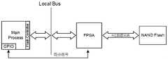
图2为系统硬件连接图。NAND Flash经FPGA连至PowerPC LocalBus,其数据总线长度为8位;PowerPC与FPGA之间通过2路GPIO进行通信,其中一路GPIO负责处理器启动完成同步信号,另一路GPIO作为文件系统Page写入过程开始同步信号。Figure 2 is the system hardware connection diagram. NAND Flash is connected to PowerPC LocalBus via FPGA, and its data bus length is 8 bits; PowerPC and FPGA communicate through 2 GPIOs, one of which is responsible for the synchronization signal of the processor startup and completion, and the other GPIO is used as the file system Page writing process Start sync signal.
图3为Yaffs2文件系统处理的具体函数调用过程图,数据的保存需分别调用三个文件系统API,分别为yaffs_open()、yaffs_write_fpga()和yaffs_close();yaffs_open()创建文件,包含文件名和权限属性等,并返回该文件句柄;yaffs_write_fpga()为应用本发明所实现的文件写入API,该接口与yaffs2标准API保持参数个数与类型的一致,使本发明的应用变得方便;yaffs_close()关闭该文件句柄,标志着一段数据保存到文件的过程完成。Figure 3 is the specific function call process diagram of the Yaffs2 file system processing. To save data, three file system APIs need to be called respectively, namely yaffs_open(), yaffs_write_fpga() and yaffs_close(); yaffs_open() creates a file, including the file name and permissions Attribute etc., and return this file handle; yaffs_write_fpga () writes API for the file realized by applying the present invention, this interface and yaffs2 standard API keep the consistency of parameter number and type, make the application of the present invention become convenient; yaffs_close( ) closes the file handle, marking the completion of the process of saving a piece of data to the file.
yaffs_open()和yaffs_write_fpga()在底层均调用Flash控制器缓冲区写操作,在yaffs2文件系统中,使用全局变量FPGA_FLAG供驱动层对缓冲区写操作的上层调用接口进行判断;当Flash控制器驱动层被yaffs_open()调用时,保持原驱动层对Page的操作不变;当Flash控制器驱动层被yaffs_write_fpga()调用时,驱动层写缓冲区函数只向缓冲区写入OOB信息,向Flash控制器发送写指令。Both yaffs_open() and yaffs_write_fpga() call the Flash controller buffer write operation at the bottom layer. In the yaffs2 file system, the global variable FPGA_FLAG is used for the driver layer to judge the upper layer call interface of the buffer write operation; when the Flash controller driver layer When called by yaffs_open(), the operation of the original driver layer on the Page remains unchanged; when the Flash controller driver layer is called by yaffs_write_fpga(), the driver layer write buffer function only writes OOB information to the buffer and writes to the Flash controller Send a write command.
参考图3,详细说明yaffs_write_fpga()函数处理过程。Referring to Fig. 3, the process of the yaffs_write_fpga() function is described in detail.
yaffs_open()函数在打开或创建文件之后返回句柄handle,该函数参数列表中,TestT为内存缓冲区指针,指向内存数据Buffer,nBytes为将要存入的字节数;yaffs_write_fpga()获取文件句柄指针和句柄对象,下层调用yaffs_WriteDataToFile()函数;yaffs_WriteDataToFile()函数内包含while循环,单个循环写一个Page,当剩余写入缓冲区数据长度小于0,循环结束,文件内容写入完成。The yaffs_open() function returns the handle handle after opening or creating a file. In the function parameter list, TestT is the memory buffer pointer, pointing to the memory data Buffer, and nBytes is the number of bytes to be stored; yaffs_write_fpga() obtains the file handle pointer and Handle object, the lower layer calls the yaffs_WriteDataToFile() function; the yaffs_WriteDataToFile() function contains a while loop, and a single loop writes a Page. When the length of the remaining write buffer data is less than 0, the loop ends and the file content is written.
yaffs2文件系统底层处理函数yaffs_WriteChunkDataToObject()到yaffs_WriteChunkWithTagsToNAND()函数依次为对写page的处理操作;MTD层nandmtd2_WriteChunkWithTagsToNAND()到fsl_elbc_write_buf()为NAND Flash控制器驱动层函数,完成软件层最终数据写入。The underlying processing functions of the yaffs2 file system, yaffs_WriteChunkDataToObject() to yaffs_WriteChunkWithTagsToNAND(), are the processing operations on the write page in turn; the MTD layer nandmtd2_WriteChunkWithTagsToNAND() to fsl_elbc_write_buf() are NAND Flash controller driver layer functions to complete the final data writing of the software layer.
Flash控制器缓冲区由fsl_elbc_write_buf()完成,当判断写入长度等于64时,表示本次调用写入OOB数据;否则继续判断FPGA_FLAG的值,当该值为true,操作为空,为false则写入data;当控制器缓冲区数据操作完成,向FCM发送写指令,FCM在硬件上启动写时序。The flash controller buffer is completed by fsl_elbc_write_buf(). When it is judged that the write length is equal to 64, it means that this call writes OOB data; otherwise, continue to judge the value of FPGA_FLAG. When the value is true, the operation is empty, and if it is false, write Enter data; when the controller buffer data operation is completed, it sends a write command to the FCM, and the FCM starts the write sequence on the hardware.
当yaffs_WriteDataToFile()函数的while循环判断还要继续写入的字节nByte小于等于0,表示文件系统写入数据完成,立即向FPGA发送写结束信号,同时将全局标志变量FPGA_FLAG赋值为false,FPAG接收到该信号退出时序监听状态。When the while loop of the yaffs_WriteDataToFile() function judges that the byte nByte to be written is less than or equal to 0, it means that the file system writes data is completed, and immediately sends a write end signal to the FPGA, and at the same time assigns the global flag variable FPGA_FLAG to false, and the FPGA receives When this signal exits the timing monitoring state.
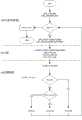
图4为FPGA不同状态的转化关系图,启动上电之后,PowerPC拉高GPIO1,FPGA接收到该信号后进入同步通信状态;在同步通信状态下,当FPGA捕获到GPIO2拉高信号,进入NAND Flash时序监听模式;当捕获到片上总线的Page后进入数据插入状态,将其进行二级寄存,将异步FIFO中的数据与Page数据区进行替换,结束后重回时序监听模式;当GPIO2拉低,表示该文件写入过程结束,返回同步通信状态。Figure 4 is the conversion relationship diagram of different states of FPGA. After the power is turned on, PowerPC pulls up GPIO1, and FPGA enters the synchronous communication state after receiving the signal; in the synchronous communication state, when FPGA captures the GPIO2 pull-up signal, it enters the NAND Flash Timing monitoring mode; when the Page on the on-chip bus is captured, it enters the data insertion state, registers it in the second level, replaces the data in the asynchronous FIFO with the Page data area, and returns to the timing monitoring mode after the end; when GPIO2 is pulled low, Indicates that the file writing process is over and returns to the synchronous communication state.
以上所述仅为本发明的一种实施方式,不是全部或唯一的实施方式,本领域普通技术人员通过阅读本发明说明书而对本发明技术方案采取的任何等效的变换,均为本发明权利要求所涵盖。The above is only one embodiment of the present invention, not all or the only embodiment, and any equivalent transformation taken by those of ordinary skill in the art to the technical solution of the present invention by reading the description of the present invention is a claim of the present invention covered.
Claims (5)
Priority Applications (1)
| Application Number | Priority Date | Filing Date | Title |
|---|---|---|---|
| CN201911319133.4ACN111198843B (en) | 2019-12-19 | 2019-12-19 | File system writing acceleration method based on bus control on application processor chip |
Applications Claiming Priority (1)
| Application Number | Priority Date | Filing Date | Title |
|---|---|---|---|
| CN201911319133.4ACN111198843B (en) | 2019-12-19 | 2019-12-19 | File system writing acceleration method based on bus control on application processor chip |
Publications (2)
| Publication Number | Publication Date |
|---|---|
| CN111198843A CN111198843A (en) | 2020-05-26 |
| CN111198843Btrue CN111198843B (en) | 2023-03-28 |
Family
ID=70744403
Family Applications (1)
| Application Number | Title | Priority Date | Filing Date |
|---|---|---|---|
| CN201911319133.4AActiveCN111198843B (en) | 2019-12-19 | 2019-12-19 | File system writing acceleration method based on bus control on application processor chip |
Country Status (1)
| Country | Link |
|---|---|
| CN (1) | CN111198843B (en) |
Families Citing this family (2)
| Publication number | Priority date | Publication date | Assignee | Title |
|---|---|---|---|---|
| CN112001494A (en) | 2020-08-20 | 2020-11-27 | 浪潮电子信息产业股份有限公司 | Method for realizing support of FPGA (field programmable Gate array) back-end equipment by nGraph framework |
| CN113253942B (en)* | 2021-06-25 | 2022-12-20 | 深圳小米通讯技术有限公司 | File writing method and its device, file reading method and its device, device and medium |
Citations (3)
| Publication number | Priority date | Publication date | Assignee | Title |
|---|---|---|---|---|
| WO2017020647A1 (en)* | 2015-08-04 | 2017-02-09 | 深圳市中兴微电子技术有限公司 | Novel storage-based embedded file system and realization method thereof |
| CN106909441A (en)* | 2017-02-28 | 2017-06-30 | 焦点科技股份有限公司 | The method that a kind of direct I/O of disk based on JVM is accessed |
| CN109683818A (en)* | 2018-12-17 | 2019-04-26 | 联想(北京)有限公司 | A kind of date storage method, equipment and storage medium |
Family Cites Families (2)
| Publication number | Priority date | Publication date | Assignee | Title |
|---|---|---|---|---|
| US20060294312A1 (en)* | 2004-05-27 | 2006-12-28 | Silverbrook Research Pty Ltd | Generation sequences |
| KR102343642B1 (en)* | 2014-07-24 | 2021-12-28 | 삼성전자주식회사 | Method and Electronic Device for operating data |
- 2019
- 2019-12-19CNCN201911319133.4Apatent/CN111198843B/enactiveActive
Patent Citations (3)
| Publication number | Priority date | Publication date | Assignee | Title |
|---|---|---|---|---|
| WO2017020647A1 (en)* | 2015-08-04 | 2017-02-09 | 深圳市中兴微电子技术有限公司 | Novel storage-based embedded file system and realization method thereof |
| CN106909441A (en)* | 2017-02-28 | 2017-06-30 | 焦点科技股份有限公司 | The method that a kind of direct I/O of disk based on JVM is accessed |
| CN109683818A (en)* | 2018-12-17 | 2019-04-26 | 联想(北京)有限公司 | A kind of date storage method, equipment and storage medium |
Non-Patent Citations (1)
| Title |
|---|
| NAND存储器在嵌入式系统中的应用;高文青等;《电测与仪表》;20080225(第02期);全文* |
Also Published As
| Publication number | Publication date |
|---|---|
| CN111198843A (en) | 2020-05-26 |
Similar Documents
| Publication | Publication Date | Title |
|---|---|---|
| CN103250141B (en) | Networking client-server architecture structure in pre-read process | |
| JP4698599B2 (en) | Real time inking | |
| CN100555257C (en) | The memory controller of the dma operation between the processing page replicative phase and method | |
| CN109815029B (en) | Method for realizing communication between partitions of embedded partition operating system | |
| TWI321419B (en) | Atomic message division | |
| US7773090B1 (en) | Kernel mode graphics driver for dual-core computer system | |
| KR100881597B1 (en) | Read request processing system and method | |
| CN101261729B (en) | System and method for managing multiple threads in a distributed graphics processing unit | |
| JP6734768B2 (en) | System, device and method including storage device for performing dual write | |
| CN108932170A (en) | A Mechanism for Efficiently Shared Memory File System Between Co-resident Virtual Machines | |
| CN111198843B (en) | File system writing acceleration method based on bus control on application processor chip | |
| CN109147091B (en) | Unmanned vehicle data processing method, device, equipment and storage medium | |
| US10649686B2 (en) | Memory cache pressure reduction for pointer rings | |
| CN109710185A (en) | Data processing method and device | |
| CN104160397A (en) | Location independent files | |
| CN113821487B (en) | Local file system implementation method, device, equipment and storage medium | |
| CN104731569A (en) | Data processing method and relevant equipment | |
| CN113342836A (en) | Synchronous data processing method and device, computer equipment and storage medium | |
| CN114296646A (en) | IO service-based caching method, device, server and storage medium | |
| EP4538882A1 (en) | Data writing method and apparatus, data reading method and apparatus, electronic device, and storage medium | |
| CN115495020A (en) | File processing method and device, electronic equipment and readable storage medium | |
| TWI813001B (en) | Accelerating method of executing comparison functions and accelerating system of executing comparison functions | |
| JP3848268B2 (en) | Computer system, computer apparatus, data access method and program in computer system | |
| CN108304144A (en) | Data writing-in and reading method and system, and data reading-writing system | |
| CN112711925A (en) | Method for designing virtualization EMIF bus DSP software |
Legal Events
| Date | Code | Title | Description |
|---|---|---|---|
| PB01 | Publication | ||
| PB01 | Publication | ||
| SE01 | Entry into force of request for substantive examination | ||
| SE01 | Entry into force of request for substantive examination | ||
| GR01 | Patent grant | ||
| GR01 | Patent grant |