CN111192829B - Groove type VDMOS device and manufacturing method thereof - Google Patents
Groove type VDMOS device and manufacturing method thereofDownload PDFInfo
- Publication number
- CN111192829B CN111192829BCN201910468719.0ACN201910468719ACN111192829BCN 111192829 BCN111192829 BCN 111192829BCN 201910468719 ACN201910468719 ACN 201910468719ACN 111192829 BCN111192829 BCN 111192829B
- Authority
- CN
- China
- Prior art keywords
- trench
- mask
- type
- layer
- epitaxial layer
- Prior art date
- Legal status (The legal status is an assumption and is not a legal conclusion. Google has not performed a legal analysis and makes no representation as to the accuracy of the status listed.)
- Active
Links
- 238000004519manufacturing processMethods0.000titleclaimsabstractdescription47
- 229910021420polycrystalline siliconInorganic materials0.000claimsabstractdescription59
- 238000000034methodMethods0.000claimsabstractdescription52
- 210000000746body regionAnatomy0.000claimsabstractdescription51
- 238000002955isolationMethods0.000claimsabstractdescription27
- 238000005530etchingMethods0.000claimsabstractdescription23
- 229910052751metalInorganic materials0.000claimsabstractdescription20
- 239000002184metalSubstances0.000claimsabstractdescription20
- 238000000151depositionMethods0.000claimsabstractdescription18
- 230000008021depositionEffects0.000claimsabstractdescription8
- 229920005591polysiliconPolymers0.000claimsdescription57
- 238000002513implantationMethods0.000claimsdescription33
- 125000006850spacer groupChemical group0.000claimsdescription26
- 238000001039wet etchingMethods0.000claimsdescription21
- HQVNEWCFYHHQES-UHFFFAOYSA-Nsilicon nitrideChemical compoundN12[Si]34N5[Si]62N3[Si]51N64HQVNEWCFYHHQES-UHFFFAOYSA-N0.000claimsdescription17
- VYPSYNLAJGMNEJ-UHFFFAOYSA-NSilicium dioxideChemical groupO=[Si]=OVYPSYNLAJGMNEJ-UHFFFAOYSA-N0.000claimsdescription16
- 239000000758substrateSubstances0.000claimsdescription16
- 229910052581Si3N4Inorganic materials0.000claimsdescription14
- 230000000903blocking effectEffects0.000claimsdescription13
- 239000000463materialSubstances0.000claimsdescription12
- 238000012545processingMethods0.000claimsdescription12
- 229910052814silicon oxideInorganic materials0.000claimsdescription8
- 230000003647oxidationEffects0.000claimsdescription7
- 238000007254oxidation reactionMethods0.000claimsdescription7
- QVGXLLKOCUKJST-UHFFFAOYSA-Natomic oxygenChemical compound[O]QVGXLLKOCUKJST-UHFFFAOYSA-N0.000claimsdescription5
- 229910052760oxygenInorganic materials0.000claimsdescription5
- 239000001301oxygenSubstances0.000claimsdescription5
- 235000012239silicon dioxideNutrition0.000claimsdescription4
- 239000000377silicon dioxideSubstances0.000claimsdescription4
- TWNQGVIAIRXVLR-UHFFFAOYSA-Noxo(oxoalumanyloxy)alumaneChemical compoundO=[Al]O[Al]=OTWNQGVIAIRXVLR-UHFFFAOYSA-N0.000claimsdescription3
- 238000010586diagramMethods0.000description22
- 238000000206photolithographyMethods0.000description10
- 230000000694effectsEffects0.000description4
- 239000004065semiconductorSubstances0.000description4
- 229910052710siliconInorganic materials0.000description4
- 239000010703siliconSubstances0.000description4
- 238000012360testing methodMethods0.000description4
- ZOXJGFHDIHLPTG-UHFFFAOYSA-NBoronChemical compound[B]ZOXJGFHDIHLPTG-UHFFFAOYSA-N0.000description3
- 101100102849Saccharomyces cerevisiae (strain ATCC 204508 / S288c) VTH1 geneProteins0.000description3
- 230000009286beneficial effectEffects0.000description3
- 229910052796boronInorganic materials0.000description3
- 238000011056performance testMethods0.000description3
- 239000000243solutionSubstances0.000description3
- 230000003321amplificationEffects0.000description2
- 230000015572biosynthetic processEffects0.000description2
- 238000011065in-situ storageMethods0.000description2
- 238000003199nucleic acid amplification methodMethods0.000description2
- 230000003071parasitic effectEffects0.000description2
- 230000000717retained effectEffects0.000description2
- 229920006395saturated elastomerPolymers0.000description2
- 229910004298SiO 2Inorganic materials0.000description1
- XUIMIQQOPSSXEZ-UHFFFAOYSA-NSiliconChemical compound[Si]XUIMIQQOPSSXEZ-UHFFFAOYSA-N0.000description1
- 230000015556catabolic processEffects0.000description1
- 238000006243chemical reactionMethods0.000description1
- 238000009792diffusion processMethods0.000description1
- 238000001312dry etchingMethods0.000description1
- 230000005669field effectEffects0.000description1
- 239000012535impuritySubstances0.000description1
- 238000002347injectionMethods0.000description1
- 239000007924injectionSubstances0.000description1
- 238000005468ion implantationMethods0.000description1
- 238000005259measurementMethods0.000description1
- 229910044991metal oxideInorganic materials0.000description1
- 150000004706metal oxidesChemical class0.000description1
- 238000012986modificationMethods0.000description1
- 230000004048modificationEffects0.000description1
- 238000002360preparation methodMethods0.000description1
Images


Classifications
- H—ELECTRICITY
- H10—SEMICONDUCTOR DEVICES; ELECTRIC SOLID-STATE DEVICES NOT OTHERWISE PROVIDED FOR
- H10D—INORGANIC ELECTRIC SEMICONDUCTOR DEVICES
- H10D30/00—Field-effect transistors [FET]
- H10D30/01—Manufacture or treatment
- H10D30/021—Manufacture or treatment of FETs having insulated gates [IGFET]
- H10D30/028—Manufacture or treatment of FETs having insulated gates [IGFET] of double-diffused metal oxide semiconductor [DMOS] FETs
- H10D30/0291—Manufacture or treatment of FETs having insulated gates [IGFET] of double-diffused metal oxide semiconductor [DMOS] FETs of vertical DMOS [VDMOS] FETs
- H10D30/0297—Manufacture or treatment of FETs having insulated gates [IGFET] of double-diffused metal oxide semiconductor [DMOS] FETs of vertical DMOS [VDMOS] FETs using recessing of the gate electrodes, e.g. to form trench gate electrodes
- H—ELECTRICITY
- H10—SEMICONDUCTOR DEVICES; ELECTRIC SOLID-STATE DEVICES NOT OTHERWISE PROVIDED FOR
- H10D—INORGANIC ELECTRIC SEMICONDUCTOR DEVICES
- H10D30/00—Field-effect transistors [FET]
- H10D30/60—Insulated-gate field-effect transistors [IGFET]
- H10D30/64—Double-diffused metal-oxide semiconductor [DMOS] FETs
- H10D30/66—Vertical DMOS [VDMOS] FETs
- H10D30/668—Vertical DMOS [VDMOS] FETs having trench gate electrodes, e.g. UMOS transistors
Landscapes
- Metal-Oxide And Bipolar Metal-Oxide Semiconductor Integrated Circuits (AREA)
Abstract
Description
Translated fromChinese技术领域technical field
本发明属于VDMOS器件技术领域,尤其涉及一种沟槽型VDMOS器件及其制造方法。The invention belongs to the technical field of VDMOS devices, and in particular relates to a trench type VDMOS device and a manufacturing method thereof.
背景技术Background technique
半导体功率器件是电力电子系统进行能量控制和转换的基本电子元器件,其可控特性决定了电力电子系统的效率、体积和重量。自从垂直导电双扩散新结构的半导体功率器件诞生以来,以期独特的高输入阻抗、低驱动功率、高开关速度、由于的频率特性和良好的热稳定性等,使得电力电子技术得到了迅速发展。垂直导电双扩散半导体功率器件的代表主要是沟槽型垂直双扩散金属-氧化物半导体场效应晶体管(简称VDMOS),其集合了双极晶体管和普通MOS器件的优点。Semiconductor power devices are the basic electronic components for energy control and conversion in power electronic systems, and their controllable characteristics determine the efficiency, volume and weight of power electronic systems. Since the birth of semiconductor power devices with a new structure of vertical conductive double diffusion, power electronics technology has developed rapidly with the unique high input impedance, low driving power, high switching speed, excellent frequency characteristics and good thermal stability. The representative of the vertical conductive double-diffused semiconductor power device is mainly the trench vertical double-diffused metal-oxide semiconductor field effect transistor (VDMOS for short), which combines the advantages of bipolar transistors and ordinary MOS devices.
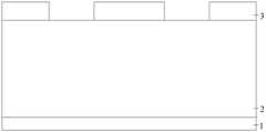
常规的沟槽型VDMOS器件的制造方法如下(具体参阅图1~11):The manufacturing method of the conventional trench type VDMOS device is as follows (refer to FIGS. 1-11 for details):
(1).在N型外延层2(N型外延层2与N型衬底1一体化)上方通过光刻刻蚀的方式形成带有开口的掩膜3,掩膜3的材料可以是氧化硅、氮化硅、氧化铝等,其厚度通常视沟槽的深度而定,通常情况下,沟槽深度越深,掩膜的厚度越厚,具体如图1、2所示;(1) A
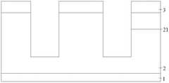
(2).在掩膜3的阻挡下,对N型外延层2进行第一沟槽21的刻蚀,具体如图3所示;(2). Under the blocking of the
(3).采用刻蚀工艺去除掩膜3,并在第一沟槽21内通过热氧化方法形成栅极氧化层4,之后填充原位掺杂的饱和N型多晶硅5,具体详见图4;(3) The
(4).对N型多晶硅5进行回刻处理,使得N型外延层2上表面的N型多晶硅5被去除,获得平坦的表面,N型多晶硅5的上表面与N型外延层2的上表面平齐,具体如图5所示;(4) Carry out etchback treatment on the N-
(5).在N型外延层2表面做体区6的注入和热驱入,形成体区6,具体如图6所示;(5). The
(6).在体区6上做源区的自对准注入和驱入,形成源区7,具体如图7所示;(6). Do self-aligned implantation and drive-in of the source region on the
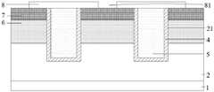
(7).在N型外延层2表面沉积介质层8,并完成接触孔81的刻蚀,具体如图8所示;(7). The
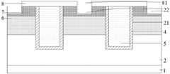
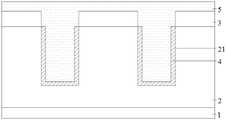
(8).自接触孔81底部对源区7进行刻蚀,使得源区7被刻穿,形成第二沟槽22,第二沟槽22主要是为了使得后续沉积的金属层与体区6有良好的短接效果,具体如图9所示;(8). The
(9).在外露的体区6、源区7、介质层8、栅极氧化层4及N型多晶硅5表面沉积金属层9,并在金属层9上形成源极引线,在N型多晶硅5表面形成栅极引线,在N型衬底1表面形成漏极引线,具体如图10所示。(9). Deposit a metal layer 9 on the surface of the exposed
上述制备方法在步骤(8)源区7的刻穿工艺中,由于源区7的结深通常为2000~3000埃,以及接触孔81过小、刻蚀的第二沟槽22间距过小,对于形成的第二沟槽22的深度很难进行测量和检查,无法保对证源区7刻穿时完全实现刻穿,于是在第二沟槽81的底部出现如图11所示的源区残留,源区残留会形成NP结,那么对具有源区残留的沟槽型VDMOS器件进行源漏间的二极管正向导通压降(Vfsd)测试时,Vfsd会全部失效,并且会寄生NPN三极管,在封装测试EAS时,会出现电流放大失控从而烧毁器件。In the above-mentioned preparation method, in the etching process of the
发明内容SUMMARY OF THE INVENTION
本发明的目的在于提供一种沟槽型VDMOS器件的制造方法,旨在解决常规沟槽型VDMOS器件制造方法由于源区残留而使得Vfsd测量全部失效且EAS测试会出现电流放大失控从而烧毁器件等问题。The purpose of the present invention is to provide a method for manufacturing a trench type VDMOS device, which aims to solve the problem that the conventional trench type VDMOS device manufacturing method causes the Vfsd measurement to fail completely due to the residual source region, and the EAS test will cause the current amplification to run out of control and burn out. device, etc.
进一步地,本发明还提供一种由上述方法获得的沟槽型VDMOS器件。Further, the present invention also provides a trench type VDMOS device obtained by the above method.
本发明是这样实现的:The present invention is realized in this way:
一种沟槽型VDMOS器件的制造方法,包括以下步骤:A manufacturing method of a trench type VDMOS device, comprising the following steps:
步骤S01.提供包括N型外延层的N型衬底;Step S01. Provide an N-type substrate including an N-type epitaxial layer;
步骤S02.在N型外延层表面进行掩膜处理,获得带有开口的掩膜;Step S02. Perform mask processing on the surface of the N-type epitaxial layer to obtain a mask with openings;
步骤S03.在所述掩膜的阻挡下,对N型外延层进行刻蚀处理,形成第一沟槽;Step S03. Under the blocking of the mask, the N-type epitaxial layer is etched to form a first trench;
步骤S04.在所述第一沟槽里生长栅极氧化层,并沉积N型多晶硅;Step S04. Grow a gate oxide layer in the first trench, and deposit N-type polysilicon;
步骤S05.对步骤S04获得的N型多晶硅进行回刻处理,使得N型多晶硅和所述掩膜齐平;Step S05. Perform etchback processing on the N-type polysilicon obtained in step S04, so that the N-type polysilicon and the mask are flush;
步骤S06.采用湿法工艺去除所述掩膜;Step S06. Use a wet process to remove the mask;
步骤S07.在所述N型外延层表面进行体区的自对准注入和驱入,形成器件体区,并在所述N型多晶硅侧壁形成掩膜侧墙;Step S07. Perform self-aligned implantation and drive-in of the body region on the surface of the N-type epitaxial layer to form a device body region, and form mask spacers on the N-type polysilicon sidewalls;
步骤S08.在所述掩膜侧墙的阻挡下,对所述N型外延层进行第二沟槽的刻蚀处理,形成第二沟槽;Step S08. Under the blocking of the mask sidewall, the N-type epitaxial layer is etched with a second trench to form a second trench;
步骤S09.在所述第二沟槽底部沉积形成一层隔离层;Step S09. depositing an isolation layer at the bottom of the second trench;
步骤S10.采用湿法腐蚀工艺去除所述掩膜侧墙,使得所述体区露出;Step S10. Use a wet etching process to remove the mask sidewall, so that the body region is exposed;
步骤S11.对露出的所述体区进行源区的注入和驱入,形成源区;Step S11. Perform source region implantation and drive-in to the exposed body region to form a source region;
步骤S12.采用湿法腐蚀工艺去除所述隔离层;Step S12. using a wet etching process to remove the isolation layer;
步骤S13.沉积形成介质层,并在介质层中刻蚀形成接触孔;Step S13. depositing to form a dielectric layer, and etching the dielectric layer to form contact holes;
步骤S14.沉积形成金属层并形成电极引线。Step S14. Deposition forming a metal layer and forming electrode leads.
以及,一种沟槽型VDMOS器件,该沟槽型VDMOS器件由如上的制造方法获得。And, a trench type VDMOS device obtained by the above manufacturing method.
本发明的有益效果如下:The beneficial effects of the present invention are as follows:
相对于现有技术,本发明提供的沟槽型VDMOS器件的制造方法,采用了新的制造工艺,不需要对源区进行刻穿,在金属层和体区接触部位不会存在源区残留,金属层和体区之间具有良好的短接效果,因此不会寄生出NPN三极管,同时还扩大了EAS和IMP的面积,使得获得的沟槽型VDMOS器件不仅具有极高的良品率,而且EAS也有大幅度提高、无Vfsd失效现象。Compared with the prior art, the manufacturing method of the trench type VDMOS device provided by the present invention adopts a new manufacturing process, does not need to pierce the source region, and there is no source region residue at the contact position between the metal layer and the body region, There is a good short-circuit effect between the metal layer and the body region, so the NPN transistor will not be parasitized, and the area of EAS and IMP is also enlarged, so that the obtained trench VDMOS device not only has a very high yield, but also EAS is also greatly improved without Vfsd failure.
本发明提供的沟槽型VDMOS器件,由于是采用上述的制造方法制造得到,其具有良好的EAS性能和Vfsd性能。The trench VDMOS device provided by the present invention has good EAS performance and Vfsd performance because it is manufactured by the above-mentioned manufacturing method.
附图说明Description of drawings
为了更清楚地说明本发明施例中的技术方案,下面将对实施例中所需要使用的附图作简单地介绍,显而易见地,下面描述中的附图仅仅是本发明的一些实施例,对于本领域普通技术人员来讲,在不付出创造性劳动的前提下,还可以根据这些附图获得其他的附图。In order to explain the technical solutions in the embodiments of the present invention more clearly, the following briefly introduces the accompanying drawings that need to be used in the embodiments. Obviously, the drawings in the following description are only some embodiments of the present invention. For those of ordinary skill in the art, other drawings can also be obtained from these drawings without any creative effort.
图1是常规沟槽型VDMOS器件的制造方法使用的N型外延层的示意图;1 is a schematic diagram of an N-type epitaxial layer used in a manufacturing method of a conventional trench type VDMOS device;
图2是常规沟槽型VDMOS器件的制造方法在N型外延层表面形成带有开口的掩膜的示意图;2 is a schematic diagram of forming a mask with an opening on the surface of an N-type epitaxial layer by a manufacturing method of a conventional trench type VDMOS device;
图3是常规沟槽型VDMOS器件的制造方法在N型外延层刻蚀形成沟槽的示意图;3 is a schematic diagram of a conventional trench-type VDMOS device manufacturing method forming a trench by etching an N-type epitaxial layer;
图4是常规沟槽型VDMOS器件的制造方法去除N型外延层掩膜后在沟槽上形成栅极氧化层、N型多晶硅的示意图;4 is a schematic diagram of forming a gate oxide layer and N-type polysilicon on the trenches after removing the N-type epitaxial layer mask by the manufacturing method of the conventional trench-type VDMOS device;
图5是常规沟槽型VDMOS器件的制造方法对N型多晶硅进行回刻形成平坦表面的示意图;5 is a schematic diagram illustrating that a conventional trench-type VDMOS device is manufactured by etching back N-type polysilicon to form a flat surface;
图6是常规沟槽型VDMOS器件的制造方法在N型外延层上进行注入和热驱入形成体区的示意图;Fig. 6 is the schematic diagram that the manufacturing method of the conventional trench type VDMOS device performs implantation and thermal drive-in to form the body region on the N-type epitaxial layer;
图7是常规沟槽型VDMOS器件的制造方法在体区上进行自对准注入和驱入形成源区的示意图;7 is a schematic diagram of self-aligned implantation and drive-in to form a source region on the body region of a conventional trench-type VDMOS device manufacturing method;
图8是常规沟槽型VDMOS器件的制造方法在N型外延层表面形成介质层并完成接触孔刻蚀的示意图;8 is a schematic diagram of forming a dielectric layer on the surface of the N-type epitaxial layer and completing the etching of the contact hole by a manufacturing method of a conventional trench type VDMOS device;
图9是常规沟槽型VDMOS器件的制造方法自接触孔向下对源区进行刻穿的示意图;Fig. 9 is the schematic diagram that the manufacturing method of the conventional trench type VDMOS device carries out the source region from the contact hole downwardly carved;
图10是常规沟槽型VDMOS器件的制造方法沉积形成金属层并形成电极引线的示意图;10 is a schematic diagram of depositing and forming a metal layer and forming electrode leads by a manufacturing method of a conventional trench type VDMOS device;
图11是常规沟槽型VDMOS器件的制造方法自接触孔向下对源区进行刻蚀无法实现彻底刻穿的示意图;11 is a schematic diagram showing that a conventional trench type VDMOS device manufacturing method etches the source region downward from the contact hole and cannot achieve complete engraving;
图12是本发明提供的沟槽型VDMOS器件的制造方法步骤S04中在第一沟槽上形成栅极氧化层、N型多晶硅的示意图;12 is a schematic diagram of forming a gate oxide layer and N-type polysilicon on the first trench in step S04 of the manufacturing method of the trench VDMOS device provided by the present invention;
图13是本发明提供的沟槽型VDMOS器件的制造方法步骤S05中对N型多晶硅进行回刻形成平坦表面的示意图;13 is a schematic diagram of performing back etching on N-type polysilicon to form a flat surface in step S05 of the manufacturing method of the trench VDMOS device provided by the present invention;
图14是本发明提供的沟槽型VDMOS器件的制造方法步骤S06中去除掩膜的示意图;14 is a schematic diagram of removing the mask in step S06 of the manufacturing method of the trench VDMOS device provided by the present invention;
图15是本发明提供的沟槽型VDMOS器件的制造方法步骤S07中自对准注入和驱入形成体区且在N型多晶硅侧壁形成掩膜侧墙的示意图;15 is a schematic diagram of self-aligned implantation and drive-in forming a body region and forming a mask spacer on the N-type polysilicon sidewall in step S07 of the manufacturing method of the trench VDMOS device provided by the present invention;
图16是本发明提供的沟槽型VDMOS器件的制造方法步骤S08中对N型外延层进行第二沟槽刻蚀的示意图;16 is a schematic diagram of performing second trench etching on the N-type epitaxial layer in step S08 of the manufacturing method of the trench VDMOS device provided by the present invention;
图17是本发明提供的沟槽型VDMOS器件的制造方法步骤S09中在第二沟槽上沉积形隔离层的示意图;17 is a schematic diagram of depositing a shape isolation layer on the second trench in step S09 of the manufacturing method of the trench type VDMOS device provided by the present invention;
图18是本发明提供的沟槽型VDMOS器件的制造方法步骤S10中去除掩膜侧墙的示意图;18 is a schematic diagram of removing the mask spacer in step S10 of the manufacturing method of the trench VDMOS device provided by the present invention;
图19是本发明提供的沟槽型VDMOS器件的制造方法步骤S11中在外露的体区上进行倾斜旋转注入和驱入形成源区的示意图;19 is a schematic diagram of performing tilt-rotation implantation and drive-in on the exposed body region to form a source region in step S11 of the manufacturing method of the trench VDMOS device provided by the present invention;
图20是本发明提供的沟槽型VDMOS器件的制造方法步骤S12中刻蚀去除隔离层的示意图;20 is a schematic diagram of etching and removing the isolation layer in step S12 of the manufacturing method of the trench VDMOS device provided by the present invention;
图21是本发明提供的沟槽型VDMOS器件的制造方法步骤S13中沉积介质层并形成接触孔的示意图;21 is a schematic diagram of depositing a dielectric layer and forming a contact hole in step S13 of the manufacturing method of the trench VDMOS device provided by the present invention;
图22是本发明提供的沟槽型VDMOS器件的制造方法步骤S14中金属层并形成电极引线的示意图;22 is a schematic diagram of the metal layer and the formation of electrode leads in step S14 of the manufacturing method of the trench VDMOS device provided by the present invention;
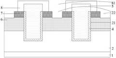
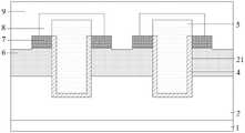
其中,1-N型衬底;2-N型外延层,21-第一沟槽,22-第二沟槽;3-掩膜(掩膜层);4-栅极氧化层;5-N型多晶硅;6-体区;7-源区;8-介质层,81-接触孔;9-金属层;10-掩膜侧墙;11-隔离层。Among them, 1-N type substrate; 2-N type epitaxial layer, 21-first trench, 22-second trench; 3-mask (mask layer); 4-gate oxide layer; 5-N 6-body region; 7-source region; 8-dielectric layer, 81-contact hole; 9-metal layer; 10-mask spacer; 11-isolation layer.
具体实施方式Detailed ways
为了使本发明要解决的技术问题、技术方案及有益效果更加清楚明白,以下结合实施例,对本发明进行进一步详细说明。应当理解,此处所描述的具体实施例仅仅用以解释本发明,并不用于限定本发明。In order to make the technical problems, technical solutions and beneficial effects to be solved by the present invention clearer, the present invention will be further described in detail below with reference to the embodiments. It should be understood that the specific embodiments described herein are only used to explain the present invention, but not to limit the present invention.
本发明一方面提供一种沟槽型VDMOS器件的制造方法。One aspect of the present invention provides a method for manufacturing a trench VDMOS device.
请参阅图1~3、12~22,该沟槽型VDMOS器件的制造方法包括以下步骤:Please refer to FIGS. 1 to 3 and 12 to 22. The manufacturing method of the trench VDMOS device includes the following steps:
步骤S01.提供包括N型外延层2的N型衬底1,参见图1;Step S01. Provide an N-
步骤S02.在N型外延层2表面进行掩膜处理,获得带有开口的掩膜3,参见图2;Step S02. Perform mask processing on the surface of the N-
步骤S03.在掩膜3的阻挡下,对N型外延层2进行刻蚀处理,形成第一沟槽21,参见图3;Step S03. Under the blocking of the
步骤S04.在第一沟槽21里生长栅极氧化层4,并沉积N型多晶硅5,参见图12;Step S04. Grow the
步骤S05.对步骤S04获得的N型多晶硅5进行回刻处理,使得N型多晶硅5和掩膜3齐平,参见图13;Step S05. Perform an etchback process on the N-
步骤S06.采用湿法工艺去除掩膜3,使得N型多晶硅5相对于N型外延层2具有凸起,具体参见图14;Step S06. Use a wet process to remove the
步骤S07.在N型外延层2表面进行体区的自对准注入和驱入,形成器件体区6,并在N型多晶硅5的侧壁形成掩膜侧墙10,获得如图15所示的结构;Step S07. Perform self-aligned implantation and drive-in of the body region on the surface of the N-
步骤S08.在掩膜侧墙10的阻挡下,对N型外延层6进行第二沟槽22的刻蚀处理,形成第二沟槽22,获得如图16所示的结构;Step S08. Under the blocking of the
步骤S09.在第二沟槽22底部沉积形成一层隔离层11,获得如图17所示的结构;Step S09. A layer of isolation layer 11 is deposited at the bottom of the
步骤S10.采用湿法腐蚀工艺去除掩膜侧墙10,使得体区6露出,获得如图18所示的结构;Step S10. Use a wet etching process to remove the
步骤S11.在露出的体区6表面进行源区的注入和驱入,形成源区7,获得如图19所示的结构;Step S11. Perform implantation and drive-in of the source region on the surface of the exposed
步骤S12.采用湿法腐蚀工艺去除隔离层11,获得如图20所示的结构;Step S12. Use a wet etching process to remove the isolation layer 11 to obtain the structure shown in FIG. 20;
步骤S13.沉积形成介质层8,并在介质层8中刻蚀形成接触孔81,获得如图21所示的结构;Step S13. Deposition to form a
步骤S14.沉积形成金属层9并形成电极引线,获得如图22所示的器件结构。Step S14. Deposition and forming the metal layer 9 and forming the electrode leads to obtain the device structure as shown in FIG. 22 .
下面对上述制造方法做详细的解释说明:The above manufacturing method is explained in detail below:
本发明涉及的N型衬底1应当清洁干燥,并且其上的N型外延层2也应当清洁干燥,避免后续加工过程中因为残留杂质或者污渍而导致加工效果差、接触不良。N型衬底1的厚度可以在500μm左右,避免在加工过程中发生翘曲。N型外延层2为在N型衬底1形成的一层材料层,其厚度为7μm~10μm,如可以是7.5μm、8.0μm、8.5μm、9.0μm、9.5μm、10μm,还可以是7μm~10μm之内的任一厚度。The N-
步骤S02中,在N型外延层2表面进行掩膜处理,其主要目的是为了获得具有形状的掩膜3,掩膜3的作用是便于后续刻蚀处理获得第一沟槽21。In step S02 , mask processing is performed on the surface of the N-
为了使得后续可以有效地去除掩膜3,其材料不能与栅极氧化层4相同。优选地,掩膜3的材料选自氮化硅、氧化铝中的任一种。In order to effectively remove the
步骤S03中,第一沟槽21的刻蚀处理采用干法刻蚀Si机台进行刻蚀。In step S03, the etching process of the
步骤S04中,在第一沟槽21里生长栅极氧化层4,目的是在第一沟槽21的内壁、底部形成一层将栅极和体区、源区分隔开的膜层,形成栅极氧化层4的材料为干氧氧化形成的SiO2。优选地,栅极氧化层4的厚度可以是500A~1500A,如可以是550A、600A、650A、700A、750A、800A、850A、900A、950A、1000A、1050A、1100A、1200A、1250A、1300A、1350A、1400A、1450A、1500A中的任一种。In step S04, the
沉积N型多晶硅5的目的是为了获得栅极,因此N型多晶硅5填充于第一沟槽21中,并且与栅极氧化层4有良好的接触,沉积得到的N型多晶硅5应该将掩膜3完全覆盖,以确保经过后续处理可以形成完整的栅极。The purpose of depositing the N-
填充的N型多晶硅5是原位掺杂的饱和N型多晶硅。The filled N-
步骤S05中,对N型多晶硅5进行回刻处理,主要是使得N型多晶硅5的上表面和掩膜3的上表面齐平,以便于对掩膜3进行去除处理,回刻处理工艺为常规工艺。In step S05, the N-
步骤S06中,湿法刻蚀掩膜3其目的是去除掩膜3,使得N型多晶硅5相对于N型外延层2具有凸起,方便后续工艺的进行,采用湿法刻蚀不损伤栅极氧化层4以及N型多晶硅5。使用的湿法刻蚀为常规的工艺,在此不再展开赘述。In step S06, the purpose of wet etching the
步骤S07中,体区6的注入和驱入。在N型多晶硅5的侧壁形成掩膜侧墙10的过程是对步骤S06得到的产品表面进行掩膜的沉积,并回刻,仅保留N型多晶硅5侧壁附近的掩膜,由此形成围绕在N型多晶硅5侧壁的掩膜侧墙10。In step S07, the implantation and drive-in of the
优选地,掩膜侧墙10的材料为氮化硅,以氮化硅作为掩膜侧墙10的材料,有利于后续湿法去除氮化硅,杜绝对栅极氧化及N型外延层的损伤。Preferably, the material of the
步骤S08中,对N型外延层6进行第二沟槽22的刻蚀处理,其刻蚀得到的第二沟槽22的深度应大于后续形成的源区7的深度,该刻蚀处理的工艺为常规工艺,在此不再赘述。In step S08, the N-
优选地,第二沟槽22的深度在4000~6000埃之间,如可以是4050A、4500A、5000A、5500A、5550A、5600A、5650A、6000A等。Preferably, the depth of the
步骤S09中,在第二沟槽22的底部沉积一层隔离层11,主要目的是确保后续形成源区时,源区没有注入和驱入第二沟槽22底部,从而避免源区7和体区6不发生交叉残留,彻底杜绝了NPN二极管的寄生。In step S09, a layer of isolation layer 11 is deposited on the bottom of the
沉积隔离层11的过程是先沉积一层隔离层,在进行回刻,使得仅在第二沟槽22底部保留有隔离层11,而掩膜侧墙10及其他部位不存在隔离层11。The process of depositing the isolation layer 11 is to deposit an isolation layer first, and then perform etchback, so that the isolation layer 11 remains only at the bottom of the
优选地,隔离层11的材料为氧化硅或氮化硅。Preferably, the material of the isolation layer 11 is silicon oxide or silicon nitride.
步骤S10中,湿法腐蚀工艺去除掩膜侧墙10的目的是去除掩膜侧墙10,使得N型多晶硅5再次露出,方便后续源区的注入和驱入处理,采用湿法刻蚀不损伤N型多晶硅5且不损伤隔离层11、体区6。使用的湿法腐蚀工艺为常规的工艺,在此不再展开赘述。In step S10, the purpose of removing the
步骤S11中,源区7的注入和驱入为常规工艺,在此不再展开赘述。In step S11 , the implantation and drive-in of the
优选地,源区7的深度在2000~3000埃之间,如可以是2050A、2100A、2150A、2200A、2250A、2300A、2350A、2400A、2450A、2500A、2550A、2600A、2650A、2700A、2750A、2800A、2850A、2900A、2950A、3000A等。Preferably, the depth of the
步骤S12中,湿法腐蚀工艺去除隔离层11的目的是去除隔离层11,使得体区6再次露出,方便后续沉积金属层9时能够与体区6形成完好的短接效果。采用湿法腐蚀工艺,不损伤体区6及源区7。使用的湿法腐蚀工艺为常规的工艺,在此不再展开赘述。In step S12 , the purpose of removing the isolation layer 11 by the wet etching process is to remove the isolation layer 11 so that the
步骤S13中,形成介质层8是在步骤S12得到的产品表面沉积一层介质层8,并采用刻蚀方式进行刻蚀,形成接触孔81,通过接触孔81使体区6和源区7露出,便于进行金属层9的沉积处理。In step S13, the formation of the
步骤S14中,直接在接触孔81中及介质层8表面沉积形成金属层9,并形成栅极引线、源极引线、漏极引线,其中栅极引线自N型多晶硅5中引出,源极引线自源区7引出,漏极引线自N型衬底1引出。In step S14, a metal layer 9 is deposited directly in the
本发明的沟槽型VDMOS器件的制造方法,采用了新的制造工艺,不需要对源区进行刻穿,而且极大地扩展了工艺窗口,便于离子植入(IMP),保证金属层和体区的短接效果,因此不会寄生出NPN三极管,获得的沟槽型VDMOS器件的EAS(单脉冲雪崩击穿能量)有大幅度提高、无Vfsd(源漏间的二极管导通压降)失效现象,沟槽型VDMOS器件良品率极高。The manufacturing method of the trench type VDMOS device of the present invention adopts a new manufacturing process, does not need to pierce the source region, and greatly expands the process window, which is convenient for ion implantation (IMP), and ensures the metal layer and the body region. Therefore, the NPN transistor will not be parasitized, theEAS (single-pulse avalanche breakdown energy) of the obtained trench VDMOS device is greatly improved, and there is no Vfsd (diode conduction voltage drop between source and drain) Failure phenomenon, the yield rate of trench VDMOS devices is extremely high.
基于上述的制造方法,另一方面,本发明还提供一种沟槽型VDMOS器件。该沟槽型VDMOS器件采用上述的方法制造,其具有良好的EAS性能和Vfsd性能。Based on the above manufacturing method, on the other hand, the present invention also provides a trench type VDMOS device. The trench type VDMOS device is manufactured by the above-mentioned method, and has good EAS performance and Vfsd performance.
为了更好的说明本发明的技术方案,下面结合具体实施例进行说明。In order to better illustrate the technical solutions of the present invention, the following description is made with reference to specific embodiments.
实施例1Example 1
请参阅图1~3、12~22,本实施例1提供一种沟槽型VDMOS器件的制造方法,具体包括以下步骤:Please refer to FIGS. 1 to 3 and 12 to 22.
(1).提供包括N型外延层2的N型衬底1,其中N型衬底1的厚度为500nm,电阻率为0.002Ω/cm,N型外延层2的厚度为8μm,电阻率为1.25Ω/cm,具体详见图1。(1) Provide an N-
(2).在N型外延层2的表面用低压炉管沉积0.7μm的掩膜层3,经过光刻刻蚀处理,获得带开口的掩膜3,具体详见图2。(2) A
(3).在掩膜3的阻挡下,对N型外延层2进行刻蚀处理,形成第一沟槽21,第一沟槽21的深度为1.6μm,具体详见图3。(3) Under the blocking of the
(4).在第一沟槽21里通过干氧氧化生长栅极氧化层4,栅极氧化层的材料为二氧化硅,其厚度为800A,并沉积18000A的N型多晶硅5,具体详见图12。(4). The
(5).对获得的N型多晶硅5进行回刻处理,使得N型多晶硅5和掩膜3齐平,具体详见图13。(5). The obtained N-
(6).采用湿法工艺去除掩膜3,使得N型多晶硅5相对于N型外延层2具有凸起,具体详见图14。(6) The
(7).在所述N型外延层2表面进行体区的自对准硼注入,注入能量为65Kev,注入剂量为1.5E13;接着1100℃下驱入55min,形成器件体区6,之后在N型外延层2表面淀积4000A氮化硅,再回刻淀积氮化硅,使得氮化硅在所述N型多晶硅5的侧壁形成掩膜侧墙10,具体详见图15。(7) Carry out self-aligned boron implantation in the body region on the surface of the N-
(8).在掩膜侧墙10的阻挡下,对N型外延层2进行第二沟槽22的刻蚀处理,形成第二沟槽22,第二沟槽22的深度为5000A,具体详见图16。(8). Under the blocking of the
(9).在第二沟槽22的表面淀积一层氧化硅,厚度为3000A,之后通过光刻刻蚀的方式,使得氧化硅仅在第二沟槽22的底部保留,残留的二氧化硅作为隔离层11,具体详见图17。(9). A layer of silicon oxide is deposited on the surface of the
(10).采用湿法腐蚀工艺去除掩膜侧墙10,使得体区6露出,具体详见图18。(10). The
(11).在露出的体区6表面进行源区的注入,注入能量为70Kev,注入剂量为5.5E15,注入后在950℃下驱入30min,得到源区7,源区7的深度为2500A,具体详见图19。(11) The source region is implanted on the surface of the exposed
(12).采用湿法腐蚀工艺去除隔离层11,使得第二沟槽22底部的体区6露出,具体详见图20。(12) The isolation layer 11 is removed by a wet etching process, so that the
(13).在源区7的表面及N型多晶硅5的表面沉积形成介质层8,并对介质层8中进行刻蚀形成接触孔81,具体详见图21。(13). A
(14).在体区6的表面、源区7的表面、介质层8的表面沉积形成金属层9,并进行光刻刻蚀形成电极引线,具体详见图22。(14) Deposit a metal layer 9 on the surface of the
对上述得到的沟槽型VDMOS器件进行相应性能测试,具体测试结果如表1所示。Corresponding performance tests were performed on the trench VDMOS devices obtained above, and the specific test results are shown in Table 1.
表1实施例1得到的沟槽型VDMOS器件的性能数据Table 1 Performance data of trench VDMOS devices obtained in Example 1
实施例2Example 2
请参阅图1~3、12~22,本实施例2提供一种沟槽型VDMOS器件的制造方法,具体包括以下步骤:Please refer to FIGS. 1 to 3 and 12 to 22.
(1).提供包括N型外延层2的N型衬底1,其中N型衬底1的厚度为500nm,电阻率为0.003Ω/cm,N型外延层2的厚度为8.5μm,电阻率为2.0Ω/cm,具体详见图1。(1) Provide an N-
(2).在N型外延层2的表面用低压炉管沉积0.7μm的掩膜层3,经过光刻刻蚀处理,获得带开口的掩膜3,具体详见图2。(2) A
(3).在掩膜3的阻挡下,对N型外延层2进行刻蚀处理,形成第一沟槽21,第一沟槽21的深度为1.6μm,具体详见图3。(3) Under the blocking of the
(4).在第一沟槽21里通过干氧氧化生长栅极氧化层4,栅极氧化层的材料为二氧化硅,其厚度为1000A,并沉积18000A的N型多晶硅5,具体详见图12。(4). The
(5).对获得的N型多晶硅5进行回刻处理,使得N型多晶硅5和掩膜3齐平,具体详见图13。(5). The obtained N-
(6).采用湿法工艺去除掩膜3,使得N型多晶硅5相对于N型外延层2具有凸起,具体详见图14。(6) The
(7).在所述N型外延层2表面进行体区的自对准硼注入,注入能量为65Kev,注入剂量为1.5E13;接着1100℃下驱入55min,形成器件体区6,之后在N型外延层2表面淀积4000A氮化硅,再回刻淀积氮化硅,使得氮化硅在所述N型多晶硅5的侧壁形成掩膜侧墙10,具体详见图15。(7) Carry out self-aligned boron implantation in the body region on the surface of the N-
(8).在掩膜侧墙10的阻挡下,对N型外延层2进行第二沟槽22的刻蚀处理,形成第二沟槽22,第二沟槽22的深度为5000A,具体详见图16。(8). Under the blocking of the
(9).在第二沟槽22的表面淀积一层氧化硅,厚度为3000A,之后通过光刻刻蚀的方式,使得氧化硅仅在第二沟槽22的底部保留,残留的二氧化硅作为隔离层11,具体详见图17。(9). A layer of silicon oxide is deposited on the surface of the
(10).采用湿法腐蚀工艺去除掩膜侧墙10,使得体区6露出,具体详见图18。(10). The
(11).在露出的体区6表面进行源区的注入,注入能量为70Kev,注入剂量为5.5E15,注入后在950℃下驱入30min,得到源区7,厚度为3000A,具体详见图19。(11) The source region is implanted on the surface of the exposed
(12).采用湿法腐蚀工艺去除隔离层11,使得第二沟槽22底部的体区6露出,具体详见图20。(12) The isolation layer 11 is removed by a wet etching process, so that the
(13).在源区7的表面及N型多晶硅5的表面沉积形成介质层8,并对介质层8中进行刻蚀形成接触孔81,具体详见图21。(13). A
(14).在体区6的表面、源区7的表面、介质层8的表面沉积形成金属层9,并进行光刻刻蚀形成电极引线,具体详见图22。(14) Deposit a metal layer 9 on the surface of the
对上述得到的沟槽型VDMOS器件进行相应性能测试,具体测试结果如表2所示。Corresponding performance tests are carried out on the trench VDMOS devices obtained above, and the specific test results are shown in Table 2.
表2实施例2得到的沟槽型VDMOS器件的性能数据Table 2 Performance data of trench VDMOS devices obtained in Example 2
实施例3Example 3
请参阅图1~3、12~22,本实施例3提供一种沟槽型VDMOS器件的制造方法,具体包括以下步骤:Please refer to FIGS. 1 to 3 and 12 to 22.
(1).提供包括N型外延层2的N型衬底1,其中N型衬底1的厚度为500nm,电阻率为0.005Ω/cm,N型外延层2的厚度为10μm,电阻率为1.20Ω/cm,具体详见图1。(1) Provide an N-
(2).在N型外延层2的表面用低压炉管沉积0.7μm的掩膜层3,经过光刻刻蚀处理,获得带开口的掩膜3,具体详见图2。(2) A
(3).在掩膜3的阻挡下,对N型外延层2进行刻蚀处理,形成第一沟槽21,第一沟槽21的深度为1.6μm,具体详见图3。(3) Under the blocking of the
(4).在第一沟槽21里通过干氧氧化生长栅极氧化层4,栅极氧化层的材料为二氧化硅,其厚度为1200A,并沉积18000A的N型多晶硅5,具体详见图12。(4). The
(5).对获得的N型多晶硅5进行回刻处理,使得N型多晶硅5和掩膜3齐平,具体详见图13。(5). The obtained N-
(6).采用湿法工艺去除掩膜3,使得N型多晶硅5相对于N型外延层2具有凸起,具体详见图14。(6) The
(7).在所述N型外延层2表面进行体区的自对准硼注入,注入能量为65Kev,注入剂量为1.5E13;接着1100℃下驱入55min,形成器件体区6,之后在N型外延层2表面淀积4000A氮化硅,再回刻淀积氮化硅,使得氮化硅在所述N型多晶硅5的侧壁形成掩膜侧墙10,具体详见图15。(7) Carry out self-aligned boron implantation in the body region on the surface of the N-
(8).在掩膜侧墙10的阻挡下,对N型外延层2进行第二沟槽22的刻蚀处理,形成第二沟槽22,第二沟槽22的深度为4000A,具体详见图16。(8). Under the blocking of the
(9).在第二沟槽22的表面淀积一层氧化硅,厚度为3000A,之后通过光刻刻蚀的方式,使得氧化硅仅在第二沟槽22的底部保留,残留的二氧化硅作为隔离层11,具体详见图17。(9). A layer of silicon oxide is deposited on the surface of the
(10).采用湿法腐蚀工艺去除掩膜侧墙10,使得体区6露出,具体详见图18。(10) The
(11).在露出的体区6表面进行源区的注入,注入能量为70Kev,注入剂量为5.5E15,注入后在950℃下驱入30min,得到源区7,厚度为2000A,具体详见图19。(11). The source region is implanted on the surface of the exposed
(12).采用湿法腐蚀工艺去除隔离层11,使得第二沟槽22底部的体区6露出,具体详见图20。(12) The isolation layer 11 is removed by a wet etching process, so that the
(13).在源区7的表面及N型多晶硅5的表面沉积形成介质层8,并对介质层8中进行刻蚀形成接触孔81,具体详见图21。(13). A
(14).在体区6的表面、源区7的表面、介质层8的表面沉积形成金属层9,并进行光刻刻蚀形成电极引线,具体详见图22。(14) Deposit a metal layer 9 on the surface of the
对上述得到的沟槽型VDMOS器件进行相应性能测试,具体测试结果如表3所示。Corresponding performance tests are performed on the trench VDMOS devices obtained above, and the specific test results are shown in Table 3.
表3实施例3得到的沟槽型VDMOS器件的性能数据Table 3 Performance data of trench VDMOS devices obtained in Example 3
以上所述仅为本发明的较佳实施例而已,并不用以限制本发明,凡在本发明的精神和原则之内所作的任何修改、等同替换和改进等,均应包含在本发明的保护范围之内。The above descriptions are only preferred embodiments of the present invention and are not intended to limit the present invention. Any modifications, equivalent replacements and improvements made within the spirit and principles of the present invention shall be included in the protection of the present invention. within the range.
Claims (3)
Translated fromChinesePriority Applications (1)
| Application Number | Priority Date | Filing Date | Title |
|---|---|---|---|
| CN201910468719.0ACN111192829B (en) | 2019-05-31 | 2019-05-31 | Groove type VDMOS device and manufacturing method thereof |
Applications Claiming Priority (1)
| Application Number | Priority Date | Filing Date | Title |
|---|---|---|---|
| CN201910468719.0ACN111192829B (en) | 2019-05-31 | 2019-05-31 | Groove type VDMOS device and manufacturing method thereof |
Publications (2)
| Publication Number | Publication Date |
|---|---|
| CN111192829A CN111192829A (en) | 2020-05-22 |
| CN111192829Btrue CN111192829B (en) | 2022-07-19 |
Family
ID=70710706
Family Applications (1)
| Application Number | Title | Priority Date | Filing Date |
|---|---|---|---|
| CN201910468719.0AActiveCN111192829B (en) | 2019-05-31 | 2019-05-31 | Groove type VDMOS device and manufacturing method thereof |
Country Status (1)
| Country | Link |
|---|---|
| CN (1) | CN111192829B (en) |
Families Citing this family (2)
| Publication number | Priority date | Publication date | Assignee | Title |
|---|---|---|---|---|
| CN112103186B (en)* | 2020-09-22 | 2022-03-15 | 深圳市芯电元科技有限公司 | A process method for improving cell density of trench MOSFET and structure of trench MOSFET |
| CN117316992A (en)* | 2023-11-29 | 2023-12-29 | 深圳基本半导体有限公司 | Silicon carbide MOSFET device with double-gate structure and preparation method thereof |
Citations (4)
| Publication number | Priority date | Publication date | Assignee | Title |
|---|---|---|---|---|
| US6211018B1 (en)* | 1999-08-14 | 2001-04-03 | Electronics And Telecommunications Research Institute | Method for fabricating high density trench gate type power device |
| CN102074478A (en)* | 2009-11-24 | 2011-05-25 | 上海华虹Nec电子有限公司 | Manufacturing process method for trench MOS |
| CN104916686A (en)* | 2014-03-12 | 2015-09-16 | 北大方正集团有限公司 | VDMOS device and manufacturing method thereof |
| CN108054211A (en)* | 2017-12-21 | 2018-05-18 | 深圳市晶特智造科技有限公司 | Trench-type vertical double-diffused metal oxide transistor and manufacturing method thereof |
Family Cites Families (6)
| Publication number | Priority date | Publication date | Assignee | Title |
|---|---|---|---|---|
| JP4932088B2 (en)* | 2001-02-19 | 2012-05-16 | ルネサスエレクトロニクス株式会社 | Insulated gate type semiconductor device manufacturing method |
| US7405452B2 (en)* | 2004-02-02 | 2008-07-29 | Hamza Yilmaz | Semiconductor device containing dielectrically isolated PN junction for enhanced breakdown characteristics |
| US7109552B2 (en)* | 2004-11-01 | 2006-09-19 | Silicon-Based Technology, Corp. | Self-aligned trench DMOS transistor structure and its manufacturing methods |
| CN102956487B (en)* | 2011-08-23 | 2014-12-10 | 上海华虹宏力半导体制造有限公司 | Manufacture method of isolation type power transistor |
| CN103117225B (en)* | 2013-01-29 | 2017-01-25 | 中航(重庆)微电子有限公司 | Production method preventing body effect in trench power MOS (metal oxide semiconductor) transistors |
| TW201503366A (en)* | 2013-07-08 | 2015-01-16 | Anpec Electronics Corp | Ditch type power semiconductor component and manufacturing method thereof |
- 2019
- 2019-05-31CNCN201910468719.0Apatent/CN111192829B/enactiveActive
Patent Citations (4)
| Publication number | Priority date | Publication date | Assignee | Title |
|---|---|---|---|---|
| US6211018B1 (en)* | 1999-08-14 | 2001-04-03 | Electronics And Telecommunications Research Institute | Method for fabricating high density trench gate type power device |
| CN102074478A (en)* | 2009-11-24 | 2011-05-25 | 上海华虹Nec电子有限公司 | Manufacturing process method for trench MOS |
| CN104916686A (en)* | 2014-03-12 | 2015-09-16 | 北大方正集团有限公司 | VDMOS device and manufacturing method thereof |
| CN108054211A (en)* | 2017-12-21 | 2018-05-18 | 深圳市晶特智造科技有限公司 | Trench-type vertical double-diffused metal oxide transistor and manufacturing method thereof |
Also Published As
| Publication number | Publication date |
|---|---|
| CN111192829A (en) | 2020-05-22 |
Similar Documents
| Publication | Publication Date | Title |
|---|---|---|
| CN103456790B (en) | Vertical power mosfet and forming method thereof | |
| CN105762176B (en) | Silicon carbide MOSFET device and preparation method thereof | |
| CN114038751B (en) | Manufacturing method of shielding grid MOSFET device with upper and lower structures | |
| WO2022061768A1 (en) | Power device and manufacturing method therefor | |
| CN110473911B (en) | A SiC MOSFET device and its manufacturing method | |
| CN111192829B (en) | Groove type VDMOS device and manufacturing method thereof | |
| CN105655402B (en) | Low-voltage super-junction MOSFET terminal structure and manufacturing method thereof | |
| CN105161539A (en) | Silicon carbide MOSFET device and manufacturing method thereof | |
| CN206022371U (en) | Igbt (IGBT) | |
| CN103915334B (en) | The manufacture method of double level polysilicon bipolar transistor | |
| CN112103181A (en) | Novel high-reliability IGBT and manufacturing method thereof | |
| CN114582965B (en) | A low switching loss power device structure and its manufacturing method | |
| CN113540229B (en) | Semiconductor device and method for manufacturing the same | |
| CN116053139A (en) | A method for manufacturing a trench-type double-gate semiconductor device | |
| CN104008975A (en) | Manufacturing method of groove-type power MOS transistor | |
| JP3921764B2 (en) | Manufacturing method of semiconductor device | |
| CN114823841A (en) | Semiconductor structure and forming method thereof | |
| JP3663657B2 (en) | Manufacturing method of semiconductor device | |
| CN110718586B (en) | A Trench Insulated Gate Transistor Device Against Latch-Up Effect | |
| CN118969850B (en) | Semiconductor structure and forming method thereof | |
| CN110400847A (en) | Trench Gate MOS Structure and Fabrication Process with Thick Bottom Oxide Layer | |
| CN114613680B (en) | A method for manufacturing a shielded gate trench device | |
| CN111755335A (en) | Semiconductor structure and method of forming the same | |
| CN104637810A (en) | Method for manufacturing emitter region of transistor | |
| CN113299641B (en) | SiC MOS device capable of improving ESD protection loop backwash characteristic |
Legal Events
| Date | Code | Title | Description |
|---|---|---|---|
| PB01 | Publication | ||
| PB01 | Publication | ||
| SE01 | Entry into force of request for substantive examination | ||
| SE01 | Entry into force of request for substantive examination | ||
| GR01 | Patent grant | ||
| GR01 | Patent grant |