CN1111823C - Image processing device using segment weighting correction and processing method thereof - Google Patents
Image processing device using segment weighting correction and processing method thereofDownload PDFInfo
- Publication number
- CN1111823C CN1111823CCN 97105523CN97105523ACN1111823CCN 1111823 CCN1111823 CCN 1111823CCN 97105523CN97105523CN 97105523CN 97105523 ACN97105523 ACN 97105523ACN 1111823 CCN1111823 CCN 1111823C
- Authority
- CN
- China
- Prior art keywords
- signal
- analog
- weighted
- electrical signal
- reference signals
- Prior art date
- Legal status (The legal status is an assumption and is not a legal conclusion. Google has not performed a legal analysis and makes no representation as to the accuracy of the status listed.)
- Expired - Fee Related
Links
Images


Landscapes
- Transforming Light Signals Into Electric Signals (AREA)
- Image Processing (AREA)
Abstract
Description
Translated fromChinese本发明是有关于一种影像处理装置,特别是有关于一种利用分段加权校正以改善输出影像灰阶密度的影像处理装置,还有关于使用分段加权校正的影像处理方法。本发明除了使用在影像系统之外,特别适用于影像扫描器输出影像的灰阶密度的改善上。The present invention relates to an image processing device, in particular to an image processing device using segmented weighted correction to improve the gray scale density of an output image, and also to an image processing method using segmented weighted correction. In addition to being used in image systems, the present invention is especially suitable for improving the grayscale density of images output by image scanners.
传统的影像处理系统,是用以将影像由光学系统的反射、聚焦,经一光电转换器转换成一电气讯号,再由电子电路对此电气讯号做校正、调整、储存、显示或进一步处理之用。此种影像系统应用非常广泛,输入影像扫描器(imagescanner)、摄影机和传真机等现代化世界中常见的设备。这些设备彼此间虽然有差异,但是影像讯号撷取和模拟数的转换都在很多影像系统中被使用。The traditional image processing system is used to reflect and focus the image from the optical system, convert it into an electrical signal through a photoelectric converter, and then use the electronic circuit to correct, adjust, store, display or further process the electrical signal . Such imaging systems are used in a wide variety of applications, inputting devices commonly found in the modern world such as image scanners, video cameras, and fax machines. Although there are differences between these devices, video signal acquisition and analog-to-digital conversion are used in many video systems.
以传统技术的影像扫描器为例,其方块图如图1所示,由一呆变数时序产生器9、一光源10、一玻璃表面11、一反射镜12、一透镜组合13、一电荷耦合器(Charge Couple Device;CCD)14、一由固定直流增益电压放大器15所构成的前置处理装置、一模拟数字转换器(analogue-to-digital convertor)16和一后置处理装置17组成。其中呆变数时序产生器9的输出脉冲如图2所示。而且每个时间间隔是相等的。如图2中时间间隔23和时间间隔27的大小是相同的。传统技术的影像扫描器运作的方式是,光源10发射光线照设在其后面具有图形或文字的玻璃表面11,以等速度扫描玻璃表面11,并反射到反射镜12,再由此反射到透镜组合13上。经由透镜组合13聚焦到电荷耦合器14上,并由电荷耦合器14转换成一电器讯号。其转换方式是由呆变数时序产生器9送出如图2中的脉冲,而且脉冲31的前沿(front edge)20送入电荷耦合器14时,电荷耦合器14传出前一时间间隔所累积的电荷并开始储存电荷,直到脉冲25的前沿(frontedge)24送入电荷耦合器14时,电荷耦合器14开始把在位于前沿20和前沿24之间的时间间隔23所得的讯号电荷传出并又开始储存电荷,而此时所获得的电气讯号即可用于后续电路之处理。固定直流增益电压放大器15调整此电气讯号的直流增益,并且送到模数字转换器16。而模拟数字转换器上的REF+和REF-是用来取样的参考电位,若经过固定直流增益电压放大器15所处理过的讯号的电压低于REF-,则其输出讯号一律定为系统的最小值,此最小值是相关于系统的最小灰阶值。若高于REF+则输出讯号一律定为系统的最大值,此最大值是相关于系统的最大灰阶值。后置处理17以一γ函数所产生的γ对映表调整输出影像的对比,经此而获得一可用以输出或进一步处理的影像讯号。很明显的,若是REF+和REF-之间的范围太小,可以用来表现影像的灰阶范围将会变小,所以要增加输出影像的品质就必须要把REF+和REF-之间的范围变大。Taking the image scanner of traditional technology as an example, its block diagram is shown in Figure 1. It consists of a variable timing generator 9, a light source 10, a glass surface 11, a mirror 12, a lens combination 13, a charge-coupled Charge Couple Device (CCD) 14, a pre-processing device composed of a fixed DC gain voltage amplifier 15, an analog-to-digital converter (analogue-to-digital converter) 16 and a post-processing device 17. Wherein the output pulse of the variable timing generator 9 is shown in FIG. 2 . And each time interval is equal. As shown in FIG. 2, the
如图3A所示,电荷耦合器(charge coupled device)的输出特性曲线(outputcharacterisic)和运算放大器(operation amplifier)的转移曲线(transfercurve)是只有在一特定区间才是线性的,其余区间都是非线性的。就图3A而言,若元件是电荷耦合器,则其水平座标是代表光通量,而垂直座标则是输出电压。若元件是运算放大器,则其水平座标是代表输入电压,而垂直座标则是代表输出电压。在图3A中区段b是线性区,但是区段a和c都是非线性区。因为具有低光通量的像素(pixels)都落在区段a内,所以在区段a内的图素代表的是影像的暗部讯号。具有高光通量的像素(pixels)都落在区段c内,所以在区段c内的图素代表的是影像的亮部讯号。As shown in Figure 3A, the output characteristic curve of a charge coupled device and the transfer curve of an operational amplifier are linear only in a specific interval, and the rest of the intervals are nonlinear of. As far as FIG. 3A is concerned, if the device is a charge-coupled device, its horizontal coordinate represents the luminous flux, while the vertical coordinate represents the output voltage. If the component is an operational amplifier, its horizontal axis represents the input voltage, while its vertical axis represents the output voltage. Section b in FIG. 3A is a linear region, but sections a and c are both non-linear regions. Because the pixels with low luminous flux all fall in the segment a, the pixels in the segment a represent the dark signal of the image. The pixels with high luminous flux all fall in the segment c, so the pixels in the segment c represent the bright signal of the image.
系统的转移曲线图示于图3B中,它是将第3A图倒转所获得的。图3B的水平座标轴代表的是输入灰阶密度,而垂直座标轴所代表的是输出灰阶密度。由图3B中可以很明显地发现,若输入的影像是位于暗部或亮部,因为区段a和c并不是线性的,所以其输出影像的灰阶密度会产生失真。若是可以让区段b的范围扩大,或是说让原来非线性区的图素移到线性区的范围内,则其输出影像的品质将会更好。The transfer curve diagram for the system is shown in Figure 3B, obtained by inverting Figure 3A. The horizontal axis of FIG. 3B represents the input grayscale density, and the vertical axis represents the output grayscale density. It can be clearly found from FIG. 3B that if the input image is located in the dark part or the bright part, the grayscale density of the output image will be distorted because the segments a and c are not linear. If the range of section b can be expanded, or the pixels in the original non-linear area can be moved into the range of the linear area, the quality of the output image will be better.
鉴于上述发明背景中,传统的影像处理装置无法在低成本的要求下,增加系统的灰阶密度与位元数。本发明的主要目的就是在提供一种改良式的讯号处理装置,使用不同灰阶对应不同曝光时间以及不同模拟数字转换参考电位,用以有效提升系统的灰阶密度,减少系统非线性特性对系统所产生的失真,并以较低的成本提高输出影像的对比。In view of the above-mentioned background of the invention, the traditional image processing device cannot increase the grayscale density and the number of bits of the system under the requirement of low cost. The main purpose of the present invention is to provide an improved signal processing device, which uses different gray scales corresponding to different exposure times and different analog-to-digital conversion reference potentials to effectively increase the gray scale density of the system and reduce the impact of the nonlinear characteristics of the system on the system. The resulting distortion and improve the contrast of the output image at a lower cost.
所以本发明的首要目的就是提供一个影像系统,使其转换曲线具有更大的线性区段。为了要扩大影像系统的线性区段,在不变动原有的电荷耦合器和运算放大器的规格下,有一个比较简便的方法就是控制电荷耦合系统的曝光时间以及依据曝光时间来改变模拟数字转换器的参考电压,所以本发明针对影像中具有高光通量和低光通量的部分做处理。因为要针对高光通量和低光通量的部分影像做处理,所以本发明把依据曝光时间来设定模拟数字转换器的参考电压,故本发明中的参考电压的个数比已知技术中的参考电压的个数更多。Therefore, the primary object of the present invention is to provide a video system whose conversion curve has a larger linear section. In order to expand the linear section of the imaging system, without changing the specifications of the original charge-coupled device and operational amplifier, a relatively simple method is to control the exposure time of the charge-coupled system and change the analog-to-digital converter according to the exposure time The reference voltage, so the present invention deals with the parts with high luminous flux and low luminous flux in the image. Because the partial images of high luminous flux and low luminous flux are to be processed, the present invention sets the reference voltage of the analog-to-digital converter according to the exposure time, so the number of reference voltages in the present invention is more than the reference voltage in the known technology. The number of is more.
根据以上所述目的,本发明提供了一种新的影像处理装置。本发明包含一个可以产生不同时间间隔的脉冲的加权控制讯号源,以及一个被加权控制讯号源所控制,而且可以将一个影像讯号转换成具有不同曝光时间的多次加权讯号的前置处理装置。一个多次取样系统,用以将一个多次加权讯号转换为一个多次取样数字讯号。还包括多个参考电位,用以在模拟数字转换器将一个模拟讯号转换成数字讯号时,依据多次加权讯号源输出讯号的时间间隔,而使得相关于不同时间间隔的数字讯号可以依据不同的参考电位将其转换成数字讯号。According to the above objectives, the present invention provides a new image processing device. The invention includes a weighted control signal source that can generate pulses with different time intervals, and a pre-processing device that is controlled by the weighted control signal source and can convert an image signal into multiple weighted signals with different exposure times. A multi-sampling system for converting a multi-weighted signal into a multi-sampled digital signal. It also includes a plurality of reference potentials, which are used to output signals according to the time interval of multiple weighted signal sources when the analog-to-digital converter converts an analog signal into a digital signal, so that the digital signals related to different time intervals can be based on different The reference potential converts it into a digital signal.
在第一实施例中,前述的前置处理系统包含将影像讯号转换成为一个电气讯号的电荷耦合器(charge coupled device),以及一个调整前述电气讯号的直流电压增益的直流增益电压放大器。而直流增益电压放大器中包含有一个运算放大器(operation amplifier)。多次取样系统则包含一个取样系统,用与加权控制讯号源的输出讯号相关的参考输入讯号,作为将一个模拟讯号转变成数字讯号参考电位,除此之外亦包含一个加法器。In the first embodiment, the aforementioned pre-processing system includes a charge coupled device for converting an image signal into an electrical signal, and a DC gain voltage amplifier for adjusting the DC voltage gain of the aforementioned electrical signal. The DC gain voltage amplifier contains an operational amplifier (operation amplifier). A multi-sampling system includes a sampling system that uses a reference input signal relative to the output signal of a weighted control signal source as a reference potential for converting an analog signal into a digital signal, and also includes an adder.
特别的是本发明有两个实施的方法,也就是线分割和点分割。在线分割的方法上是使用多个模拟数字转换器,而且每个模拟数字转换器上都有参考输入讯号,以作为取样的参考电位,并作后面步骤在决定哪一个灰阶值的像素可以通过的依据。也包含多个遮罩系统,用以让部分的灰阶值的像素可以通过遮罩装置,而其依据就是参考输入讯号,也就是说不同曝光时间的讯号可以通过不同的遮罩装置。In particular, the present invention has two methods of implementation, namely line segmentation and point segmentation. The method of online segmentation is to use multiple analog-to-digital converters, and each analog-to-digital converter has a reference input signal as a reference potential for sampling, and the following steps are used to determine which pixel of the gray scale value can pass basis. It also includes multiple masking systems, which are used to allow some grayscale pixels to pass through the masking device, and the basis is the reference input signal, that is to say, signals with different exposure times can pass through different masking devices.
在点分割的方法上是使用一个模拟数字转换器,而且这个模拟数字转换器上有一组可改变的参考输入讯号,以作为取样的参考电位,并作为后面步骤在决定哪一个灰阶值的像素可以通过遮罩装置时的依据,而且输入参考讯号是随着加权控制讯号的周期而改变其大小的。另外还包含一个多工器(multiplexer),用以顺序地处理一串资料中的位元。也包含一个遮罩系统,用以让部分的灰阶值的像素可以通过遮罩装置,而其依据就是参考输入讯号。与前述点分割内容相似,不同曝光时间的讯号可以通过相关于不同输入参考讯号时的遮罩装置。In the dot division method, an analog-to-digital converter is used, and there is a set of variable reference input signals on this analog-to-digital converter, which are used as the reference potential for sampling and used as the pixel for determining which grayscale value in the subsequent steps The basis can pass through the masking device, and the input reference signal changes its size along with the cycle of the weighting control signal. It also includes a multiplexer (multiplexer) to sequentially process the bits in a string of data. It also includes a masking system, which is used to allow part of the pixels of the gray scale value to pass through the masking device, and its basis is the reference input signal. Similar to the aforementioned dot segmentation, signals with different exposure times can pass through masking devices corresponding to different input reference signals.
后置处理装置,包括一个γ(Gamma)对映表,用于将多重取样数字讯号依据特性曲线,转换到一个转换后的讯号,以使得输出影像更为平顺(smooth)。并包含一个加法器用以将不同曝光时间的讯号相加起来,以形成一完整的影像讯号。The post-processing device includes a γ (Gamma) mapping table, which is used to convert the multi-sampled digital signal into a converted signal according to the characteristic curve, so as to make the output image smoother. It also includes an adder for adding signals of different exposure times to form a complete image signal.
图1为一传统影像扫描器的系统方块图。FIG. 1 is a system block diagram of a conventional image scanner.
图2为一传统影像扫描器的控制讯号源的输出波形。FIG. 2 is an output waveform of a control signal source of a conventional image scanner.
图3A为一电荷耦合器(charge coupled device)的输出讯号波形。FIG. 3A is an output signal waveform of a charge coupled device.
图3B为一传统影像扫描器的输出输入转移特性曲线(input output transfercurve)线。FIG. 3B is an input output transfer curve of a conventional image scanner.
图4为本发明装置中,使用分段加权校正的影像扫描器的输出输入特性曲线,其中的线性区比已知技术的系统的线性区更为加大。FIG. 4 is an output-input characteristic curve of an image scanner using segment weighting correction in the device of the present invention, wherein the linear region is larger than that of the system in the prior art.
图5说明了本发明的第一实施例的影像扫描器的功能方块图,其结构是使用空间分割。因为在电荷耦合器(eharge coupled device)之前的元件与已知技术相同,且与已知技术并无不同,所以由电荷耦合器开始说明。FIG. 5 illustrates a functional block diagram of an image scanner according to a first embodiment of the present invention, the structure of which uses space division. Since the components before the charge coupled device (eharge coupled device) are the same as the known technology and are not different from the known technology, the description starts with the charge coupled device.
图6说明了本发明所用的加权控制讯号源的输出讯号。Fig. 6 illustrates the output signal of the weighted control signal source used in the present invention.
图7显示本发明的第一实施例的影像装置中,输出输入转移特性曲线图。FIG. 7 is a graph showing the output-to-input transfer characteristics of the imaging device according to the first embodiment of the present invention.
图8说明了本发明的第二实施例的影像扫描器的功能方块图,其结构是使用时间分割。因为在电荷耦合器(charge coupled device)之前的元件与已知技术相同,且与已知技术并无不同,所以由电荷耦合器开始说明。FIG. 8 illustrates a functional block diagram of an image scanner according to a second embodiment of the present invention, which is structured using time division. Since the components before the charge coupled device are the same as the known technology and are not different from the known technology, the description begins with the charge coupled device.
在一影像系统中,影像由像素(pixel)组成,结果每个像素具有较多的色阶(shade),则可以组成更多的颜色,所表现出来的影像也会更接近原影像,对比也会更好。换句话说,也就是输出影像的品质更好。根据上述所提及,为了改善输出影像的品质,增加影像扫描器的灰阶密度(density range)是很重要的,因为这样可以使得每一个像素具有更多的色阶。In an image system, an image is composed of pixels. As a result, each pixel has more shades, so more colors can be formed, and the displayed image will be closer to the original image, and the contrast will be lower. will be better. In other words, the quality of the output image is better. According to the above mentioned, in order to improve the quality of the output image, it is very important to increase the density range of the image scanner, because each pixel can have more color levels.
影响影像扫描器输出影像品质的重要因素如下所述:首先是系统和电荷耦合器的灰阶密度。若设系统的灰阶密度是D则系统的信噪比(Signal-to-NoiseRatio)∶(S/N)s,和电荷耦合器的讯噪比:(S/N)c,必须满足下列式子:[(N/S)s+(N/S)c]≤10-D。其次是影像讯号的位元数。设若影像讯号的位元数是8,则讯噪比是28/1=256,所以灰阶密度D是log256=2.4。很清楚的,影像位元数越多灰阶密度越大,也就是说可以用更多的色阶来组成输出的影像。然后是后置处理装置所使用的γ对映表。根据所得的输入讯号的影像特性,可以获得一特定γ值的γ函数所产生的γ对映表,用以调整输出影像的特性。The important factors that affect the output image quality of the image scanner are as follows: First, the grayscale density of the system and the charge coupler. If the grayscale density of the system is D, then the signal-to-noise ratio (Signal-to-NoiseRatio) of the system: (S/N)s , and the signal-to-noise ratio of the charge coupler: (S/N)c , must satisfy the following formula Sub: [(N/S)s +(N/S)c ]≤10-D . The second is the number of bits of the video signal. Assuming that the number of bits of the image signal is 8, the signal-to-noise ratio is 28 /1=256, so the gray scale density D is log256=2.4. Obviously, the more image bits, the greater the gray scale density, that is to say, more color scales can be used to compose the output image. Then there is the gamma map used by the post-processing device. According to the obtained image characteristics of the input signal, a gamma mapping table generated by a gamma function with a specific gamma value can be obtained to adjust the characteristics of the output image.
在传统技术中是使用单次取样,纵使是为了要增加影像讯号的位元数,而使用多次取样,但是系统的讯噪比和电荷耦合器讯噪比仍不一定会满足下式[(N/S)s+(N/S)c]≤10-D。所以为了要满足上式,电荷耦合器的讯噪比可藉由分开处理及增加暗部曝光时间而增加之使其符合上式。而且如众所周知的,在一张图片上同时具有很多种灰阶,由很深到很浅都有。当曝光时间一增长,包括所有的亮部和暗部都有更长的曝光时间,所以亮部就反射更多的光至电荷耦合器,将导致电荷耦合器饱和(saturation)而失真(distoration)。如上所述若将亮部及暗部分开,暗部增长曝光处理,将可解决以上问题,同时也因为分开处理,本发明得以对暗部增长曝光以增加其光通量,并对亮部减少曝光时间以减少其光通量,使得系统的输出输入转移特性曲线的非线性问题得到解决。In the traditional technology, a single sampling is used. Even if multiple sampling is used to increase the number of bits of the image signal, the signal-to-noise ratio of the system and the signal-to-noise ratio of the charge coupler still do not necessarily satisfy the following formula [( N/S)s + (N/S)c ]≤10-D . Therefore, in order to satisfy the above formula, the signal-to-noise ratio of the charge coupler can be increased by processing separately and increasing the exposure time of the dark part so that it meets the above formula. And as we all know, there are many kinds of gray scales on a picture at the same time, ranging from very deep to very light. When the exposure time increases, all the bright parts and dark parts have a longer exposure time, so the bright parts reflect more light to the charge coupler, which will cause saturation of the charge coupler and distortion. As mentioned above, if the bright part and the dark part are separated, the dark part will increase the exposure processing, and the above problems will be solved. At the same time, because of the separate processing, the present invention can increase the exposure of the dark part to increase its luminous flux, and reduce the exposure time of the bright part to reduce its luminous flux. The luminous flux makes the nonlinear problem of the output-input transfer characteristic curve of the system solved.
上述的原理可参考图3A,输入影像中的暗部的像素有较小的光通量,例如X,所以其输出是透过区段a的转移而输出。而输入影像中的亮部的像素较大的光通量,例如Y,所以其输出是透过区段C的转移而输出。因为系统的输出输入转移特性曲线中,区段a和c是非线性的,所以光通量位于区段a和c的像素在输出时,其灰阶密度会有失真。为了使光通量于区段a和c的像素可以透过线性区段b而转移到输出,本发明设法使这些像素的光通量改变到线性区的光通量范围内。很明显的若是光通量Y减少和X增加,使其位于P和Q之间,则这些像素将有线性的输出输入转移特性曲线,所以藉由分段加权校正可以使得系统的输出输入特性转移曲线的线性区扩大,其改变后系统的输出输入特性转移曲线如图4中所示。The above-mentioned principle can be referred to FIG. 3A , the pixel in the dark part of the input image has a smaller luminous flux, such as X, so its output is output through the transfer of the segment a. The pixels in the bright part of the input image have a larger luminous flux, such as Y, so the output is output through the transfer of the segment C. Because the sections a and c are nonlinear in the output-input transfer characteristic curve of the system, the grayscale density of the pixels whose luminous flux is located in the sections a and c will be distorted when outputting. In order that the luminous flux of the pixels in sections a and c can be transferred to the output through the linear section b, the invention seeks to change the luminous flux of these pixels within the luminous flux range of the linear section. It is obvious that if the luminous flux Y decreases and X increases so that it is located between P and Q, then these pixels will have a linear output-input transfer characteristic curve, so the output-input characteristic transfer curve of the system can be adjusted by segmented weighted correction. The linear region expands, and the output-input characteristic transfer curve of the system after the change is shown in Fig. 4 .
本发明的第一实施例中使用加权多次取样、分开处理、分段加权校正以及影像合成,处理影像以作为显示或储存之用,所以可以运用于摄影机、录影机、传真机和影像扫描器等。本发明应用于影像扫描器系统中的实施例,作为本发明装置的较佳实施例,并作一详细说明。如图5所示的系统方块图包含一加权控制讯号产生器501、一电荷耦合器(Charge Couple Device:CCD)508、一以直流电压增益放大器构成的前置处理系统515,一模拟数字转换器(analog-to-ditialconverter)525、根据电荷耦合器508的输出讯号的灰阶值来分离讯号的遮罩510,此遮罩510可以用模拟数字转换器525的输入参考讯号502和503产生的讯号以作为参考的灰阶值、一加法器535、一以硬件或软件实现的γ对映表、一模拟数字转换器530、一遮罩520、一以硬件或软化实现的γ对映表550以及一后置加法器555。The first embodiment of the present invention uses weighted multiple sampling, separate processing, subsection weighted correction, and image synthesis to process images for display or storage, so it can be used in cameras, video recorders, fax machines, and image scanners wait. The embodiment of the present invention applied to the image scanner system is used as a preferred embodiment of the device of the present invention, and a detailed description will be given. The system block diagram shown in Figure 5 includes a weighted
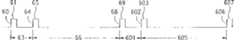
其中加权控制讯号产生器501的输出脉冲如图6所示,而时间间隔66是时间间隔63的10倍,而且时间间隔63和时间间隔601相同,时间间隔605和时间间隔606相同。The output pulse of the weighted
本发明应用于影像扫描器系统中的运作方式如下:光学影像被聚焦到电荷耦合器508上,并由电荷耦合器508转换成一电气讯号509。其转换方式是由时序产生器63送出如图6中的脉冲,而且脉冲61的前沿60送入电荷耦合器508时,电荷耦合器508将前一段时间所累积的电荷传出并且开始储存电荷,直到脉冲65的前沿64送入电荷耦合器508时,电荷耦合器508开始把在位于前沿60和前沿64之间的时间间隔63所得的讯号电荷传出并开始储存电荷,直到下一个脉冲抵达电荷耦合器。所以一个光学讯号被转换为一个电气讯号,而此时所获得的讯号即讯号509的亮部讯号。为了获得讯号509的暗部讯号,加权控制讯号产生器501的输出脉冲如图6所示,而时间间隔66是时间间隔63的10倍,也就是说电荷耦合器508的曝光时间在暗部是亮部的10倍,其方式是电荷耦合器508将时间间隔66所累积的电荷倒出来。The operation of the present invention in an image scanner system is as follows: an optical image is focused onto a
直流增益电压放大器515放大讯号509的直流电压以获得讯号511,模拟数字转换器525利用参考输入502和503作为参考电位,以将讯号511转换成一个数字讯号,并把这个数字讯号馈至遮罩510以获得讯号513。而讯号513即是将灰阶价值大于25.5的像素去掉。原因叙述于后段。然后加法器535处理讯号513以执行多次取样并产生暗部讯号536。暗部讯号536所包含的即是影像中的暗部的像素。而后置处理系统是由γ对应装置545和后置加法器555所组成,用以对暗部讯号的解析度做处理。而且γ对映表中的γ特性曲线的γ值大于1。The DC
在亮部讯号而言,讯号511经由模拟数字转换器530和遮罩520加法器540以执行多次取样,而产生一数字讯号,在本实施例中称为亮部讯号541。其中模拟数字转换器530使用参考输入504和505将讯号511转换为数字讯号,并将此数字讯号并馈至遮罩520以获得讯号521。后置处理系统是由γ对应装置550和后置加法器555所组成,用以对亮部讯号的解析度做处理。而且γ对应装置中的γ特性曲线的γ值小于1。For the highlight signal, the
暗部讯号536的对γ对应装置545输入后所产生的输出讯号暗部讯号546,而亮部讯号541的对γ对应装置550输入后所产生的输出讯号亮部讯号551。而暗部讯号546和亮部讯号551由加法器将两者相加以产生一个影像讯号,上面所述的加权控制讯号产生器510的输出图示于图6中,此时加权控制讯号产生器501可以用一般的计时脉冲产生器(如时序产生器9之属),将其输出以触发器(FlipFlop)或计数器(Counter)…等多项技术处理,即可获得不等时间间隔的脉冲输出。因此项技术为熟悉此项技术者所熟知,故未描述其结构。The output signal
在本发明的第一实施例当中,模拟数字转换器525利用参考输入502和503所提供的参考电位,用以转换讯号511成为一个数字讯号,并将此数字讯号馈至遮罩510以获得讯号513。而模拟数字转换器530利用参考输入504和505所提供的参考电位,用以转换讯号511成为一个数字讯号,并将此数字讯号馈至遮罩520以获得讯号521。遮罩510和520去除灰阶值在其输入参考电位所提供的灰阶参考值范围之外的像素。其中灰阶参考值的计算方法如下:In the first embodiment of the present invention, the analog-to-
B=255×10-D (1)B=255×10-D (1)
其中B代表暗部和亮部灰阶值的界限,而D代表灰深度。例如当输入灰阶密度大于一个统计所得的值1时,系统的非线性特性就会产生。也就是说在一个讯号的暗部输入一个传统的影像处理系统时,输出讯号的灰阶密度将会失真。本发明用一个输入灰阶密度1.0D,以作为分别处理暗部讯号和亮部讯号的依据。根据第(1)式灰阶值灰阶密度1.0D时,其灰阶值为22.5以作为区别加权装置的界限。Among them, B represents the boundary of the gray scale value of the dark part and the bright part, and D represents the gray depth. For example, when the input gray scale density is greater than a statistical value of 1, the nonlinear characteristics of the system will occur. That is to say, when the dark part of a signal is input into a traditional image processing system, the grayscale density of the output signal will be distorted. The present invention uses an input grayscale density of 1.0D as the basis for separately processing the dark part signal and the bright part signal. According to formula (1) when the gray scale density is 1.0D, the gray scale value is 22.5 as the limit of the weighting device.
在本发明的第一实施例中,当权值为10时,输入参考502和503分别被设定为有关灰阶密度为1.0D的参考电位,而且有关于灰阶密度等于4.0D的是暗部参考电位。权值为1时,输入参考504和505分别被设定为有关于灰阶密度为0.0D的白色参考电位,而且有关于灰阶密度等于4.0D的是暗部参考电位。而权值则是用来决定电荷耦合器508的曝光时间之用,换句话说,权值也就等于是控制讯号源的输出脉冲的时间间隔。在第一实施例中,参照图6,时间间隔66是时间间隔63的十倍。因此在遮罩510和520中用来分离暗部和亮部的灰阶值可以计算得知为25.5。因此讯号灰阶值大于25.5即为亮部,而小于25.5则为暗部。In the first embodiment of the present invention, when the weight value is 10, the input references 502 and 503 are respectively set as reference potentials with a grayscale density of 1.0D, and the dark part with a grayscale density of 4.0D reference potential. When the weight is 1, the input references 504 and 505 are respectively set as a white reference potential with respect to a grayscale density of 0.0D, and as a dark reference potential with a grayscale density of 4.0D. The weight is used to determine the exposure time of the
如图7所示,是本发明的第一实施例的系统的输出输入转换特性曲线。其中的虚线部分是代表传统的系统的输出输入特性曲线,而实线部分则是代表第一实施例的系统的输出输入转移特性曲线。很明显的,非线性发生的区段的输入灰阶密度由1.0D到zD系统的线性区域增加了。As shown in FIG. 7, it is the output-input conversion characteristic curve of the system of the first embodiment of the present invention. The dotted line part represents the output-input characteristic curve of the conventional system, and the solid line part represents the output-input transfer characteristic curve of the system of the first embodiment. It is obvious that the input grayscale density of the region where the nonlinearity occurs increases from 1.0D to the linear region of the zD system.
本发明的第二个实施例所说明的是一个时间分割的例子。参考图8,包含一加权控制讯号产生器801、一电荷耦合器808、一以直流电压增益放大器构成的前置处理系统815,一模拟数字转换器825、根据电荷耦合器808的输出讯号的灰阶值来分离杂讯号的遮罩810,此遮罩810可以用模拟数字转换器825的输入参考讯号802和803产生的讯号以作为参考的灰阶值、一多工器(multiplecer)820、一加法器835、一以硬件或软件实现的γ对映表845、以及一后置加法器855。What has been described in the second embodiment of the present invention is an example of time division. Referring to Fig. 8, it includes a weighted control signal generator 801, a charge coupler 808, a pre-processing system 815 composed of a DC voltage gain amplifier, an analog-to-digital converter 825, grayscale according to the output signal of the charge coupler 808 A mask 810 that separates the noise signal using the level value. This mask 810 can use the signals generated by the input reference signals 802 and 803 of the analog-to-digital converter 825 as a reference gray-scale value, a multiplexer (multiplecer) 820, a Adder 835 , a gamma mapping table 845 implemented in hardware or software, and a post adder 855 .
其中加权控制讯号产生器801的输出脉冲如图6所示,馈至电荷耦合器808。加权控制讯号产生器801、电荷耦合器808、前置处理系统815以及模拟数字转换器825的运作方式和第一实施例中的完全相同。The output pulse of the weighted control signal generator 801 is fed to the charge coupler 808 as shown in FIG. 6 . The operation modes of the weighted control signal generator 801 , the charge coupler 808 , the pre-processing system 815 and the analog-to-digital converter 825 are exactly the same as those in the first embodiment.
电气讯号808为直流增益电压放大器815所处理而产生讯号811。模拟数字转换器825参考输入802和803所提供的参考电位以将讯号811转换为一个数字讯号,并将此数字讯号馈至多工器820。因为讯号811内含不同的权重讯号,所以模拟数字转换器825利用随着加权控制讯号源输出讯号的周期而变的参考输入802和803,以作为取样时的参考电位。The electrical signal 808 is processed by a DC gain voltage amplifier 815 to generate a signal 811 . The analog-to-digital converter 825 converts the signal 811 into a digital signal with reference to the reference potential provided by the inputs 802 and 803 , and feeds the digital signal to the multiplexer 820 . Since the signal 811 contains different weight signals, the ADC 825 uses the reference inputs 802 and 803 which vary with the period of the output signal of the weight control signal source as reference potentials during sampling.
其转换方式是由时序产生器63送出如图6中的脉冲,而且脉冲61的前沿60送入电荷耦合器808时,参考输入802和803分别被设定为相关灰阶密度0.0D的白色参考电位以及相关于灰阶密度4.0D的暗部参考电位,而且其权值为1。当时间间隔66通过电荷耦合器808时,参考输入802变成相关于灰阶密度1.0D的参考电位,而参考输入803则仍然是相关于灰阶密度4.0D的暗部参考电位,而且其权值为10,意即其作用时间在加权控制讯号源的输出脉冲的时间间隔为前面的10倍。The conversion method is that the
在图6的周期63中,多工器820选择权重为1的讯号并送至遮罩810。此时遮罩810的参考电位是灰阶值25.5,换句话说,凡是送到遮罩810的像素中灰阶值小于25.5的部分的像素都会被去除。在图6的周期605中,多工器820选择权重为10的讯号并送至遮罩810。此时遮罩810的参考电位仍是灰阶值25.5,但是凡是送到遮罩810的像素中灰阶值大于25.5的部分的像素都会被去除。因为多工器820变换的周期是随着加权控制讯号源的周期而变动,所以可以选择不同曝光时的讯号,所以此方法也可以用一组的元件而达到分开处理讯号的目的。In
加法器835和遮罩810一起运用以执行多次加权取样的功能,而且产生一个数字讯号,在第二实施例中称为亮部讯号或暗部讯号,可视其讯号的权重而定,而后置处理系统是由γ对映表845和一个后置加法器855所形成。而且γ对映表中的γ特性曲线的γ值大于1时,所处理的就是暗部讯号。当γ对映表中的γ特性曲线的γ值小于1时,所处理的就是亮部讯号。换句话说,γ对映表中的γ值是与加权控制讯号源801的周期同步改变,然后亮部讯号和暗部讯号再相加以获得一个完整的影像讯号。The adder 835 and the mask 810 are used together to perform the function of multiple weighted sampling, and generate a digital signal, which is called a bright part signal or a dark part signal in the second embodiment, depending on the weight of the signal, and post-positioning The processing system is formed by gamma map 845 and a post adder 855 . And when the gamma value of the gamma characteristic curve in the gamma mapping table is greater than 1, what is processed is the dark part signal. When the gamma value of the gamma characteristic curve in the gamma mapping table is less than 1, what is processed is the bright part signal. In other words, the γ value in the γ mapping table changes synchronously with the period of the weighting control signal source 801, and then the bright part signal and the dark part signal are added together to obtain a complete image signal.
若本发明使用在彩色扫描器中,可以用两种不同的方式来处理三原色(红、黄和蓝色)的讯号。第一种方法是线分割,用本发明的第一或第二个实施例都可以实施。另一种方法是点分割,可以用本发明第二个实施例据以实施。If the present invention is used in a color scanner, the signals of the three primary colors (red, yellow and blue) can be processed in two different ways. The first method is line segmentation, which can be implemented with either the first or the second embodiment of the present invention. Another method is point segmentation, which can be implemented according to the second embodiment of the present invention.
本发明的另一个实施例是用一个可改变灯光强度的光源来取代前面第一和第二实施例中固定光强度的光源。为了要控制电荷耦合器上的光通量,本实施例使用已知技术中的呆变数控制讯号源和可改变灯光强度的光源,而且本实施例也可以对影像系统的输出输入转移特性曲线的线性区加以扩大。因为光通量是由光强度乘以曝光时间而得到的,所以在本实施例中是使用一个可改变灯光强度的光源,和一个被呆变数控制讯号所控制的电荷耦合器来控制电荷耦合器上的光通时。而可改变灯光强度的光源是由加权控制讯号源所控制的,而其控制电路是一个传统的控制电源能量的电路。所以一个影像讯号在此实施例中仍然是被分割处理的,就如前面第一和第二实施例中所叙述的,可以扩大此影像系统的输出输入特性转移曲线的线性区。Another embodiment of the present invention is to use a light source with variable light intensity to replace the light source with fixed light intensity in the first and second embodiments above. In order to control the luminous flux on the charge coupler, the present embodiment uses the known variable variable control signal source and the light source that can change the light intensity, and the present embodiment can also transfer the linear region of the output-input characteristic curve of the imaging system be expanded. Because the luminous flux is obtained by multiplying the light intensity by the exposure time, in this embodiment, a light source that can change the light intensity and a charge coupler controlled by a variable control signal are used to control the charge coupler. Luminous time. The light source that can change the light intensity is controlled by a weighted control signal source, and its control circuit is a traditional circuit for controlling power supply energy. Therefore, an image signal is still segmented in this embodiment. As described in the first and second embodiments above, the linear region of the output-input characteristic transfer curve of the image system can be enlarged.
这个处理影像讯号的影像处理装置,提供了一个扩大输出输入转移特性曲线的线性区的方法,为了要扩大系统的输出输入转移特性曲线的线性区段,电荷耦合器的曝光时间必须加权,而且模拟数字转换器的参考电位必须根据其所处理的讯号的权重,而有不同的参考电位。因此本发明分别对高光通量和低光通量的区段的讯号分别处理。也因为不同的曝光时间,把原来位于输出输入转移特性曲线中非线性区的亮部和暗部的像素都转移到线性区中,所以其输出讯号有很良好的输出影像品质。This image processing device for processing image signals provides a method to expand the linear region of the output-input transfer characteristic curve. In order to expand the linear region of the output-input transfer characteristic curve of the system, the exposure time of the charge coupler must be weighted, and the simulation The reference potential of the digitizer must have different reference potentials according to the weight of the signal it processes. Therefore, the present invention processes the signals of the sections with high luminous flux and low luminous flux respectively. Also because of different exposure times, the pixels in the bright part and dark part that were originally located in the nonlinear region of the output-input transfer characteristic curve are transferred to the linear region, so the output signal has a very good output image quality.
以上所述仅为本发明的较佳实施例而已,并非用以限定本发明的申请专利范围;凡其它示脱离本发明所揭示精神下所完成的等效改变或修饰,均应包含在下述的权利要求书范围内。The above descriptions are only preferred embodiments of the present invention, and are not intended to limit the patent scope of the present invention; all other equivalent changes or modifications that deviate from the disclosed spirit of the present invention should be included in the following within the scope of the claims.
Claims (15)
Translated fromChinesePriority Applications (1)
| Application Number | Priority Date | Filing Date | Title |
|---|---|---|---|
| CN 97105523CN1111823C (en) | 1997-05-27 | 1997-05-27 | Image processing device using segment weighting correction and processing method thereof |
Applications Claiming Priority (1)
| Application Number | Priority Date | Filing Date | Title |
|---|---|---|---|
| CN 97105523CN1111823C (en) | 1997-05-27 | 1997-05-27 | Image processing device using segment weighting correction and processing method thereof |
Publications (2)
| Publication Number | Publication Date |
|---|---|
| CN1200520A CN1200520A (en) | 1998-12-02 |
| CN1111823Ctrue CN1111823C (en) | 2003-06-18 |
Family
ID=5167909
Family Applications (1)
| Application Number | Title | Priority Date | Filing Date |
|---|---|---|---|
| CN 97105523Expired - Fee RelatedCN1111823C (en) | 1997-05-27 | 1997-05-27 | Image processing device using segment weighting correction and processing method thereof |
Country Status (1)
| Country | Link |
|---|---|
| CN (1) | CN1111823C (en) |
Families Citing this family (6)
| Publication number | Priority date | Publication date | Assignee | Title |
|---|---|---|---|---|
| CN109844865B (en) | 2016-10-27 | 2021-03-30 | 普罗热尼奇制药公司 | Networks, decision support systems and related graphical user interface (GUI) applications for medical image analysis |
| EP3909014B1 (en) | 2019-01-07 | 2025-04-02 | Exini Diagnostics AB | Systems and methods for platform agnostic whole body image segmentation |
| BR112021021011A2 (en) | 2019-04-24 | 2021-12-14 | Exini Diagnostics Ab | Systems and methods for automated and interactive analysis of bone scan images for metastasis detection |
| US12417533B2 (en) | 2019-09-27 | 2025-09-16 | Progenics Pharmaceuticals, Inc. | Systems and methods for artificial intelligence-based image analysis for cancer assessment |
| US11900597B2 (en) | 2019-09-27 | 2024-02-13 | Progenics Pharmaceuticals, Inc. | Systems and methods for artificial intelligence-based image analysis for cancer assessment |
| US11721428B2 (en) | 2020-07-06 | 2023-08-08 | Exini Diagnostics Ab | Systems and methods for artificial intelligence-based image analysis for detection and characterization of lesions |
- 1997
- 1997-05-27CNCN 97105523patent/CN1111823C/ennot_activeExpired - Fee Related
Also Published As
| Publication number | Publication date |
|---|---|
| CN1200520A (en) | 1998-12-02 |
Similar Documents
| Publication | Publication Date | Title |
|---|---|---|
| CN104202543A (en) | Data processing method, data processing apparatus, semiconductor device for detecting physical quantity distribution, and electronic equipment | |
| KR20140099625A (en) | Image sensorand method for generating binning image using the same | |
| JPH09145544A (en) | Method for measuring mtf | |
| JP2012075071A (en) | Signal processing apparatus, image processing apparatus, and image capturing apparatus | |
| KR900017411A (en) | Digital signal processing device of the imaging device | |
| CN1111823C (en) | Image processing device using segment weighting correction and processing method thereof | |
| US7161626B1 (en) | Image reading apparatus | |
| US8064108B2 (en) | Full-zone optical image addressing apparatus and method | |
| CN101312494B (en) | Method for computing camera response curve and synthesizing image with large dynamic range and apparatus therefor | |
| JPH0350685A (en) | Method of automatically adjusting luminance and contrast and image fetching system | |
| JPH08172532A (en) | Image reading apparatus and reading method | |
| JPS6348067A (en) | Method and device for shade correction preventing influence of noise | |
| CN1874429A (en) | Image signal processing unit and method | |
| US5055944A (en) | Image signal processing apparatus | |
| TW379498B (en) | Phase weighted correction device for image processing system | |
| CN1059533C (en) | Image processing device for separate processing with multiple weighted sampling | |
| JP3839942B2 (en) | Multiple image generation method | |
| JP2006180500A (en) | Imaging apparatus and method for correcting nonlinear image | |
| CN1058120C (en) | Motion Distortion Compensation Device and Operation Method for Digital Scanning | |
| JP2558696B2 (en) | Digital signal processor | |
| RU2452025C1 (en) | Method of enhancing digital images | |
| CN1234250C (en) | Scanner RGB signal for color space conversion circuit | |
| MXPA97004803A (en) | Apparatus for processing an image using distint weighted uncontrol | |
| CN1482804A (en) | Device and method for A/D conversion in digital video system | |
| KR930007983B1 (en) | Middle tone picture processing system for fax |
Legal Events
| Date | Code | Title | Description |
|---|---|---|---|
| C10 | Entry into substantive examination | ||
| SE01 | Entry into force of request for substantive examination | ||
| C06 | Publication | ||
| PB01 | Publication | ||
| C14 | Grant of patent or utility model | ||
| GR01 | Patent grant | ||
| C19 | Lapse of patent right due to non-payment of the annual fee | ||
| CF01 | Termination of patent right due to non-payment of annual fee |