CN111179813B - Shifting register unit, driving method, grid driving circuit and display device - Google Patents
Shifting register unit, driving method, grid driving circuit and display deviceDownload PDFInfo
- Publication number
- CN111179813B CN111179813BCN202010191578.5ACN202010191578ACN111179813BCN 111179813 BCN111179813 BCN 111179813BCN 202010191578 ACN202010191578 ACN 202010191578ACN 111179813 BCN111179813 BCN 111179813B
- Authority
- CN
- China
- Prior art keywords
- pull
- node
- control
- circuit
- electrically connected
- Prior art date
- Legal status (The legal status is an assumption and is not a legal conclusion. Google has not performed a legal analysis and makes no representation as to the accuracy of the status listed.)
- Active
Links
Images


Classifications
- G—PHYSICS
- G09—EDUCATION; CRYPTOGRAPHY; DISPLAY; ADVERTISING; SEALS
- G09G—ARRANGEMENTS OR CIRCUITS FOR CONTROL OF INDICATING DEVICES USING STATIC MEANS TO PRESENT VARIABLE INFORMATION
- G09G3/00—Control arrangements or circuits, of interest only in connection with visual indicators other than cathode-ray tubes
- G09G3/20—Control arrangements or circuits, of interest only in connection with visual indicators other than cathode-ray tubes for presentation of an assembly of a number of characters, e.g. a page, by composing the assembly by combination of individual elements arranged in a matrix no fixed position being assigned to or needed to be assigned to the individual characters or partial characters
- G09G3/22—Control arrangements or circuits, of interest only in connection with visual indicators other than cathode-ray tubes for presentation of an assembly of a number of characters, e.g. a page, by composing the assembly by combination of individual elements arranged in a matrix no fixed position being assigned to or needed to be assigned to the individual characters or partial characters using controlled light sources
- G09G3/30—Control arrangements or circuits, of interest only in connection with visual indicators other than cathode-ray tubes for presentation of an assembly of a number of characters, e.g. a page, by composing the assembly by combination of individual elements arranged in a matrix no fixed position being assigned to or needed to be assigned to the individual characters or partial characters using controlled light sources using electroluminescent panels
- G09G3/32—Control arrangements or circuits, of interest only in connection with visual indicators other than cathode-ray tubes for presentation of an assembly of a number of characters, e.g. a page, by composing the assembly by combination of individual elements arranged in a matrix no fixed position being assigned to or needed to be assigned to the individual characters or partial characters using controlled light sources using electroluminescent panels semiconductive, e.g. using light-emitting diodes [LED]
- G09G3/3208—Control arrangements or circuits, of interest only in connection with visual indicators other than cathode-ray tubes for presentation of an assembly of a number of characters, e.g. a page, by composing the assembly by combination of individual elements arranged in a matrix no fixed position being assigned to or needed to be assigned to the individual characters or partial characters using controlled light sources using electroluminescent panels semiconductive, e.g. using light-emitting diodes [LED] organic, e.g. using organic light-emitting diodes [OLED]
- G09G3/3266—Details of drivers for scan electrodes
- G—PHYSICS
- G11—INFORMATION STORAGE
- G11C—STATIC STORES
- G11C19/00—Digital stores in which the information is moved stepwise, e.g. shift registers
- G11C19/28—Digital stores in which the information is moved stepwise, e.g. shift registers using semiconductor elements
- G—PHYSICS
- G09—EDUCATION; CRYPTOGRAPHY; DISPLAY; ADVERTISING; SEALS
- G09G—ARRANGEMENTS OR CIRCUITS FOR CONTROL OF INDICATING DEVICES USING STATIC MEANS TO PRESENT VARIABLE INFORMATION
- G09G2310/00—Command of the display device
- G09G2310/02—Addressing, scanning or driving the display screen or processing steps related thereto
- G09G2310/0264—Details of driving circuits
- G09G2310/0286—Details of a shift registers arranged for use in a driving circuit
Landscapes
- Engineering & Computer Science (AREA)
- Physics & Mathematics (AREA)
- Computer Hardware Design (AREA)
- General Physics & Mathematics (AREA)
- Theoretical Computer Science (AREA)
- Shift Register Type Memory (AREA)
- Control Of Indicators Other Than Cathode Ray Tubes (AREA)
- Liquid Crystal Display Device Control (AREA)
Abstract
Description
Translated fromChinese技术领域technical field
本发明涉及显示技术领域,尤其涉及一种移位寄存器单元、驱动方法、栅极驱动电路和显示装置。The present invention relates to the field of display technology, and in particular, to a shift register unit, a driving method, a gate driving circuit and a display device.
背景技术Background technique
在相关的移位寄存器单元中,需要通过反相器来控制下拉节点的电位,这种方法需要利用大量TFT(薄膜晶体管)形成反相器,采用的TFT的数目多从而不利于实现高PPI(Pixels Per Inch,每英寸所拥有的像素数量),同时反相器受到TFT的阈值电压漂移的影响,会导致电路信赖性较低。In the relevant shift register unit, the potential of the pull-down node needs to be controlled by an inverter. This method needs to use a large number of TFTs (thin film transistors) to form an inverter, and the number of TFTs used is large, which is not conducive to the realization of high PPI ( Pixels Per Inch, the number of pixels per inch), and the inverter is affected by the threshold voltage shift of the TFT, which will lead to lower circuit reliability.
发明内容SUMMARY OF THE INVENTION
本发明的主要目的在于提供一种移位寄存器单元、驱动方法、栅极驱动电路和显示装置,解决现有技术中需要通过反相器来控制下拉节点的电位,需要利用大量TFT形成反相器,同时反相器受到TFT的阈值电压漂移的影响,导致电路信赖性较低的问题。The main purpose of the present invention is to provide a shift register unit, a driving method, a gate driving circuit and a display device, which solves the need to use an inverter to control the potential of a pull-down node in the prior art, and to use a large number of TFTs to form an inverter , while the inverter is affected by the threshold voltage shift of the TFT, resulting in a problem of low circuit reliability.
为了达到上述目的,本发明提供了一种移位寄存器单元,包括下拉节点控制电路;In order to achieve the above object, the present invention provides a shift register unit including a pull-down node control circuit;
所述下拉节点控制电路分别与输入端、复位端、第一电压端、第二电压端和下拉节点电连接,用于在所述输入端提供的输入信号和所述复位端提供的复位信号的控制下,控制所述下拉节点与所述第一电压端或所述第二电压端连通,并控制维持所述下拉节点的电位。The pull-down node control circuit is electrically connected to the input terminal, the reset terminal, the first voltage terminal, the second voltage terminal and the pull-down node respectively, and is used for the input signal provided at the input terminal and the reset signal provided by the reset terminal. Under control, the pull-down node is controlled to be connected to the first voltage terminal or the second voltage terminal, and the potential of the pull-down node is controlled to be maintained.
可选的,所述下拉节点控制电路包括第一控制子电路、第二控制子电路和储能电路;Optionally, the pull-down node control circuit includes a first control sub-circuit, a second control sub-circuit and an energy storage circuit;
所述第一控制子电路分别与所述复位端、所述下拉节点和所述第一电压端电连接,用于在所述复位信号的控制下,控制所述下拉节点与所述第一电压端之间连通;The first control subcircuit is electrically connected to the reset terminal, the pull-down node and the first voltage terminal respectively, and is used for controlling the pull-down node and the first voltage under the control of the reset signal connection between terminals;
所述第二控制子电路分别与所述输入端、所述下拉节点和所述第二电压端电连接,用于在所述输入信号的控制下,控制所述下拉节点与所述第二电压端之间连通;The second control subcircuit is electrically connected to the input terminal, the pull-down node and the second voltage terminal respectively, and is used for controlling the pull-down node and the second voltage under the control of the input signal connection between terminals;
所述储能电路与所述下拉节点电连接,用于维持所述下拉节点的电位。The tank circuit is electrically connected to the pull-down node for maintaining the potential of the pull-down node.
可选的,所述第一控制子电路包括第一控制晶体管,所述第二控制子电路包括第二控制晶体管,所述储能电路包括存储电容;Optionally, the first control subcircuit includes a first control transistor, the second control subcircuit includes a second control transistor, and the energy storage circuit includes a storage capacitor;
所述第一控制晶体管的控制极与所述复位端电连接,所述第一控制晶体管的第一极与所述第一电压端电连接,所述第一控制晶体管的第二极与所述下拉节点电连接;The control electrode of the first control transistor is electrically connected to the reset terminal, the first electrode of the first control transistor is electrically connected to the first voltage terminal, and the second electrode of the first control transistor is electrically connected to the first voltage terminal. The pull-down node is electrically connected;
所述第二控制晶体管的控制极与所述输入端电连接,所述第二控制晶体管的第一极与所述下拉节点电连接,所述第二控制晶体管的第二极与所述第二电压端电连接;The control electrode of the second control transistor is electrically connected to the input terminal, the first electrode of the second control transistor is electrically connected to the pull-down node, and the second electrode of the second control transistor is electrically connected to the second control transistor. The voltage terminal is electrically connected;
所述存储电容的第一端与所述下拉节点电连接,所述存储电容的第二端与所述第二电压端电连接。The first terminal of the storage capacitor is electrically connected to the pull-down node, and the second terminal of the storage capacitor is electrically connected to the second voltage terminal.
可选的,所述第一控制子电路包括第一控制子电路;所述第二控制子电路包括第二控制晶体管和第三控制晶体管;Optionally, the first control subcircuit includes a first control subcircuit; the second control subcircuit includes a second control transistor and a third control transistor;
所述第一控制晶体管的控制极与所述复位端电连接,所述第一控制晶体管的第一极与所述第一电压端电连接,所述第一控制晶体管的第二极与所述下拉节点电连接;The control electrode of the first control transistor is electrically connected to the reset terminal, the first electrode of the first control transistor is electrically connected to the first voltage terminal, and the second electrode of the first control transistor is electrically connected to the first voltage terminal. The pull-down node is electrically connected;
所述第二控制晶体管的控制极与所述输入端电连接,所述第二控制晶体管的第一极与所述下拉节点电连接;The control electrode of the second control transistor is electrically connected to the input terminal, and the first electrode of the second control transistor is electrically connected to the pull-down node;
所述存储电容的第一端与所述下拉节点电连接,所述存储电容的第二端与所述第二电压端电连接;The first end of the storage capacitor is electrically connected to the pull-down node, and the second end of the storage capacitor is electrically connected to the second voltage end;
所述第三控制晶体管的控制极与所述输入端电连接,所述第三控制晶体管的第一极与所述第二控制晶体管的第二极电连接,所述第三控制晶体管的第二极与所述第二电压端电连接。The control electrode of the third control transistor is electrically connected to the input terminal, the first electrode of the third control transistor is electrically connected to the second electrode of the second control transistor, and the second electrode of the third control transistor is electrically connected. The pole is electrically connected to the second voltage terminal.
可选的,所述复位端提供的复位信号为下拉控制时钟信号。Optionally, the reset signal provided by the reset terminal is a pull-down control clock signal.
可选的,所述移位寄存器单元还包括置位电路、上拉节点电位维持电路和N个上拉节点;Optionally, the shift register unit further includes a setting circuit, a pull-up node potential maintaining circuit and N pull-up nodes;
所述置位电路包括相互串联的N个置位子电路,N为大于或等于2的整数;所述上拉节点电位维持电路包括N个电位维持子电路;The setting circuit includes N setting sub-circuits connected in series, where N is an integer greater than or equal to 2; the pull-up node potential maintaining circuit includes N potential maintaining sub-circuits;
第一置位子电路的控制端与所述输入端电连接,所述第一置位子电路的第一端与第一电压端电连接,所述第一置位子电路的第二端与第一上拉节点电连接,所述第一置位子电路用于在所述输入信号的控制下,控制第一上拉节点与所述第一电压端之间连通;The control terminal of the first setting sub-circuit is electrically connected to the input terminal, the first terminal of the first setting sub-circuit is electrically connected to the first voltage terminal, and the second terminal of the first setting sub-circuit is electrically connected to the first upper The pull-up node is electrically connected, and the first set sub-circuit is configured to control the connection between the first pull-up node and the first voltage terminal under the control of the input signal;
第n置位子电路的控制端与所述输入端电连接,所述第n置位子电路的第一端与第n-1上拉节点电连接,所述第n置位子电路的第二端与第n上拉节点电连接;所述第n置位子电路用于在所述输入信号的控制下,控制所述第n-1上拉节点与所述第n上拉节点之间连通;n为大于1而小于或等于N的整数;The control terminal of the nth set sub-circuit is electrically connected to the input terminal, the first terminal of the nth set sub-circuit is electrically connected to the n-1th pull-up node, and the second terminal of the nth set sub-circuit is electrically connected to the n-1th pull-up node. The nth pull-up node is electrically connected; the nth set sub-circuit is used to control the connection between the n-1th pull-up node and the nth pull-up node under the control of the input signal; n is an integer greater than 1 and less than or equal to N;
第一电位维持子电路与所述第一上拉节点电连接,用于维持所述第一上拉节点的电位;a first potential maintaining subcircuit is electrically connected to the first pull-up node for maintaining the potential of the first pull-up node;
第n电位维持子电路与所述第n上拉节点电连接,用于维持所述第n上拉节点的电位。The nth potential maintaining subcircuit is electrically connected to the nth pull-up node for maintaining the potential of the nth pull-up node.
可选的,所述移位寄存器单元还包括N个栅极驱动信号输出端;所述第一置位子电路包括第一置位晶体管;所述第n置位子电路包括第n置位晶体管;所述第一电位维持子电路包括第一储能电容,所述第n电位维持子电路包括第n储能电容;Optionally, the shift register unit further includes N gate drive signal output terminals; the first setting subcircuit includes a first setting transistor; the nth setting subcircuit includes an nth setting transistor; The first potential maintaining subcircuit includes a first energy storage capacitor, and the nth potential maintaining subcircuit includes an nth energy storage capacitor;
所述第一置位晶体管的控制极与所述输入端电连接,所述第一置位晶体管的第一极与所述第一电压端电连接,所述第一置位晶体管的第二极与所述第一上拉节点电连接;The control electrode of the first setting transistor is electrically connected to the input terminal, the first electrode of the first setting transistor is electrically connected to the first voltage terminal, and the second electrode of the first setting transistor is electrically connected electrically connected to the first pull-up node;
所述第n置位晶体管的控制极与所述输入端电连接,所述第n置位晶体管的第一极与第n-1上拉节点电连接,所述第n置位晶体管的第二极与第n上拉节点电连接;The control electrode of the nth setting transistor is electrically connected to the input terminal, the first electrode of the nth setting transistor is electrically connected to the n-1th pull-up node, and the second electrode of the nth setting transistor is electrically connected The pole is electrically connected to the nth pull-up node;
所述第一储能电容的第一端与所述第一上拉节点电连接,所述第一储能电容的第二端与第一栅极驱动信号输出端电连接;The first end of the first energy storage capacitor is electrically connected to the first pull-up node, and the second end of the first energy storage capacitor is electrically connected to the first gate driving signal output end;
所述第n储能电容的第一端与所述第n上拉节点电连接,所述第n储能电容的第二端与第n栅极驱动信号输出端电连接。The first end of the nth energy storage capacitor is electrically connected to the nth pull-up node, and the second end of the nth energy storage capacitor is electrically connected to the nth gate driving signal output end.
可选的,所述移位寄存器单元还包括下拉电路;Optionally, the shift register unit further includes a pull-down circuit;
所述下拉电路分别与所述下拉节点、所述N个上拉节点和第二电压端电连接,用于在所述下拉节点的电位的控制下,控制所述N个上拉节点分别与所述第二电压端之间连通。The pull-down circuit is electrically connected to the pull-down node, the N pull-up nodes and the second voltage terminal respectively, and is used for controlling the N pull-up nodes to be respectively connected to the pull-down node under the control of the potential of the pull-down node. connected between the second voltage terminals.
可选的,所述移位寄存器单元包括反馈电路和下拉电路;Optionally, the shift register unit includes a feedback circuit and a pull-down circuit;
所述下拉电路分别与所述下拉节点、所述N个上拉节点和反馈节点电连接,用于在所述下拉节点的电位的控制下,控制所述N个上拉节点分别与所述反馈节点连通;The pull-down circuit is electrically connected to the pull-down node, the N pull-up nodes and the feedback node respectively, and is used for controlling the N pull-up nodes to be respectively connected to the feedback node under the control of the potential of the pull-down node node connection;
所述反馈电路分别与第一上拉节点、所述反馈节点、第一电压端和第二电压端电连接,用于在所述第一上拉节点的电位的控制下,控制所述反馈节点与第一电压端之间连通,在所述下拉节点的电位的控制下,控制所述反馈节点与所述第二电压端之间连通。The feedback circuit is electrically connected to a first pull-up node, the feedback node, a first voltage terminal and a second voltage terminal respectively, and is used for controlling the feedback node under the control of the potential of the first pull-up node It is connected with the first voltage terminal, and under the control of the potential of the pull-down node, the feedback node is controlled to be connected with the second voltage terminal.
可选的,所述反馈电路包括第一反馈晶体管和第二反馈晶体管;Optionally, the feedback circuit includes a first feedback transistor and a second feedback transistor;
所述第一反馈晶体管的控制极与所述第一上拉节点电连接,所述第一反馈晶体管的第一极与所述第一电压端电连接,所述第一反馈晶体管的第二极与所述反馈节点电连接;The control electrode of the first feedback transistor is electrically connected to the first pull-up node, the first electrode of the first feedback transistor is electrically connected to the first voltage terminal, and the second electrode of the first feedback transistor is electrically connected electrically connected to the feedback node;
所述第二反馈晶体管的控制极与所述下拉节点电连接,所述第二反馈晶体管的第一极与所述反馈节点电连接,所述第二反馈晶体管的第二极与所述第二电压端电连接。The control electrode of the second feedback transistor is electrically connected to the pull-down node, the first electrode of the second feedback transistor is electrically connected to the feedback node, and the second electrode of the second feedback transistor is electrically connected to the second feedback transistor. The voltage terminals are electrically connected.
可选的,所述移位寄存器单元还包括驱动输出电路和N个栅极驱动信号输出端;所述驱动输出电路包括N个驱动输出子电路;Optionally, the shift register unit further includes a drive output circuit and N gate drive signal output terminals; the drive output circuit includes N drive output sub-circuits;
第一驱动输出子电路分别与第一栅极驱动信号输出端、所述第一上拉节点、所述下拉节点、第一输出时钟信号端和第三电压端电连接,用于在所述第一上拉节点的电位的控制下,控制所述第一栅极驱动信号输出端与所述第一输出时钟信号端之间连通,在所述下拉节点的电位的控制下,控制所述第一栅极驱动信号输出端与所述第三电压端之间连通;The first drive output sub-circuit is respectively electrically connected with the first gate drive signal output terminal, the first pull-up node, the pull-down node, the first output clock signal terminal and the third voltage terminal, and is used for the Under the control of the potential of a pull-up node, the connection between the first gate driving signal output terminal and the first output clock signal terminal is controlled, and under the control of the potential of the pull-down node, the first gate driving signal output terminal is controlled to communicate with the first output clock signal terminal. Connecting between the gate driving signal output terminal and the third voltage terminal;
第n驱动输出子电路分别与第n栅极驱动信号输出端、所述第n上拉节点、所述下拉节点、第n输出时钟信号端和第三电压端电连接,用于在所述第n上拉节点的电位的控制下,控制所述第n栅极驱动信号输出端与所述第n输出时钟信号端之间连通,在所述下拉节点的电位的控制下,控制所述第n栅极驱动信号输出端与所述第三电压端之间连通。The nth driving output sub-circuit is respectively electrically connected to the nth gate driving signal output terminal, the nth pull-up node, the pull-down node, the nth output clock signal terminal and the third voltage terminal, and is used for the output of the nth gate driving signal. Under the control of the potential of the n pull-up node, the nth gate drive signal output terminal is controlled to communicate with the nth output clock signal terminal, and under the control of the potential of the pull-down node, the nth gate drive signal output terminal is controlled to communicate with the nth output clock signal terminal. The gate driving signal output terminal is communicated with the third voltage terminal.
可选的,所述移位寄存器单元还包括进位信号输出端和进位信号输出电路;Optionally, the shift register unit further includes a carry signal output terminal and a carry signal output circuit;
所述进位信号输出电路分别与第一上拉节点、所述下拉节点、进位输出时钟信号端、所述进位信号输出端和第二电压端电连接,用于在所述第一上拉节点的电位的控制下,控制所述进位信号输出端与所述进位输出时钟信号端之间连通,在所述下拉节点的电位的控制下,控制所述进位信号输出端与所述第二电压端之间连通。The carry signal output circuit is respectively electrically connected to the first pull-up node, the pull-down node, the carry-out clock signal terminal, the carry-signal output terminal and the second voltage terminal, and is used for the connection between the first pull-up node and the second voltage terminal. Under the control of the potential, the connection between the carry signal output terminal and the carry output clock signal terminal is controlled, and the connection between the carry signal output terminal and the second voltage terminal is controlled under the control of the potential of the pull-down node. connection between.
本发明还提供了一种移位寄存器单元的驱动方法,用于驱动上述的移位寄存器单元,所述移位寄存器单元的驱动方法包括:The present invention also provides a driving method for a shift register unit, which is used for driving the above-mentioned shift register unit, and the driving method for the shift register unit includes:
下拉节点控制电路在输入端提供的输入信号的控制下,控制下拉节点与第二电压端之间连通,所述下拉节点控制电路在复位端提供的复位信号的控制下,控制下拉节点与第一电压端连通,所述下拉节点控制电路控制维持所述下拉节点的电位。The pull-down node control circuit controls the connection between the pull-down node and the second voltage end under the control of the input signal provided by the input end, and the pull-down node control circuit controls the pull-down node and the first voltage end under the control of the reset signal provided by the reset end. The voltage terminal is connected, and the pull-down node control circuit controls and maintains the potential of the pull-down node.
可选的,所述复位端提供的复位信号为下拉控制时钟信号。Optionally, the reset signal provided by the reset terminal is a pull-down control clock signal.
可选的,所述移位寄存器单元还包括置位电路、上拉节点电位维持电路和N个上拉节点;所述置位电路包括相互串联的N个置位子电路,N为大于或等于2的整数;所述上拉节点电位维持电路包括N个电位维持子电路;所述移位寄存器单元的驱动方法还包括:Optionally, the shift register unit further includes a setting circuit, a pull-up node potential maintaining circuit and N pull-up nodes; the setting circuit includes N setting sub-circuits connected in series, and N is greater than or equal to 2. The pull-up node potential maintenance circuit includes N potential maintenance sub-circuits; the driving method of the shift register unit further includes:
第一置位子电路在所述输入信号的控制下,控制第一上拉节点与所述第一电压端之间连通;第一电位维持子电路维持所述第一上拉节点的电位;The first setting sub-circuit controls the connection between the first pull-up node and the first voltage terminal under the control of the input signal; the first potential maintaining sub-circuit maintains the potential of the first pull-up node;
第n置位子电路在所述输入信号的控制下,控制所述第n-1上拉节点与所述第n上拉节点之间连通;第n电位维持子电路维持所述第n上拉节点的电位。Under the control of the input signal, the nth setting subcircuit controls the connection between the n-1th pull-up node and the nth pull-up node; the nth potential maintaining subcircuit maintains the nth pull-up node the potential.
可选的,所述移位寄存器单元包括反馈电路和下拉电路;Optionally, the shift register unit includes a feedback circuit and a pull-down circuit;
所述移位寄存器单元的驱动方法还包括:The driving method of the shift register unit further includes:
所述下拉电路在所述下拉节点的电位的控制下,控制所述N个上拉节点分别与所述反馈节点连通;The pull-down circuit controls the N pull-up nodes to communicate with the feedback node respectively under the control of the potential of the pull-down node;
所述反馈电路在所述第一上拉节点的电位的控制下,控制所述反馈节点与第一电压端之间连通,在所述下拉节点的电位的控制下,控制所述反馈节点与所述第二电压端之间连通。Under the control of the potential of the first pull-up node, the feedback circuit controls the communication between the feedback node and the first voltage terminal, and under the control of the potential of the pull-down node, controls the feedback node to connect with the first voltage terminal. connected between the second voltage terminals.
可选的,所述移位寄存器单元还包括驱动输出电路和N个栅极驱动信号输出端;所述驱动输出电路包括N个驱动输出子电路;所述移位寄存器单元的驱动方法还包括:Optionally, the shift register unit further includes a drive output circuit and N gate drive signal output terminals; the drive output circuit includes N drive output sub-circuits; the driving method of the shift register unit further includes:
第一驱动输出子电路在所述第一上拉节点的电位的控制下,控制所述第一栅极驱动信号输出端与第一输出时钟信号端之间连通,在所述下拉节点的电位的控制下,控制所述第一栅极驱动信号输出端与第三电压端之间连通;Under the control of the potential of the first pull-up node, the first drive output sub-circuit controls the communication between the first gate drive signal output terminal and the first output clock signal terminal, and the potential of the pull-down node is lower than that of the pull-down node. under control, controlling the connection between the first gate drive signal output terminal and the third voltage terminal;
第n驱动输出子电路在所述第n上拉节点的电位的控制下,控制所述第n栅极驱动信号输出端与第n输出时钟信号端之间连通,在所述下拉节点的电位的控制下,控制所述第n栅极驱动信号输出端与所述第三电压端之间连通。Under the control of the potential of the nth pull-up node, the nth drive output sub-circuit controls the communication between the nth gate drive signal output terminal and the nth output clock signal terminal. Under the control, the nth gate driving signal output terminal is controlled to communicate with the third voltage terminal.
可选的,所述移位寄存器单元还包括进位信号输出端和进位信号输出电路;所述移位寄存器单元的驱动方法还包括:Optionally, the shift register unit further includes a carry signal output terminal and a carry signal output circuit; the driving method of the shift register unit further includes:
所述进位信号输出电路在所述第一上拉节点的电位的控制下,控制所述进位信号输出端与进位输出时钟信号端之间连通,在所述下拉节点的电位的控制下,控制所述进位信号输出端与第二电压端之间连通。Under the control of the potential of the first pull-up node, the carry signal output circuit controls the communication between the carry signal output terminal and the carry output clock signal terminal, and under the control of the potential of the pull-down node, controls the The carry signal output terminal is communicated with the second voltage terminal.
本发明还提供了一种栅极驱动电路,包括多级上述的移位寄存器单元;The present invention also provides a gate drive circuit, comprising the above-mentioned shift register unit in multiple stages;
所述移位寄存器单元包括进位信号输出端;The shift register unit includes a carry signal output terminal;
除了第一级移位寄存器单元之外,每一级移位寄存器单元的输入端都与相邻上一级移位寄存器单元的进位信号输出端电连接。Except for the first-stage shift register unit, the input end of each shift register unit is electrically connected to the carry signal output end of the adjacent previous-stage shift register unit.
本发明还提供了一种显示装置,包括上述的栅极驱动电路。The present invention also provides a display device including the above gate driving circuit.
与现有技术相比,本发明所述的移位寄存器单元、驱动方法、栅极驱动电路和显示装置采用下拉节点控制电路以控制下拉节点的电位,解决相关的移位寄存器单元需要采用反相器控制下拉节点的电位,从而导致的电路信赖性低的问题,以使得本发明实施例所述的移位寄存器单元的结构简单,减少采用的晶体管的数目,利于实现高PPI(Pixels PerInch,每英寸所拥有的像素数量),信赖性高。Compared with the prior art, the shift register unit, the driving method, the gate drive circuit and the display device of the present invention use a pull-down node control circuit to control the potential of the pull-down node, so that the related shift register unit needs to use an inversion. The controller controls the potential of the pull-down node, which leads to the problem of low circuit reliability, so that the structure of the shift register unit described in the embodiment of the present invention is simple, the number of transistors used is reduced, and the realization of high PPI (Pixels PerInch, every inch has the number of pixels), high reliability.
附图说明Description of drawings
图1是本发明实施例所述的移位寄存器单元的结构图;1 is a structural diagram of a shift register unit according to an embodiment of the present invention;
图2是本发明另一实施例所述的移位寄存器单元的结构图;2 is a structural diagram of a shift register unit according to another embodiment of the present invention;
图3是本发明又一实施例所述的移位寄存器单元的结构图;3 is a structural diagram of a shift register unit according to another embodiment of the present invention;
图4是本发明再一实施例所述的移位寄存器单元的结构图;4 is a structural diagram of a shift register unit according to another embodiment of the present invention;
图5是本发明另一实施例所述的移位寄存器单元的结构图;5 is a structural diagram of a shift register unit according to another embodiment of the present invention;
图6是本发明又一实施例所述的移位寄存器单元的结构图;6 is a structural diagram of a shift register unit according to another embodiment of the present invention;
图7是本发明实施例所述的移位寄存器单元中的反馈电路的实施例的电路图;7 is a circuit diagram of an embodiment of a feedback circuit in a shift register unit according to an embodiment of the present invention;
图8是本发明再一实施例所述的移位寄存器单元的结构图;8 is a structural diagram of a shift register unit according to another embodiment of the present invention;
图9是本发明所述的移位寄存器单元的第一具体实施例的电路图;Fig. 9 is the circuit diagram of the first specific embodiment of the shift register unit of the present invention;
图10是本发明所述的移位寄存器单元的具体实施例中采用的各时钟信号的波形图;10 is a waveform diagram of each clock signal used in the specific embodiment of the shift register unit of the present invention;
图11是本发明所述的移位寄存器单元的第一具体实施例的工作时序图;11 is a working sequence diagram of the first specific embodiment of the shift register unit according to the present invention;
图12是本发明所述的移位寄存器单元的第二具体实施例的电路图;12 is a circuit diagram of a second specific embodiment of the shift register unit according to the present invention;
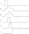
图13是当本发明所述的移位寄存器单元的第二具体实施例包括的各晶体管的阈值电压负漂至-3V时,各节点的电位的波形图;13 is a waveform diagram of the potential of each node when the threshold voltage of each transistor included in the second specific embodiment of the shift register unit according to the present invention drifts negatively to -3V;
图14是本发明实施例所述的栅极驱动电路包括的四级移位寄存器单元的连接关系示意图;14 is a schematic diagram of the connection relationship of the four-stage shift register unit included in the gate drive circuit according to the embodiment of the present invention;
图15是本发明实施例所述的栅极驱动电路采用的各时钟信号的波形图。FIG. 15 is a waveform diagram of each clock signal used by the gate driving circuit according to the embodiment of the present invention.
具体实施方式Detailed ways
下面将结合本发明实施例中的附图,对本发明实施例中的技术方案进行清楚、完整地描述,显然,所描述的实施例仅仅是本发明一部分实施例,而不是全部的实施例。基于本发明中的实施例,本领域普通技术人员在没有做出创造性劳动前提下所获得的所有其他实施例,都属于本发明保护的范围。The technical solutions in the embodiments of the present invention will be clearly and completely described below with reference to the accompanying drawings in the embodiments of the present invention. Obviously, the described embodiments are only a part of the embodiments of the present invention, but not all of the embodiments. Based on the embodiments of the present invention, all other embodiments obtained by those of ordinary skill in the art without creative efforts shall fall within the protection scope of the present invention.
本发明所有实施例中采用的晶体管均可以为三极管、薄膜晶体管或场效应管或其他特性相同的器件。在本发明实施例中,为区分晶体管除控制极之外的两极,将其中一极称为第一极,另一极称为第二极。The transistors used in all embodiments of the present invention may be triodes, thin film transistors, field effect transistors, or other devices with the same characteristics. In the embodiment of the present invention, in order to distinguish the two poles of the transistor except the control pole, one pole is called the first pole, and the other pole is called the second pole.
在实际操作时,当所述晶体管为三极管时,所述控制极可以为基极,所述第一极可以为集电极,所述第二极可以发射极;或者,所述控制极可以为基极,所述第一极可以为发射极,所述第二极可以集电极。In actual operation, when the transistor is a triode, the control electrode may be the base electrode, the first electrode may be the collector electrode, and the second electrode may be the emitter electrode; or the control electrode may be the base electrode electrode, the first electrode can be an emitter electrode, and the second electrode can be a collector electrode.
在实际操作时,当所述晶体管为薄膜晶体管或场效应管时,所述控制极可以为栅极,所述第一极可以为漏极,所述第二极可以为源极;或者,所述控制极可以为栅极,所述第一极可以为源极,所述第二极可以为漏极。In actual operation, when the transistor is a thin film transistor or a field effect transistor, the control electrode may be a gate electrode, the first electrode may be a drain electrode, and the second electrode may be a source electrode; The control electrode may be a gate electrode, the first electrode may be a source electrode, and the second electrode may be a drain electrode.
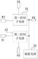
如图1所示,本发明实施例所述的移位寄存器单元包括下拉节点控制电路10;As shown in FIG. 1 , the shift register unit according to the embodiment of the present invention includes a pull-down
所述下拉节点控制电路10分别与输入端I1、复位端R1、第一电压端V1、第二电压端V2和下拉节点P2电连接,用于在所述输入端I1提供的输入信号和所述复位端R1提供的复位信号的控制下,控制所述下拉节点P2与所述第一电压端V1或所述第二电压端V2连通,并控制维持所述下拉节点P2的电位。The pull-down
在相关的移位寄存器单元中,需要通过反相器来控制下拉节点的电位,这种方法需要利用大量TFT(薄膜晶体管)形成反相器,同时反相器受到TFT的阈值电压漂移的影响,会导致电路信赖性较低。In the relevant shift register unit, the potential of the pull-down node needs to be controlled by an inverter. This method needs to use a large number of TFTs (thin film transistors) to form an inverter, and the inverter is affected by the threshold voltage shift of the TFT. It will lead to lower circuit reliability.
本发明实施例所述的移位寄存器单元采用下拉节点控制电路10以控制下拉节点P2的电位,解决相关的移位寄存器单元需要采用反相器控制下拉节点的电位,从而导致的电路信赖性低的问题,以使得本发明实施例所述的移位寄存器单元的结构简单,减少采用的晶体管的数目,利于实现高PPI(Pixels Per Inch,每英寸所拥有的像素数量),信赖性高。The shift register unit according to the embodiment of the present invention adopts the pull-down
本发明实施例所述的移位寄存器单元在工作时,在输入端I1提供的输入信号的控制下,下拉节点控制电路10控制下拉节点P2与第一电压端V1之间连通,在复位端R1提供的复位信号的控制下,下拉节点控制电路10控制下拉节点P2与第二电压端电连接,所述下拉节点控制电路10控制维持下拉节点P2的电位。When the shift register unit according to the embodiment of the present invention is working, under the control of the input signal provided by the input terminal I1, the pull-down
在本发明实施例中,所述第一电压端V1提供的第一电压可以为高电压Vdd,所述第二电压端V2提供的第二电压可以为第一低电压LVGL1,但不以此为限。当下拉节点P2控制的用于控制栅极驱动信号的晶体管为p型晶体管时,第一电压可以为低电压,第二电压可以为高电压。In the embodiment of the present invention, the first voltage provided by the first voltage terminal V1 may be the high voltage Vdd, and the second voltage provided by the second voltage terminal V2 may be the first low voltage LVGL1, but not limit. When the transistor for controlling the gate driving signal controlled by the pull-down node P2 is a p-type transistor, the first voltage may be a low voltage, and the second voltage may be a high voltage.
在本发明实施例中,所述输入端I1可以与相邻上一级移位寄存器单元的进位信号输出端电连接,第g级移位寄存器单元的复位端可以与第g+2级移位寄存器单元的进位信号输出端电连接,g为正整数,但不以此为限。In this embodiment of the present invention, the input terminal I1 may be electrically connected to the carry signal output terminal of the adjacent previous-stage shift register unit, and the reset terminal of the g-th stage shift register unit may be connected to the g+2-th stage shift register unit. The carry signal output end of the register unit is electrically connected, and g is a positive integer, but not limited thereto.
本发明实施例所述的移位寄存器单元在工作时,显示周期可以包括依次设置的输入时间段、输出时间段和复位时间段;When the shift register unit described in the embodiment of the present invention is working, the display period may include an input time period, an output time period and a reset time period that are set in sequence;
在输入时间段,在输入端I1提供的输入信号的控制下,下拉节点控制电路10控制下拉节点P2与第一电压端V1之间连通,以控制下拉节点P2的电位为高电压;During the input period, under the control of the input signal provided by the input terminal I1, the pull-down
在输出时间段,下拉节点控制电路10控制维持下拉节点P2的电位为高电压;During the output period, the pull-down
在复位时间段,在复位端R1提供的复位信号的控制下,下拉节点控制电路10控制下拉节点P2与第二电压端V2之间连通,以控制下拉节点P2的电位为低电压。During the reset period, under the control of the reset signal provided by the reset terminal R1, the pull-down
如图2所示,在图1所示的实施例的基础上,所述下拉节点控制电路10可以包括第一控制子电路11、第二控制子电路12和储能电路13;As shown in FIG. 2 , on the basis of the embodiment shown in FIG. 1 , the pull-down
所述第一控制子电路11分别与所述复位端R1、所述下拉节点P2和所述第一电压端V1电连接,用于在所述复位信号的控制下,控制所述下拉节点P2与所述第一电压端V1之间连通;The
所述第二控制子电路12分别与所述输入端I1、所述下拉节点P2和所述第二电压端V2电连接,用于在所述输入信号的控制下,控制所述下拉节点P2与所述第二电压端V2之间连通;The
所述储能电路13与所述下拉节点P2电连接,用于维持所述下拉节点P2的电位。The
本发明如图2所示的移位寄存器单元的实施例在工作时,When the embodiment of the shift register unit shown in FIG. 2 of the present invention is working,
在输入时间段,在输入端I1提供的输入信号的控制下,第二控制子电路12控制下拉节点P2与第一电压端V1之间连通;During the input period, under the control of the input signal provided by the input terminal I1, the second control sub-circuit 12 controls the connection between the pull-down node P2 and the first voltage terminal V1;
在输出时间段,储能电路13维持下拉节点P2的电位;During the output period, the
在复位时间段,在复位端R1提供的复位信号的控制下,第一控制子电路11控制下拉节点P2与第二电压端V2之间连通。During the reset period, under the control of the reset signal provided by the reset terminal R1, the
在具体实施时,所述第一控制子电路可以包括第一控制晶体管,所述第二控制子电路包括第二控制晶体管,所述储能电路包括存储电容;In a specific implementation, the first control sub-circuit may include a first control transistor, the second control sub-circuit may include a second control transistor, and the energy storage circuit may include a storage capacitor;
所述第一控制晶体管的控制极与所述复位端电连接,所述第一控制晶体管的第一极与所述第一电压端电连接,所述第一控制晶体管的第二极与所述下拉节点电连接;The control electrode of the first control transistor is electrically connected to the reset terminal, the first electrode of the first control transistor is electrically connected to the first voltage terminal, and the second electrode of the first control transistor is electrically connected to the first voltage terminal. The pull-down node is electrically connected;
所述第二控制晶体管的控制极与所述输入端电连接,所述第二控制晶体管的第一极与所述下拉节点电连接,所述第二控制晶体管的第二极与所述第二电压端电连接;The control electrode of the second control transistor is electrically connected to the input terminal, the first electrode of the second control transistor is electrically connected to the pull-down node, and the second electrode of the second control transistor is electrically connected to the second control transistor. The voltage terminal is electrically connected;
所述存储电容的第一端与所述下拉节点电连接,所述存储电容的第二端与所述第二电压端电连接。The first terminal of the storage capacitor is electrically connected to the pull-down node, and the second terminal of the storage capacitor is electrically connected to the second voltage terminal.
如图3所示,在图2所示的移位寄存器单元的实施例的基础上,所述第一控制子电路11可以包括第一控制晶体管T3,所述第二控制子电路12包括第二控制晶体管T4,所述储能电路13包括存储电容C1;As shown in FIG. 3, on the basis of the embodiment of the shift register unit shown in FIG. 2, the
所述第一控制晶体管T3的栅极与所述复位端R1电连接,所述第一控制晶体管T3的漏极与所述第一电压端V1电连接,所述第一控制晶体管T3的源极与所述下拉节点P2电连接;The gate of the first control transistor T3 is electrically connected to the reset terminal R1, the drain of the first control transistor T3 is electrically connected to the first voltage terminal V1, and the source of the first control transistor T3 electrically connected to the pull-down node P2;
所述第二控制晶体管T4的栅极与所述输入端I1电连接,所述第二控制晶体管T4的漏极与所述下拉节点P2电连接,所述第二控制晶体管T4的源极与所述第二电压端V2电连接;The gate of the second control transistor T4 is electrically connected to the input terminal I1, the drain of the second control transistor T4 is electrically connected to the pull-down node P2, and the source of the second control transistor T4 is electrically connected to the pull-down node P2. the second voltage terminal V2 is electrically connected;
所述存储电容C1的第一端与所述下拉节点P2电连接,所述存储电容的第二端与所述第二电压端V2电连接。The first terminal of the storage capacitor C1 is electrically connected to the pull-down node P2, and the second terminal of the storage capacitor is electrically connected to the second voltage terminal V2.
在图3所示的实施例中,T3和T4可以为n型薄膜晶体管,但不以此为限。In the embodiment shown in FIG. 3 , T3 and T4 may be n-type thin film transistors, but not limited thereto.
本发明如图3所示的移位寄存器单元的实施例在工作时,When the embodiment of the shift register unit shown in FIG. 3 of the present invention is working,
在输入时间段,I1提供高电压,R1提供低电压,T4打开,T3关断,P2与第二电压端V2之间连通;During the input period, I1 provides a high voltage, R1 provides a low voltage, T4 is turned on, T3 is turned off, and the connection between P2 and the second voltage terminal V2;
在输出时间段,I1和R1都提供低电压,T3和T4关断,C1维持P2的电位;During the output period, both I1 and R1 provide low voltage, T3 and T4 are turned off, and C1 maintains the potential of P2;
在复位时间段,I1提供低电压,R1提供高电压,T4关断,T3打开,P2与第一电压端V1之间连通。In the reset period, I1 provides a low voltage, R1 provides a high voltage, T4 is turned off, T3 is turned on, and the connection between P2 and the first voltage terminal V1 is connected.
可选的,所述第一控制子电路包括第一控制晶体管,所述第二控制子电路可以包括第二控制晶体管和第三控制晶体管;Optionally, the first control sub-circuit includes a first control transistor, and the second control sub-circuit may include a second control transistor and a third control transistor;
所述第一控制晶体管的控制极与所述复位端电连接,所述第一控制晶体管的第一极与所述第一电压端电连接,所述第一控制晶体管的第二极与所述下拉节点电连接;The control electrode of the first control transistor is electrically connected to the reset terminal, the first electrode of the first control transistor is electrically connected to the first voltage terminal, and the second electrode of the first control transistor is electrically connected to the first voltage terminal. The pull-down node is electrically connected;
所述第二控制晶体管的控制极与所述输入端电连接,所述第二控制晶体管的第一极与所述下拉节点电连接;The control electrode of the second control transistor is electrically connected to the input terminal, and the first electrode of the second control transistor is electrically connected to the pull-down node;
所述存储电容的第一端与所述下拉节点电连接,所述存储电容的第二端与所述第二电压端电连接;The first end of the storage capacitor is electrically connected to the pull-down node, and the second end of the storage capacitor is electrically connected to the second voltage end;
所述第三控制晶体管的控制极与所述输入端电连接,所述第三控制晶体管的第一极与所述第二控制晶体管的第二极电连接,所述第三控制晶体管的第二极与所述第二电压端电连接。The control electrode of the third control transistor is electrically connected to the input terminal, the first electrode of the third control transistor is electrically connected to the second electrode of the second control transistor, and the second electrode of the third control transistor is electrically connected. The pole is electrically connected to the second voltage terminal.
在优选情况下,所述第二控制子电路还可以包括第三控制晶体管,第三控制晶体管和第二控制晶体管相互串联,以提升与C1并联的下拉节点P2与第二电压端V2之间的通断电路上的电阻,防止输入信号长时间作用于T4而导致T4负漂而使得T4产生漏电而产生的无法维持上拉节点的电位的问题。In a preferred case, the second control sub-circuit may further include a third control transistor, and the third control transistor and the second control transistor are connected in series with each other to increase the voltage between the pull-down node P2 connected in parallel with C1 and the second voltage terminal V2 The resistance on the switch-on circuit prevents the problem that the potential of the pull-up node cannot be maintained due to the input signal acting on T4 for a long time, resulting in negative drift of T4 and leakage of T4.
在优选情况下,所述复位端提供的复位信号也可以为下拉控制时钟信号,以使得在复位时间段和输出截止保持时间段,第一控制晶体管T3每隔预定时间就打开,以不断为C1充电,能够保证维持P2的电位,降低噪声。In a preferred case, the reset signal provided by the reset terminal can also be a pull-down control clock signal, so that during the reset period and the output cut-off holding period, the first control transistor T3 is turned on every predetermined time, so as to continuously supply C1 Charging can ensure that the potential of P2 is maintained and noise is reduced.
在本发明实施例中,所述显示周期可以包括依次设置的输入时间段、输出时间段、复位时间段和输出截止保持时间段;In this embodiment of the present invention, the display period may include an input time period, an output time period, a reset time period, and an output cutoff hold time period that are set in sequence;
在所述输入时间段和所述输出时间段,所述下拉控制时钟信号的电位为无效电压,以使得所述第一控制子电路11在所述复位信号的控制下,控制所述下拉节点P2与所述第一电压端V1之间断开;During the input period and the output period, the potential of the pull-down control clock signal is an inactive voltage, so that the
在所述复位时间段,所述下拉控制时钟信号的电位为第一有效电压,以使得所述第一控制子电路11在所述复位信号的控制下,控制所述下拉节点P2与所述第一电压端V1之间连通;During the reset period, the potential of the pull-down control clock signal is a first effective voltage, so that the
所述输出截止保持时间段包括依次设置的多个输出截止保持阶段;The output cut-off hold time period includes a plurality of output cut-off hold stages set in sequence;
所述输出截止保持阶段包括依次设置的第一子阶段和第二子阶段;The output cut-off holding stage includes a first sub-stage and a second sub-stage arranged in sequence;
在第一子阶段,所述下拉控制时钟信号的电位为无效电压,以使得所述第一控制子电路11在所述复位信号的控制下,控制所述下拉节点P2与所述第一电压端V1之间断开;In the first sub-phase, the potential of the pull-down control clock signal is an inactive voltage, so that the
在第二子阶段,所述下拉控制时钟信号的电位为第一有效电压,以使得所述第一控制子电路11在所述复位信号的控制下,控制所述下拉节点P2与所述第一电压端V1之间连通。In the second sub-phase, the potential of the pull-down control clock signal is a first effective voltage, so that the
在本实施例中,当所述第一控制子电路11包括的晶体管为n型晶体管时,所述无效电压为低电压,所述第一有效电压为高电压;当所述第一控制子电路11包括的晶体管为p型晶体管时,所述无效电压为高电压,所述第一有效电压为低电压;但不以此为限。In this embodiment, when the transistors included in the
在具体实施时,所述移位寄存器单元还可以包括置位电路、上拉节点电位维持电路和N个上拉节点;In a specific implementation, the shift register unit may further include a setting circuit, a pull-up node potential maintaining circuit, and N pull-up nodes;
所述置位电路包括相互串联的N个置位子电路,N为大于或等于2的整数;所述上拉节点电位维持电路包括N个电位维持子电路;The setting circuit includes N setting sub-circuits connected in series, where N is an integer greater than or equal to 2; the pull-up node potential maintaining circuit includes N potential maintaining sub-circuits;
第一置位子电路的控制端与所述输入端电连接,所述第一置位子电路的第一端与第一电压端电连接,所述第一置位子电路的第二端与第一上拉节点电连接,所述第一置位子电路用于在所述输入信号的控制下,控制第一上拉节点与所述第一电压端之间连通;The control terminal of the first setting sub-circuit is electrically connected to the input terminal, the first terminal of the first setting sub-circuit is electrically connected to the first voltage terminal, and the second terminal of the first setting sub-circuit is electrically connected to the first upper The pull-up node is electrically connected, and the first set sub-circuit is configured to control the connection between the first pull-up node and the first voltage terminal under the control of the input signal;
第n置位子电路的控制端与所述输入端电连接,所述第n置位子电路的第一端与第n-1上拉节点电连接,所述第n置位子电路的第二端与第n上拉节点电连接;所述第n置位子电路用于在所述输入信号的控制下,控制所述第n-1上拉节点与所述第n上拉节点之间连通;n为大于1而小于或等于N的整数;The control terminal of the nth set sub-circuit is electrically connected to the input terminal, the first terminal of the nth set sub-circuit is electrically connected to the n-1th pull-up node, and the second terminal of the nth set sub-circuit is electrically connected to the n-1th pull-up node. The nth pull-up node is electrically connected; the nth set sub-circuit is used to control the connection between the n-1th pull-up node and the nth pull-up node under the control of the input signal; n is an integer greater than 1 and less than or equal to N;
第一电位维持子电路与所述第一上拉节点电连接,用于维持所述第一上拉节点的电位;a first potential maintaining subcircuit is electrically connected to the first pull-up node for maintaining the potential of the first pull-up node;
第n电位维持子电路与所述第n上拉节点电连接,用于维持所述第n上拉节点的电位。The nth potential maintaining subcircuit is electrically connected to the nth pull-up node for maintaining the potential of the nth pull-up node.
在相关技术中,当相关的包括多级移位寄存器单元的栅极驱动电路同时驱动至少两行像素电路时,通过一个上拉节点来控制输出至少两级栅极驱动信号,相关的栅极驱动电路提供至所述至少两行像素电路的栅极驱动信号的下降时间tf差异较大。而在相关技术中,移位寄存器单元分离形成至少两个上拉节点需要额外的信号长时间作用于晶体管的栅极,或者需要TFT组成二极管结构,前者不利于信赖性,后者会损失分离后的上拉节点的电压,本发明实施例通过置位电路包括多级相互串联的置位子电路可以避免以上问题。In the related art, when a related gate driving circuit including a multi-stage shift register unit drives at least two rows of pixel circuits simultaneously, a pull-up node is used to control the output of at least two stages of gate driving signals, and the related gate driving The falling times tf of the gate driving signals provided by the circuit to the at least two rows of pixel circuits are quite different. In the related art, the separation of the shift register unit to form at least two pull-up nodes requires an extra signal to act on the gate of the transistor for a long time, or requires the TFT to form a diode structure. The voltage of the pull-up node is higher than that of the embodiment of the present invention, the above problems can be avoided by the setting circuit including the setting sub-circuits in multiple stages connected in series with each other.
本发明实施例采用多级相互串联的置位子电路组成的置位电路,所述多级相互串联的置位子电路分别提供各个上拉节点的电位,每个上拉节点分别控制输出相应级栅极驱动信号,以减小所述移位寄存器单元输出的各级栅极驱动信号的下降时间tf的差异。The embodiment of the present invention adopts a set circuit composed of multiple sets of set sub-circuits connected in series. The multiple sets of set sub-circuits in series provide the potential of each pull-up node, and each pull-up node controls the output of the gate of the corresponding stage respectively. driving signals, so as to reduce the difference of the falling time tf of the gate driving signals of all levels output by the shift register unit.
下面以N等于2为例来说明本发明实施例所述的移位寄存器单元,但是在实际操作是,N也可以大于2。The shift register unit according to the embodiment of the present invention is described below by taking N equal to 2 as an example, but in actual operation, N may also be greater than 2.
如图4所示,在图1所示的移位寄存器单元的基础上,所述移位寄存器单元还可以包括置位电路40、上拉节点电位维持电路41、第一上拉节点P11和第二上拉节点P12;As shown in FIG. 4 , on the basis of the shift register unit shown in FIG. 1 , the shift register unit may further include a
所述置位电路40包括相互串联的第一置位子电路401和第二置位子电路402;The setting
所述上拉节点电位维持电路41包括第一电位维持子电路411和第二电位维持子电路412;The pull-up node
第一置位子电路401的控制端与所述输入端I1电连接,所述第一置位子电路401的第一端与第一电压端V1电连接,所述第一置位子电路401的第二端与第一上拉节点P11电连接,所述第一置位子电路401用于在所述输入信号的控制下,控制第一上拉节点P11与所述第一电压端V1之间连通;The control terminal of the
第二置位子电路402的控制端与所述输入端I1电连接,所述第二置位子电路402的第一端与第一上拉节点P11电连接,所述第二置位子电路402的第二端与第二上拉节点P12电连接;所述第二置位子电路402用于在所述输入信号的控制下,控制所述第一上拉节点P11与所述第二上拉节点P12之间连通;The control terminal of the
第一电位维持子电路411与所述第一上拉节点P11电连接,用于维持所述第一上拉节点P11的电位;The first
第二电位维持子电路412与所述第二上拉节点P12电连接,用于维持所述第二上拉节点P12的电位。The second
在本发明如图4所示的移位寄存器单元的实施例中,置位电路40包括相互串联的第一置位子电路401和第二置位子电路402,所述置位电路40分离控制第一上拉节点P11的电位和第二上拉节点P12的电位,第一电位维持子电路411维持所述第一上拉节点P11的电位,第二电位维持子电路维持所述第二上拉节点P12的电位。本发明实施例提供一种具有多级输出功能的移位寄存器单元,可用于窄边框显示(由于一级移位寄存器单元可以输出多级栅极驱动信号,以控制扫描多行像素驱动电路,因此减少栅极驱动电路包括的移位寄存器单元的级数),尤其适用于大尺寸OLED(有机发光二极管)显示,并通过置位子电路串联结构,避免了一级移位寄存器单元输出的多级栅极驱动信号之间的相互干扰。In the embodiment of the shift register unit shown in FIG. 4 of the present invention, the setting
可选的,所述第一置位子电路可以包括第一置位晶体管;所述第n置位子电路可以包括第n置位晶体管;Optionally, the first setting subcircuit may include a first setting transistor; the nth setting subcircuit may include an nth setting transistor;
所述第一置位晶体管的控制极与所述输入端电连接,所述第一置位晶体管的第一极与所述第一电压端电连接,所述第一置位晶体管的第二极与所述第一上拉节点电连接;The control electrode of the first setting transistor is electrically connected to the input terminal, the first electrode of the first setting transistor is electrically connected to the first voltage terminal, and the second electrode of the first setting transistor is electrically connected electrically connected to the first pull-up node;
所述第n置位晶体管的控制极与所述输入端电连接,所述第n置位晶体管的第一极与第n-1上拉节点电连接,所述第n置位晶体管的第二极与第n上拉节点电连接。The control electrode of the nth setting transistor is electrically connected to the input terminal, the first electrode of the nth setting transistor is electrically connected to the n-1th pull-up node, and the second electrode of the nth setting transistor is electrically connected The pole is electrically connected to the nth pull-up node.
如图5所示,在图4所示的移位寄存器单元的实施例的基础上,所述第一置位子电路401可以包括第一置位晶体管T1,所述第二置位子电路401可以包括第二置位晶体管T2;As shown in FIG. 5 , based on the embodiment of the shift register unit shown in FIG. 4 , the
T1的栅极与所述输入端I1电连接,T1的漏极与第一电压端V1电连接,T1的源极与第一上拉节点P11电连接;The gate of T1 is electrically connected to the input terminal I1, the drain of T1 is electrically connected to the first voltage terminal V1, and the source of T1 is electrically connected to the first pull-up node P11;
T2的栅极与所述输入端I1电连接,T2的漏极与第一上拉节点P11电连接,T2的源极与第二上拉节点P12电连接。The gate of T2 is electrically connected to the input terminal I1, the drain of T2 is electrically connected to the first pull-up node P11, and the source of T2 is electrically connected to the second pull-up node P12.
在图5所示的实施例中,T1和T2都为n型薄膜晶体管,但不以此为限。In the embodiment shown in FIG. 5 , both T1 and T2 are n-type thin film transistors, but not limited thereto.
在具体实施时,所述移位寄存器单元还可以包括N个栅极驱动信号输出端;In a specific implementation, the shift register unit may further include N gate driving signal output terminals;
所述第一电位维持子电路包括第一储能电容,所述第n电位维持子电路包括第n储能电容;The first potential maintaining subcircuit includes a first energy storage capacitor, and the nth potential maintaining subcircuit includes an nth energy storage capacitor;
所述第一储能电容的第一端与所述第一上拉节点电连接,所述第一储能电容的第二端与第一栅极驱动信号输出端电连接;The first end of the first energy storage capacitor is electrically connected to the first pull-up node, and the second end of the first energy storage capacitor is electrically connected to the first gate driving signal output end;
所述第n储能电容的第一端与所述第n上拉节点电连接,所述第n储能电容的第二端与第n栅极驱动信号输出端电连接。The first end of the nth energy storage capacitor is electrically connected to the nth pull-up node, and the second end of the nth energy storage capacitor is electrically connected to the nth gate driving signal output end.
本发明实施例所述的移位寄存器单元在工作时,在输出时间段包括的至少部分时间,第一储能电容自举拉升第一上拉节点的电位,第二储能电容自举拉升第二上拉节点的电位。When the shift register unit according to the embodiment of the present invention is working, during at least part of the time included in the output time period, the first energy storage capacitor bootstrap pulls up the potential of the first pull-up node, and the second energy storage capacitor bootstraps pulls up the potential of the first pull-up node. Raise the potential of the second pull-up node.
在本发明实施例中,所述移位寄存器单元还可以包括下拉电路;In this embodiment of the present invention, the shift register unit may further include a pull-down circuit;
所述下拉电路分别与所述下拉节点、所述N个上拉节点和第二电压端电连接,用于在所述下拉节点的电位的控制下,控制所述N个上拉节点分别与所述第二电压端之间连通;The pull-down circuit is electrically connected to the pull-down node, the N pull-up nodes and the second voltage terminal respectively, and is used for controlling the N pull-up nodes to be respectively connected to the pull-down node under the control of the potential of the pull-down node. communication between the second voltage terminals;
所述下拉电路用于在下拉节点的电位的控制下,控制对所述N个上拉节点的电位进行复位。The pull-down circuit is configured to control the potentials of the N pull-up nodes to be reset under the control of the potentials of the pull-down nodes.
优选的,所述移位寄存器单元可以包括反馈电路和下拉电路;Preferably, the shift register unit may include a feedback circuit and a pull-down circuit;
所述下拉电路分别与所述下拉节点、所述N个上拉节点和反馈节点电连接,用于在所述下拉节点的电位的控制下,控制所述N个上拉节点分别与所述反馈节点连通;The pull-down circuit is electrically connected to the pull-down node, the N pull-up nodes and the feedback node respectively, and is used for controlling the N pull-up nodes to be respectively connected to the feedback node under the control of the potential of the pull-down node node connection;
所述反馈电路分别与第一上拉节点、所述反馈节点、第一电压端和第二电压端电连接,用于在所述第一上拉节点的电位的控制下,控制所述反馈节点与第一电压端之间连通,在所述下拉节点的电位的控制下,控制所述反馈节点与所述第二电压端之间连通。The feedback circuit is electrically connected to a first pull-up node, the feedback node, a first voltage terminal and a second voltage terminal respectively, and is used for controlling the feedback node under the control of the potential of the first pull-up node It is connected with the first voltage terminal, and under the control of the potential of the pull-down node, the feedback node is controlled to be connected with the second voltage terminal.
在优选情况下,所述移位寄存器单元还可以包括反馈电路和下拉电路,反馈电路在第一上拉节点的电位的控制下,控制反馈节点与第一电压端之间连通,在下拉节点的电位的控制下,控制反馈节点与第二电压端之间连通;当第一上拉节点的电位为第二有效电压时,反馈节点与第一电压端之间连通,即使与各上拉节点直接电连接的晶体管产生漏电,也不会对各上拉节点的电位产生影响。In a preferred case, the shift register unit may further include a feedback circuit and a pull-down circuit, the feedback circuit is controlled by the potential of the first pull-up node to control the communication between the feedback node and the first voltage terminal, and the feedback circuit is controlled by the potential of the first pull-up node to communicate with the first voltage terminal. Under the control of the potential, the control feedback node is connected with the second voltage terminal; when the potential of the first pull-up node is the second effective voltage, the feedback node is connected with the first voltage terminal, even if it is directly connected with each pull-up node. Leakage of electrically connected transistors does not affect the potential of each pull-up node.
在具体实施时,当反馈电路包括的栅极与第一上拉节点电连接的晶体管为n型晶体管时,第二有效电压为高电压,当反馈电路包括的栅极与第一上拉节点电连接的晶体管为p型晶体管时,第二有效电压为低电压。In a specific implementation, when the transistor included in the feedback circuit whose gate is electrically connected to the first pull-up node is an n-type transistor, the second effective voltage is a high voltage, and when the gate included in the feedback circuit is electrically connected to the first pull-up node When the connected transistor is a p-type transistor, the second effective voltage is a low voltage.
如图6所示,在图4所示的移位寄存器单元的实施例的基础上,本发明实施例所述的移位寄存器单元还包括反馈电路60和下拉电路61;As shown in FIG. 6, on the basis of the embodiment of the shift register unit shown in FIG. 4, the shift register unit according to the embodiment of the present invention further includes a
所述下拉电路61分别与所述下拉节点P2、所述第一上拉节点P11、第二上拉节点P12和反馈节点F1电连接,用于在所述下拉节点P2的电位的控制下,控制所述第一上拉节点P11与所述反馈节点F1之间连通,并控制所述第二上拉节点P12与所述反馈节点F1之间连通;The pull-
所述反馈电路60分别与第一上拉节点P11、所述反馈节点F1、第一电压端V1和第二电压端V2电连接,用于在所述第一上拉节点P11的电位的控制下,控制所述反馈节点F1与第一电压端V1之间连通,在所述下拉节点P2的电位的控制下,控制所述反馈节点F1与所述第二电压端V2之间连通。The
本发明如图6所示的移位寄存器单元的实施例增加了反馈电路60,能够使得即使与各上拉节点直接电连接的晶体管产生漏电,也不会对各上拉节点的电位产生影响。The embodiment of the shift register unit of the present invention as shown in FIG. 6 adds a
本发明如图6所示的移位寄存器单元的实施例在工作时,当第一上拉节点P11的电位为第三有效电压时,反馈电路60在第一上拉节点P11的电位的控制下,控制反馈节点F1与第一电压端V1之间连通,以使得即使下拉电路包括的晶体管漏电时,各上拉节点的电位也不会下降而使得相应的栅极与各上拉节点电连接的晶体管不能正确的打开。When the embodiment of the shift register unit shown in FIG. 6 is in operation, when the potential of the first pull-up node P11 is the third effective voltage, the
在本发明实施例中,当反馈电路60包括的栅极与第一上拉节点P11电连接的晶体管为n型晶体管时,所述第三有效电压为高电压,当反馈电路60包括的栅极与第一上拉节点P11电连接的晶体管为p型晶体管时,所述第三有效电压为低电压。In this embodiment of the present invention, when the transistor included in the
可选的,所述反馈电路可以包括第一反馈晶体管和第二反馈晶体管;Optionally, the feedback circuit may include a first feedback transistor and a second feedback transistor;
所述第一反馈晶体管的控制极与所述第一上拉节点电连接,所述第一反馈晶体管的第一极与所述第一电压端电连接,所述第一反馈晶体管的第二极与所述反馈节点电连接;The control electrode of the first feedback transistor is electrically connected to the first pull-up node, the first electrode of the first feedback transistor is electrically connected to the first voltage terminal, and the second electrode of the first feedback transistor is electrically connected electrically connected to the feedback node;
所述第二反馈晶体管的控制极与所述下拉节点电连接,所述第二反馈晶体管的第一极与所述反馈节点电连接,所述第二反馈晶体管的第二极与所述第二电压端电连接。The control electrode of the second feedback transistor is electrically connected to the pull-down node, the first electrode of the second feedback transistor is electrically connected to the feedback node, and the second electrode of the second feedback transistor is electrically connected to the second feedback transistor. The voltage terminals are electrically connected.
如图7所示,所述反馈电路60可以包括第一反馈晶体管T7和第二反馈晶体管T9;As shown in FIG. 7 , the
所述第一反馈晶体管T7的栅极与所述第一上拉节点P11电连接,所述第一反馈晶体管T7的漏极与所述第一电压端V1电连接,所述第一反馈晶体管T7的源极与所述反馈节点F1电连接;The gate of the first feedback transistor T7 is electrically connected to the first pull-up node P11, the drain of the first feedback transistor T7 is electrically connected to the first voltage terminal V1, and the first feedback transistor T7 The source of is electrically connected to the feedback node F1;
所述第二反馈晶体管T9的栅极与所述下拉节点P2电连接,所述第二反馈晶体管T9的漏极与所述反馈节点F1电连接,所述第二反馈晶体管T9的源极与所述第二电压端V2电连接。The gate of the second feedback transistor T9 is electrically connected to the pull-down node P2, the drain of the second feedback transistor T9 is electrically connected to the feedback node F1, and the source of the second feedback transistor T9 is electrically connected to the pull-down node P2. The second voltage terminal V2 is electrically connected.
在图7所示的实施例中,T7和T9都为n型薄膜晶体管,但不以此为限。In the embodiment shown in FIG. 7 , both T7 and T9 are n-type thin film transistors, but not limited thereto.
本发明如图7所示的移位寄存器单元的实施例在工作时,When the embodiment of the shift register unit shown in FIG. 7 of the present invention is working,
当P11的电位为高电压时,T7打开,以控制F1与V1之间连通;When the potential of P11 is a high voltage, T7 is turned on to control the connection between F1 and V1;
当P11的电位为低电压时,T7关断;When the potential of P11 is low voltage, T7 is turned off;
当P2的电位为高电压时,T9打开,以控制F1与V2之间连通;When the potential of P2 is a high voltage, T9 is turned on to control the connection between F1 and V2;
当P2的电位为低电压时,T9关断。When the potential of P2 is low voltage, T9 is turned off.
在具体实施时,所述移位寄存器单元还可以包括驱动输出电路和N个栅极驱动信号输出端;所述驱动输出电路可以包括N个驱动输出子电路;In a specific implementation, the shift register unit may further include a drive output circuit and N gate drive signal output terminals; the drive output circuit may include N drive output sub-circuits;
第一驱动输出子电路分别与第一栅极驱动信号输出端、所述第一上拉节点、所述下拉节点、第一输出时钟信号端和第三电压端电连接,用于在所述第一上拉节点的电位的控制下,控制所述第一栅极驱动信号输出端与所述第一输出时钟信号端之间连通,在所述下拉节点的电位的控制下,控制所述第一栅极驱动信号输出端与所述第三电压端之间连通;The first drive output sub-circuit is respectively electrically connected with the first gate drive signal output terminal, the first pull-up node, the pull-down node, the first output clock signal terminal and the third voltage terminal, and is used for the Under the control of the potential of a pull-up node, the connection between the first gate driving signal output terminal and the first output clock signal terminal is controlled, and under the control of the potential of the pull-down node, the first gate driving signal output terminal is controlled to communicate with the first output clock signal terminal. Connecting between the gate driving signal output terminal and the third voltage terminal;
第n驱动输出子电路分别与第n栅极驱动信号输出端、所述第n上拉节点、所述下拉节点、第n输出时钟信号端和第三电压端电连接,用于在所述第n上拉节点的电位的控制下,控制所述第n栅极驱动信号输出端与所述第n输出时钟信号端之间连通,在所述下拉节点的电位的控制下,控制所述第n栅极驱动信号输出端与所述第三电压端之间连通。The nth driving output sub-circuit is respectively electrically connected to the nth gate driving signal output terminal, the nth pull-up node, the pull-down node, the nth output clock signal terminal and the third voltage terminal, and is used for the output of the nth gate driving signal. Under the control of the potential of the n pull-up node, the nth gate drive signal output terminal is controlled to communicate with the nth output clock signal terminal, and under the control of the potential of the pull-down node, the nth gate drive signal output terminal is controlled to communicate with the nth output clock signal terminal. The gate driving signal output terminal is communicated with the third voltage terminal.
本发明实施例所述的移位寄存器单元还可以包括N个驱动输出子电路,第一驱动输出子电路在第一上拉节点的电位和下拉节点的电位的控制下,控制第一栅极驱动信号输出端输出第一栅极驱动信号,第n驱动输出子电路在第n上拉节点的电位和下拉节点的电位的控制下,控制第n栅极驱动信号输出端输出第n栅极驱动信号。The shift register unit described in the embodiment of the present invention may further include N drive output sub-circuits, and the first drive output sub-circuit controls the first gate drive under the control of the potential of the first pull-up node and the potential of the pull-down node The signal output terminal outputs the first gate driving signal, and the nth driving output sub-circuit controls the nth gate driving signal output terminal to output the nth gate driving signal under the control of the potential of the nth pull-up node and the potential of the pull-down node. .
在本发明实施例中,所述移位寄存器单元还可以包括进位信号输出端和进位信号输出电路;In the embodiment of the present invention, the shift register unit may further include a carry signal output terminal and a carry signal output circuit;
所述进位信号输出电路分别与第一上拉节点、所述下拉节点、进位输出时钟信号端、所述进位信号输出端和第二电压端电连接,用于在所述第一上拉节点的电位的控制下,控制所述进位信号输出端与所述进位输出时钟信号端之间连通,在所述下拉节点的电位的控制下,控制所述进位信号输出端与所述第二电压端之间连通。The carry signal output circuit is respectively electrically connected to the first pull-up node, the pull-down node, the carry-out clock signal terminal, the carry-signal output terminal and the second voltage terminal, and is used for the connection between the first pull-up node and the second voltage terminal. Under the control of the potential, the connection between the carry signal output terminal and the carry output clock signal terminal is controlled, and the connection between the carry signal output terminal and the second voltage terminal is controlled under the control of the potential of the pull-down node. connection between.
本发明实施例所述的移位寄存器单元还可以包括进位信号输出电路,进位信号输出电路在第一上拉节点的电位和下拉节点的电位的控制下,控制进位信号输出端输出进位信号,所述进位信号用于为相邻下一级移位寄存器单元提供输入信号。The shift register unit described in the embodiment of the present invention may further include a carry signal output circuit, and the carry signal output circuit controls the carry signal output terminal to output a carry signal under the control of the potential of the first pull-up node and the potential of the pull-down node, so The carry signal is used to provide an input signal for the adjacent next-stage shift register unit.
如图8所示,在图6所示的移位寄存器单元的实施例的基础上,本发明实施例所述的移位寄存器单元还包括驱动输出电路、第一栅极驱动信号输出端G1、第二栅极驱动信号输出端G2、进位输出电路92和进位信号输出端J1;As shown in FIG. 8, on the basis of the embodiment of the shift register unit shown in FIG. 6, the shift register unit according to the embodiment of the present invention further includes a drive output circuit, a first gate drive signal output end G1, The second gate drive signal output terminal G2, the
所述驱动输出电路可以包括第一驱动输出子电路911和第二驱动输出子电路912;The drive output circuit may include a first
第一驱动输出子电路911分别与第一栅极驱动信号输出端G1、所述第一上拉节点P11、所述下拉节点P2、第一输出时钟信号端D1和第三电压端V3电连接,用于在所述第一上拉节点P11的电位的控制下,控制所述第一栅极驱动信号输出端G1与所述第一输出时钟信号端D1之间连通,在所述下拉节点P2的电位的控制下,控制所述第一栅极驱动信号输出端G1与所述第三电压端V3之间连通;The first
第二驱动输出子电路912分别与第二栅极驱动信号输出端G2、所述第二上拉节点P12、所述下拉节点P2、第二输出时钟信号端D2和第三电压端V3电连接,用于在所述第二上拉节点P12的电位的控制下,控制所述第二栅极驱动信号输出端G2与所述第二输出时钟信号端D2之间连通,在所述下拉节点P2的电位的控制下,控制所述第二栅极驱动信号输出端G2与所述第三电压端V3之间连通;The second
所述进位信号输出电路92分别与第一上拉节点P11、所述下拉节点P2、进位输出时钟信号端D0、所述进位信号输出端J1和第二电压端V2电连接,用于在所述第一上拉节点P11的电位的控制下,控制所述进位信号输出端J1与所述进位输出时钟信号端D0之间连通,在所述下拉节点P2的电位的控制下,控制所述进位信号输出端J1与所述第二电压端V2之间连通。The carry
在本发明实施例中,所述第三电压端可以用于提供第二低电压VGL,但不以此为限。In this embodiment of the present invention, the third voltage terminal may be used to provide the second low voltage VGL, but is not limited thereto.
下面通过两个具体实施例所述的移位寄存器单元。The following describes the shift register unit through two specific embodiments.
如图9所示,本发明所述的移位寄存器单元的第一具体实施例包括下拉节点控制电路10、置位电路40、上拉节点电位维持电路41、下拉电路61、驱动输出电路、第一栅极驱动信号输出端G1、第二栅极驱动信号输出端G2、进位输出电路92和进位信号输出端J1;As shown in FIG. 9, the first specific embodiment of the shift register unit of the present invention includes a pull-down
所述下拉节点控制电路10包括第一控制子电路、第二控制子电路和储能电路;The pull-down
所述第一控制子电路包括第一控制晶体管T3,所述第二控制子电路包括第二控制晶体管T4,所述储能电路包括存储电容C1;The first control sub-circuit includes a first control transistor T3, the second control sub-circuit includes a second control transistor T4, and the energy storage circuit includes a storage capacitor C1;
所述第一控制晶体管T3的栅极与所述复位端R1电连接,所述第一控制晶体管T3的漏极接入高电压Vdd,所述第一控制晶体管T3的源极与所述下拉节点P2电连接;The gate of the first control transistor T3 is electrically connected to the reset terminal R1, the drain of the first control transistor T3 is connected to a high voltage Vdd, and the source of the first control transistor T3 is connected to the pull-down node P2 electrical connection;
所述第二控制晶体管T4的栅极与所述输入端I1电连接,所述第二控制晶体管T4的漏极与所述下拉节点P2电连接,所述第二控制晶体管T4的源极接入第一低电压LVGL;The gate of the second control transistor T4 is electrically connected to the input terminal I1, the drain of the second control transistor T4 is electrically connected to the pull-down node P2, and the source of the second control transistor T4 is connected to the first low voltage LVGL;
所述存储电容C1的第一端与所述下拉节点P2电连接,所述存储电容的第二端接入第一低电压LVGL;The first end of the storage capacitor C1 is electrically connected to the pull-down node P2, and the second end of the storage capacitor is connected to the first low voltage LVGL;
所述置位电路40包括相互串联的第一置位子电路和第二置位子电路;The setting
所述上拉节点电位维持电路41包括第一电位维持子电路和第二电位维持子电路;The pull-up node
所述第一置位子电路包括第一置位晶体管T1,所述第二置位子电路包括第二置位晶体管T2;The first setting sub-circuit includes a first setting transistor T1, and the second setting sub-circuit includes a second setting transistor T2;
T1的栅极与所述输入端I1电连接,T1的漏极与第一电压端V1电连接,T1的源极与第一上拉节点P11电连接;The gate of T1 is electrically connected to the input terminal I1, the drain of T1 is electrically connected to the first voltage terminal V1, and the source of T1 is electrically connected to the first pull-up node P11;
T2的栅极与所述输入端I1电连接,T2的漏极与第一上拉节点P11电连接,T2的源极与第二上拉节点P12电连接;The gate of T2 is electrically connected to the input terminal I1, the drain of T2 is electrically connected to the first pull-up node P11, and the source of T2 is electrically connected to the second pull-up node P12;
所述第一电位维持子电路包括第一储能电容C2,所述第二电位维持子电路包括第二储能电容C3;The first potential maintenance sub-circuit includes a first energy storage capacitor C2, and the second potential maintenance sub-circuit includes a second energy storage capacitor C3;
所述第一储能电容C2的第一端与第一上拉节点P11电连接,所述第一储能电容C2的第二端与第一栅极驱动信号输出端G1电连接;The first end of the first energy storage capacitor C2 is electrically connected to the first pull-up node P11, and the second end of the first energy storage capacitor C2 is electrically connected to the first gate driving signal output end G1;
所述第二储能电容C3的第一端与所述第二上拉节点P12电连接,所述第二储能电容C3的第二端与第二栅极驱动信号输出端G2电连接;The first end of the second energy storage capacitor C3 is electrically connected to the second pull-up node P12, and the second end of the second energy storage capacitor C3 is electrically connected to the second gate driving signal output end G2;
所述下拉电路61包括第一下拉晶体管T8和第二下拉晶体管T6;The pull-
T8的栅极与下拉节点P2电连接,T8的漏极与第一上拉节点P11电连接,T8的源极接入第一低电压LVGL;The gate of T8 is electrically connected to the pull-down node P2, the drain of T8 is electrically connected to the first pull-up node P11, and the source of T8 is connected to the first low voltage LVGL;
T6的栅极与所述下拉节点P2电连接,T6的漏极与第二上拉节点P12电连接,T6的源极接入第一低电压LVGL;The gate of T6 is electrically connected to the pull-down node P2, the drain of T6 is electrically connected to the second pull-up node P12, and the source of T6 is connected to the first low voltage LVGL;
所述驱动输出电路包括第一驱动输出子电路911和第二驱动输出子电路912;The drive output circuit includes a first
所述第一驱动输出子电路911包括第一驱动输出晶体管T91和第二驱动输出晶体管T92;The first
T91的栅极与第一上拉节点P11电连接,T91的漏极与第一输出时钟信号端D1电连接,T91的源极与第一栅极驱动信号输出端G1电连接;The gate of T91 is electrically connected to the first pull-up node P11, the drain of T91 is electrically connected to the first output clock signal terminal D1, and the source of T91 is electrically connected to the first gate drive signal output terminal G1;
T92的栅极与下拉节点P2电连接,T92的漏极与所述第一栅极驱动信号输出端G1电连接,T92的源极接入第二低电压VGL;The gate of T92 is electrically connected to the pull-down node P2, the drain of T92 is electrically connected to the first gate driving signal output terminal G1, and the source of T92 is connected to the second low voltage VGL;
所述第二驱动输出子电路912包括第三驱动输出晶体管T93和第四驱动输出晶体管T94;The second
T93的栅极与第二上拉节点P12电连接,T93的漏极与第二输出时钟信号端D2电连接,T93的源极与第二栅极驱动信号输出端G2电连接;The gate of T93 is electrically connected to the second pull-up node P12, the drain of T93 is electrically connected to the second output clock signal terminal D2, and the source of T93 is electrically connected to the second gate drive signal output terminal G2;
T94的栅极与下拉节点P2电连接,T94的漏极与所述第二栅极驱动信号输出端G2电连接,T94的源极接入第二低电压VGL;The gate of T94 is electrically connected to the pull-down node P2, the drain of T94 is electrically connected to the second gate driving signal output terminal G2, and the source of T94 is connected to the second low voltage VGL;
所述进位信号输出电路92包括第一进位信号输出晶体管T21和第二进位信号输出晶体管T22;The carry
T21的栅极与第一上拉节点P11电连接,T21的漏极与进位输出时钟信号端D0电连接,T21的源极与进位信号输出端J1电连接;The gate of T21 is electrically connected to the first pull-up node P11, the drain of T21 is electrically connected to the carry output clock signal terminal D0, and the source of T21 is electrically connected to the carry signal output terminal J1;
T22的栅极与下拉节点P2电连接,T22的漏极与进位信号输出端J1电连接,T22的源极接入第一低电压LVGL。The gate of T22 is electrically connected to the pull-down node P2, the drain of T22 is electrically connected to the carry signal output terminal J1, and the source of T22 is connected to the first low voltage LVGL.
在图9所示的移位寄存器单元的第一具体实施例中,所有的晶体管都为n型薄膜晶体管,但不以此为限。In the first specific embodiment of the shift register unit shown in FIG. 9 , all transistors are n-type thin film transistors, but not limited thereto.
在图9所示的移位寄存器单元的第一具体实施例中,输入端I1与相邻上一级移位寄存器单元的进位信号输出端电连接。In the first specific embodiment of the shift register unit shown in FIG. 9 , the input terminal I1 is electrically connected to the carry signal output terminal of the adjacent upper-stage shift register unit.
在图9所示的移位寄存器单元的第一具体实施例中,所述第一电压端为提供高电压Vdd的电压端,所述第二电压端为提供第一低电压LVGL的电压端,所述第三电压端为提供第二低电压VGL的电压端。In the first specific embodiment of the shift register unit shown in FIG. 9 , the first voltage terminal is a voltage terminal for providing a high voltage Vdd, the second voltage terminal is a voltage terminal for providing a first low voltage LVGL, The third voltage terminal is a voltage terminal for providing the second low voltage VGL.
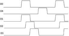
如图10所示,D1提供的第一输出时钟信号的周期T与D2提供的第二输出时钟信号的周期T相同,第二输出时钟信号比第一输出时钟信号延迟T/8,第一输出时钟信号的占空比与第二输出时钟信号的占空比相同,所述第一输出时钟信号的占空比可以为1/4,但不以此为限。As shown in Figure 10, the period T of the first output clock signal provided by D1 is the same as the period T of the second output clock signal provided by D2, the second output clock signal is delayed by T/8 from the first output clock signal, and the first output clock signal is The duty cycle of the clock signal is the same as that of the second output clock signal, and the duty cycle of the first output clock signal may be 1/4, but not limited thereto.
并在图10中,标号为D3的为第三输出时钟信号端提供的第三输出时钟信号,第三输出时钟信号比第二输出时钟信号延时T/2,第三输出时钟信号的周期与第一输出时钟信号的周期相同,第三输出时钟信号的占空比可以与第一输出时钟信号的周期相同。And in FIG. 10, the third output clock signal D3 is the third output clock signal provided by the third output clock signal terminal, the third output clock signal is delayed by T/2 than the second output clock signal, and the period of the third output clock signal is the same as that of the second output clock signal. The period of the first output clock signal is the same, and the duty cycle of the third output clock signal may be the same as the period of the first output clock signal.
如图10所示,D0提供的进位输出时钟信号可以与第一输出时钟信号相同,但不以此为限。As shown in FIG. 10 , the carry output clock signal provided by D0 may be the same as the first output clock signal, but not limited thereto.
如图11所示,本发明如图9所述的移位寄存器单元的第一具体实施例在工作时,显示周期包括依次设置的输入时间段t1、输出时间段t2、复位时间段t3和输出截止保持时间段t4;As shown in FIG. 11 , when the first specific embodiment of the shift register unit shown in FIG. 9 of the present invention is in operation, the display period includes an input period t1, an output period t2, a reset period t3 and an output period t1, which are set in sequence. end of hold time period t4;
在输入时间段t1,I1提供高电压,R1提供低电压,T1和T2打开,P11的电位和P12的电位被拉升;T3关断;T4打开,以控制P2接入LVGL;In the input period t1, I1 provides a high voltage, R1 provides a low voltage, T1 and T2 are turned on, the potential of P11 and the potential of P12 are pulled up; T3 is turned off; T4 is turned on to control P2 to access LVGL;
在输出时间段t2,I1和R1都提供低电压,T1、T2、T3和T4都关断;D1提供的第一输出时钟信号的电位和D2提供的第二输出时钟信号的电位依次上升为高电压,在第一输出时钟信号的电位上升为高电压,并经过预定时间T后,第一输出时钟信号的电位下降为低电压;在第二输出时钟信号的电位上升为高电压,并经过预定时间T后,第二输出时钟信号的电位下降为低电压;第一输出时钟信号的电位由低电压上升为高电压时,第一输出时钟信号通过C2自举拉升P11的电位,当第一输出时钟信号的电位由高电压下降为低电压时,C2相应控制下拉P11的电位;第二输出时钟信号的电位由低电压上升为高电压时,第二输出时钟信号通过C3自举拉升P12的电位,当第二输出时钟信号的电位由高电压下降为低电压时,C3相应控制下拉P12的电位;In the output period t2, both I1 and R1 provide low voltage, and T1, T2, T3 and T4 are all turned off; the potential of the first output clock signal provided by D1 and the potential of the second output clock signal provided by D2 rise to high in turn voltage, when the potential of the first output clock signal rises to a high voltage, and after a predetermined time T elapses, the potential of the first output clock signal drops to a low voltage; when the potential of the second output clock signal rises to a high voltage, and after a predetermined time T After time T, the potential of the second output clock signal drops to a low voltage; when the potential of the first output clock signal rises from a low voltage to a high voltage, the first output clock signal boosts the potential of P11 through the C2 bootstrap. When the potential of the output clock signal drops from a high voltage to a low voltage, C2 controls to pull down the potential of P11 accordingly; when the potential of the second output clock signal rises from a low voltage to a high voltage, the second output clock signal pulls up P12 through C3 bootstrapping When the potential of the second output clock signal drops from a high voltage to a low voltage, C3 correspondingly controls the potential of the pull-down P12;
在输入阶段t1和输出阶段t2,T91、T93和T21都打开,以使得G1与第一输出时钟信号端D1之间连通,使得G2与第二输出时钟信号端D2之间连通,并使得J1与进位输出时钟信号端D0之间连通;In the input phase t1 and the output phase t2, T91, T93 and T21 are all turned on, so that G1 is connected to the first output clock signal terminal D1, so that G2 is connected to the second output clock signal terminal D2, and J1 is connected to The carry output clock signal terminal D0 is connected;
在复位时间段t3,R1提供高电压,I1提供低电压,T1和T2关断,T3打开,P2接入高电压Vdd,T8和T6打开,以控制P11和P12都接入LVGL,控制T91、T93和T21都关断,并T92、T94和T22都打开,G1和G2都输出第二低电压VGL,J1输出第一低电压LVGL;In the reset period t3, R1 provides high voltage, I1 provides low voltage, T1 and T2 are turned off, T3 is turned on, P2 is connected to the high voltage Vdd, and T8 and T6 are turned on to control both P11 and P12 to be connected to LVGL, control T91, Both T93 and T21 are turned off, and T92, T94 and T22 are all turned on, G1 and G2 both output the second low voltage VGL, and J1 outputs the first low voltage LVGL;
在输出截止保持时间段t4,R1和I1都提供低电压,T1、T2、T3和T4都关断,C1维持P2的电位为高电压,T92、T94和T22都打开,G1和G2都输出第二低电压VGL,J1输出第一低电压LVGL。During the output cut-off hold time period t4, both R1 and I1 provide low voltage, T1, T2, T3 and T4 are all turned off, C1 maintains the potential of P2 at high voltage, T92, T94 and T22 are all turned on, G1 and G2 both output the first voltage The second low voltage VGL, J1 outputs the first low voltage LVGL.
由图11可知,G1输出的第一栅极驱动信号的下降时间和G2输出的第二栅极驱动信号的下降时间相差不大。It can be seen from FIG. 11 that the falling time of the first gate driving signal output by G1 and the falling time of the second gate driving signal output by G2 are not much different.
在图10和图11中,横轴是时间,纵轴是电位。In FIGS. 10 and 11 , the horizontal axis is time, and the vertical axis is potential.
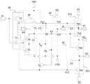
如图12所示,本发明所述的移位寄存器单元的第二具体实施例包括下拉节点控制电路10、置位电路40、上拉节点电位维持电路41、反馈电路、下拉电路、驱动输出电路、第一栅极驱动信号输出端G1、第二栅极驱动信号输出端G2、进位输出电路92和进位信号输出端J1;As shown in FIG. 12 , the second specific embodiment of the shift register unit of the present invention includes a pull-down
所述下拉节点控制电路10包括第一控制子电路、第二控制子电路和储能电路;The pull-down
所述第一控制子电路包括第一控制晶体管T3,所述第二控制子电路包括第二控制晶体管T4和第三控制晶体管T5,所述储能电路包括存储电容C1;The first control sub-circuit includes a first control transistor T3, the second control sub-circuit includes a second control transistor T4 and a third control transistor T5, and the energy storage circuit includes a storage capacitor C1;
所述第一控制晶体管T3的栅极与下拉控制时钟信号端D4电连接,所述第一控制晶体管T3的漏极接入高电压Vdd,所述第一控制晶体管T3的源极与所述下拉节点P2电连接;The gate of the first control transistor T3 is electrically connected to the pull-down control clock signal terminal D4, the drain of the first control transistor T3 is connected to a high voltage Vdd, and the source of the first control transistor T3 is connected to the pull-down control clock signal terminal D4. Node P2 is electrically connected;
所述第二控制晶体管T4的栅极与所述输入端I1电连接,所述第二控制晶体管T4的漏极与所述下拉节点P2电连接;The gate of the second control transistor T4 is electrically connected to the input terminal I1, and the drain of the second control transistor T4 is electrically connected to the pull-down node P2;
所述第三控制晶体管T5的栅极与所述输入端I1电连接,所述第三控制晶体管T5的漏极与所述第二控制晶体管T4的源极电连接,所述第三控制晶体管T5的源极接入第一低电压LVGL;The gate of the third control transistor T5 is electrically connected to the input terminal I1, the drain of the third control transistor T5 is electrically connected to the source of the second control transistor T4, and the third control transistor T5 The source is connected to the first low voltage LVGL;
所述存储电容C1的第一端与所述下拉节点P2电连接,所述存储电容的第二端接入第一低电压LVGL;The first end of the storage capacitor C1 is electrically connected to the pull-down node P2, and the second end of the storage capacitor is connected to the first low voltage LVGL;
所述置位电路40包括相互串联的第一置位子电路和第二置位子电路;The setting
所述上拉节点电位维持电路41包括第一电位维持子电路和第二电位维持子电路;The pull-up node
所述第一置位子电路包括第一置位晶体管T1,所述第二置位子电路包括第二置位晶体管T2;The first setting sub-circuit includes a first setting transistor T1, and the second setting sub-circuit includes a second setting transistor T2;
T1的栅极与所述输入端I1电连接,T1的漏极与第一电压端V1电连接,T1的源极与第一上拉节点P11电连接;The gate of T1 is electrically connected to the input terminal I1, the drain of T1 is electrically connected to the first voltage terminal V1, and the source of T1 is electrically connected to the first pull-up node P11;
T2的栅极与所述输入端I1电连接,T2的漏极与第一上拉节点P11电连接,T2的源极与第二上拉节点P12电连接;The gate of T2 is electrically connected to the input terminal I1, the drain of T2 is electrically connected to the first pull-up node P11, and the source of T2 is electrically connected to the second pull-up node P12;
所述第一电位维持子电路包括第一储能电容C2,所述第二电位维持子电路包括第二储能电容C3;The first potential maintenance sub-circuit includes a first energy storage capacitor C2, and the second potential maintenance sub-circuit includes a second energy storage capacitor C3;
所述第一储能电容C2的第一端与第一上拉节点P11电连接,所述第一储能电容C2的第二端与第一栅极驱动信号输出端G1电连接;The first end of the first energy storage capacitor C2 is electrically connected to the first pull-up node P11, and the second end of the first energy storage capacitor C2 is electrically connected to the first gate driving signal output end G1;
所述第二储能电容C3的第一端与所述第二上拉节点P12电连接,所述第二储能电容C3的第二端与第二栅极驱动信号输出端G2电连接;The first end of the second energy storage capacitor C3 is electrically connected to the second pull-up node P12, and the second end of the second energy storage capacitor C3 is electrically connected to the second gate driving signal output end G2;
所述下拉电路包括第一下拉晶体管T8和第二下拉晶体管T6;The pull-down circuit includes a first pull-down transistor T8 and a second pull-down transistor T6;
T8的栅极与下拉节点P2电连接,T8的漏极与第一上拉节点P11电连接,T8的源极与反馈节点F1电连接;The gate of T8 is electrically connected to the pull-down node P2, the drain of T8 is electrically connected to the first pull-up node P11, and the source of T8 is electrically connected to the feedback node F1;
T6的栅极与所述下拉节点P2电连接,T6的漏极与第二上拉节点P12电连接,T6的源极与反馈节点F1电连接;The gate of T6 is electrically connected to the pull-down node P2, the drain of T6 is electrically connected to the second pull-up node P12, and the source of T6 is electrically connected to the feedback node F1;
所述反馈电路包括第一反馈晶体管T7和第二反馈晶体管T9;The feedback circuit includes a first feedback transistor T7 and a second feedback transistor T9;
所述第一反馈晶体管T7的栅极与所述第一上拉节点P11电连接,所述第一反馈晶体管T7的漏极接入高电压Vdd,所述第一反馈晶体管T7的源极与所述反馈节点F1电连接;The gate of the first feedback transistor T7 is electrically connected to the first pull-up node P11, the drain of the first feedback transistor T7 is connected to the high voltage Vdd, and the source of the first feedback transistor T7 is connected to the high voltage Vdd. The feedback node F1 is electrically connected;
所述第二反馈晶体管T9的栅极与所述下拉节点P2电连接,所述第二反馈晶体管T9的漏极与所述反馈节点F1电连接,所述第二反馈晶体管T9的源极与接入第一低电压LVGL;The gate of the second feedback transistor T9 is electrically connected to the pull-down node P2, the drain of the second feedback transistor T9 is electrically connected to the feedback node F1, and the source of the second feedback transistor T9 is electrically connected to the pull-down node P2. into the first low voltage LVGL;
所述驱动输出电路包括第一驱动输出子电路911和第二驱动输出子电路912;The drive output circuit includes a first
所述第一驱动输出子电路911包括第一驱动输出晶体管T91和第二驱动输出晶体管T92;The first
T91的栅极与第一上拉节点P11电连接,T91的漏极与第一输出时钟信号端D1电连接,T91的源极与第一栅极驱动信号输出端G1电连接;The gate of T91 is electrically connected to the first pull-up node P11, the drain of T91 is electrically connected to the first output clock signal terminal D1, and the source of T91 is electrically connected to the first gate drive signal output terminal G1;
T92的栅极与下拉节点P2电连接,T92的漏极与所述第一栅极驱动信号输出端G1电连接,T92的源极接入第二低电压VGL;The gate of T92 is electrically connected to the pull-down node P2, the drain of T92 is electrically connected to the first gate driving signal output terminal G1, and the source of T92 is connected to the second low voltage VGL;
所述第二驱动输出子电路912包括第三驱动输出晶体管T93和第四驱动输出晶体管T94;The second
T93的栅极与第二上拉节点P12电连接,T93的漏极与第二输出时钟信号端D2电连接,T93的源极与第二栅极驱动信号输出端G2电连接;The gate of T93 is electrically connected to the second pull-up node P12, the drain of T93 is electrically connected to the second output clock signal terminal D2, and the source of T93 is electrically connected to the second gate drive signal output terminal G2;
T94的栅极与下拉节点P2电连接,T94的漏极与所述第二栅极驱动信号输出端G2电连接,T94的源极接入第二低电压VGL;The gate of T94 is electrically connected to the pull-down node P2, the drain of T94 is electrically connected to the second gate driving signal output terminal G2, and the source of T94 is connected to the second low voltage VGL;
所述进位信号输出电路92包括第一进位信号输出晶体管T21和第二进位信号输出晶体管T22;The carry
T21的栅极与第一上拉节点P11电连接,T21的漏极与进位输出时钟信号端D0电连接,T21的源极与进位信号输出端J1电连接;The gate of T21 is electrically connected to the first pull-up node P11, the drain of T21 is electrically connected to the carry output clock signal terminal D0, and the source of T21 is electrically connected to the carry signal output terminal J1;
T22的栅极与下拉节点P2电连接,T22的漏极与进位信号输出端J1电连接,T22的源极接入第一低电压LVGL。The gate of T22 is electrically connected to the pull-down node P2, the drain of T22 is electrically connected to the carry signal output terminal J1, and the source of T22 is connected to the first low voltage LVGL.
在图12所示的移位寄存器单元的第二具体实施例中,所有的晶体管都为n型薄膜晶体管,但不以此为限。In the second specific embodiment of the shift register unit shown in FIG. 12 , all transistors are n-type thin film transistors, but not limited thereto.
在图12所示的移位寄存器单元的第二具体实施例中,输入端I1与相邻上一级移位寄存器单元的进位信号输出端电连接。In the second specific embodiment of the shift register unit shown in FIG. 12 , the input terminal I1 is electrically connected to the carry signal output terminal of the adjacent upper-stage shift register unit.
在图12所示的移位寄存器单元的第二具体实施例中,所述第一电压端为提供高电压Vdd的电压端,所述第二电压端为提供第一低电压LVGL的电压端,所述第三电压端为提供第二低电压VGL的电压端。In the second specific embodiment of the shift register unit shown in FIG. 12 , the first voltage terminal is a voltage terminal for providing a high voltage Vdd, the second voltage terminal is a voltage terminal for providing a first low voltage LVGL, The third voltage terminal is a voltage terminal for providing the second low voltage VGL.
如图10所示,下拉控制时钟信号端D4提供的下拉控制时钟信号的周期T0与D0提供的进位输出时钟信号的周期T0相同,下拉控制时钟信号的占空比与进位输出时钟信号的占空比相同;As shown in Figure 10, the period T0 of the pull-down control clock signal provided by the pull-down control clock signal terminal D4 is the same as the period T0 of the carry-out clock signal provided by D0, and the duty cycle of the pull-down control clock signal is the same as the duty cycle of the carry-out clock signal. than the same;
下拉控制时钟信号比进位输出时钟信号延迟T0/2。The pull-down control clock signal is delayed T0/2 from the carry-out clock signal.
在本发明实施例中,所述下拉控制时钟信号的占空比可以为1/4,但不以此为限。In this embodiment of the present invention, the duty ratio of the pull-down control clock signal may be 1/4, but not limited thereto.
如图11所示,本发明如图12所述的移位寄存器单元的第二具体实施例在工作时,显示周期包括依次设置的输入时间段t1、输出时间段t2、复位时间段t3和输出截止保持时间段t4;As shown in FIG. 11 , when the second specific embodiment of the shift register unit shown in FIG. 12 of the present invention works, the display period includes an input period t1 , an output period t2 , a reset period t3 and an output period t1 , which are set in sequence. end of hold time period t4;
在输入时间段t1,I1提供高电压,R1提供低电压,T1和T2打开,P11的电位和P12的电位被拉升;T3关断;T4和T5打开,以控制P2接入LVGL;T7打开,以使得F1接入高电压Vdd,T8的源极和T6的源极都接入高电压Vdd,即使T8和T6漏电,也不会影响P11的电位和P12的电位;In the input period t1, I1 provides a high voltage, R1 provides a low voltage, T1 and T2 are turned on, the potential of P11 and the potential of P12 are pulled up; T3 is turned off; T4 and T5 are turned on to control P2 to access LVGL; T7 is turned on , so that F1 is connected to the high voltage Vdd, the source of T8 and the source of T6 are connected to the high voltage Vdd, even if T8 and T6 leak, it will not affect the potential of P11 and P12;
在输出时间段t2,I1和R1都提供低电压,T1、T2、T3和T4都关断;D1提供的第一输出时钟信号的电位和D2提供的第二输出时钟信号的电位依次上升为高电压,在第一输出时钟信号的电位上升为高电压,并经过预定时间T后,第一输出时钟信号的电位下降为低电压;在第二输出时钟信号的电位上升为高电压,并经过预定时间T后,第二输出时钟信号的电位下降为低电压;第一输出时钟信号的电位由低电压上升为高电压时,第一输出时钟信号通过C2自举拉升P11的电位,当第一输出时钟信号的电位由高电压下降为低电压时,C2相应控制下拉P11的电位;第二输出时钟信号的电位由低电压上升为高电压时,第二输出时钟信号通过C3自举拉升P12的电位,当第二输出时钟信号的电位由高电压下降为低电压时,C3相应控制下拉P12的电位;In the output period t2, both I1 and R1 provide low voltage, and T1, T2, T3 and T4 are all turned off; the potential of the first output clock signal provided by D1 and the potential of the second output clock signal provided by D2 rise to high in turn voltage, when the potential of the first output clock signal rises to a high voltage, and after a predetermined time T elapses, the potential of the first output clock signal drops to a low voltage; when the potential of the second output clock signal rises to a high voltage, and after a predetermined time T After time T, the potential of the second output clock signal drops to a low voltage; when the potential of the first output clock signal rises from a low voltage to a high voltage, the first output clock signal boosts the potential of P11 through the C2 bootstrap. When the potential of the output clock signal drops from a high voltage to a low voltage, C2 controls to pull down the potential of P11 accordingly; when the potential of the second output clock signal rises from a low voltage to a high voltage, the second output clock signal pulls up P12 through C3 bootstrapping When the potential of the second output clock signal drops from a high voltage to a low voltage, C3 correspondingly controls the potential of the pull-down P12;
在输出时间段t2,T7打开,以使得F1接入高电压Vdd,T8的源极和T6的源极都接入高电压Vdd,即使T8和T6漏电,也不会影响P11的电位和P12的电位;在输入阶段t1和输出阶段t2,T91、T93和T21都打开,以使得G1与第一输出时钟信号端D1之间连通,使得G2与第二输出时钟信号端D2之间连通,并使得J1与进位输出时钟信号端D0之间连通;In the output time period t2, T7 is turned on, so that F1 is connected to the high voltage Vdd, and the source of T8 and the source of T6 are connected to the high voltage Vdd. Even if T8 and T6 leak, it will not affect the potential of P11 and P12. potential; in the input stage t1 and the output stage t2, T91, T93 and T21 are all turned on, so that G1 is connected with the first output clock signal terminal D1, so that G2 is connected with the second output clock signal terminal D2, and make Connect between J1 and the carry output clock signal terminal D0;
在复位时间段t3,R1提供高电压,I1提供低电压,T1和T2关断,T3打开,P2接入高电压Vdd,T8和T6打开,以控制P11和P12都接入LVGL,控制T91、T93和T21都关断,并T92、T94和T22都打开,G1和G2都输出第二低电压VGL,J1输出第一低电压LVGL;T9打开,以使得F1接入第一低电压LVGL;In the reset period t3, R1 provides high voltage, I1 provides low voltage, T1 and T2 are turned off, T3 is turned on, P2 is connected to the high voltage Vdd, and T8 and T6 are turned on to control both P11 and P12 to be connected to LVGL, control T91, Both T93 and T21 are turned off, and T92, T94 and T22 are all turned on, G1 and G2 both output the second low voltage VGL, and J1 outputs the first low voltage LVGL; T9 is turned on, so that F1 is connected to the first low voltage LVGL;
在输出截止保持时间段t4,R1和I1都提供低电压,T1、T2、T3和T4都关断,C1维持P2的电位为高电压,T92、T94和T22都打开,G1和G2都输出第二低电压VGL,J1输出第一低电压LVGL;T9打开,以使得F1接入第一低电压LVGL;During the output cut-off hold time period t4, both R1 and I1 provide low voltage, T1, T2, T3 and T4 are all turned off, C1 maintains the potential of P2 at high voltage, T92, T94 and T22 are all turned on, G1 and G2 both output the first voltage Two low voltages VGL, J1 outputs the first low voltage LVGL; T9 is turned on, so that F1 is connected to the first low voltage LVGL;
在输出截止保持时间段,每隔一段时间,下拉控制时钟信号的电位变为高电压,当下拉控制时钟信号的电位为高电压时,T3打开,以为C1充电,以维持P2的电位为高电压。During the output cut-off hold time period, the potential of the pull-down control clock signal becomes a high voltage at regular intervals. When the potential of the pull-down control clock signal is a high voltage, T3 is turned on to charge C1 to maintain the potential of P2 at a high voltage. .
如图13所示,当如图12所示的移位寄存器单元的第二具体实施例包括的各晶体管的阈值电压负漂至-3V时,P11的电位、P12的电位和P2的电位可以很好的被维持,G1输出的第一栅极驱动信号的下降时间和G2的第二栅极驱动信号的下降时间一致。As shown in FIG. 13 , when the threshold voltages of the transistors included in the second specific embodiment of the shift register unit shown in FIG. 12 are negatively shifted to -3V, the potentials of P11 , P12 and P2 can be very high. Good is maintained, the falling time of the first gate driving signal output by G1 is consistent with the falling time of the second gate driving signal of G2.
在图13中,第一栅极驱动信号的下降时间是从a点到b点持续的时间,第二栅极驱动信号的下降时间是从c点到d点持续的时间。In FIG. 13 , the falling time of the first gate driving signal is the time lasting from point a to point b, and the falling time of the second gate driving signal is the time lasting from point c to point d.
在图13中,横轴是时间,纵轴是电位。In FIG. 13 , the horizontal axis is time, and the vertical axis is potential.
经过仿真,当图12所示的移位寄存器单元的阈值电压在-3.5V至+8V时,移位寄存器单元输出的两级栅极驱动信号的下降时间可以保持一致。After simulation, when the threshold voltage of the shift register unit shown in FIG. 12 is -3.5V to +8V, the falling time of the two-stage gate driving signal output by the shift register unit can be kept consistent.
本发明实施例所述的移位寄存器单元增加了反馈电路,可以应用于氧化物TFT背板和LTPS(低温多晶硅)背板。The shift register unit described in the embodiment of the present invention adds a feedback circuit, and can be applied to an oxide TFT backplane and an LTPS (low temperature polysilicon) backplane.
在本发明实施例中,以栅极驱动电路中的移位寄存器单元采用n型晶体管为例举例说明,但是在实际操作时,该移位寄存器单元也可以采用p型晶体管。In the embodiment of the present invention, the shift register unit in the gate driving circuit uses an n-type transistor as an example for illustration, but in actual operation, the shift register unit may also use a p-type transistor.
在具体实施时,氧化物TFT背板中的栅极驱动电路采用的晶体管为n型晶体管,所述n型晶体管的阈值电压会正向漂移或负向漂移,当n型晶体管的阈值电压负向漂移时会产生漏电,本发明实施例可以防止由于n型晶体管漏电而导致的不能很好的维持上拉节点的电位的现象;In specific implementation, the transistors used in the gate driving circuit in the oxide TFT backplane are n-type transistors, and the threshold voltage of the n-type transistors will shift positively or negatively. When the threshold voltage of the n-type transistors is negative Leakage will occur during drift, and the embodiment of the present invention can prevent the phenomenon that the potential of the pull-up node cannot be well maintained due to the leakage of n-type transistors;
LTPS背板中的栅极驱动电路采用的晶体管为p型晶体管,所述p型晶体管由于迁移率高而容易产生漏电,本发明实施例与可以防止由于p型晶体管漏电而导致的不能很好的维持上拉节点的电位的现象。The transistors used in the gate drive circuit in the LTPS backplane are p-type transistors, which are prone to leakage due to their high mobility. A phenomenon in which the potential of a pull-up node is maintained.
在本发明实施例中,以各晶体管为n型晶体管为例举例说明。In the embodiments of the present invention, each transistor is an n-type transistor as an example for illustration.
本发明实施例所述的移位寄存器单元的驱动方法,用于驱动本发明实施例所述的移位寄存器单元,所述移位寄存器单元的驱动方法包括:The driving method of the shift register unit according to the embodiment of the present invention is used for driving the shift register unit according to the embodiment of the present invention, and the driving method of the shift register unit includes:
下拉节点控制电路在输入端提供的输入信号的控制下,控制下拉节点与第二电压端之间连通,所述下拉节点控制电路在复位端提供的复位信号的控制下,控制下拉节点与第一电压端连通,所述下拉节点控制电路控制维持所述下拉节点的电位。The pull-down node control circuit controls the connection between the pull-down node and the second voltage end under the control of the input signal provided by the input end, and the pull-down node control circuit controls the pull-down node and the first voltage end under the control of the reset signal provided by the reset end. The voltage terminal is connected, and the pull-down node control circuit controls and maintains the potential of the pull-down node.
本发明实施例所述的移位寄存器单元的驱动方法采用下拉节点控制电路以控制下拉节点的电位,解决相关的移位寄存器单元需要采用反相器控制下拉节点的电位,从而导致的电路信赖性低的问题,以使得本发明实施例所述的移位寄存器单元的结构简单,减少采用的晶体管的数目,利于实现高PPI(Pixels Per Inch,每英寸所拥有的像素数量),信赖性高。The driving method of the shift register unit according to the embodiment of the present invention uses a pull-down node control circuit to control the potential of the pull-down node, and solves the problem that the related shift register unit needs to use an inverter to control the potential of the pull-down node, thereby causing circuit reliability. Therefore, the structure of the shift register unit described in the embodiment of the present invention is simple, the number of transistors used is reduced, and high PPI (Pixels Per Inch, the number of pixels per inch) is realized, and the reliability is high.
优选的,所述复位端提供的复位信号为下拉控制时钟信号,以使得在复位时间段和输出截止保持时间段,所述下拉节点控制电路能够更好的控制维持下拉节点的电位。Preferably, the reset signal provided by the reset terminal is a pull-down control clock signal, so that the pull-down node control circuit can better control and maintain the potential of the pull-down node during the reset period and the output off-hold period.
在优选情况下,所述移位寄存器单元还包括置位电路、上拉节点电位维持电路和N个上拉节点;所述置位电路包括相互串联的N个置位子电路,N为大于或等于2的整数;所述上拉节点电位维持电路包括N个电位维持子电路;所述移位寄存器单元的驱动方法还包括:In a preferred case, the shift register unit further includes a setting circuit, a pull-up node potential maintaining circuit and N pull-up nodes; the setting circuit includes N setting sub-circuits connected in series, and N is greater than or equal to an integer of 2; the pull-up node potential maintenance circuit includes N potential maintenance sub-circuits; the driving method of the shift register unit further includes:
第一置位子电路在所述输入信号的控制下,控制第一上拉节点与所述第一电压端之间连通;第一电位维持子电路维持所述第一上拉节点的电位;The first setting sub-circuit controls the connection between the first pull-up node and the first voltage terminal under the control of the input signal; the first potential maintaining sub-circuit maintains the potential of the first pull-up node;
第n置位子电路在所述输入信号的控制下,控制所述第n-1上拉节点与所述第n上拉节点之间连通;第n电位维持子电路维持所述第n上拉节点的电位。Under the control of the input signal, the nth setting subcircuit controls the connection between the n-1th pull-up node and the nth pull-up node; the nth potential maintaining subcircuit maintains the nth pull-up node the potential.
在本发明实施例中,所述移位寄存器单元可以包括置位电路,置位电路包括相互串联的N个置位子电路,多级相互串联的置位子电路分别提供各个上拉节点的电位,每个上拉节点分别控制输出相应级栅极驱动信号,以减小所述移位寄存器单元输出的各级栅极驱动信号的下降时间tf的差异。In this embodiment of the present invention, the shift register unit may include a setting circuit, and the setting circuit includes N setting sub-circuits connected in series with each other, and the multi-stage setting sub-circuits connected in series provide the potential of each pull-up node, respectively. Each pull-up node is controlled to output the gate driving signal of the corresponding stage, so as to reduce the difference of the falling time tf of the gate driving signal of each stage output by the shift register unit.
可选的,所述移位寄存器单元可以包括反馈电路和下拉电路;Optionally, the shift register unit may include a feedback circuit and a pull-down circuit;
所述移位寄存器单元的驱动方法还包括:The driving method of the shift register unit further includes:
所述下拉电路在所述下拉节点的电位的控制下,控制所述N个上拉节点分别与所述反馈节点连通;The pull-down circuit controls the N pull-up nodes to communicate with the feedback node respectively under the control of the potential of the pull-down node;
所述反馈电路在所述第一上拉节点的电位的控制下,控制所述反馈节点与第一电压端之间连通,在所述下拉节点的电位的控制下,控制所述反馈节点与所述第二电压端之间连通。Under the control of the potential of the first pull-up node, the feedback circuit controls the communication between the feedback node and the first voltage terminal, and under the control of the potential of the pull-down node, controls the feedback node to connect with the first voltage terminal. connected between the second voltage terminals.
在具体实施时,所述移位寄存器单元还包括驱动输出电路和N个栅极驱动信号输出端;所述驱动输出电路包括N个驱动输出子电路;所述移位寄存器单元的驱动方法还包括:In a specific implementation, the shift register unit further includes a drive output circuit and N gate drive signal output terminals; the drive output circuit includes N drive output sub-circuits; the driving method of the shift register unit further includes :
第一驱动输出子电路在所述第一上拉节点的电位的控制下,控制所述第一栅极驱动信号输出端与第一输出时钟信号端之间连通,在所述下拉节点的电位的控制下,控制所述第一栅极驱动信号输出端与第三电压端之间连通;Under the control of the potential of the first pull-up node, the first drive output sub-circuit controls the communication between the first gate drive signal output terminal and the first output clock signal terminal, and the potential of the pull-down node is lower than that of the pull-down node. under control, controlling the connection between the first gate drive signal output terminal and the third voltage terminal;
第n驱动输出子电路在所述第n上拉节点的电位的控制下,控制所述第n栅极驱动信号输出端与第n输出时钟信号端之间连通,在所述下拉节点的电位的控制下,控制所述第n栅极驱动信号输出端与所述第三电压端之间连通。Under the control of the potential of the nth pull-up node, the nth drive output sub-circuit controls the communication between the nth gate drive signal output terminal and the nth output clock signal terminal. Under the control, the nth gate driving signal output terminal is controlled to communicate with the third voltage terminal.
在本发明实施例中,所述移位寄存器单元还可以包括进位信号输出端和进位信号输出电路;所述移位寄存器单元的驱动方法还可以包括:In the embodiment of the present invention, the shift register unit may further include a carry signal output terminal and a carry signal output circuit; the driving method of the shift register unit may further include:
所述进位信号输出电路在所述第一上拉节点的电位的控制下,控制所述进位信号输出端与进位输出时钟信号端之间连通,在所述下拉节点的电位的控制下,控制所述进位信号输出端与第二电压端之间连通。Under the control of the potential of the first pull-up node, the carry signal output circuit controls the communication between the carry signal output terminal and the carry output clock signal terminal, and under the control of the potential of the pull-down node, controls the The carry signal output terminal is communicated with the second voltage terminal.
本发明实施例所述的栅极驱动电路包括多级上述的移位寄存器单元;The gate driving circuit according to the embodiment of the present invention includes multiple stages of the above-mentioned shift register unit;
所述移位寄存器单元包括进位信号输出端;The shift register unit includes a carry signal output terminal;
除了第一级移位寄存器单元之外,每一级移位寄存器单元的输入端都与相邻上一级移位寄存器单元的进位信号输出端电连接。Except for the first-stage shift register unit, the input end of each shift register unit is electrically connected to the carry signal output end of the adjacent previous-stage shift register unit.
图14中示出了本发明实施例所述的栅极驱动电路包括的四级移位寄存器单元;FIG. 14 shows the four-stage shift register unit included in the gate drive circuit according to the embodiment of the present invention;
如图14所示,标号为S4m-3的为栅极驱动电路包括的第4m-3级移位寄存器单元,标号为S4m-2的为栅极驱动电路包括的第4m-2级移位寄存器单元,标号为S4m-1的为栅极驱动电路包括的第4m-1级移位寄存器单元,标号为S4m的为栅极驱动电路包括的第4m级移位寄存器单元,其中,m为正整数;As shown in FIG. 14 , the 4m-3 stage shift register unit included in the gate drive circuit is labeled S4m-3, and the 4m-2 stage shift register included in the gate drive circuit is labeled S4m-2 The unit, labeled S4m-1 is the 4m-1st stage shift register unit included in the gate drive circuit, and the label S4m is the 4mth stage shift register unit included in the gate drive circuit, where m is a positive integer ;
S4m-3的进位输出时钟信号端D0接入第一时钟信号K1;S4m-3还可以接入第三时钟信号K3;The carry output clock signal terminal D0 of S4m-3 is connected to the first clock signal K1; S4m-3 can also be connected to the third clock signal K3;
S4m-2的进位输出时钟信号端D0接入第二时钟信号K2;S4m-2还可以接入第四时钟信号K4;The carry output clock signal terminal D0 of S4m-2 is connected to the second clock signal K2; S4m-2 can also be connected to the fourth clock signal K4;
S4m-1的进位输出时钟信号端D0接入第一时钟信号K1;S4m-1还可以接入第三时钟信号K3;The carry output clock signal terminal D0 of S4m-1 is connected to the first clock signal K1; S4m-1 can also be connected to the third clock signal K3;
S4m的进位输出时钟信号端D0接入第二时钟信号K2;S4m还可以接入第四时钟信号K4;The carry output clock signal terminal D0 of S4m is connected to the second clock signal K2; S4m can also be connected to the fourth clock signal K4;
S4m-3的进位信号输出端J1与S4m-2的输入端I1电连接;The carry signal output terminal J1 of S4m-3 is electrically connected to the input terminal I1 of S4m-2;
S4m-2的进位信号输出端J1与S4m-1的输入端I1电连接;The carry signal output terminal J1 of S4m-2 is electrically connected with the input terminal I1 of S4m-1;
S4m-1的进位信号输出端J1与S4m的输入端I1电连接;The carry signal output terminal J1 of S4m-1 is electrically connected to the input terminal I1 of S4m;
S4m-1的进位信号输出端J1与S4m-3的复位端R1电连接;The carry signal output terminal J1 of S4m-1 is electrically connected to the reset terminal R1 of S4m-3;
S4m的进位信号输出端J1与S4m-2的复位端R1电连接。The carry signal output terminal J1 of S4m is electrically connected to the reset terminal R1 of S4m-2.
并且,在图14所示的栅极驱动电路包括的四级移位寄存器单元中,S4m-1的第一输出时钟信号端接入第一输出时钟信号L1,S4m-1的第二输出时钟信号端接入第二输出时钟信号L2;S4m-2的第一输出时钟信号端接入第三输出时钟信号L3,S4m-1的第二输出时钟信号端接入第四输出时钟信号L4;S4m-3的第一输出时钟信号端接入第五输出时钟信号L5,S4m-1的第二输出时钟信号端接入第六输出时钟信号L6;S4m的第一输出时钟信号端接入第七输出时钟信号L7,S4m的第二输出时钟信号端接入第八输出时钟信号L8。In addition, in the four-stage shift register unit included in the gate drive circuit shown in FIG. 14, the first output clock signal terminal of S4m-1 is connected to the first output clock signal L1, and the second output clock signal of S4m-1 is connected The second output clock signal terminal of S4m-2 is connected to the second output clock signal L2; the first output clock signal terminal of S4m-2 is connected to the third output clock signal L3, and the second output clock signal terminal of S4m-1 is connected to the fourth output clock signal L4; The first output clock signal terminal of 3 is connected to the fifth output clock signal L5, the second output clock signal terminal of S4m-1 is connected to the sixth output clock signal L6; the first output clock signal terminal of S4m is connected to the seventh output clock signal The second output clock signal terminals of the signals L7 and S4m are connected to the eighth output clock signal L8.
如图15所示,K1的周期、K2的周期、K3的周期、K4的周期、L1的周期、L2的周期、L3的周期、L4的周期、L5的周期、L6的周期、L7的周期和L8的周期都为T;As shown in Figure 15, the period of K1, the period of K2, the period of K3, the period of K4, the period of L1, the period of L2, the period of L3, the period of L4, the period of L5, the period of L6, the period of L7 and the The period of L8 is T;
K1的占空比、K2的占空比、K3的占空比、K4的占空比、L1的占空比、L2的占空比、L3的占空比、L4的占空比、L5的占空比、L6的占空比、L7的占空比和L8的占空比都为1/4;K1 duty cycle, K2 duty cycle, K3 duty cycle, K4 duty cycle, L1 duty cycle, L2 duty cycle, L3 duty cycle, L4 duty cycle, L5 duty cycle The duty cycle, the duty cycle of L6, the duty cycle of L7 and the duty cycle of L8 are all 1/4;
K2比K1延迟T/4,K3比K2延迟T/4,K4比K3延迟T/4;K2 is delayed by T/4 compared with K1, K3 is delayed by T/4 compared with K2, and K4 is delayed by T/4 compared with K3;
L1比K4延迟T/4,L2比L1延迟T/8,L3比L2延迟T/8,L4比L3延迟T/8,L5比L4延迟T/8,L6比L5延迟T/8,L7比L6延迟T/8,L8比L7延迟T/8。L1 is T/4 later than K4, L2 is T/8 later than L1, L3 is T/8 later than L2, L4 is T/8 later than L3, L5 is T/8 later than L4, L6 is T/8 later than L5, and L7 is later than L7 L6 is delayed by T/8, and L8 is delayed by T/8 than L7.
本发明实施例所述的显示装置包括上述的栅极驱动电路。The display device according to the embodiment of the present invention includes the above-mentioned gate driving circuit.
本发明实施例所提供的显示装置可以为手机、平板电脑、电视机、显示器、笔记本电脑、数码相框、导航仪等任何具有显示功能的产品或部件。The display device provided by the embodiment of the present invention may be any product or component with a display function, such as a mobile phone, a tablet computer, a television, a monitor, a notebook computer, a digital photo frame, and a navigator.
以上所述是本发明的优选实施方式,应当指出,对于本技术领域的普通技术人员来说,在不脱离本发明所述原理的前提下,还可以作出若干改进和润饰,这些改进和润饰也应视为本发明的保护范围。The above are the preferred embodiments of the present invention. It should be pointed out that for those skilled in the art, without departing from the principles of the present invention, several improvements and modifications can be made. It should be regarded as the protection scope of the present invention.
Claims (18)
Priority Applications (3)
| Application Number | Priority Date | Filing Date | Title |
|---|---|---|---|
| CN202010191578.5ACN111179813B (en) | 2020-03-18 | 2020-03-18 | Shifting register unit, driving method, grid driving circuit and display device |
| PCT/CN2020/140585WO2021184899A1 (en) | 2020-03-18 | 2020-12-29 | Shift register unit, driving method, gate driving circuit, and display device |
| US17/417,518US11887683B2 (en) | 2020-03-18 | 2020-12-29 | Shift register unit, driving method, gate driving circuit and display device |
Applications Claiming Priority (1)
| Application Number | Priority Date | Filing Date | Title |
|---|---|---|---|
| CN202010191578.5ACN111179813B (en) | 2020-03-18 | 2020-03-18 | Shifting register unit, driving method, grid driving circuit and display device |
Publications (2)
| Publication Number | Publication Date |
|---|---|
| CN111179813A CN111179813A (en) | 2020-05-19 |
| CN111179813Btrue CN111179813B (en) | 2022-05-17 |
Family
ID=70655184
Family Applications (1)
| Application Number | Title | Priority Date | Filing Date |
|---|---|---|---|
| CN202010191578.5AActiveCN111179813B (en) | 2020-03-18 | 2020-03-18 | Shifting register unit, driving method, grid driving circuit and display device |
Country Status (3)
| Country | Link |
|---|---|
| US (1) | US11887683B2 (en) |
| CN (1) | CN111179813B (en) |
| WO (1) | WO2021184899A1 (en) |
Families Citing this family (5)
| Publication number | Priority date | Publication date | Assignee | Title |
|---|---|---|---|---|
| CN111179813B (en) | 2020-03-18 | 2022-05-17 | 合肥京东方卓印科技有限公司 | Shifting register unit, driving method, grid driving circuit and display device |
| US11574597B2 (en) | 2020-10-27 | 2023-02-07 | Boe Technology Group Co., Ltd. | Gate driving unit having node isolation |
| CN115398518B (en)* | 2021-01-28 | 2025-05-27 | 京东方科技集团股份有限公司 | Gate driving circuit and driving method thereof and display panel |
| CN119604919A (en)* | 2023-04-26 | 2025-03-11 | 京东方科技集团股份有限公司 | Driving circuit and display substrate |
| CN116825015B (en)* | 2023-06-21 | 2025-07-11 | 京东方科技集团股份有限公司 | Driving circuit, driving method and display device |
Citations (7)
| Publication number | Priority date | Publication date | Assignee | Title |
|---|---|---|---|---|
| KR20140079106A (en)* | 2012-12-18 | 2014-06-26 | 엘지디스플레이 주식회사 | Gate shift register and display device using the same |
| CN105761758A (en)* | 2016-05-18 | 2016-07-13 | 京东方科技集团股份有限公司 | Shifting register unit, driving method, grid driving circuit and display device |
| KR20180057975A (en)* | 2016-11-23 | 2018-05-31 | 엘지디스플레이 주식회사 | Shift resister, image display device containing the same and method of driving the same |
| CN108399902A (en)* | 2018-03-27 | 2018-08-14 | 京东方科技集团股份有限公司 | Shift register, gate driving circuit and display device |
| CN109410825A (en)* | 2019-01-04 | 2019-03-01 | 京东方科技集团股份有限公司 | Shift-register circuit and its driving method, gate driving circuit and its driving method and display device |
| CN109767717A (en)* | 2019-03-19 | 2019-05-17 | 合肥京东方光电科技有限公司 | Voltage self-sustaining circuit and driving method thereof, shift register, gate driving circuit, and display device |
| CN110648621A (en)* | 2019-10-30 | 2020-01-03 | 京东方科技集团股份有限公司 | Shift register and driving method thereof, gate driving circuit and display device |
Family Cites Families (10)
| Publication number | Priority date | Publication date | Assignee | Title |
|---|---|---|---|---|
| KR101642992B1 (en) | 2009-12-30 | 2016-08-10 | 엘지디스플레이 주식회사 | Shift register and display device using the same |
| JP5419762B2 (en) | 2010-03-18 | 2014-02-19 | 三菱電機株式会社 | Shift register circuit |
| CN103489484B (en)* | 2013-09-22 | 2015-03-25 | 京东方科技集团股份有限公司 | Shifting register unit and gate drive circuit |
| CN106023946B (en) | 2016-08-04 | 2019-01-04 | 京东方科技集团股份有限公司 | Shift register and its driving method, gate drive apparatus and display device |
| CN108573668B (en)* | 2017-03-10 | 2021-05-18 | 京东方科技集团股份有限公司 | Shifting register unit and driving method thereof, grid driving circuit and display device |
| CN107464539B (en)* | 2017-09-21 | 2021-12-24 | 京东方科技集团股份有限公司 | Shift register unit, driving device, display device and driving method |
| CN107909980B (en)* | 2017-12-27 | 2020-08-04 | 深圳市华星光电技术有限公司 | GOA circuit and liquid crystal display device with same |
| CN108777128A (en)* | 2018-05-31 | 2018-11-09 | 京东方科技集团股份有限公司 | Shift register and its driving method, gate driving circuit and display device |
| CN111179858B (en) | 2018-11-13 | 2021-03-02 | 合肥京东方卓印科技有限公司 | Shift register unit and its driving method, gate driving circuit and related device |
| CN111179813B (en)* | 2020-03-18 | 2022-05-17 | 合肥京东方卓印科技有限公司 | Shifting register unit, driving method, grid driving circuit and display device |
- 2020
- 2020-03-18CNCN202010191578.5Apatent/CN111179813B/enactiveActive
- 2020-12-29USUS17/417,518patent/US11887683B2/enactiveActive
- 2020-12-29WOPCT/CN2020/140585patent/WO2021184899A1/ennot_activeCeased
Patent Citations (7)
| Publication number | Priority date | Publication date | Assignee | Title |
|---|---|---|---|---|
| KR20140079106A (en)* | 2012-12-18 | 2014-06-26 | 엘지디스플레이 주식회사 | Gate shift register and display device using the same |
| CN105761758A (en)* | 2016-05-18 | 2016-07-13 | 京东方科技集团股份有限公司 | Shifting register unit, driving method, grid driving circuit and display device |
| KR20180057975A (en)* | 2016-11-23 | 2018-05-31 | 엘지디스플레이 주식회사 | Shift resister, image display device containing the same and method of driving the same |
| CN108399902A (en)* | 2018-03-27 | 2018-08-14 | 京东方科技集团股份有限公司 | Shift register, gate driving circuit and display device |
| CN109410825A (en)* | 2019-01-04 | 2019-03-01 | 京东方科技集团股份有限公司 | Shift-register circuit and its driving method, gate driving circuit and its driving method and display device |
| CN109767717A (en)* | 2019-03-19 | 2019-05-17 | 合肥京东方光电科技有限公司 | Voltage self-sustaining circuit and driving method thereof, shift register, gate driving circuit, and display device |
| CN110648621A (en)* | 2019-10-30 | 2020-01-03 | 京东方科技集团股份有限公司 | Shift register and driving method thereof, gate driving circuit and display device |
Also Published As
| Publication number | Publication date |
|---|---|
| US20230260586A1 (en) | 2023-08-17 |
| WO2021184899A1 (en) | 2021-09-23 |
| US11887683B2 (en) | 2024-01-30 |
| CN111179813A (en) | 2020-05-19 |
Similar Documents
| Publication | Publication Date | Title |
|---|---|---|
| CN111179813B (en) | Shifting register unit, driving method, grid driving circuit and display device | |
| CN111933083B (en) | Shift register unit, driving method and display device | |
| CN107424570B (en) | Pixel unit circuit, pixel circuit, driving method and display device | |
| CN102479477B (en) | Shifting register unit and grid drive circuit as well as display device | |
| CN109285505B (en) | A shift register unit, gate drive circuit and display device | |
| CN105741744B (en) | A kind of shift register cell, gate driving circuit and display device | |
| US20180122289A1 (en) | Shift register, driving method, gate driving circuit and display device | |
| US20150294733A1 (en) | Shift register cell, shift register, gate driver and display panel | |
| CN113436585B (en) | Driving circuit, driving method and display device | |
| CN104809979B (en) | A kind of phase inverter and driving method, GOA unit, GOA circuits and display device | |
| CN111937067B (en) | Shifting register unit, driving method, grid driving circuit and display device | |
| CN107871471B (en) | Pixel driving circuit, driving method thereof and display device | |
| CN105632444A (en) | Shift register, gate drive circuit and display panel | |
| US11763724B2 (en) | Shift register unit and method for driving shift register unit, gate drive circuit, and display device | |
| CN108898988B (en) | Shift register unit, driving method, shift register and display device | |
| CN102903321B (en) | Display device and shift buffer circuit thereof | |
| WO2022226727A1 (en) | Pixel circuit, pixel driving method and display device | |
| CN114023264B (en) | Driving circuit, driving module, driving method and display device | |
| CN113053297A (en) | Pixel circuit, pixel driving method and display device | |
| CN117012125A (en) | Shifting register, grid driving circuit, display panel and electronic equipment | |
| CN105957474A (en) | Pixel driving circuit and driving method thereof, array substrate and display device | |
| CN110246447A (en) | Shift register cell, driving method, gate driving circuit and display device | |
| CN109166542A (en) | Shift register cell and driving method, gate driving circuit, display device | |
| CN106611586A (en) | Pixel driving circuit, driving method, organic light-emitting display panel and display device | |
| CN109616041B (en) | Shifting register unit, driving method, grid driving circuit and display device |
Legal Events
| Date | Code | Title | Description |
|---|---|---|---|
| PB01 | Publication | ||
| PB01 | Publication | ||
| SE01 | Entry into force of request for substantive examination | ||
| SE01 | Entry into force of request for substantive examination | ||
| GR01 | Patent grant | ||
| GR01 | Patent grant |