CN111175347B - A kind of preparation method of nanowire biosensor and its application - Google Patents
A kind of preparation method of nanowire biosensor and its applicationDownload PDFInfo
- Publication number
- CN111175347B CN111175347BCN201911370420.8ACN201911370420ACN111175347BCN 111175347 BCN111175347 BCN 111175347BCN 201911370420 ACN201911370420 ACN 201911370420ACN 111175347 BCN111175347 BCN 111175347B
- Authority
- CN
- China
- Prior art keywords
- silicon substrate
- hole
- nanowire
- solution
- electron beam
- Prior art date
- Legal status (The legal status is an assumption and is not a legal conclusion. Google has not performed a legal analysis and makes no representation as to the accuracy of the status listed.)
- Active
Links
Images


Classifications
- G—PHYSICS
- G01—MEASURING; TESTING
- G01N—INVESTIGATING OR ANALYSING MATERIALS BY DETERMINING THEIR CHEMICAL OR PHYSICAL PROPERTIES
- G01N27/00—Investigating or analysing materials by the use of electric, electrochemical, or magnetic means
- B—PERFORMING OPERATIONS; TRANSPORTING
- B82—NANOTECHNOLOGY
- B82Y—SPECIFIC USES OR APPLICATIONS OF NANOSTRUCTURES; MEASUREMENT OR ANALYSIS OF NANOSTRUCTURES; MANUFACTURE OR TREATMENT OF NANOSTRUCTURES
- B82Y30/00—Nanotechnology for materials or surface science, e.g. nanocomposites
- B—PERFORMING OPERATIONS; TRANSPORTING
- B82—NANOTECHNOLOGY
- B82Y—SPECIFIC USES OR APPLICATIONS OF NANOSTRUCTURES; MEASUREMENT OR ANALYSIS OF NANOSTRUCTURES; MANUFACTURE OR TREATMENT OF NANOSTRUCTURES
- B82Y40/00—Manufacture or treatment of nanostructures
- C—CHEMISTRY; METALLURGY
- C23—COATING METALLIC MATERIAL; COATING MATERIAL WITH METALLIC MATERIAL; CHEMICAL SURFACE TREATMENT; DIFFUSION TREATMENT OF METALLIC MATERIAL; COATING BY VACUUM EVAPORATION, BY SPUTTERING, BY ION IMPLANTATION OR BY CHEMICAL VAPOUR DEPOSITION, IN GENERAL; INHIBITING CORROSION OF METALLIC MATERIAL OR INCRUSTATION IN GENERAL
- C23C—COATING METALLIC MATERIAL; COATING MATERIAL WITH METALLIC MATERIAL; SURFACE TREATMENT OF METALLIC MATERIAL BY DIFFUSION INTO THE SURFACE, BY CHEMICAL CONVERSION OR SUBSTITUTION; COATING BY VACUUM EVAPORATION, BY SPUTTERING, BY ION IMPLANTATION OR BY CHEMICAL VAPOUR DEPOSITION, IN GENERAL
- C23C14/00—Coating by vacuum evaporation, by sputtering or by ion implantation of the coating forming material
- C23C14/04—Coating on selected surface areas, e.g. using masks
- C23C14/042—Coating on selected surface areas, e.g. using masks using masks
- C—CHEMISTRY; METALLURGY
- C23—COATING METALLIC MATERIAL; COATING MATERIAL WITH METALLIC MATERIAL; CHEMICAL SURFACE TREATMENT; DIFFUSION TREATMENT OF METALLIC MATERIAL; COATING BY VACUUM EVAPORATION, BY SPUTTERING, BY ION IMPLANTATION OR BY CHEMICAL VAPOUR DEPOSITION, IN GENERAL; INHIBITING CORROSION OF METALLIC MATERIAL OR INCRUSTATION IN GENERAL
- C23C—COATING METALLIC MATERIAL; COATING MATERIAL WITH METALLIC MATERIAL; SURFACE TREATMENT OF METALLIC MATERIAL BY DIFFUSION INTO THE SURFACE, BY CHEMICAL CONVERSION OR SUBSTITUTION; COATING BY VACUUM EVAPORATION, BY SPUTTERING, BY ION IMPLANTATION OR BY CHEMICAL VAPOUR DEPOSITION, IN GENERAL
- C23C14/00—Coating by vacuum evaporation, by sputtering or by ion implantation of the coating forming material
- C23C14/06—Coating by vacuum evaporation, by sputtering or by ion implantation of the coating forming material characterised by the coating material
- C23C14/14—Metallic material, boron or silicon
- C23C14/16—Metallic material, boron or silicon on metallic substrates or on substrates of boron or silicon
- C—CHEMISTRY; METALLURGY
- C23—COATING METALLIC MATERIAL; COATING MATERIAL WITH METALLIC MATERIAL; CHEMICAL SURFACE TREATMENT; DIFFUSION TREATMENT OF METALLIC MATERIAL; COATING BY VACUUM EVAPORATION, BY SPUTTERING, BY ION IMPLANTATION OR BY CHEMICAL VAPOUR DEPOSITION, IN GENERAL; INHIBITING CORROSION OF METALLIC MATERIAL OR INCRUSTATION IN GENERAL
- C23C—COATING METALLIC MATERIAL; COATING MATERIAL WITH METALLIC MATERIAL; SURFACE TREATMENT OF METALLIC MATERIAL BY DIFFUSION INTO THE SURFACE, BY CHEMICAL CONVERSION OR SUBSTITUTION; COATING BY VACUUM EVAPORATION, BY SPUTTERING, BY ION IMPLANTATION OR BY CHEMICAL VAPOUR DEPOSITION, IN GENERAL
- C23C14/00—Coating by vacuum evaporation, by sputtering or by ion implantation of the coating forming material
- C23C14/22—Coating by vacuum evaporation, by sputtering or by ion implantation of the coating forming material characterised by the process of coating
- C23C14/34—Sputtering
- C23C14/35—Sputtering by application of a magnetic field, e.g. magnetron sputtering
- G—PHYSICS
- G01—MEASURING; TESTING
- G01N—INVESTIGATING OR ANALYSING MATERIALS BY DETERMINING THEIR CHEMICAL OR PHYSICAL PROPERTIES
- G01N27/00—Investigating or analysing materials by the use of electric, electrochemical, or magnetic means
- G01N27/02—Investigating or analysing materials by the use of electric, electrochemical, or magnetic means by investigating impedance
- G—PHYSICS
- G01—MEASURING; TESTING
- G01N—INVESTIGATING OR ANALYSING MATERIALS BY DETERMINING THEIR CHEMICAL OR PHYSICAL PROPERTIES
- G01N27/00—Investigating or analysing materials by the use of electric, electrochemical, or magnetic means
- G01N27/26—Investigating or analysing materials by the use of electric, electrochemical, or magnetic means by investigating electrochemical variables; by using electrolysis or electrophoresis
- G01N27/28—Electrolytic cell components
- G01N27/30—Electrodes, e.g. test electrodes; Half-cells
- G01N27/327—Biochemical electrodes, e.g. electrical or mechanical details for in vitro measurements
- G01N27/3275—Sensing specific biomolecules, e.g. nucleic acid strands, based on an electrode surface reaction
- G01N27/3278—Sensing specific biomolecules, e.g. nucleic acid strands, based on an electrode surface reaction involving nanosized elements, e.g. nanogaps or nanoparticles
Landscapes
- Chemical & Material Sciences (AREA)
- Engineering & Computer Science (AREA)
- Chemical Kinetics & Catalysis (AREA)
- Physics & Mathematics (AREA)
- General Physics & Mathematics (AREA)
- Nanotechnology (AREA)
- Health & Medical Sciences (AREA)
- Life Sciences & Earth Sciences (AREA)
- Materials Engineering (AREA)
- Analytical Chemistry (AREA)
- Immunology (AREA)
- Pathology (AREA)
- General Health & Medical Sciences (AREA)
- Biochemistry (AREA)
- Mechanical Engineering (AREA)
- Metallurgy (AREA)
- Organic Chemistry (AREA)
- Electrochemistry (AREA)
- Condensed Matter Physics & Semiconductors (AREA)
- Crystallography & Structural Chemistry (AREA)
- Molecular Biology (AREA)
- Composite Materials (AREA)
- Manufacturing & Machinery (AREA)
- Spectroscopy & Molecular Physics (AREA)
- Investigating Or Analyzing Materials By The Use Of Electric Means (AREA)
- Sampling And Sample Adjustment (AREA)
Abstract
Description
Translated fromChinese技术领域technical field
本发明涉及一种纳米线生物传感器的制备方法及其应用,属于生物测试技术领域。The invention relates to a preparation method and application of a nanowire biosensor, and belongs to the technical field of biological testing.
背景技术Background technique
人体生化指标的实时检测可以为医学临床实践提供丰富的具有诊断价值的健康信息,如人体代谢产物、细胞因子、生物标志物等多维度、多层次信息,其中生物标志物的检测尤其对肿瘤早期筛查与预后具有重要意义。目前生物标志物主要由大型医学检测仪器或体外诊断设备通过离体分析血液、组织液、尿液、粪便等体液及排泄物获得,难以实现实时检测,与获取人体连续动态健康信息的需求存在巨大落差。因此,希望以高灵敏度和实时性检测生物标志物的动态变化趋势,具有重大意义。The real-time detection of human biochemical indicators can provide a wealth of health information with diagnostic value for medical clinical practice, such as multi-dimensional and multi-level information such as human metabolites, cytokines, and biomarkers. The detection of biomarkers is especially useful for early stage tumors. Screening and prognosis are important. At present, biomarkers are mainly obtained by in vitro analysis of blood, tissue fluid, urine, feces and other body fluids and excreta by large medical testing instruments or in vitro diagnostic equipment. . Therefore, it is of great significance to hope to detect the dynamic trend of biomarkers with high sensitivity and real-time.
目前使用的高灵敏度核酸检测方法为使用场效应管(FET)技术为支撑的电生物传感器。其中石墨烯FET生物传感器具有良好的检测性能,其在石墨烯表面预先固定可用于DNA链置换的探针,来特异性的检测目标片段,同时具有检测单个核苷酸突变的能力,既能够检测单核苷酸多态性(SNP)。中国专利申请CN108700535A、发明名称为用于核酸检测和鉴别的纳米传感器,公开了一种基于核酸链置换以单核苷酸分辨率检测或鉴别核酸的方法、系统和纳米传感器装置。该检测方法所使用的石墨烯FET场效应管,加工流程复杂、耗时长,并且加工流程中有石墨烯转印步骤,失败率较高,因此整体加工成本高。虽然石墨烯FET场效应管传感器具有检测单核苷酸多态性(SNP)的能力,但如果未经其它步骤,只能实现对完全匹配核酸片段的单次检测,无法实现对同一核酸片段的多次反复测量,既无法实现一个传感器对目标片段动态变化趋势的检测。The currently used high-sensitivity nucleic acid detection method is an electrical biosensor supported by field effect transistor (FET) technology. Among them, the graphene FET biosensor has good detection performance. It is pre-immobilized on the graphene surface with a probe that can be used for DNA strand displacement to specifically detect the target fragment. At the same time, it has the ability to detect single nucleotide mutations, which can detect both Single Nucleotide Polymorphisms (SNPs). Chinese patent application CN108700535A, titled Nanosensor for Nucleic Acid Detection and Identification, discloses a method, system and nanosensor device for nucleic acid detection or identification with single nucleotide resolution based on nucleic acid strand displacement. The graphene FET field effect transistor used in the detection method has a complicated processing flow and a long time-consuming process, and there is a graphene transfer step in the processing flow, so the failure rate is high, so the overall processing cost is high. Although the graphene FET sensor has the ability to detect single nucleotide polymorphisms (SNPs), without other steps, only a single detection of perfectly matched nucleic acid fragments can be achieved, and the same nucleic acid fragment cannot be detected. It is impossible to detect the dynamic change trend of the target segment by a single sensor after repeated measurement.
发明内容SUMMARY OF THE INVENTION
本发明的目的是提出一种纳米线生物传感器的制备方法及其应用,使用成熟的微加工技术简便、快速的制备出纳米线生物传感器,通过对其进行修饰,使其具备检测核酸生物标志物的功能,同时利用纳米线的电加热特性对捕获后的核酸生物标志物进行解链与原位释放,以实现对核酸生物标志物的连续动态检测。The purpose of the present invention is to propose a method for preparing a nanowire biosensor and its application. The nanowire biosensor can be easily and quickly prepared by using mature micromachining technology. By modifying it, it has the ability to detect nucleic acid biomarkers. At the same time, the captured nucleic acid biomarkers are melted and released in situ by using the electrical heating properties of the nanowires, so as to realize the continuous dynamic detection of nucleic acid biomarkers.
本发明提出的纳米线生物传感器的制备方法,有两种不同的制备方法;There are two different preparation methods for the preparation method of the nanowire biosensor proposed by the present invention;
第一种制备方法包括以下步骤:The first preparation method includes the following steps:
(1)制备硅基底:(1) Preparation of silicon substrate:
(1-1)将硅片先后用丙酮和异丙醇反复冲洗,用氮气吹干表面;(1-1) Rinse the silicon wafer repeatedly with acetone and isopropanol successively, and dry the surface with nitrogen;
(1-2)将干燥后的硅片放入氧化炉中,在硅片表面生长二氧化硅绝缘层,得到硅基底,二氧化硅绝缘层的厚度为100-1000纳米;(1-2) Put the dried silicon wafer into an oxidation furnace, and grow a silicon dioxide insulating layer on the surface of the silicon wafer to obtain a silicon substrate, and the thickness of the silicon dioxide insulating layer is 100-1000 nanometers;
(2)在步骤(1)的硅基底上制备信号采集电极和金属纳米线,包括以下步骤:(2) preparing signal collection electrodes and metal nanowires on the silicon substrate of step (1), including the following steps:
(2-1)在铬板上采用制版方法,制备得到带有对齐标志的信号采集电极的掩模铬板,备用;(2-1) Using the plate-making method on the chrome plate to prepare the mask chrome plate with the signal acquisition electrode with the alignment mark, for use;
(2-2)将步骤(1)的硅基底先后用丙酮和异丙醇反复冲洗三次,用氮气吹干表面,再放置于100-120℃的热板上保持1-2分钟,使硅基底完全干燥;(2-2) Rinse the silicon substrate of step (1) with acetone and isopropanol successively three times, dry the surface with nitrogen, and place it on a hot plate at 100-120° C. for 1-2 minutes to make the silicon substrate completely dry;
(2-3)将干燥后的硅基底置于匀胶机上,在硅基底的表面旋涂电子束胶,在硅基底的表面形成300-400纳米厚的电子束胶薄层;(2-3) placing the dried silicon substrate on a glue homogenizer, spin-coating electron beam glue on the surface of the silicon substrate, and forming a thin layer of electron beam glue with a thickness of 300-400 nanometers on the surface of the silicon substrate;
(2-4)采用电子束曝光方法,在步骤(2-3)旋涂了电子束胶的硅基底的中央位置和对齐标志位置上,曝光出宽度为100-500纳米、长度为50-200微米的纳米线和对齐标志,将电子束曝光后的硅基底放入电子束显影液中将被曝光部分的电子束胶去除,在硅基底表面得到纳米线槽和对齐标志槽,用去离子水清洗,氮气吹干;(2-4) Using the electron beam exposure method, at the central position and the alignment mark position of the silicon substrate spin-coated with the electron beam glue in step (2-3), exposing a width of 100-500 nm and a length of 50-200 nm Micron nanowires and alignment marks, put the electron beam exposed silicon substrate into the electron beam developer to remove the electron beam glue from the exposed part, and obtain nanowire grooves and alignment mark grooves on the surface of the silicon substrate. Use deionized water Clean and dry with nitrogen;
(2-5)采用磁控溅射的方法,向步骤(2-4)的表面带有纳米线槽和对齐标志槽的硅基底上溅射5-20纳米厚的金属连接层,再溅射5-300纳米厚的金属传感层,在硅基底表面制备得到金属纳米线和对齐标志,使用丙酮和超声结合的方式进行清洗,将硅基底表面未被曝光部分的电子束胶与金属剥离,用去离子水冲洗,氮气吹干,在100-120℃的热板上保持90秒,完全干燥;(2-5) Using the method of magnetron sputtering, sputter a metal connection layer with a thickness of 5-20 nanometers on the silicon substrate with nanowire grooves and alignment mark grooves on the surface of step (2-4), and then sputter 5-300 nanometer thick metal sensing layer, metal nanowires and alignment marks are prepared on the surface of the silicon substrate, and the combination of acetone and ultrasonic is used for cleaning, and the electron beam glue on the unexposed part of the silicon substrate surface is peeled off from the metal, Rinse with deionized water, blow dry with nitrogen, hold on a hot plate at 100-120°C for 90 seconds, and dry completely;
(2-6)将步骤(2-5)的带有金属纳米线和对齐标志的硅基底置于匀胶机上,旋涂光刻胶,在硅基底表面形成1.3-1.5微米厚的光刻胶薄层;先以100转每分钟旋涂10秒钟,然后以4000转每分钟旋涂40秒;(2-6) Place the silicon substrate with metal nanowires and alignment marks of step (2-5) on a spin coater, spin-coat photoresist, and form a photoresist with a thickness of 1.3-1.5 microns on the surface of the silicon substrate Thin layer; first spin at 100 rpm for 10 seconds, then 4000 rpm for 40 seconds;
(2-7)将步骤(2-6)的带有旋涂光刻胶的硅基底放置于光刻机上,将步骤(2-1)信号采集电极的掩模铬板放置涂有光刻胶的硅基底上方,使硅基底上的对齐标志与信号采集电极的掩模铬板上的对齐标志对齐后,并使硅基底与信号采集电极的掩模铬板相互贴合,采用光刻方法,从信号采集电极的掩模铬板的上方进行光刻,再放入显影液中,将被未曝光部分的光刻胶去除,在硅基底表面制备得到信号采集电极槽,用去离子水清洗,氮气吹干;(2-7) Place the silicon substrate with spin-coating photoresist in step (2-6) on the photolithography machine, and place the mask chrome plate of the signal collecting electrode in step (2-1) on the silicon substrate coated with photoresist Above the substrate, align the alignment marks on the silicon substrate with the alignment marks on the mask chrome plate of the signal acquisition electrode, and make the silicon substrate and the mask chrome plate of the signal acquisition electrode fit each other. Photolithography is carried out on the top of the mask chrome plate of the collection electrode, and then placed in the developing solution to remove the photoresist of the unexposed part, and the signal collection electrode groove is prepared on the surface of the silicon substrate, rinsed with deionized water, and blown with nitrogen. Dry;
(2-8)采用磁控溅射方法,对带有信号采集电极槽的硅基底表面进行磁控溅射,先溅射5-20纳米厚的金属连接层,再溅射5-300纳米厚的金属传感层,采用丙酮和超声结合的方法进行清洗,将被曝光部分的光刻胶与金属剥离,用去离子水冲洗,氮气吹干,在硅基底上制备得到信号采集电极和金属纳米线;(2-8) Using the magnetron sputtering method, perform magnetron sputtering on the surface of the silicon substrate with the signal collecting electrode groove, first sputter a metal connection layer with a thickness of 5-20 nanometers, and then sputter a thickness of 5-300 nanometers. The metal sensing layer is cleaned by a combination of acetone and ultrasonic waves. The exposed part of the photoresist is peeled off from the metal, rinsed with deionized water, and dried with nitrogen. The signal acquisition electrodes and metal nanometers are prepared on the silicon substrate. Wire;
(3)制备一个引流块,其结构如图3所示,在引流块中加工第一通孔和第二通孔,引流块的底部加工凹槽,使凹槽的宽度与步骤(2)的金属纳米线的长度相等,凹槽的长度为4-6毫米,凹槽的深度为50-200微米,使该凹槽成为第一通孔与第二通孔之间的底部通道;(3) Prepare a drainage block, the structure of which is shown in Figure 3. The first through hole and the second through hole are processed in the drainage block, and the bottom of the drainage block is processed with a groove, so that the width of the groove is the same as that of step (2). The lengths of the metal nanowires are equal, the length of the groove is 4-6 mm, and the depth of the groove is 50-200 microns, so that the groove becomes the bottom channel between the first through hole and the second through hole;
(4)将步骤(3)的引流块的底部与步骤(2)的硅基底相对固定,使引流块的底部通道的长度方向与纳米线的长度方向相互垂直,并完全覆盖纳米线;(4) relatively fixing the bottom of the drainage block of step (3) and the silicon substrate of step (2), so that the length direction of the bottom channel of the drainage block and the length direction of the nanowire are perpendicular to each other, and completely cover the nanowire;
(5)在步骤(4)的纳米线上连接探针,包括以下步骤:(5) connecting probes on the nanowire of step (4), comprising the following steps:
(5-1)向引流块的第一通孔中通入溶于磷酸缓冲盐溶液的生物素修饰的牛血清蛋白溶液,生物素修饰的牛血清蛋白溶液的质量体积浓度为200微克/毫升,使生物素修饰的牛血清蛋白溶液充满第一通孔、底部通道和第二通孔,使生物素修饰的牛血清蛋白溶液在底部通道中室温下停留2小时,向引流块的第一通孔中通入磷酸缓冲盐溶液,使生物素修饰的牛血清蛋白溶液从第二通孔中流出;(5-1) Passing a biotin-modified bovine serum albumin solution dissolved in a phosphate buffered saline solution into the first through hole of the drainage block, the mass volume concentration of the biotin-modified bovine serum albumin solution is 200 μg/ml, Fill the first through hole, the bottom channel and the second through hole with the biotin-modified bovine serum albumin solution, let the biotin-modified bovine serum albumin solution stay in the bottom channel for 2 hours at room temperature, and pour it into the first through hole of the drainage block. Phosphate-buffered saline solution was passed into the middle to make the biotin-modified bovine serum albumin solution flow out from the second through hole;
(5-2)向引流块的第一通孔中通入溶于磷酸缓冲盐溶液的链霉亲和素溶液,溶于磷酸缓冲盐溶液的链霉亲和素溶液的质量体积浓度为100微克/毫升,使溶于磷酸缓冲盐溶液的链霉亲和素溶液充满第一通孔、底部通道和第二通孔,溶于磷酸缓冲盐溶液的链霉亲和素溶液在底部通道中37℃下停留1小时,向引流块的第一通孔中通入磷酸缓冲盐溶液,使溶于磷酸缓冲盐溶液的链霉亲和素溶液从引流块的第二通孔中流出;(5-2) Pour streptavidin solution dissolved in phosphate buffered saline solution into the first through hole of the drainage block, and the mass volume concentration of the streptavidin solution dissolved in phosphate buffered saline solution is 100 micrograms /ml, the streptavidin solution in phosphate buffered saline solution fills the first through hole, the bottom channel and the second through hole, the streptavidin solution in phosphate buffered saline solution is in the bottom channel at 37°C Stay down for 1 hour, pass phosphate buffered saline solution into the first through hole of the drainage block, and make the streptavidin solution dissolved in the phosphate buffered saline solution flow out from the second through hole of the drainage block;
(5-3)向引流块的第一通孔中通入溶于磷酸缓冲盐溶液的生物素修饰的探针溶液,探针溶液的摩尔浓度为1微摩/毫升,使探针溶液充满第一通孔、底部通道和第二通孔,在室温下停留1小时,向引流块的第一通孔中通入磷酸缓冲盐溶液,使探针溶液从引流块的第二通孔中流出,此时探针连接上纳米线,得到纳米线生物传感器。(5-3) Pour biotin-modified probe solution dissolved in phosphate buffered saline solution into the first through hole of the drainage block, the molar concentration of the probe solution is 1 μmol/ml, so that the probe solution is filled with the first One through hole, bottom channel and second through hole, stay at room temperature for 1 hour, pass phosphate buffered saline solution into the first through hole of the drainage block, so that the probe solution flows out from the second through hole of the drainage block, At this time, the probe is connected to the nanowire to obtain a nanowire biosensor.
或者:or:
第一种制备方法包括以下步骤:The first preparation method includes the following steps:
(1)制备硅基底:(1) Preparation of silicon substrate:
(1-1)将硅片先后用丙酮和异丙醇反复冲洗,用氮气吹干表面;(1-1) Rinse the silicon wafer repeatedly with acetone and isopropanol successively, and dry the surface with nitrogen;
(1-2)将干燥后的硅片放入氧化炉中,在硅片表面生长二氧化硅绝缘层,得到硅基底,二氧化硅绝缘层的厚度为100-1000纳米;(1-2) Put the dried silicon wafer into an oxidation furnace, and grow a silicon dioxide insulating layer on the surface of the silicon wafer to obtain a silicon substrate, and the thickness of the silicon dioxide insulating layer is 100-1000 nanometers;
(2)在步骤(1)的硅基底上制备信号采集电极和金属纳米线,包括以下步骤:(2) preparing signal collection electrodes and metal nanowires on the silicon substrate of step (1), including the following steps:
(2-1)在铬板上采用制版方法,制备得到带有对齐标志的信号采集电极的掩模铬板,备用;(2-1) Using the plate-making method on the chrome plate to prepare the mask chrome plate with the signal acquisition electrode with the alignment mark, for use;
(2-2)将步骤(1)的硅基底先后用丙酮和异丙醇反复冲洗三次,用氮气吹干表面,再放置于100-120℃的热板上保持1-2分钟,使硅基底完全干燥;(2-2) Rinse the silicon substrate of step (1) with acetone and isopropanol successively three times, dry the surface with nitrogen, and place it on a hot plate at 100-120° C. for 1-2 minutes to make the silicon substrate completely dry;
(2-3)将干燥后的硅基底置于匀胶机上,在硅基底的表面旋涂电子束胶,在硅基底的表面形成300-400纳米厚的电子束胶薄层;(2-3) placing the dried silicon substrate on a glue homogenizer, spin-coating electron beam glue on the surface of the silicon substrate, and forming a thin layer of electron beam glue with a thickness of 300-400 nanometers on the surface of the silicon substrate;
(2-4)采用电子束曝光方法,在步骤(2-3)旋涂了电子束胶的硅基底的中央位置和对齐标志位置上,曝光出宽度为100-500纳米、长度为50-200微米的纳米线和对齐标志,将电子束曝光后的硅基底放入电子束显影液中将被曝光部分的电子束胶去除,在硅基底表面得到纳米线槽和对齐标志槽,用去离子水清洗,氮气吹干;(2-4) Using the electron beam exposure method, at the central position and the alignment mark position of the silicon substrate spin-coated with the electron beam glue in step (2-3), exposing a width of 100-500 nm and a length of 50-200 nm Micron nanowires and alignment marks, put the electron beam exposed silicon substrate into the electron beam developer to remove the electron beam glue from the exposed part, and obtain nanowire grooves and alignment mark grooves on the surface of the silicon substrate. Use deionized water Clean and dry with nitrogen;
(2-5)采用磁控溅射的方法,向步骤(2-4)的表面带有纳米线槽和对齐标志槽的硅基底上溅射5-20纳米厚的金属连接层,再溅射5-300纳米厚的金属传感层,在硅基底表面制备得到金属纳米线和对齐标志,使用丙酮和超声结合的方式进行清洗,将硅基底表面未被曝光部分的电子束胶与金属剥离,用去离子水冲洗,氮气吹干,在100-120℃的热板上保持90秒,完全干燥;(2-5) Using the method of magnetron sputtering, sputter a metal connection layer with a thickness of 5-20 nanometers on the silicon substrate with nanowire grooves and alignment mark grooves on the surface of step (2-4), and then sputter 5-300 nanometer thick metal sensing layer, metal nanowires and alignment marks are prepared on the surface of the silicon substrate, and the combination of acetone and ultrasonic is used for cleaning, and the electron beam glue on the unexposed part of the silicon substrate surface is peeled off from the metal, Rinse with deionized water, blow dry with nitrogen, hold on a hot plate at 100-120°C for 90 seconds, and dry completely;
(2-6)将步骤(2-5)的带有金属纳米线和对齐标志的硅基底置于匀胶机上,旋涂光刻胶,在硅基底表面形成1.3-1.5微米厚的光刻胶薄层,先以100转每分钟旋涂10秒钟,然后以4000转每分钟旋涂40秒;(2-6) Place the silicon substrate with metal nanowires and alignment marks of step (2-5) on a spin coater, spin-coat photoresist, and form a photoresist with a thickness of 1.3-1.5 microns on the surface of the silicon substrate Thin layers, first spin at 100 rpm for 10 seconds, then spin at 4000 rpm for 40 seconds;
(2-7)将步骤(2-6)的带有旋涂光刻胶的硅基底放置于光刻机上,将步骤(2-1)信号采集电极的掩模铬板放置涂有光刻胶的硅基底上方,使硅基底上的对齐标志与信号采集电极的掩模铬板上的对齐标志对齐后,并使硅基底与信号采集电极的掩模铬板相互贴合,采用光刻方法,从信号采集电极的掩模铬板的上方进行光刻,再放入显影液中,将被未曝光部分的光刻胶去除,在硅基底表面制备得到信号采集电极槽,用去离子水清洗,氮气吹干;(2-7) Place the silicon substrate with spin-coating photoresist in step (2-6) on the photolithography machine, and place the mask chrome plate of the signal collecting electrode in step (2-1) on the silicon substrate coated with photoresist Above the substrate, align the alignment marks on the silicon substrate with the alignment marks on the mask chrome plate of the signal acquisition electrode, and make the silicon substrate and the mask chrome plate of the signal acquisition electrode fit each other. Photolithography is carried out on the top of the mask chrome plate of the collection electrode, and then placed in the developing solution to remove the photoresist of the unexposed part, and the signal collection electrode groove is prepared on the surface of the silicon substrate, rinsed with deionized water, and blown with nitrogen. Dry;
(2-8)采用磁控溅射方法,对带有信号采集电极槽的硅基底表面进行磁控溅射,先溅射5-20纳米厚的金属连接层,再溅射5-300纳米厚的金属传感层,采用丙酮和超声结合的方法进行清洗,将被曝光部分的光刻胶与金属剥离,用去离子水冲洗,氮气吹干,在硅基底上制备得到信号采集电极和金属纳米线;(2-8) Using the magnetron sputtering method, perform magnetron sputtering on the surface of the silicon substrate with the signal collecting electrode groove, first sputter a metal connection layer with a thickness of 5-20 nanometers, and then sputter a thickness of 5-300 nanometers. The metal sensing layer is cleaned by a combination of acetone and ultrasonic waves. The exposed part of the photoresist is peeled off from the metal, rinsed with deionized water, and dried with nitrogen. The signal acquisition electrodes and metal nanometers are prepared on the silicon substrate. Wire;
(3)制备一个引流块,在引流块中加工第一通孔和第二通孔,引流块的底部加工凹槽,使凹槽的宽度与步骤(2)的金属纳米线的长度相等,凹槽的长度为4-6毫米,凹槽的深度为50-200微米,使该凹槽成为第一通孔与第二通孔之间的底部通道;(3) Prepare a drainage block, process a first through hole and a second through hole in the drainage block, and process a groove at the bottom of the drainage block, so that the width of the groove is equal to the length of the metal nanowire in step (2), and the groove is The length of the groove is 4-6 mm, and the depth of the groove is 50-200 microns, so that the groove becomes the bottom channel between the first through hole and the second through hole;
(4)将步骤(3)的引流块的底部与步骤(2)的硅基底相对固定,使引流块的底部通道的长度方向与纳米线的长度方向相互垂直,并完全覆盖纳米线;(4) relatively fixing the bottom of the drainage block of step (3) and the silicon substrate of step (2), so that the length direction of the bottom channel of the drainage block and the length direction of the nanowire are perpendicular to each other, and completely cover the nanowire;
(5)在步骤(4)的纳米线上连接探针,包括以下步骤:(5) connecting probes on the nanowire of step (4), comprising the following steps:
(5-1)向引流块的第一通孔中通入溶于纯乙醇的11-巯基十一烷酸溶液,溶于纯乙醇的11-巯基十一烷酸溶液的摩尔浓度为1毫摩尔/升,使溶于纯乙醇的11-巯基十一烷酸溶液充满第一通孔、底部通道和第二通孔,溶于纯乙醇的11-巯基十一烷酸溶液在底部通道7中室温下停留1小时,向引流块的第一通孔中通入纯乙醇,使溶于纯乙醇的11-巯基十一烷酸从引流块的第二通孔中流出;(5-1) Pour 11-mercaptoundecanoic acid solution dissolved in pure ethanol into the first through hole of the drainage block, and the molar concentration of the 11-mercaptoundecanoic acid solution dissolved in pure ethanol is 1 mmol per liter, the 11-mercaptoundecanoic acid solution in pure ethanol fills the first through hole, the bottom channel and the second through hole, and the 11-mercaptoundecanoic acid solution in pure ethanol is in the
(5-2)向引流块的第一通孔中通入摩尔浓度为50毫摩尔/升、pH=5.0的2-(N-吗啉)乙磺酸溶液,该溶液中包含摩尔浓度为100毫摩尔/升的N-乙基-N′-(3-二甲基氨基丙基)碳二亚胺盐酸盐和摩尔浓度为50毫摩尔/升的N-羟基丁二酰亚胺,使该溶液充满第一通孔、底部通道和第二通孔,在底部通道7中室温下停留30分钟;(5-2) Pour 2-(N-morpholine)ethanesulfonic acid solution with a molar concentration of 50 mmol/L and pH=5.0 into the first through hole of the drainage block, and the solution contains a molar concentration of 100 mmol/l of N-ethyl-N'-(3-dimethylaminopropyl)carbodiimide hydrochloride and N-hydroxysuccinimide at a molar concentration of 50 mmol/l to make The solution fills the first through hole, the bottom channel and the second through hole, and stays in the
(5-3)向引流块的第一通孔中通入溶于磷酸缓冲盐溶液的链霉亲和素溶液,溶于磷酸缓冲盐溶液的链霉亲和素溶液的质量体积浓度为100微克/毫升,使该溶液充满第一通孔、底部通道和第二通孔,在底部通道7中室温下停留1小时,向引流块的第一通孔中通入磷酸缓冲盐溶液,使溶于磷酸缓冲盐溶液的链霉亲和素溶液从引流块的第二通孔中流出;(5-3) Pour streptavidin solution dissolved in phosphate buffered saline solution into the first through hole of the drainage block, and the mass volume concentration of the streptavidin solution dissolved in phosphate buffered saline solution is 100 micrograms /ml, make the solution fill the first through hole, bottom channel and second through hole, stay in the
(5-4)向引流块的第一通孔中通入溶于去离子水的甘氨酸溶液,溶于去离子水的甘氨酸溶液的摩尔浓度为1摩尔/升,使该溶液充满第一通孔、底部通道和第二通孔,在底部通道7中室温下停留20分钟,向引流块的第一通孔中通入去离子水,使溶于去离子水的甘氨酸溶液从引流块的第二通孔中流出;(5-4) Pour a glycine solution dissolved in deionized water into the first through hole of the drainage block, and the molar concentration of the glycine solution dissolved in deionized water is 1 mol/liter, so that the solution fills the first through hole , bottom channel and second through hole, stay in the
(5-5)向引流块的第一通孔中通入溶于磷酸缓冲盐溶液的生物素修饰的探针溶液,探针溶液的摩尔浓度为1微摩尔/升,使探针溶液充满第一通孔、底部通道和第二通孔,探针溶液在底部通道7中室温下停留1小时,向引流块的第一通孔中通入磷酸缓冲盐溶液,使探针溶液从引流块的第二通孔中流出,此时探针连接上纳米线,得到纳米线生物传感器。(5-5) Pour biotin-modified probe solution dissolved in phosphate buffered saline into the first through hole of the drainage block, and the molar concentration of the probe solution is 1 μmol/L, so that the probe solution is filled with the first through hole. A through hole, a bottom channel and a second through hole, the probe solution stays in the
其中的第二种制备方法:The second method of preparation:
包括以下步骤:Include the following steps:
(1)制备硅基底:(1) Preparation of silicon substrate:
(1-1)将硅片先后用丙酮和异丙醇反复冲洗,用氮气吹干表面;(1-1) Rinse the silicon wafer repeatedly with acetone and isopropanol successively, and dry the surface with nitrogen;
(1-2)将干燥后的硅片放入氧化炉中,在硅片表面生长二氧化硅绝缘层,得到硅基底,二氧化硅绝缘层的厚度为100-1000纳米;(1-2) Put the dried silicon wafer into an oxidation furnace, and grow a silicon dioxide insulating layer on the surface of the silicon wafer to obtain a silicon substrate, and the thickness of the silicon dioxide insulating layer is 100-1000 nanometers;
(2)在步骤(1)的硅基底上制备信号采集电极和金属纳米线,包括以下步骤:(2) preparing signal collection electrodes and metal nanowires on the silicon substrate of step (1), including the following steps:
(2-1)在铬板上采用制版方法,制备得到带有对齐标志的信号采集电极的掩模铬板,备用;(2-1) Using the plate-making method on the chrome plate to prepare the mask chrome plate with the signal acquisition electrode with the alignment mark, for use;
(2-2)将步骤(1)的硅基底先后用丙酮和异丙醇反复冲洗三次,用氮气吹干表面,再放置于100-120℃的热板上保持1-2分钟,使硅基底完全干燥;(2-2) Rinse the silicon substrate of step (1) with acetone and isopropanol successively three times, dry the surface with nitrogen, and place it on a hot plate at 100-120° C. for 1-2 minutes to make the silicon substrate completely dry;
(2-3)将干燥后的硅基底置于匀胶机上,在硅基底的表面旋涂电子束胶,在硅基底的表面形成300-400纳米厚的电子束胶薄层;(2-3) placing the dried silicon substrate on a glue homogenizer, spin-coating electron beam glue on the surface of the silicon substrate, and forming a thin layer of electron beam glue with a thickness of 300-400 nanometers on the surface of the silicon substrate;
(2-4)采用电子束曝光方法,在步骤(2-3)旋涂了电子束胶的硅基底的中央位置和对齐标志位置上,曝光出宽度为100-500纳米、长度为50-200微米的纳米线和对齐标志,将电子束曝光后的硅基底放入电子束显影液中将被曝光部分的电子束胶去除,在硅基底表面得到纳米线槽和对齐标志槽,用去离子水清洗,氮气吹干;(2-4) Using the electron beam exposure method, at the central position and the alignment mark position of the silicon substrate spin-coated with the electron beam glue in step (2-3), exposing a width of 100-500 nm and a length of 50-200 nm Micron nanowires and alignment marks, put the electron beam exposed silicon substrate into the electron beam developer to remove the electron beam glue from the exposed part, and obtain nanowire grooves and alignment mark grooves on the surface of the silicon substrate. Use deionized water Clean and dry with nitrogen;
(2-5)采用磁控溅射的方法,向步骤(2-4)的表面带有纳米线槽和对齐标志槽的硅基底上溅射5-20纳米厚的金属连接层,再溅射5-300纳米厚的金属传感层,在硅基底表面制备得到金属纳米线和对齐标志,使用丙酮和超声结合的方式进行清洗,将硅基底表面未被曝光部分的电子束胶与金属剥离,用去离子水冲洗,氮气吹干,在100-120℃的热板上保持90秒,完全干燥;(2-5) Using the method of magnetron sputtering, sputter a metal connection layer with a thickness of 5-20 nanometers on the silicon substrate with nanowire grooves and alignment mark grooves on the surface of step (2-4), and then sputter 5-300 nanometer thick metal sensing layer, metal nanowires and alignment marks are prepared on the surface of the silicon substrate, and the combination of acetone and ultrasonic is used for cleaning, and the electron beam glue on the unexposed part of the silicon substrate surface is peeled off from the metal, Rinse with deionized water, blow dry with nitrogen, hold on a hot plate at 100-120°C for 90 seconds, and dry completely;
(2-6)将步骤(2-5)的带有金属纳米线和对齐标志的硅基底置于匀胶机上,旋涂光刻胶,在硅基底表面形成1.3-1.5微米厚的光刻胶薄层,先以100转每分钟旋涂10秒钟,然后以4000转每分钟旋涂40秒;(2-6) Place the silicon substrate with metal nanowires and alignment marks of step (2-5) on a spin coater, spin-coat photoresist, and form a photoresist with a thickness of 1.3-1.5 microns on the surface of the silicon substrate Thin layers, first spin at 100 rpm for 10 seconds, then spin at 4000 rpm for 40 seconds;
(2-7)将步骤(2-6)的带有旋涂光刻胶的硅基底放置于光刻机上,将步骤(2-1)信号采集电极的掩模铬板放置涂有光刻胶的硅基底上方,使硅基底上的对齐标志与信号采集电极的掩模铬板上的对齐标志对齐后,并使硅基底与信号采集电极的掩模铬板相互贴合,采用光刻方法,从信号采集电极的掩模铬板的上方进行光刻,再放入显影液中,将被未曝光部分的光刻胶去除,在硅基底表面制备得到信号采集电极槽,用去离子水清洗,氮气吹干;(2-7) Place the silicon substrate with spin-coating photoresist in step (2-6) on the photolithography machine, and place the mask chrome plate of the signal collecting electrode in step (2-1) on the silicon substrate coated with photoresist Above the substrate, align the alignment marks on the silicon substrate with the alignment marks on the mask chrome plate of the signal acquisition electrode, and make the silicon substrate and the mask chrome plate of the signal acquisition electrode fit each other. Photolithography is carried out on the top of the mask chrome plate of the collection electrode, and then placed in the developing solution to remove the photoresist of the unexposed part, and the signal collection electrode groove is prepared on the surface of the silicon substrate, rinsed with deionized water, and blown with nitrogen. Dry;
(2-8)采用磁控溅射方法,对带有信号采集电极槽的硅基底表面进行磁控溅射,先溅射5-20纳米厚的金属连接层,再溅射5-300纳米厚的金属传感层,采用丙酮和超声结合的方法进行清洗,将被曝光部分的光刻胶与金属剥离,用去离子水冲洗,氮气吹干,在硅基底上制备得到信号采集电极和金属纳米线;(2-8) Using the magnetron sputtering method, perform magnetron sputtering on the surface of the silicon substrate with the signal collecting electrode groove, first sputter a metal connection layer with a thickness of 5-20 nanometers, and then sputter a thickness of 5-300 nanometers. The metal sensing layer is cleaned by a combination of acetone and ultrasonic waves. The exposed part of the photoresist is peeled off from the metal, rinsed with deionized water, and dried with nitrogen. The signal acquisition electrodes and metal nanometers are prepared on the silicon substrate. Wire;
(3)在步骤(2)的纳米线上连接探针,包括以下步骤:(3) connecting a probe on the nanowire of step (2), comprising the following steps:
(3-1)将两根导线分别放置于信号采集电极上,使用绝缘物质覆盖放有导线的信号采集电极,使纳米线暴露于外部,形成一个检测单元;(3-1) Place the two wires on the signal collection electrodes respectively, and cover the signal collection electrodes with the wires with an insulating material, so that the nanowires are exposed to the outside to form a detection unit;
(3-2)将检测单元放入溶有生物素修饰的牛血清蛋白的磷酸缓冲盐溶液中,溶有生物素修饰的牛血清蛋白的磷酸缓冲盐溶液的质量体积浓度为200微克/毫升,室温下静置2小时,取出检测单元,用磷酸缓冲盐溶液冲洗,去除检测单元表面的未反应的生物素修饰的牛血清蛋白;(3-2) Put the detection unit into the phosphate buffered saline solution dissolved with biotin-modified bovine serum albumin, and the mass volume concentration of the phosphate buffered saline solution dissolved with biotin-modified bovine serum albumin is 200 μg/ml, Let stand for 2 hours at room temperature, take out the detection unit, rinse with phosphate buffered saline, and remove the unreacted biotin-modified bovine serum albumin on the surface of the detection unit;
(3-3)将检测单元通放入溶有链霉亲和素的磷酸缓冲盐溶液中,溶有链霉亲和素的磷酸缓冲盐溶液的质量体积浓度为100微克/毫升,37℃下静置1小时,取出检测单元,用磷酸缓冲盐溶液冲洗,去除检测单元表面的未反应的链霉亲和素;(3-3) Put the detection unit into the streptavidin-dissolved phosphate-buffered saline solution, and the mass-volume concentration of the streptavidin-dissolved phosphate-buffered saline solution is 100 μg/ml. Let stand for 1 hour, take out the detection unit, rinse with phosphate buffered saline to remove unreacted streptavidin on the surface of the detection unit;
(3-4)将检测单元放入溶有生物素修饰的探针的磷酸缓冲盐溶液中,该溶液的摩尔浓度为1微摩/毫升,37℃下静置一小时,在检测单元表面暴露的纳米线连接上探针,取出检测单元,用磷酸缓冲盐溶液冲洗,去除检测单元表面的未反应探针此时探针连接上纳米线,得到纳米线生物传感器。(3-4) Put the detection unit into the phosphate buffered saline solution dissolved with the biotin-modified probe, the molar concentration of the solution is 1 μM/ml, stand at 37°C for one hour, and expose it on the surface of the detection unit The nanowire is connected to the probe, the detection unit is taken out, rinsed with a phosphate buffered saline solution, and the unreacted probe on the surface of the detection unit is removed. At this time, the probe is connected to the nanowire to obtain a nanowire biosensor.
或者:or:
第二种制备方法,包括以下步骤:The second preparation method includes the following steps:
(1)制备硅基底:(1) Preparation of silicon substrate:
(1-1)将硅片先后用丙酮和异丙醇反复冲洗,用氮气吹干表面;(1-1) Rinse the silicon wafer repeatedly with acetone and isopropanol successively, and dry the surface with nitrogen;
(1-2)将干燥后的硅片放入氧化炉中,在硅片表面生长二氧化硅绝缘层,得到硅基底,二氧化硅绝缘层的厚度为100-1000纳米;(1-2) Put the dried silicon wafer into an oxidation furnace, and grow a silicon dioxide insulating layer on the surface of the silicon wafer to obtain a silicon substrate, and the thickness of the silicon dioxide insulating layer is 100-1000 nanometers;
(2)在步骤(1)的硅基底上制备信号采集电极和金属纳米线,包括以下步骤:(2) preparing signal collection electrodes and metal nanowires on the silicon substrate of step (1), including the following steps:
(2-1)在铬板上采用制版方法,制备得到带有对齐标志的信号采集电极的掩模铬板,备用;(2-1) Using the plate-making method on the chrome plate to prepare the mask chrome plate with the signal acquisition electrode with the alignment mark, for use;
(2-2)将步骤(1)的硅基底先后用丙酮和异丙醇反复冲洗三次,用氮气吹干表面,再放置于100-120℃的热板上保持1-2分钟,使硅基底完全干燥;(2-2) Rinse the silicon substrate of step (1) with acetone and isopropanol successively three times, dry the surface with nitrogen, and place it on a hot plate at 100-120° C. for 1-2 minutes to make the silicon substrate completely dry;
(2-3)将干燥后的硅基底置于匀胶机上,在硅基底的表面旋涂电子束胶,在硅基底的表面形成300-400纳米厚的电子束胶薄层;(2-3) placing the dried silicon substrate on a glue homogenizer, spin-coating electron beam glue on the surface of the silicon substrate, and forming a thin layer of electron beam glue with a thickness of 300-400 nanometers on the surface of the silicon substrate;
(2-4)采用电子束曝光方法,在步骤(2-3)旋涂了电子束胶的硅基底的中央位置和对齐标志位置上,曝光出宽度为100-500纳米、长度为50-200微米的纳米线和对齐标志,将电子束曝光后的硅基底放入电子束显影液中将被曝光部分的电子束胶去除,在硅基底表面得到纳米线槽和对齐标志槽,用去离子水清洗,氮气吹干;(2-4) Using the electron beam exposure method, at the central position and the alignment mark position of the silicon substrate spin-coated with the electron beam glue in step (2-3), exposing a width of 100-500 nm and a length of 50-200 nm Micron nanowires and alignment marks, put the electron beam exposed silicon substrate into the electron beam developer to remove the electron beam glue from the exposed part, and obtain nanowire grooves and alignment mark grooves on the surface of the silicon substrate. Use deionized water Clean and dry with nitrogen;
(2-5)采用磁控溅射的方法,向步骤(2-4)的表面带有纳米线槽和对齐标志槽的硅基底上溅射5-20纳米厚的金属连接层,再溅射5-300纳米厚的金属传感层,在硅基底表面制备得到金属纳米线和对齐标志,使用丙酮和超声结合的方式进行清洗,将硅基底表面未被曝光部分的电子束胶与金属剥离,用去离子水冲洗,氮气吹干,在100-120℃的热板上保持90秒,完全干燥;(2-5) Using the method of magnetron sputtering, sputter a metal connection layer with a thickness of 5-20 nanometers on the silicon substrate with nanowire grooves and alignment mark grooves on the surface of step (2-4), and then sputter 5-300 nanometer thick metal sensing layer, metal nanowires and alignment marks are prepared on the surface of the silicon substrate, and the combination of acetone and ultrasonic is used for cleaning, and the electron beam glue on the unexposed part of the silicon substrate surface is peeled off from the metal, Rinse with deionized water, blow dry with nitrogen, hold on a hot plate at 100-120°C for 90 seconds, and dry completely;
(2-6)将步骤(2-5)的带有金属纳米线和对齐标志的硅基底置于匀胶机上,旋涂光刻胶,在硅基底表面形成1.3-1.5微米厚的光刻胶薄层,先以100转每分钟旋涂10秒钟,然后以4000转每分钟旋涂40秒;(2-6) Place the silicon substrate with metal nanowires and alignment marks of step (2-5) on a spin coater, spin-coat photoresist, and form a photoresist with a thickness of 1.3-1.5 microns on the surface of the silicon substrate Thin layers, first spin at 100 rpm for 10 seconds, then spin at 4000 rpm for 40 seconds;
(2-7)将步骤(2-6)的带有旋涂光刻胶的硅基底放置于光刻机上,将步骤(2-1)信号采集电极的掩模铬板放置涂有光刻胶的硅基底上方,使硅基底上的对齐标志与信号采集电极的掩模铬板上的对齐标志对齐后,并使硅基底与信号采集电极的掩模铬板相互贴合,采用光刻方法,从信号采集电极的掩模铬板的上方进行光刻,再放入显影液中,将被未曝光部分的光刻胶去除,在硅基底表面制备得到信号采集电极槽,用去离子水清洗,氮气吹干;(2-7) Place the silicon substrate with spin-coating photoresist in step (2-6) on the photolithography machine, and place the mask chrome plate of the signal collecting electrode in step (2-1) on the silicon substrate coated with photoresist Above the substrate, align the alignment marks on the silicon substrate with the alignment marks on the mask chrome plate of the signal acquisition electrode, and make the silicon substrate and the mask chrome plate of the signal acquisition electrode fit each other. Photolithography is carried out on the top of the mask chrome plate of the collection electrode, and then placed in the developing solution to remove the photoresist of the unexposed part, and the signal collection electrode groove is prepared on the surface of the silicon substrate, rinsed with deionized water, and blown with nitrogen. Dry;
(2-8)采用磁控溅射方法,对带有信号采集电极槽的硅基底表面进行磁控溅射,先溅射5-20纳米厚的金属连接层,再溅射5-300纳米厚的金属传感层,采用丙酮和超声结合的方法进行清洗,将被曝光部分的光刻胶与金属剥离,用去离子水冲洗,氮气吹干,在硅基底上制备得到信号采集电极和金属纳米线;(2-8) Using the magnetron sputtering method, perform magnetron sputtering on the surface of the silicon substrate with the signal collecting electrode groove, first sputter a metal connection layer with a thickness of 5-20 nanometers, and then sputter a thickness of 5-300 nanometers. The metal sensing layer is cleaned by a combination of acetone and ultrasonic waves. The exposed part of the photoresist is peeled off from the metal, rinsed with deionized water, and dried with nitrogen. The signal acquisition electrodes and metal nanometers are prepared on the silicon substrate. Wire;
(3)在步骤(2)的纳米线上连接探针,包括以下步骤:(3) connecting a probe on the nanowire of step (2), comprising the following steps:
(3-1)将两根导线分别放置于信号采集电极上,使用绝缘物质覆盖放有导线的信号采集电极,使纳米线暴露于外部,形成一个检测单元;(3-1) Place the two wires on the signal collection electrodes respectively, and cover the signal collection electrodes with the wires with an insulating material, so that the nanowires are exposed to the outside to form a detection unit;
(3-2)将检测单元放入溶有11-巯基十一烷酸的纯乙醇溶液中,溶有11-巯基十一烷酸的纯乙醇溶液的摩尔浓度为1毫摩尔/升,室温下静置1小时,取出检测单元,用纯乙醇冲洗检测单元,去除检测单元表面未反应的11-巯基十一烷酸;(3-2) Put the detection unit into the pure ethanol solution dissolved in 11-mercaptoundecanoic acid, the molar concentration of the pure ethanol solution dissolved in 11-mercaptoundecanoic acid is 1 mmol/L, and at room temperature Let stand for 1 hour, take out the detection unit, rinse the detection unit with pure ethanol, and remove the unreacted 11-mercaptoundecanoic acid on the surface of the detection unit;
(3-3)将检测单元放入摩尔浓度为50毫摩尔/升、pH=5.0的2-(N-吗啉)乙磺酸(MES)中,其中包含摩尔浓度为100毫摩尔/升的N-乙基-N′-(3-二甲基氨基丙基)碳二亚胺盐酸盐(EDC)和摩尔浓度为50毫摩尔/升的N-羟基丁二酰亚胺(NHS),室温下静置30分钟,取出检测单元;(3-3) Put the detection unit into 2-(N-morpholine)ethanesulfonic acid (MES) with a molar concentration of 50 mmol/L and pH=5.0, which contains a molar concentration of 100 mmol/L. N-ethyl-N'-(3-dimethylaminopropyl)carbodiimide hydrochloride (EDC) and N-hydroxysuccinimide (NHS) at a molar concentration of 50 mmol/L, Let stand for 30 minutes at room temperature, and take out the detection unit;
(3-4)将检测单元快速放入溶有链霉亲和素的磷酸缓冲盐溶液中,该溶液的质量体积浓度为100微克/毫升,室温下静置1小时,取出检测单元,用磷酸缓冲盐溶液冲洗检测单元,去除检测单元表面未反应的链霉亲和素;(3-4) Quickly put the detection unit into the streptavidin-dissolved phosphate buffered saline solution, the mass volume concentration of the solution is 100 μg/ml, stand at room temperature for 1 hour, take out the detection unit, use phosphoric acid Rinse the detection unit with buffered saline solution to remove unreacted streptavidin on the surface of the detection unit;
(3-5)将检测单元放入摩尔浓度为1摩尔/升的溶有甘氨酸的去离子水中,室温下静置20分钟,取出检测单元,用去离子水冲洗检测单元,去除检测单元表面未反应的甘氨酸;(3-5) Put the detection unit into deionized water with glycine dissolved in a molar concentration of 1 mol/L, leave it to stand for 20 minutes at room temperature, take out the detection unit, rinse the detection unit with deionized water, and remove the surface of the detection unit. reacted glycine;
(3-6)将检测单元放入摩尔浓度为1微摩/毫升的溶有生物素修饰的探针的磷酸缓冲盐溶液中,37℃下静置一小时,在检测单元表面暴露的纳米线连接上探针,取出检测单元,用磷酸缓冲盐溶液冲洗检测单元,去除检测单元表面未反应的探针,得到纳米线生物传感器。(3-6) Put the detection unit into a phosphate buffered saline solution containing a biotin-modified probe with a molar concentration of 1 μM/ml, and let it stand at 37° C. for one hour to expose the nanowires on the surface of the detection unit. Connect the probe, take out the detection unit, rinse the detection unit with a phosphate buffered saline solution, remove the unreacted probe on the surface of the detection unit, and obtain a nanowire biosensor.
上述第一种方法制备的纳米线生物传感器的应用,应用过程包括以下步骤:The application of the nanowire biosensor prepared by the first method above includes the following steps:
(1)向纳米线生物传感器中引流块的第一通孔中通入磷酸缓冲盐溶液(PBS),使磷酸缓冲盐溶液充满第一通孔、底部通道和第二通孔,采集纳米线生物传感器上信号采集电极的第一电压-电流曲线和电化学阻抗谱曲线;(1) Pour phosphate buffered saline (PBS) into the first through hole of the drainage block in the nanowire biosensor, so that the phosphate buffered saline solution fills the first through hole, the bottom channel and the second through hole, and collects the nanowire biosensor. the first voltage-current curve and electrochemical impedance spectrum curve of the signal acquisition electrode on the sensor;
(2)向引流块的第一通孔中通入与纳米线生物传感器中探针相互补的目标序列,静置10分钟后,采集纳米线生物传感器上信号采集电极的第二电压-电流曲线和电化学阻抗谱曲线;(2) Pass the target sequence complementary to the probe in the nanowire biosensor into the first through hole of the drainage block, and after standing for 10 minutes, collect the second voltage-current curve of the signal collecting electrode on the nanowire biosensor and electrochemical impedance spectroscopy curves;
(3)对纳米线生物传感器上的信号采集电极施加一个1-1.5伏的直流电压,施加时间为60-90秒,使目标序列从纳米线上释放,并从引流块的第二通孔中流出,采集信号采集电极的第三电压-电流曲线和电化学阻抗谱曲线;(3) Apply a DC voltage of 1-1.5 volts to the signal collection electrode on the nanowire biosensor for 60-90 seconds to release the target sequence from the nanowire and from the second through hole of the drainage block Flow out, collect the third voltage-current curve and electrochemical impedance spectrum curve of the signal acquisition electrode;
(4)向引流块的第一通孔中通入与纳米线生物传感器中探针相互补的目标序列,静置10分钟后,采集纳米线生物传感器上信号采集电极的第四电压-电流曲线和电化学阻抗谱曲线;(4) Passing a target sequence complementary to the probe in the nanowire biosensor into the first through hole of the drainage block, and after standing for 10 minutes, collect the fourth voltage-current curve of the signal collecting electrode on the nanowire biosensor and electrochemical impedance spectroscopy curves;
(5)将上述第一电压-电流曲线和电化学阻抗谱曲线、第二电压-电流曲线和电化学阻抗谱曲线、第三电压-电流曲线和电化学阻抗谱曲线和第四电压-电流曲线和电化学阻抗谱曲线进行对比,实现核酸检测;(5) Combine the above-mentioned first voltage-current curve and electrochemical impedance spectrum curve, second voltage-current curve and electrochemical impedance spectrum curve, third voltage-current curve and electrochemical impedance spectrum curve and fourth voltage-current curve Compare with electrochemical impedance spectroscopy curve to realize nucleic acid detection;
(6)重复步骤(1)-(5),进行目标核酸序列的多次重复检测。(6) Repeat steps (1)-(5) to perform multiple repeated detection of the target nucleic acid sequence.
上述第二种制备方法制备的纳米线生物传感器的应用,包括以下步骤:The application of the nanowire biosensor prepared by the above-mentioned second preparation method includes the following steps:
(1)将纳米线生物传感器放入到细胞培养基中,采集纳米线生物传感器上信号采集电极的第一电压-电流曲线和电化学阻抗谱曲线;(1) Put the nanowire biosensor into the cell culture medium, and collect the first voltage-current curve and electrochemical impedance spectroscopy curve of the signal acquisition electrode on the nanowire biosensor;
(2)根据设定的时间间隔,采集纳米线生物传感器上信号采集电极的多个电压-电流曲线和电化学阻抗谱曲线,记录多个电压-电流曲线和电化学阻抗谱曲线,通过对多个曲线进行对比,实现目标核酸序列的检测;(2) According to the set time interval, collect multiple voltage-current curves and electrochemical impedance spectrum curves of the signal collecting electrodes on the nanowire biosensor, record multiple voltage-current curves and electrochemical impedance spectrum curves, Compare each curve to detect the target nucleic acid sequence;
(3)对纳米线生物传感器上的信号采集电极施加一个1-1.5伏的直流电压,施加时间为60-90秒,使目标序列从纳米线上释放;(3) applying a DC voltage of 1-1.5 volts to the signal collection electrode on the nanowire biosensor for 60-90 seconds to release the target sequence from the nanowire;
(4)重复步骤(1)-(3),进行目标核酸序列的多次重复检测。(4) Repeat steps (1)-(3) to perform multiple repeated detection of the target nucleic acid sequence.
本发明提出的纳米线生物传感器的制备方法及其应用,其优点是:The preparation method and application of the nanowire biosensor proposed by the present invention have the following advantages:
本发明提出的纳米线生物传感器的制备方法,具有便捷、快速和价格低廉等优势。根据所检测的目标设计对应的单链核酸探针,经过对该传感器进行修饰后即可实现对目标核酸的检测。然后利用纳米线的电加热特性实现核酸解链和原位释放技术,可以实现在原位对目标核酸进行连续动态检测,从而掌握目标核酸分子的浓度变化情况。与传统的解链方法,改变pH值、使用DNA解旋酶和升温等相比,本发明方法制备的纳米线生物传感器不需要添加任何额外试剂、大型辅助设备等,便于小型化、便携化。纳米线的制备采用金属连接层和金属传感层双层结构,金属连接层常用金属为铬、钛等,可以有效的提高金属传感层与硅基底的粘附性,金属传感层常用金属为金、铂等化学性质稳定、电学性能优异的材料。使用该传感器,通过对特定生物标志物进行检测,从而得到其浓度变化可以用来对被检测人进行早期诊断与预后,可广泛应用于如肿瘤早筛与预后监测、单细胞研究、辅助生殖中的胚胎培养发育等领域,同时该传感器尺寸极小,检测灵敏度高,具有向可穿戴式和植入式设备发展的潜力。The preparation method of the nanowire biosensor proposed by the invention has the advantages of convenience, speed and low price. The corresponding single-stranded nucleic acid probe is designed according to the detected target, and the detection of the target nucleic acid can be realized after the sensor is modified. Then, the nucleic acid melting and in situ release technology can be realized by using the electric heating characteristics of the nanowires, which can realize continuous dynamic detection of the target nucleic acid in situ, so as to grasp the concentration change of the target nucleic acid molecule. Compared with traditional melting methods, such as changing pH value, using DNA helicase and increasing temperature, the nanowire biosensor prepared by the method of the present invention does not need to add any additional reagents, large auxiliary equipment, etc., and is convenient for miniaturization and portability. The preparation of nanowires adopts a double-layer structure of a metal connection layer and a metal sensing layer. The commonly used metals for the metal connection layer are chromium, titanium, etc., which can effectively improve the adhesion between the metal sensing layer and the silicon substrate. It is a material with stable chemical properties and excellent electrical properties such as gold and platinum. Using this sensor, the concentration changes of specific biomarkers can be obtained by detecting specific biomarkers, which can be used for early diagnosis and prognosis of the detected person, and can be widely used in such as tumor early screening and prognosis monitoring, single cell research, assisted reproduction At the same time, the sensor has extremely small size and high detection sensitivity, and has the potential to develop into wearable and implantable devices.
附图说明Description of drawings
图1是本发明方法制备的纳米线生物传感器的结构示意图。FIG. 1 is a schematic structural diagram of a nanowire biosensor prepared by the method of the present invention.
图2是图1所示的纳米线生物传感器的俯视图。FIG. 2 is a top view of the nanowire biosensor shown in FIG. 1 .
图3是图1所示的纳米线生物传感器中的引流块的结构示意图。FIG. 3 is a schematic structural diagram of the drainage block in the nanowire biosensor shown in FIG. 1 .
图4是本发明的纳米线生物传感器的第二种结构示意图。FIG. 4 is a schematic diagram of the second structure of the nanowire biosensor of the present invention.
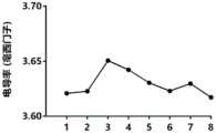
图5是本发明制备的纳米线生物传感器未经修饰时阻抗、电导率与时间的曲线。Fig. 5 is the curve of impedance, conductivity and time when the nanowire biosensor prepared by the present invention is not modified.
图6是本发明制备的纳米线生物传感器经过修饰后,阻抗、电导率和时间的曲线。Fig. 6 is the curve of impedance, conductivity and time after the nanowire biosensor prepared by the present invention is modified.
图7是本发明制备的纳米线生物传感器每步操作后阻抗的变化曲线。Fig. 7 is the change curve of impedance after each operation of the nanowire biosensor prepared by the present invention.
图8是本发明制备的纳米线生物传感器每步操作后电导率的变化曲线。Fig. 8 is the change curve of the conductivity of the nanowire biosensor prepared by the present invention after each step of operation.
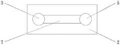
图1-图4中,1是硅基底,2是引流块,3是第一通孔,4是信号采集电极,5是第二通孔,6是金属纳米线,7是引流块底部通道,8是探针,9是对齐标志,10是绝缘层,11是导线。In Figures 1-4, 1 is a silicon substrate, 2 is a drain block, 3 is a first through hole, 4 is a signal acquisition electrode, 5 is a second through hole, 6 is a metal nanowire, and 7 is the bottom channel of the drainage block, 8 is a probe, 9 is an alignment mark, 10 is an insulating layer, and 11 is a wire.
具体实施方式Detailed ways
本发明提出的纳米线生物传感器的制备方法,其制备的纳米线生物传感器的结构如图1和图2所示,制备方法有两种,其中:For the preparation method of the nanowire biosensor proposed by the present invention, the structure of the prepared nanowire biosensor is shown in Figure 1 and Figure 2, and there are two preparation methods, wherein:
第一种制备方法包括以下步骤:The first preparation method includes the following steps:
(1)制备硅基底1:(1) Preparation of silicon substrate 1:
(1-1)将硅片先后用丙酮和异丙醇反复冲洗,用氮气吹干表面;(1-1) Rinse the silicon wafer repeatedly with acetone and isopropanol successively, and dry the surface with nitrogen;
(1-2)将干燥后的硅片放入氧化炉中,在硅片表面生长二氧化硅绝缘层,得到硅基底,二氧化硅绝缘层的厚度为100-1000纳米,本发明的一个实施例中为500纳米;(1-2) Put the dried silicon wafer into an oxidation furnace, and grow a silicon dioxide insulating layer on the surface of the silicon wafer to obtain a silicon substrate. The thickness of the silicon dioxide insulating layer is 100-1000 nanometers. One implementation of the present invention In the example, it is 500 nanometers;
(2)在步骤(1)的硅基底1上制备信号采集电极4和金属纳米线6,包括以下步骤:(2) preparing the
(2-1)在铬板上采用制版(例如利用直写式光刻设备)方法,制备得到带有对齐标志和信号采集电极的掩模铬板,备用;(2-1) Using the method of plate making (for example, using direct-write lithography equipment) on the chrome plate to prepare a mask chrome plate with alignment marks and signal collection electrodes, for use;
(2-2)将步骤(1)的硅基底1先后用丙酮和异丙醇反复冲洗三次,用氮气吹干表面,再放置于100-120℃的热板上保持1-2分钟,使硅基底1完全干燥;(2-2) The
(2-3)将干燥后的硅基底1置于匀胶机上,在硅基底1的表面旋涂电子束胶,在硅基底1的表面形成300-400纳米厚的电子束胶薄层,本发明的一个实施例中使用的电子束胶为聚甲基丙烯酸甲酯;(2-3) Place the dried
(2-4)采用电子束曝光方法,本发明的一个实施例中使用的加速电压为30keV、曝光时间为1分钟,在步骤(2-3)旋涂了电子束胶的硅基底的中央位置和对齐标志9位置上,曝光出宽度为100-500纳米、长度为50-200微米的纳米线6和对齐标志9,本发明的一个实施例中为200纳米宽、200微米长,将电子束曝光后的硅基底放入电子束显影液中将被曝光部分的电子束胶去除,在硅基底1表面得到纳米线槽和对齐标志槽,用去离子水清洗,氮气吹干;(2-4) Using the electron beam exposure method, the accelerating voltage used in one embodiment of the present invention is 30keV, and the exposure time is 1 minute, and in step (2-3), the electron beam gel is spin-coated at the central position of the silicon substrate On the position of the
(2-5)采用磁控溅射的方法,向步骤(2-4)的表面带有纳米线槽和对齐标志槽的硅基底上溅射5-20纳米厚的金属连接层,本发明的一个实施例中溅射了5纳米厚的金属铬,再溅射5-300纳米厚的金属传感层,本发明的一个实施例中溅射了100纳米厚的金属金,在硅基底表面制备得到金属纳米线和对齐标志,使用丙酮和超声结合的方式进行清洗,将硅基底表面未被曝光部分的电子束胶与金属剥离,用去离子水冲洗,氮气吹干,在100-120℃的热板上保持90秒,本发明的一个实施例中使用120℃,完全干燥;(2-5) Using the method of magnetron sputtering, sputtering a metal connection layer with a thickness of 5-20 nanometers on the silicon substrate with nanowire grooves and alignment mark grooves on the surface of step (2-4). In one embodiment, metal chrome with a thickness of 5 nanometers is sputtered, and then a metal sensing layer with a thickness of 5-300 nanometers is sputtered. The metal nanowires and alignment marks were obtained, cleaned by a combination of acetone and ultrasound, the electron beam glue on the unexposed part of the silicon substrate surface was peeled off from the metal, rinsed with deionized water, dried with nitrogen, and dried at 100-120 ° C. Keep it on the hot plate for 90 seconds, in one embodiment of the present invention, use 120°C, completely dry;
(2-6)将步骤(2-5)的带有金属纳米线6和对齐标志9的硅基底1置于匀胶机上,旋涂光刻胶(该光刻胶为负胶),在硅基底1表面形成1.3-1.5微米厚的光刻胶薄层;本发明的一个实施例中使用4340光刻胶,先以100转每分钟旋涂10秒钟,然后以4000转每分钟旋涂40秒;(2-6) The
(2-7)将步骤(2-6)的带有旋涂光刻胶的硅基底放置于光刻机上,将步骤(2-1)信号采集电极的掩模铬板放置涂有光刻胶的硅基底1上方,使硅基底1上的对齐标志9与信号采集电极4的掩模铬板上的对齐标志对齐后,并使硅基底1与信号采集电极4的掩模铬板相互贴合,采用光刻方法,从信号采集电极4的掩模铬板的上方进行光刻,再放入显影液中,将被未曝光部分的光刻胶去除,在硅基底1表面制备得到信号采集电极槽,用去离子水清洗,氮气吹干;(2-7) Place the silicon substrate with spin-coating photoresist in step (2-6) on the photolithography machine, and place the mask chrome plate of the signal collecting electrode in step (2-1) on the silicon substrate coated with photoresist Above the
(2-8)采用磁控溅射方法,对带有信号采集电极槽的硅基底表面进行磁控溅射,先溅射5-20纳米厚的金属连接层,再溅射5-300纳米厚的金属传感层,本发明的一个实施例中溅射了5纳米厚的金属连接层铬,再溅射100纳米厚的金属传感层金,采用丙酮和超声结合的方法进行清洗,将被曝光部分的光刻胶与金属剥离,用去离子水冲洗,氮气吹干,在硅基底1上制备得到信号采集电极4和金属纳米线6;(2-8) Using the magnetron sputtering method, perform magnetron sputtering on the surface of the silicon substrate with the signal collecting electrode groove, first sputter a metal connection layer with a thickness of 5-20 nanometers, and then sputter a thickness of 5-300 nanometers. In an embodiment of the present invention, a metal connection layer of chromium with a thickness of 5 nanometers is sputtered, and then a metal sensing layer of gold with a thickness of 100 nanometers is sputtered. The photoresist of the exposed part is peeled off from the metal, rinsed with deionized water, and blown dry with nitrogen, and the
(3)制备一个引流块2,其结构如图3所示,在引流块2中加工第一通孔3和第二通孔5,引流块1的底部加工凹槽,使凹槽的宽度与步骤(2)的金属纳米线的长度相等,凹槽的长度为4-6毫米,凹槽的深度为50-200微米,使该凹槽成为第一通孔3与第二通孔5之间的底部通道7,本发明的一个实施例中为5毫米,本发明实施例中为50微米;(3) Prepare a
(4)将步骤(3)的引流块2的底部与步骤(2)的硅基底1相对固定,使引流块2的底部通道7的长度方向与纳米线6的长度方向相互垂直,并完全覆盖纳米线6,图5所示为经过步骤(4)制备出的纳米线生物传感器,使磷酸缓冲盐溶液充满第一通孔3、底部通道7和第二通孔5后,通过两个信号采集电极4测量出的阻抗、电导率与时间的曲线。(4) The bottom of the
(5)在步骤(4)的纳米线6上连接探针8,包括以下步骤:(5) connecting the
(5-1)向引流块2的第一通孔3中通入溶于磷酸缓冲盐溶液的生物素修饰的牛血清蛋白溶液,生物素修饰的牛血清蛋白溶液的质量体积浓度为200微克/毫升,使生物素修饰的牛血清蛋白溶液充满第一通孔3、底部通道7和第二通孔5,使生物素修饰的牛血清蛋白溶液在底部通道7中室温下停留2小时,向引流块2的第一通孔3中通入磷酸缓冲盐溶液,使生物素修饰的牛血清蛋白溶液从第二通孔5中流出;(5-1) Pass the biotin-modified bovine serum albumin solution dissolved in phosphate buffered saline into the first through
(5-2)向引流块2的第一通孔3中通入溶于磷酸缓冲盐溶液的链霉亲和素溶液,溶于磷酸缓冲盐溶液的链霉亲和素溶液的质量体积浓度为100微克/毫升,使溶于磷酸缓冲盐溶液的链霉亲和素溶液充满第一通孔3、底部通道7和第二通孔5,溶于磷酸缓冲盐溶液的链霉亲和素溶液在底部通道7中37℃下停留1小时,向引流块2的第一通孔3中通入磷酸缓冲盐溶液,使溶于磷酸缓冲盐溶液的链霉亲和素溶液从引流块2的第二通孔5中流出;(5-2) Pass the streptavidin solution dissolved in the phosphate buffered saline solution into the first through
(5-3)向引流块2的第一通孔3中通入溶于磷酸缓冲盐溶液的生物素修饰的探针溶液,探针溶液的摩尔浓度为1微摩/毫升,使探针溶液充满第一通孔3、底部通道7和第二通孔5,在室温下停留1小时,向引流块2的第一通孔3中通入磷酸缓冲盐溶液,使探针溶液从引流块2的第二通孔5中流出,此时探针8连接上纳米线6,得到纳米线生物传感器。图6为经过步骤(5)修饰完成的纳米线生物传感器,使磷酸缓冲盐溶液充满第一通孔3、底部通道7和第二通孔5后,通过两个信号采集电极4测量出的阻抗、电导率和时间的曲线。(5-3) Pour the biotin-modified probe solution dissolved in phosphate buffered saline into the first through
或者:or:
第一种制备方法,包括以下步骤:The first preparation method includes the following steps:
(1)制备硅基底1:(1) Preparation of silicon substrate 1:
(1-1)将硅片先后用丙酮和异丙醇反复冲洗,用氮气吹干表面;(1-1) Rinse the silicon wafer repeatedly with acetone and isopropanol successively, and dry the surface with nitrogen;
(1-2)将干燥后的硅片放入氧化炉中,在硅片表面生长二氧化硅绝缘层,得到硅基底1,二氧化硅绝缘层的厚度为100-1000纳米,本发明的一个实施例中为500纳米;(1-2) Put the dried silicon wafer into an oxidation furnace, and grow a silicon dioxide insulating layer on the surface of the silicon wafer to obtain a
(2)在步骤(1)的硅基底1上制备信号采集电极4和金属纳米线6,包括以下步骤:(2) preparing the
(2-1)在铬板上采用制版(例如利用直写式光刻设备)方法,制备得到带有对齐标志和信号采集电极的掩模铬板,备用;(2-1) Using the method of plate making (for example, using direct-write lithography equipment) on the chrome plate to prepare a mask chrome plate with alignment marks and signal collection electrodes, for use;
(2-2)将步骤(1)的硅基底1先后用丙酮和异丙醇反复冲洗三次,用氮气吹干表面,再放置于100-120℃的热板上保持1-2分钟,本发明的一个实施例中使用120℃,使硅基底完全干燥;(2-2) The
(2-3)将干燥后的硅基底置于匀胶机上,在硅基底的表面旋涂电子束胶,在硅基底的表面形成300-400纳米厚的电子束胶薄层,本发明的一个实施例中使用的电子束胶为聚甲基丙烯酸甲酯;(2-3) placing the dried silicon substrate on a glue homogenizer, spin-coating electron beam glue on the surface of the silicon substrate, and forming a thin layer of electron beam glue with a thickness of 300-400 nanometers on the surface of the silicon substrate, one of the present invention The electron beam glue used in the embodiment is polymethyl methacrylate;
(2-4)采用电子束曝光方法,本发明的一个实施例中使用的加速电压为30keV、曝光时间为1分钟,在步骤(2-3)旋涂了电子束胶的硅基底的中央位置和对齐标志位置上,曝光出宽度为100-500纳米、长度为50-200微米的纳米线6和对齐标志9,本发明的一个实施例中为200纳米宽、200微米长,将电子束曝光后的硅基底放入电子束显影液中将被曝光部分的电子束胶去除,在硅基底1表面得到纳米线槽和对齐标志槽,用去离子水清洗,氮气吹干;(2-4) Using the electron beam exposure method, the accelerating voltage used in one embodiment of the present invention is 30keV, and the exposure time is 1 minute, and in step (2-3), the electron beam gel is spin-coated at the central position of the silicon substrate On the position of the alignment mark and the width of 100-500 nanometers and a length of 50-200 microns, the
(2-5)采用磁控溅射的方法,向步骤(2-4)的表面带有纳米线槽和对齐标志槽的硅基底上溅射5-20纳米厚的金属连接层,本发明的一个实施例中溅射了5纳米厚的金属钛,再溅射5-300纳米厚的金属传感层,本发明的一个实施例中溅射了100纳米厚的金属金,在硅基底1表面制备得到金属纳米线6和对齐标志9,使用丙酮和超声结合的方式进行清洗,将硅基底表面未被曝光部分的电子束胶与金属剥离,用去离子水冲洗,氮气吹干,在100-120℃的热板上保持90秒,本发明的一个实施例中使用120℃,完全干燥;(2-5) Using the method of magnetron sputtering, sputtering a metal connection layer with a thickness of 5-20 nanometers on the silicon substrate with nanowire grooves and alignment mark grooves on the surface of step (2-4). In one embodiment, metal titanium with a thickness of 5 nanometers is sputtered, and then a metal sensing layer with a thickness of 5-300 nanometers is sputtered. The
(2-6)将步骤(2-5)的带有金属纳米线6和对齐标志9的硅基底1置于匀胶机上,旋涂光刻胶(该光刻胶为负胶),在硅基底1表面形成1.3-1.5微米厚的光刻胶薄层;本发明的一个实施例中使用4340光刻胶,先以100转每分钟旋涂10秒钟,然后以4000转每分钟旋涂40秒;(2-6) The
(2-7)将步骤(2-6)的带有旋涂光刻胶的硅基底放置于光刻机上,将步骤(2-1)信号采集电极的掩模铬板放置涂有光刻胶的硅基底上方,使硅基底1上的对齐标志9与信号采集电极的掩模铬板上的对齐标志对齐后,并使硅基底1与信号采集电极的掩模铬板相互贴合,采用光刻方法,从信号采集电极的掩模铬板的上方进行光刻,再放入显影液中,将被未曝光部分的光刻胶去除,在硅基底1表面制备得到信号采集电极槽,用去离子水清洗,氮气吹干;(2-7) Place the silicon substrate with spin-coating photoresist in step (2-6) on the photolithography machine, and place the mask chrome plate of the signal collecting electrode in step (2-1) on the silicon substrate coated with photoresist Above the substrate, after aligning the
(2-8)采用磁控溅射方法,对带有信号采集电极槽的硅基底表面进行磁控溅射,先溅射5-20纳米厚的金属连接层,再溅射5-300纳米厚的金属传感层,本发明的一个实施例中溅射了5纳米厚的金属连接层钛,再溅射100纳米厚的金属传感层金,采用丙酮和超声结合的方法进行清洗,将被曝光部分的光刻胶与金属剥离,用去离子水冲洗,氮气吹干,在硅基底上制备得到信号采集电极4和金属纳米线6;(2-8) Using the magnetron sputtering method, perform magnetron sputtering on the surface of the silicon substrate with the signal collecting electrode groove, first sputter a metal connection layer with a thickness of 5-20 nanometers, and then sputter a thickness of 5-300 nanometers. In an embodiment of the present invention, a metal connection layer of titanium with a thickness of 5 nanometers is sputtered, and then a metal sensing layer of gold with a thickness of 100 nanometers is sputtered. The photoresist of the exposed part is peeled off from the metal, rinsed with deionized water, and blown dry with nitrogen, and the
(3)制备一个引流块2,在引流块2中加工第一通孔3和第二通孔5,引流块2的底部加工凹槽,使凹槽的宽度与步骤(2)的金属纳米线的长度相等,凹槽的长度为4-6毫米,凹槽的深度为50-200微米,使该凹槽成为第一通孔与第二通孔之间的底部通道7,本发明的一个实施例中为5毫米,本发明实施例中为50微米;(3) Prepare a
(4)将步骤(3)的引流块2的底部与步骤(2)的硅基底1相对固定,使引流块2的底部通道7的长度方向与纳米线6的长度方向相互垂直,并完全覆盖纳米线6;(4) The bottom of the
(5)在步骤(4)的纳米线6上连接探针8,包括以下步骤:(5) connecting the
(5-1)向引流块2的第一通孔3中通入溶于纯乙醇的11-巯基十一烷酸溶液,溶于纯乙醇的11-巯基十一烷酸溶液的摩尔浓度为1毫摩尔/升,使溶于纯乙醇的11-巯基十一烷酸溶液充满第一通孔3、底部通道7和第二通孔5,溶于纯乙醇的11-巯基十一烷酸溶液在底部通道7中室温下停留1小时,向引流块2的第一通孔3中通入纯乙醇,使溶于纯乙醇的11-巯基十一烷酸从引流块2的第二通孔5中流出;(5-1) Pour 11-mercaptoundecanoic acid solution dissolved in pure ethanol into the first through
(5-2)向引流块2的第一通孔3中通入摩尔浓度为50毫摩尔/升、pH=5.0的2-(N-吗啉)乙磺酸溶液,该溶液中包含摩尔浓度为100毫摩尔/升的N-乙基-N′-(3-二甲基氨基丙基)碳二亚胺盐酸盐(EDC)和摩尔浓度为50毫摩尔/升的N-羟基丁二酰亚胺(NHS),使该溶液充满第一通孔3、底部通道7和第二通孔5,在底部通道7中室温下停留30分钟;(5-2) Pour a 2-(N-morpholine)ethanesulfonic acid solution with a molar concentration of 50 mmol/L and pH=5.0 into the first through
(5-3)向引流块2的第一通孔3中通入溶于磷酸缓冲盐溶液的链霉亲和素溶液,溶于磷酸缓冲盐溶液的链霉亲和素溶液的质量体积浓度为100微克/毫升,使该溶液充满第一通孔3、底部通道7和第二通孔5,在底部通道7中室温下停留1小时,向引流块2的第一通孔3中通入磷酸缓冲盐溶液,使溶于磷酸缓冲盐溶液的链霉亲和素溶液从引流块2的第二通孔5中流出;(5-3) Pass the streptavidin solution dissolved in the phosphate buffered saline solution into the first through
(5-4)向引流块2的第一通孔3中通入溶于去离子水的甘氨酸溶液,溶于去离子水的甘氨酸溶液的摩尔浓度为1摩尔/升,使该溶液充满第一通孔3、底部通道7和第二通孔5,在底部通道7中室温下停留20分钟,向引流块2的第一通孔3中通入去离子水,使溶于去离子水的甘氨酸溶液从引流块2的第二通孔5中流出;(5-4) Pour a glycine solution dissolved in deionized water into the first through
(5-5)向引流块2的第一通孔3中通入溶于磷酸缓冲盐溶液的生物素修饰的探针溶液,探针溶液的摩尔浓度为1微摩尔/升,使探针溶液充满第一通孔3、底部通道7和第二通孔5,探针溶液在底部通道7中室温下停留1小时,向引流块2的第一通孔3中通入磷酸缓冲盐溶液,使探针溶液从引流块2的第二通孔5中流出,此时探针8连接上纳米线6,得到纳米线生物传感器。(5-5) Pass the biotin-modified probe solution dissolved in phosphate buffered saline into the first through
本发明的第二种方法制备的纳米线生物传感器,其结构如图4所示,第二种制备方法包括以下步骤:The structure of the nanowire biosensor prepared by the second method of the present invention is shown in Figure 4, and the second preparation method includes the following steps:
(1)制备硅基底1:(1) Preparation of silicon substrate 1:
(1-1)将硅片先后用丙酮和异丙醇反复冲洗,用氮气吹干表面;(1-1) Rinse the silicon wafer repeatedly with acetone and isopropanol successively, and dry the surface with nitrogen;
(1-2)将干燥后的硅片放入氧化炉中,在硅片表面生长二氧化硅绝缘层,得到硅基底1,二氧化硅绝缘层的厚度为100-1000纳米,本发明的一个实施例中为500纳米;(1-2) Put the dried silicon wafer into an oxidation furnace, and grow a silicon dioxide insulating layer on the surface of the silicon wafer to obtain a
(2)在步骤(1)的硅基底上制备信号采集电极4和金属纳米线6,包括以下步骤:(2) preparing the
(2-1)在铬板上采用制版(例如利用直写式光刻设备)方法,制备得到带有对齐标志和信号采集电极的掩模铬板,备用;(2-1) Using the method of plate making (for example, using direct-write lithography equipment) on the chrome plate to prepare a mask chrome plate with alignment marks and signal collection electrodes, for use;
(2-2)将步骤(1)的硅基底1先后用丙酮和异丙醇反复冲洗三次,用氮气吹干表面,再放置于100-120℃的热板上保持1-2分钟,本发明的一个实施例中使用120℃,使硅基底完全干燥;(2-2) The
(2-3)将干燥后的硅基底1置于匀胶机上,在硅基底1的表面旋涂电子束胶,在硅基底1的表面形成300-400纳米厚的电子束胶薄层,本发明的一个实施例中使用的电子束胶为聚甲基丙烯酸甲酯;(2-3) Place the dried
(2-4)采用电子束曝光方法,本发明的一个实施例中使用的加速电压为30keV、曝光时间为1分钟,在步骤(2-3)旋涂了电子束胶的硅基底的中央位置和对齐标志位置上,曝光出宽度为100-500纳米、长度为50-200微米的纳米线和对齐标志,本发明的一个实施例中为200纳米宽、200微米长,将电子束曝光后的硅基底放入电子束显影液中将被曝光部分的电子束胶去除,在硅基底表面得到纳米线槽和对齐标志槽,用去离子水清洗,氮气吹干;(2-4) Using the electron beam exposure method, the accelerating voltage used in one embodiment of the present invention is 30keV, and the exposure time is 1 minute, and in step (2-3), the electron beam gel is spin-coated at the central position of the silicon substrate On the position of the alignment mark and the width of 100-500 nanometers and the length of 50-200 microns, nanowires and alignment marks, which are 200 nanometers wide and 200 microns long in one embodiment of the present invention, are exposed. The silicon substrate is placed in an electron beam developer to remove the electron beam glue from the exposed part, and nanowire grooves and alignment mark grooves are obtained on the surface of the silicon substrate, rinsed with deionized water, and dried with nitrogen;
(2-5)采用磁控溅射的方法,向步骤(2-4)的表面带有纳米线槽和对齐标志槽的硅基底上溅射5-20纳米厚的金属连接层,本发明的一个实施例中溅射了5纳米厚的金属铬,再溅射5-300纳米厚的金属传感层,本发明的一个实施例中溅射了100纳米厚的金属铂,在硅基底1表面制备得到金属纳米线6和对齐标志9,使用丙酮和超声结合的方式进行清洗,将硅基底表面未被曝光部分的电子束胶与金属剥离,用去离子水冲洗,氮气吹干,在100-120℃的热板上保持90秒,本发明的一个实施例中使用120℃,完全干燥;(2-5) Using the method of magnetron sputtering, sputtering a metal connection layer with a thickness of 5-20 nanometers on the silicon substrate with nanowire grooves and alignment mark grooves on the surface of step (2-4). In one embodiment, metal chromium is sputtered with a thickness of 5 nanometers, and then a metal sensing layer with a thickness of 5-300 nanometers is sputtered. The
(2-6)将步骤(2-5)的带有金属纳米线6和对齐标志9的硅基底1置于匀胶机上,旋涂光刻胶(该光刻胶为负胶),在硅基底表面形成1.3-1.5微米厚的光刻胶薄层;本发明的一个实施例中使用4340光刻胶,先以100转每分钟旋涂10秒钟,然后以4000转每分钟旋涂40秒;(2-6) The
(2-7)将步骤(2-6)的带有旋涂光刻胶的硅基底放置于光刻机上,将步骤(2-1)信号采集电极的掩模铬板放置涂有光刻胶的硅基底1上方,使硅基底1上的对齐标志9与信号采集电极的掩模铬板上的对齐标志对齐后,并使硅基底1与信号采集电极的掩模铬板相互贴合,采用光刻方法,从信号采集电极的掩模铬板的上方进行光刻,再放入显影液中,将被未曝光部分的光刻胶去除,在硅基底1表面制备得到信号采集电极槽,用去离子水清洗,氮气吹干;(2-7) Place the silicon substrate with spin-coating photoresist in step (2-6) on the photolithography machine, and place the mask chrome plate of the signal collecting electrode in step (2-1) on the silicon substrate coated with photoresist Above the
(2-8)采用磁控溅射方法,对带有信号采集电极槽的硅基底表面进行磁控溅射,先溅射5-20纳米厚的金属连接层,再溅射5-300纳米厚的金属传感层,本发明的一个实施例中溅射了5纳米厚的金属连接层铬,再溅射100纳米厚的金属传感层铂,采用丙酮和超声结合的方法进行清洗,将被曝光部分的光刻胶与金属剥离,用去离子水冲洗,氮气吹干,在硅基底1上制备得到信号采集电极4和金属纳米线6;(2-8) Using the magnetron sputtering method, perform magnetron sputtering on the surface of the silicon substrate with the signal collecting electrode groove, first sputter a metal connection layer with a thickness of 5-20 nanometers, and then sputter a thickness of 5-300 nanometers. In one embodiment of the present invention, a metal connection layer of chromium with a thickness of 5 nanometers is sputtered, and then a metal sensing layer of platinum with a thickness of 100 nanometers is sputtered. The photoresist of the exposed part is peeled off from the metal, rinsed with deionized water, and blown dry with nitrogen, and the
(3)在步骤(2)的纳米线6上连接探针8,包括以下步骤:(3) connecting the
(3-1)将两根导线11分别放置于信号采集电极4上,使用绝缘物质10覆盖放有导线的信号采集电极4,使纳米线6暴露于外部,形成一个检测单元;(3-1) two wires 11 are placed on the
(3-2)将检测单元放入溶有生物素修饰的牛血清蛋白的磷酸缓冲盐溶液中,溶有生物素修饰的牛血清蛋白的磷酸缓冲盐溶液的质量体积浓度为200微克/毫升,室温下静置2小时,取出检测单元,用磷酸缓冲盐溶液冲洗,去除检测单元表面的未反应的生物素修饰的牛血清蛋白;(3-2) Put the detection unit into the phosphate buffered saline solution dissolved with biotin-modified bovine serum albumin, and the mass volume concentration of the phosphate buffered saline solution dissolved with biotin-modified bovine serum albumin is 200 μg/ml, Let stand for 2 hours at room temperature, take out the detection unit, rinse with phosphate buffered saline, and remove the unreacted biotin-modified bovine serum albumin on the surface of the detection unit;
(3-3)将检测单元通放入溶有链霉亲和素的磷酸缓冲盐溶液中,溶有链霉亲和素的磷酸缓冲盐溶液的质量体积浓度为100微克/毫升,37℃下静置1小时,取出检测单元,用磷酸缓冲盐溶液冲洗,去除检测单元表面的未反应的链霉亲和素;(3-3) Put the detection unit into the streptavidin-dissolved phosphate-buffered saline solution, and the mass-volume concentration of the streptavidin-dissolved phosphate-buffered saline solution is 100 μg/ml. Let stand for 1 hour, take out the detection unit, rinse with phosphate buffered saline to remove unreacted streptavidin on the surface of the detection unit;
(3-4)将检测单元放入溶有生物素修饰的探针的磷酸缓冲盐溶液中,该溶液的摩尔浓度为1微摩/毫升,37℃下静置一小时,在检测单元表面暴露的纳米线连接上探针,取出检测单元,用磷酸缓冲盐溶液冲洗,去除检测单元表面的未反应探针此时探针连接上纳米线,得到纳米线生物传感器。(3-4) Put the detection unit into the phosphate buffered saline solution dissolved with the biotin-modified probe, the molar concentration of the solution is 1 μM/ml, stand at 37°C for one hour, and expose it on the surface of the detection unit The nanowire is connected to the probe, the detection unit is taken out, rinsed with a phosphate buffered saline solution, and the unreacted probe on the surface of the detection unit is removed. At this time, the probe is connected to the nanowire to obtain a nanowire biosensor.
或者:or:
第二种制备方法包括以下步骤:The second preparation method includes the following steps:
(1)制备硅基底1:(1) Preparation of silicon substrate 1:
(1-1)将硅片先后用丙酮和异丙醇反复冲洗,用氮气吹干表面;(1-1) Rinse the silicon wafer repeatedly with acetone and isopropanol successively, and dry the surface with nitrogen;
(1-2)将干燥后的硅片放入氧化炉中,在硅片表面生长二氧化硅绝缘层,得到硅基底1,二氧化硅绝缘层的厚度为100-1000纳米,本发明的一个实施例中为500纳米;(1-2) Put the dried silicon wafer into an oxidation furnace, and grow a silicon dioxide insulating layer on the surface of the silicon wafer to obtain a
(2)在步骤(1)的硅基底上制备信号采集电极4和金属纳米线6,包括以下步骤:(2) preparing the
(2-1)在铬板上采用制版(利用直写式光刻设备)方法,制备得到带有对齐标志的信号采集电极的掩模铬板,备用;(2-1) Using a plate-making method (using direct-write lithography equipment) on a chrome plate to prepare a mask chrome plate with a signal-collecting electrode with an alignment mark, for use;
(2-2)将步骤(1)的硅基底1先后用丙酮和异丙醇反复冲洗三次,用氮气吹干表面,再放置于100-120℃的热板上保持1-2分钟,本发明的一个实施例中使用120℃,使硅基底完全干燥;(2-2) The
(2-3)将干燥后的硅基底1置于匀胶机上,在硅基底1的表面旋涂电子束胶,在硅基底1的表面形成300-400纳米厚的电子束胶薄层,本发明的一个实施例中使用的电子束胶为聚甲基丙烯酸甲酯;(2-3) Place the dried
(2-4)采用电子束曝光方法,本发明的一个实施例中使用的加速电压为30keV、曝光时间为1分钟,在步骤(2-3)旋涂了电子束胶的硅基底的中央位置和对齐标志位置上,曝光出宽度为100-500纳米、长度为50-200微米的纳米线和对齐标志,本发明的一个实施例中为200纳米宽、200微米长,将电子束曝光后的硅基底放入电子束显影液中将被曝光部分的电子束胶去除,在硅基底1表面得到纳米线槽和对齐标志槽,用去离子水清洗,氮气吹干;(2-4) Using the electron beam exposure method, the accelerating voltage used in one embodiment of the present invention is 30keV, and the exposure time is 1 minute, and in step (2-3), the electron beam gel is spin-coated at the central position of the silicon substrate On the position of the alignment mark and the width of 100-500 nanometers and the length of 50-200 microns, nanowires and alignment marks, which are 200 nanometers wide and 200 microns long in one embodiment of the present invention, are exposed. The silicon substrate is put into the electron beam developer to remove the electron beam glue in the exposed part, and the nanowire groove and the alignment mark groove are obtained on the surface of the
(2-5)采用磁控溅射的方法,向步骤(2-3)的表面带有纳米线槽和对齐标志槽的硅基底上溅射5-20纳米厚的金属连接层,本发明的一个实施例中溅射了5纳米厚的金属钛,再溅射5-300纳米厚的金属传感层,本发明的一个实施例中溅射了100纳米厚的金属铂,在硅基底1表面制备得到金属纳米线6和对齐标志9,使用丙酮和超声结合的方式进行清洗,将硅基底表面未被曝光部分的电子束胶与金属剥离,用去离子水冲洗,氮气吹干,在100-120℃的热板上保持90秒,本发明的一个实施例中使用120℃,完全干燥;(2-5) Using the method of magnetron sputtering, sputter a metal connection layer with a thickness of 5-20 nanometers on the silicon substrate with nanowire grooves and alignment mark grooves on the surface of step (2-3). In one embodiment, metal titanium with a thickness of 5 nanometers is sputtered, and then a metal sensing layer with a thickness of 5-300 nanometers is sputtered. The
(2-6)将步骤(2-5)的带有金属纳米线6和对齐标志9的硅基底1置于匀胶机上,旋涂光刻胶(该光刻胶为负胶),在硅基底1表面形成1.3-1.5微米厚的光刻胶薄层;本发明的一个实施例中使用4340光刻胶,先以100转每分钟旋涂10秒钟,然后以4000转每分钟旋涂40秒;(2-6) The
(2-7)将步骤(2-6)的带有旋涂光刻胶的硅基底放置于光刻机上,将步骤(2-1)信号采集电极的掩模铬板放置涂有光刻胶的硅基底上方,使硅基底1上的对齐标志9与信号采集电极的掩模铬板上的对齐标志对齐后,并使硅基底1与信号采集电极的掩模铬板相互贴合,采用光刻方法,从信号采集电极的掩模铬板的上方进行光刻,再放入显影液中,将被未曝光部分的光刻胶去除,在硅基底1表面制备得到信号采集电极槽,用去离子水清洗,氮气吹干;(2-7) Place the silicon substrate with spin-coating photoresist in step (2-6) on the photolithography machine, and place the mask chrome plate of the signal collecting electrode in step (2-1) on the silicon substrate coated with photoresist Above the substrate, after aligning the
(2-8)采用磁控溅射方法,对带有信号采集电极槽的硅基底表面进行磁控溅射,先溅射5-20纳米厚的金属连接层,再溅射5-300纳米厚的金属传感层,本发明的一个实施例中溅射了5纳米厚的金属钛,再溅射100纳米厚的金属铂,采用丙酮和超声结合的方法进行清洗,将被曝光部分的光刻胶与金属剥离,用去离子水冲洗,氮气吹干,在硅基底上制备得到信号采集电极4和金属纳米线6;(2-8) Using the magnetron sputtering method, perform magnetron sputtering on the surface of the silicon substrate with the signal collecting electrode groove, first sputter a metal connection layer with a thickness of 5-20 nanometers, and then sputter a thickness of 5-300 nanometers. In an embodiment of the present invention, metal titanium with a thickness of 5 nanometers is sputtered, and then metal platinum with a thickness of 100 nanometers is sputtered, and the combined method of acetone and ultrasonic is used for cleaning. The glue is peeled off from the metal, rinsed with deionized water, dried with nitrogen, and prepared on the silicon substrate to obtain the
(3)在步骤(2)的纳米线6上连接探针8,包括以下步骤:(3) connecting the
(3-1)将两根导线11分别放置于信号采集电极4上,使用绝缘物质10覆盖放有导线的信号采集电极4,使纳米线6暴露于外部,形成一个检测单元;(3-1) two wires 11 are placed on the
(3-2)将检测单元放入溶有11-巯基十一烷酸的纯乙醇溶液中,溶有11-巯基十一烷酸的纯乙醇溶液的摩尔浓度为1毫摩尔/升,室温下静置1小时,取出检测单元,用纯乙醇冲洗检测单元,去除检测单元表面未反应的11-巯基十一烷酸;(3-2) Put the detection unit into the pure ethanol solution dissolved in 11-mercaptoundecanoic acid, the molar concentration of the pure ethanol solution dissolved in 11-mercaptoundecanoic acid is 1 mmol/L, and at room temperature Let stand for 1 hour, take out the detection unit, rinse the detection unit with pure ethanol, and remove the unreacted 11-mercaptoundecanoic acid on the surface of the detection unit;
(3-3)将检测单元放入摩尔浓度为50毫摩尔/升、pH=5.0的2-(N-吗啉)乙磺酸(MES)中,其中包含摩尔浓度为100毫摩尔/升的N-乙基-N′-(3-二甲基氨基丙基)碳二亚胺盐酸盐(EDC)和摩尔浓度为50毫摩尔/升的N-羟基丁二酰亚胺(NHS),室温下静置30分钟,取出检测单元;(3-3) Put the detection unit into 2-(N-morpholine)ethanesulfonic acid (MES) with a molar concentration of 50 mmol/L and pH=5.0, which contains a molar concentration of 100 mmol/L. N-ethyl-N'-(3-dimethylaminopropyl)carbodiimide hydrochloride (EDC) and N-hydroxysuccinimide (NHS) at a molar concentration of 50 mmol/L, Let stand for 30 minutes at room temperature, and take out the detection unit;
(3-4)将检测单元快速放入溶有链霉亲和素的磷酸缓冲盐溶液中,该溶液的质量体积浓度为100微克/毫升,室温下静置1小时,取出检测单元,用磷酸缓冲盐溶液冲洗检测单元,去除检测单元表面未反应的链霉亲和素;(3-4) Quickly put the detection unit into the streptavidin-dissolved phosphate buffered saline solution, the mass volume concentration of the solution is 100 μg/ml, stand at room temperature for 1 hour, take out the detection unit, use phosphoric acid Rinse the detection unit with buffered saline solution to remove unreacted streptavidin on the surface of the detection unit;
(3-5)将检测单元放入摩尔浓度为1摩尔/升的溶有甘氨酸的去离子水中,室温下静置20分钟,取出检测单元,用去离子水冲洗检测单元,去除检测单元表面未反应的甘氨酸;(3-5) Put the detection unit into deionized water with glycine dissolved in a molar concentration of 1 mol/L, leave it to stand for 20 minutes at room temperature, take out the detection unit, rinse the detection unit with deionized water, and remove the surface of the detection unit. reacted glycine;
(3-6)将检测单元放入摩尔浓度为1微摩/毫升的溶有生物素修饰的探针的磷酸缓冲盐溶液中,37℃下静置一小时,在检测单元表面暴露的纳米线连接上探针,取出检测单元,用磷酸缓冲盐溶液冲洗检测单元,去除检测单元表面未反应的探针,得到纳米线生物传感器。(3-6) Put the detection unit into a phosphate buffered saline solution containing a biotin-modified probe with a molar concentration of 1 μM/ml, and let it stand at 37° C. for one hour to expose the nanowires on the surface of the detection unit. Connect the probe, take out the detection unit, rinse the detection unit with a phosphate buffered saline solution, remove the unreacted probe on the surface of the detection unit, and obtain a nanowire biosensor.
上述第一种方法制备的纳米线生物传感器的应用,包括以下步骤:The application of the nanowire biosensor prepared by the first method above includes the following steps:
(1)向纳米线生物传感器中引流块2的第一通孔3中通入磷酸缓冲盐溶液(PBS),使磷酸缓冲盐溶液充满第一通孔3、底部通道7和第二通孔5,使用电化学工作站连接信号采集纳米线生物传感器上信号采集电极4的第一电压-电流曲线和电化学阻抗谱曲线;(1) Pour phosphate buffered saline (PBS) into the first through
(2)向引流块2的第一通孔3中通入与纳米线生物传感器中探针相互补的目标序列,静置10分钟后,采集纳米线生物传感器上信号采集电极4的第二电压-电流曲线和电化学阻抗谱曲线;(2) Passing a target sequence complementary to the probe in the nanowire biosensor into the first through
(3)对纳米线生物传感器上的信号采集电极4施加一个1-1.5伏的直流电压,施加时间为60-90秒,本发明的一个实施例中使用1.2伏,持续60秒,使目标序列从纳米线6上释放,并从引流块2的第二通孔5中流出,采集信号采集电极4的第三电压-电流曲线和电化学阻抗谱曲线;图7所示为第一种方法制备的纳米线生物传感器经过每步修饰操作和上述(1)-(3)每步操作后,通过两个信号采集电极4测量出的阻抗的变化曲线。通过图8所示为第一种方法制备的纳米线生物传感器经过每步修饰操作和上述(1)-(3)每步操作后,通过两个信号采集电极4测量出的电导率的变化曲线。图7和图8中,1代表纳米线生物传感器初始状态时通过两个信号采集电极4测量出的数据,2代表纳米线生物传感器经过生物素修饰的牛血清蛋白修饰后,通过两个信号采集电极4测量出的数据,3代表纳米线生物传感器经过链霉亲和素修饰后,通过两个信号采集电极4测量出的数据,4代表纳米线生物传感器经过生物素修饰的探针修饰后,通过两个信号采集电极4测量出的数据,5代表向纳米线生物传感器中通入1飞摩尔目标序列静置15分钟,通入磷酸缓冲盐溶液后,通过两个信号采集电极4测量出的数据,6代表向纳米线生物传感器中通入1皮摩尔目标序列静置15分钟,通入磷酸缓冲盐溶液后,通过两个信号采集电极4测量出的数据,7代表经过对两个信号采集电极4施加1.1伏的直流电压,施加时间为1分钟后,通过两个信号采集电极4测量出的数据,8代表向纳米线生物传感器中通入1皮摩尔目标序列静置15分钟,通入磷酸缓冲盐溶液后,通过两个信号采集电极4测量出的数据。(3) Apply a DC voltage of 1-1.5 volts to the
(4)向引流块2的第一通孔3中通入与纳米线生物传感器中探针相互补的目标序列,静置10分钟后,采集纳米线生物传感器上信号采集电极4的第四电压-电流曲线和电化学阻抗谱曲线;(4) Pass the target sequence complementary to the probe in the nanowire biosensor into the first through
(5)将上述第一电压-电流曲线和电化学阻抗谱曲线、第二电压-电流曲线和电化学阻抗谱曲线、第三电压-电流曲线和电化学阻抗谱曲线和第四电压-电流曲线和电化学阻抗谱曲线进行对比,实现核酸检测;(5) Combine the above-mentioned first voltage-current curve and electrochemical impedance spectrum curve, second voltage-current curve and electrochemical impedance spectrum curve, third voltage-current curve and electrochemical impedance spectrum curve and fourth voltage-current curve Compare with electrochemical impedance spectroscopy curve to realize nucleic acid detection;
(6)重复步骤(1)-(5),进行目标核酸序列的多次重复检测。(6) Repeat steps (1)-(5) to perform multiple repeated detection of the target nucleic acid sequence.
上述第二种方法制备的纳米线生物传感器的应用,包括以下步骤:The application of the nanowire biosensor prepared by the second method above includes the following steps:
(1)将纳米线生物传感器放入到细胞培养基中,采集纳米线生物传感器上信号采集电极4的第一电压-电流曲线和电化学阻抗谱曲线;(1) Put the nanowire biosensor into the cell culture medium, and collect the first voltage-current curve and the electrochemical impedance spectrum curve of the
(2)根据设定的时间间隔,采集纳米线生物传感器上信号采集电极的多个电压-电流曲线和电化学阻抗谱曲线,记录多个电压-电流曲线和电化学阻抗谱曲线,通过对多个曲线进行对比,实现目标核酸序列的检测;(2) According to the set time interval, collect multiple voltage-current curves and electrochemical impedance spectrum curves of the signal collecting electrodes on the nanowire biosensor, record multiple voltage-current curves and electrochemical impedance spectrum curves, Compare each curve to detect the target nucleic acid sequence;
(3)对纳米线生物传感器上的信号采集电极施加一个1-1.5伏的直流电压,施加时间为60-90秒,使目标序列从纳米线上释放;(3) applying a DC voltage of 1-1.5 volts to the signal collection electrode on the nanowire biosensor for 60-90 seconds to release the target sequence from the nanowire;
(4)重复步骤(1)-(3),进行目标核酸序列的多次重复检测。(4) Repeat steps (1)-(3) to perform multiple repeated detection of the target nucleic acid sequence.
本发明方法的原理是,已有技术中核酸解链方法包含升温、改变pH值和使用解旋酶等,本发明为了在不添加额外试剂的前提下实现核酸解链,升温为最佳方案。金属纳米线符合上述需求,因此选择了金属纳米线作为传感器的核心部件。金属纳米线的制备采用双层方式,下层为金属连接层,常用金属为铬、钛等,上层为金属传感层,常用金属为金、铂等。上述金属都有优异的理化性质,与大部分的化学物都不会发生化学反应,具有良好的稳定性。金、铂金纳米结构都是电化学应用中优秀的纳米电极候选者,可以应用于压力传感器、DNA检测传感器等。同时,金属纳米线可以提供高电流密度、高信噪比和低双电子层电容,十分适合制作成传感器。The principle of the method of the present invention is that the nucleic acid melting method in the prior art includes heating, changing the pH value and using a helicase. Metal nanowires meet the above requirements, so metal nanowires are selected as the core components of the sensor. The preparation of metal nanowires adopts a double-layer method, the lower layer is a metal connection layer, the commonly used metals are chromium, titanium, etc., and the upper layer is a metal sensing layer, and the commonly used metals are gold, platinum, etc. The above metals have excellent physical and chemical properties, do not chemically react with most chemicals, and have good stability. Gold and platinum nanostructures are both excellent nanoelectrode candidates for electrochemical applications, which can be applied to pressure sensors, DNA detection sensors, etc. At the same time, metal nanowires can provide high current density, high signal-to-noise ratio and low double electronic layer capacitance, which are very suitable for making sensors.
由于金属纳米线优异的导电性能与热传导性能,其宽度为纳米级别,长度为微米级别,当给金属纳米线两端施加一定时间的固定电压后,可在金属纳米线表面产生一定的温度,可用来对捕获到的生物标志物进行解链与原位释放,与此同时也要保证金属纳米线表面上所进行的修饰不会被破坏。Due to the excellent electrical conductivity and thermal conductivity of metal nanowires, its width is nanometer level and its length is micrometer level. To unzip and release the captured biomarkers in situ, at the same time, it is necessary to ensure that the modification on the surface of the metal nanowires will not be destroyed.
本发明中所使用的修饰体系基于亲和素与生物素的结合。通过文献调研可知,腺嘌呤与胸腺嘧啶的键能为8kJ/mol或1.9kcal/mol,鸟嘌呤与胞嘧啶的键能为13kJ/mol或3.1kcal/mol。而亲和素结合生物素的亲和常数为普通抗原-抗体反应的百万倍,两者形成复合物的解离常数很小,且100℃时不会变性,呈现为不可逆反应性,而且酸、碱、变性剂、蛋白溶解酶以及有机溶剂均不影响其结合。The modification system used in the present invention is based on the combination of avidin and biotin. According to literature research, the bond energy between adenine and thymine is 8kJ/mol or 1.9kcal/mol, and the bond energy between guanine and cytosine is 13kJ/mol or 3.1kcal/mol. The affinity constant of avidin binding to biotin is a million times that of the common antigen-antibody reaction, the dissociation constant of the complex formed by the two is very small, and it will not be denatured at 100 °C, showing irreversible reactivity, and acid , alkalis, denaturants, proteolytic enzymes and organic solvents do not affect their binding.
因此在金属纳米线通过对纳米线施加电脉冲信号产生大量热的过程中,亲和素和生物素结合的稳定性远远高于DNA双链与抗原-抗体反应,因此可以通过精确控制金属纳米线表面加热实现对生物标志物的解链与原位释放。以用于对生物标志物含量的动态实时检测,来反应病人的身体健康情况。Therefore, in the process of metal nanowires generating a large amount of heat by applying electrical pulse signals to the nanowires, the binding stability of avidin and biotin is much higher than that of DNA double-strands and antigen-antibody reaction. Heating of the wire surface enables melting and in situ release of the biomarkers. It is used for dynamic real-time detection of biomarker content to reflect the patient's physical health.
Claims (7)
Translated fromChinesePriority Applications (2)
| Application Number | Priority Date | Filing Date | Title |
|---|---|---|---|
| CN201911370420.8ACN111175347B (en) | 2019-12-26 | 2019-12-26 | A kind of preparation method of nanowire biosensor and its application |
| PCT/CN2020/114822WO2021128956A1 (en) | 2019-12-26 | 2020-09-11 | Nanowire biosensor, preparation method therefor and application thereof |
Applications Claiming Priority (1)
| Application Number | Priority Date | Filing Date | Title |
|---|---|---|---|
| CN201911370420.8ACN111175347B (en) | 2019-12-26 | 2019-12-26 | A kind of preparation method of nanowire biosensor and its application |
Publications (2)
| Publication Number | Publication Date |
|---|---|
| CN111175347A CN111175347A (en) | 2020-05-19 |
| CN111175347Btrue CN111175347B (en) | 2020-12-29 |
Family
ID=70652181
Family Applications (1)
| Application Number | Title | Priority Date | Filing Date |
|---|---|---|---|
| CN201911370420.8AActiveCN111175347B (en) | 2019-12-26 | 2019-12-26 | A kind of preparation method of nanowire biosensor and its application |
Country Status (2)
| Country | Link |
|---|---|
| CN (1) | CN111175347B (en) |
| WO (1) | WO2021128956A1 (en) |
Families Citing this family (4)
| Publication number | Priority date | Publication date | Assignee | Title |
|---|---|---|---|---|
| CN111175347B (en)* | 2019-12-26 | 2020-12-29 | 清华大学 | A kind of preparation method of nanowire biosensor and its application |
| CN114199969B (en)* | 2021-12-03 | 2023-04-28 | 清华大学 | Nano electrode biosensor based on nucleic acid aptamer and application thereof |
| CN114527180B (en)* | 2022-01-25 | 2022-12-20 | 清华大学 | Metal nanowire biosensor and preparation method and application thereof |
| CN115181657A (en)* | 2022-08-18 | 2022-10-14 | 中国科学院上海微系统与信息技术研究所 | A device and method for monitoring nucleic acid amplification process in situ |
Citations (9)
| Publication number | Priority date | Publication date | Assignee | Title |
|---|---|---|---|---|
| JPS56104241A (en)* | 1980-01-24 | 1981-08-19 | Nec Corp | Gas sensing element |
| CN1844907A (en)* | 2006-05-09 | 2006-10-11 | 北京大学 | Preparation method of biosensor based on carbon nanotube |
| CN101776637A (en)* | 2009-01-13 | 2010-07-14 | 国家纳米科学中心 | Photoelectrochemistry biosensor and preparation method thereof |
| CN102375007A (en)* | 2010-08-13 | 2012-03-14 | 北京大学 | Molecular biosensor and method of single-molecule detection of DNA or protein using the same |
| CN102628827A (en)* | 2012-04-10 | 2012-08-08 | 凯晶生物科技(苏州)有限公司 | DNA (Deoxyribonucleic Acid) electrochemical sensor based on MOSFET (Metal-Oxide -Semiconductor Field Effect Transistor) structure and manufacturing method thereof |
| CN106206296A (en)* | 2016-08-08 | 2016-12-07 | 北京大学 | A kind of integrated approach of the nanowire biosensor of vertical-channel |
| CN107807239A (en)* | 2017-10-26 | 2018-03-16 | 无锡市人民医院 | A kind of hypersensitivity biology sensor method of preparation and use based on silicon nanobelt |
| CN108700535A (en)* | 2015-12-23 | 2018-10-23 | 加利福尼亚大学董事会 | Nanosensors for nucleic acid detection and identification |
| CN110501354A (en)* | 2019-08-28 | 2019-11-26 | 济南大学 | A kind of biosensor, its preparation method and application |
Family Cites Families (11)
| Publication number | Priority date | Publication date | Assignee | Title |
|---|---|---|---|---|
| WO2004051219A2 (en)* | 2002-11-27 | 2004-06-17 | Molecular Nanosystems, Inc. | Nanotube chemical sensor based on work function of electrodes |
| KR100874026B1 (en)* | 2006-04-04 | 2008-12-17 | 재단법인서울대학교산학협력재단 | Biosensor using nanowires and its manufacturing method |
| KR20090065272A (en)* | 2007-12-17 | 2009-06-22 | 한국전자통신연구원 | Biosensor and its manufacturing method |
| KR20090065124A (en)* | 2007-12-17 | 2009-06-22 | 한국전자통신연구원 | Biosensor using silicon nanowires and its manufacturing method |
| JP6413222B2 (en)* | 2013-10-23 | 2018-10-31 | 大日本印刷株式会社 | Conductive material for biosensor and biosensor |
| JP6544461B2 (en)* | 2018-04-23 | 2019-07-17 | 大日本印刷株式会社 | Electrically conductive material for biosensors and biosensors |
| CN108957007B (en)* | 2018-07-24 | 2021-08-17 | 无锡市人民医院 | A biosensor combining dialysis device and silicon nanowire field effect tube |
| CN111380929B (en)* | 2018-12-27 | 2023-01-06 | 有研工程技术研究院有限公司 | A silicon nanowire cell sensor based on FinFET fabrication process |
| CN110116987A (en)* | 2019-03-15 | 2019-08-13 | 大连理工大学 | A kind of semiconductor nanowires sensor |
| JP6702488B2 (en)* | 2019-06-19 | 2020-06-03 | 大日本印刷株式会社 | Conductive material for biosensor and biosensor |
| CN111175347B (en)* | 2019-12-26 | 2020-12-29 | 清华大学 | A kind of preparation method of nanowire biosensor and its application |
- 2019
- 2019-12-26CNCN201911370420.8Apatent/CN111175347B/enactiveActive
- 2020
- 2020-09-11WOPCT/CN2020/114822patent/WO2021128956A1/ennot_activeCeased
Patent Citations (9)
| Publication number | Priority date | Publication date | Assignee | Title |
|---|---|---|---|---|
| JPS56104241A (en)* | 1980-01-24 | 1981-08-19 | Nec Corp | Gas sensing element |
| CN1844907A (en)* | 2006-05-09 | 2006-10-11 | 北京大学 | Preparation method of biosensor based on carbon nanotube |
| CN101776637A (en)* | 2009-01-13 | 2010-07-14 | 国家纳米科学中心 | Photoelectrochemistry biosensor and preparation method thereof |
| CN102375007A (en)* | 2010-08-13 | 2012-03-14 | 北京大学 | Molecular biosensor and method of single-molecule detection of DNA or protein using the same |
| CN102628827A (en)* | 2012-04-10 | 2012-08-08 | 凯晶生物科技(苏州)有限公司 | DNA (Deoxyribonucleic Acid) electrochemical sensor based on MOSFET (Metal-Oxide -Semiconductor Field Effect Transistor) structure and manufacturing method thereof |
| CN108700535A (en)* | 2015-12-23 | 2018-10-23 | 加利福尼亚大学董事会 | Nanosensors for nucleic acid detection and identification |
| CN106206296A (en)* | 2016-08-08 | 2016-12-07 | 北京大学 | A kind of integrated approach of the nanowire biosensor of vertical-channel |
| CN107807239A (en)* | 2017-10-26 | 2018-03-16 | 无锡市人民医院 | A kind of hypersensitivity biology sensor method of preparation and use based on silicon nanobelt |
| CN110501354A (en)* | 2019-08-28 | 2019-11-26 | 济南大学 | A kind of biosensor, its preparation method and application |
Non-Patent Citations (4)
| Title |
|---|
| Sensitivity Analysis of Silicon Nanowire Chemical Sensor;Alireza Kargar,et al.;《2008 8th IEEE Conference on Nanotechnology》;20080903;第214-217页* |
| The label free DNA sensor using a silicon nanowire array;Atul Kulkarni,et al.;《Journal of Biotechnology》;20121231;第91-96页* |
| 硅纳米线场效应晶体管生物传感器在肿瘤分子诊断中的应用;鲁娜 等;《科学通报》;20160229;第61卷(第4-5期);第442-452页* |
| 硅纳米线生物传感器及其在医学检测中的应用;周帆 等;《国际检验医学杂志》;20150430;第36卷(第8期);第1123-1126页* |
Also Published As
| Publication number | Publication date |
|---|---|
| CN111175347A (en) | 2020-05-19 |
| WO2021128956A1 (en) | 2021-07-01 |
Similar Documents
| Publication | Publication Date | Title |
|---|---|---|
| CN111175347B (en) | A kind of preparation method of nanowire biosensor and its application | |
| Russell et al. | Development of a needle shaped microelectrode for electrochemical detection of the sepsis biomarker interleukin-6 (IL-6) in real time | |
| Shaikh et al. | Electrochemical immunosensor utilizing electrodeposited Au nanocrystals and dielectrophoretically trapped PS/Ag/ab-HSA nanoprobes for detection of microalbuminuria at point of care | |
| Yu et al. | Quantitative real-time detection of carcinoembryonic antigen (CEA) from pancreatic cyst fluid using 3-D surface molecular imprinting | |
| CN101788515B (en) | Method for detecting bacteria by using electrochemical impedance principle and microfluidic chip | |
| Chuang et al. | Immunosensor for the ultrasensitive and quantitative detection of bladder cancer in point of care testing | |
| JP4775262B2 (en) | Sensor unit, reaction field cell unit and analyzer | |
| Ramanathan et al. | Gold-coated carbon nanotube electrode arrays: Immunosensors for impedimetric detection of bone biomarkers | |
| Basu et al. | Nano-biosensor development for bacterial detection during human kidney infection: use of glycoconjugate-specific antibody-bound gold NanoWire arrays (GNWA) | |
| CN114199969B (en) | Nano electrode biosensor based on nucleic acid aptamer and application thereof | |
| CN101484978A (en) | Three-dimensional integrated circuit for analyte detection | |
| JP2009524046A (en) | Biosensor cell and biosensor array | |
| US11536721B2 (en) | Electrochemical immunosensors | |
| TW201107749A (en) | Field-effect-transistor-based bio-sensor and the bio-signal amplification method thereof | |
| Yao et al. | Biomarkers of liver fibrosis detecting with electrochemical immunosensor on clinical serum | |
| Bothara et al. | Nanomonitors: electrical immunoassays for protein biomarker profiling | |
| Rahman et al. | Lithography-free interdigitated electrodes by trench-filling patterning on polymer substrate for Alzheimer's disease detection | |
| CN110488013B (en) | Tumor marker miRNA detection device and method combining nanopore technology | |
| Irimeș et al. | Unrevealing the connection between real sample analysis and analytical method. The case of cytokines | |
| JP2008286714A (en) | Voltametric biosensor | |
| Adam et al. | Integration of aluminium interdigitated electrodes with zinc oxide as nanocomposite for selectively detect alpha-synuclein for Parkinson’s disease diagnosis | |
| CN115032255A (en) | Portable analysis device for detecting protein in urine, preparation method and application | |
| Saad et al. | A disposable, portable electrochemical immunosensor for rapid in situ detection of bovine tuberculosis | |
| CN114527180B (en) | Metal nanowire biosensor and preparation method and application thereof | |
| JP6544461B2 (en) | Electrically conductive material for biosensors and biosensors |
Legal Events
| Date | Code | Title | Description |
|---|---|---|---|
| PB01 | Publication | ||
| PB01 | Publication | ||
| SE01 | Entry into force of request for substantive examination | ||
| SE01 | Entry into force of request for substantive examination | ||
| GR01 | Patent grant | ||
| GR01 | Patent grant |