CN111126352B - Ultrasonic pixel circuit and related display device - Google Patents
Ultrasonic pixel circuit and related display deviceDownload PDFInfo
- Publication number
- CN111126352B CN111126352BCN202010071365.9ACN202010071365ACN111126352BCN 111126352 BCN111126352 BCN 111126352BCN 202010071365 ACN202010071365 ACN 202010071365ACN 111126352 BCN111126352 BCN 111126352B
- Authority
- CN
- China
- Prior art keywords
- switch
- node
- coupled
- ultrasonic
- control
- Prior art date
- Legal status (The legal status is an assumption and is not a legal conclusion. Google has not performed a legal analysis and makes no representation as to the accuracy of the status listed.)
- Active
Links
Images


Classifications
- G—PHYSICS
- G06—COMPUTING OR CALCULATING; COUNTING
- G06V—IMAGE OR VIDEO RECOGNITION OR UNDERSTANDING
- G06V40/00—Recognition of biometric, human-related or animal-related patterns in image or video data
- G06V40/10—Human or animal bodies, e.g. vehicle occupants or pedestrians; Body parts, e.g. hands
- G06V40/12—Fingerprints or palmprints
- G06V40/13—Sensors therefor
- G06V40/1306—Sensors therefor non-optical, e.g. ultrasonic or capacitive sensing
Landscapes
- Engineering & Computer Science (AREA)
- Human Computer Interaction (AREA)
- Physics & Mathematics (AREA)
- General Physics & Mathematics (AREA)
- Multimedia (AREA)
- Theoretical Computer Science (AREA)
- Control Of Indicators Other Than Cathode Ray Tubes (AREA)
- Measurement Of Velocity Or Position Using Acoustic Or Ultrasonic Waves (AREA)
Abstract
Description
Translated fromChinese技术领域technical field
本发明有关一种显示装置,尤指显示装置中的一种超声波像素电路。The invention relates to a display device, in particular to an ultrasonic pixel circuit in the display device.
背景技术Background technique
指纹识别能加强移动设备的安全性,与指纹识别相关的解决方案包含了电容式感测技术、超声波式感测技术、以及光学式感测技术,其中电容式感测技术在以往的消费市场中受到广泛应用。然而,当移动设备位于水面下或配备有保护贴时,电容式感测技术的灵敏度会受到影响,并且电容式感测技术较难以设置在屏幕下方,因而不利于应用在全面屏的移动设备。相较之下,超声波式感测技术能克服上述的多种问题,因而有望成为未来应用于移动设备中的主流技术。Fingerprint identification can enhance the security of mobile devices. Solutions related to fingerprint identification include capacitive sensing technology, ultrasonic sensing technology, and optical sensing technology, among which capacitive sensing technology has been used in the consumer market in the past widely used. However, the sensitivity of the capacitive sensing technology will be affected when the mobile device is under water or equipped with a protective sticker, and the capacitive sensing technology is difficult to be placed under the screen, which is not conducive to the application of a full-screen mobile device. In contrast, the ultrasonic sensing technology can overcome the above problems, and thus is expected to become the mainstream technology used in mobile devices in the future.
发明内容Contents of the invention
本发明提供一种显示装置,其包含显示模块、控制系统、以及超声波感测阵列。超声波感测阵列耦接于控制系统,并设置于显示模块的一侧,且包含多个超声波传感器和多个超声波像素电路。多个超声波像素电路的每一者包含峰值检测元件、输出电路、以及复位电路。峰值检测元件耦接于第一节点和第二节点之间,并通过第二节点耦接于多个超声波传感器中一对应的超声波传感器。输出电路耦接于第一节点,用于依据第一节点的电压提供感测电流,且用于选择性地将感测电流输出至控制系统。复位电路耦接于第一节点和第二节点。当复位电路设置第一节点的电压时,复位电路也设置第二节点的电压。The invention provides a display device, which includes a display module, a control system, and an ultrasonic sensing array. The ultrasonic sensing array is coupled to the control system and arranged on one side of the display module, and includes a plurality of ultrasonic sensors and a plurality of ultrasonic pixel circuits. Each of the plurality of ultrasound pixel circuits includes a peak detection element, an output circuit, and a reset circuit. The peak detection element is coupled between the first node and the second node, and is coupled to a corresponding ultrasonic sensor among the plurality of ultrasonic sensors through the second node. The output circuit is coupled to the first node, and is used for providing the sensing current according to the voltage of the first node, and for selectively outputting the sensing current to the control system. The reset circuit is coupled to the first node and the second node. When the reset circuit sets the voltage of the first node, the reset circuit also sets the voltage of the second node.
本发明提供一种超声波像素电路,其包含峰值检测元件、输出电路、以及复位电路。峰值检测元件耦接于第一节点和第二节点之间,并通过第二节点耦接于超声波传感器。输出电路耦接于第一节点,用于依据第一节点的电压提供感测电流,且用于选择性地将感测电流输出至控制系统。复位电路耦接于第一节点和第二节点。当复位电路设置第一节点的电压时,复位电路也设置第二节点的电压。The invention provides an ultrasonic pixel circuit, which includes a peak detection element, an output circuit, and a reset circuit. The peak detection element is coupled between the first node and the second node, and is coupled to the ultrasonic sensor through the second node. The output circuit is coupled to the first node, and is used for providing the sensing current according to the voltage of the first node, and for selectively outputting the sensing current to the control system. The reset circuit is coupled to the first node and the second node. When the reset circuit sets the voltage of the first node, the reset circuit also sets the voltage of the second node.
本发明的有益功效在于:上述的显示装置和超声波像素电路具有精简的电路架构。The beneficial effect of the present invention is that: the above-mentioned display device and ultrasonic pixel circuit have a simplified circuit structure.
以下结合附图和具体实施例对本发明进行详细描述,但不作为对本发明的限定。The present invention will be described in detail below in conjunction with the accompanying drawings and specific embodiments, but not as a limitation of the present invention.
附图说明Description of drawings
图1为根据本发明一实施例的显示装置简化后的功能方框图。FIG. 1 is a simplified functional block diagram of a display device according to an embodiment of the present invention.
图2为依据本发明另一实施例的显示装置简化后的功能方框图。FIG. 2 is a simplified functional block diagram of a display device according to another embodiment of the present invention.
图3为依据本发明一实施例的超声波感测阵列与相关的控制系统简化后的功能方框图。FIG. 3 is a simplified functional block diagram of an ultrasonic sensing array and a related control system according to an embodiment of the present invention.
图4为依据本发明一实施例的超声波像素电路的功能方框图。FIG. 4 is a functional block diagram of an ultrasonic pixel circuit according to an embodiment of the present invention.
图5为图4的超声波像素电路的多个控制信号与节点电压的波形示意图。FIG. 5 is a schematic diagram of waveforms of multiple control signals and node voltages of the ultrasonic pixel circuit in FIG. 4 .
图6A至6C为图4的超声波像素电路在不同运作阶段中的等效电路操作示意图。6A to 6C are schematic diagrams of equivalent circuit operations of the ultrasound pixel circuit in FIG. 4 in different operation stages.
图7为依据本发明另一实施例的超声波像素电路的功能方框图。FIG. 7 is a functional block diagram of an ultrasonic pixel circuit according to another embodiment of the present invention.
图8为依据本发明又一实施例的超声波像素电路的功能方框图。FIG. 8 is a functional block diagram of an ultrasound pixel circuit according to yet another embodiment of the present invention.
图9为依据本发明又一实施例的超声波像素电路的功能方框图。FIG. 9 is a functional block diagram of an ultrasound pixel circuit according to yet another embodiment of the present invention.
图10为依据本发明又一实施例的超声波像素电路的功能方框图。FIG. 10 is a functional block diagram of an ultrasonic pixel circuit according to yet another embodiment of the present invention.
图11为图4的超声波像素电路在一实施例中的模拟示意图。FIG. 11 is a schematic diagram of a simulation of the ultrasonic pixel circuit in FIG. 4 in an embodiment.
图12为图4的超声波像素电路在另一实施例中的模拟示意图。FIG. 12 is a schematic diagram of the simulation of the ultrasonic pixel circuit in FIG. 4 in another embodiment.
其中,附图标记:Among them, reference signs:
100、200:显示装置100, 200: display device
101:物体101: Objects
103:超声波103: Ultrasonic
110:保护面板110: Protective panel
120:OLED显示模块120: OLED display module
122:OLED材料层122: OLED material layer
124:TFT电路层124: TFT circuit layer
126:基板126: Substrate
130:超声波感测模块130: Ultrasonic sensing module
132:TFT电路层132: TFT circuit layer
134:基板134: Substrate
W1:宽度W1: Width
W2:宽度W2: Width
310:超声波感测阵列310: Ultrasonic sensing array
312:超声波像素电路312: Ultrasonic pixel circuit
320:控制系统320: Control system
322:移位寄存器322: Shift register
324:电流检测电路324: Current detection circuit
326:模数转换电路326: Analog-to-digital conversion circuit
Swo:输出开关Swo: output switch
PM:超声波传感器PM: ultrasonic sensor
DI:峰值检测元件DI: Peak Detect Element
400、700、800、900、1000:超声波像素电路410:复位电路400, 700, 800, 900, 1000: ultrasonic pixel circuit 410: reset circuit
420:输出电路420: output circuit
T1:第一开关T1: first switch
T2:第二开关T2: second switch
Tr:驱动晶体管Tr: drive transistor
To:输出开关To: output switch
Cst:储存电容Cst: storage capacitor
Sint:复位控制信号Sint: reset control signal
Sread:输出控制信号Sread: output control signal
Ise:感测电流Ise: sense current
Lse:感测数据线Lse: sensing data line
N1:第一节点N1: the first node
N2:第二节点N2: second node
Vint1:第一参考电压Vint1: the first reference voltage
Vbias:驱动电压Vbias: driving voltage
VDD:系统电压VDD: system voltage
P1:复位阶段P1: Reset phase
P2:感测阶段P2: Sensing phase
P3:输出阶段P3: output stage
Vp:预设电位Vp: preset potential
具体实施方式Detailed ways
以下将配合相关图式来说明本发明的实施例。在图式中,相同的标号表示相同或类似的元件或方法流程。Embodiments of the present invention will be described below in conjunction with related figures. In the drawings, the same reference numerals indicate the same or similar elements or method flows.
图1为根据本发明一实施例的显示装置100简化后的功能方框图。显示装置100包含保护面板110、有机发光二极管(Organic Light-Emitting Diode,OLED)显示模块120、以及超声波感测模块130,其中OLED显示模块120夹设于保护盖板(Cover Lens)110和超声波感测模块130之间。为使图面简洁而易于说明,显示装置100中的其他元件与连接关系并未绘示于图1中。FIG. 1 is a simplified functional block diagram of a
OLED显示模块120包含OLED材料层122、薄膜晶体管(Thin Film-Transistor,TFT)电路层124、以及基板126。TFT电路层124包含多个显示像素电路(未绘示于图1),其中显示像素电路用于点亮OLED材料层122中的OLED颗粒。The
在另一实施例中,显示装置100的OLED显示模块120被微发光二极管(Micro LED)显示模块所取代。在又一实施例中,显示装置100的OLED显示模块120被LCD显示模块所取代,且LCD显示模块包含偏光片层、滤光片层、液晶层、TFT电路层、以及背光模块等等。In another embodiment, the
超声波感测模块130包含TFT电路层132和基板134,TFT电路层132包含由多个超声波像素电路排列成的超声波感测阵列(未绘示于图1)。超声波感测模块用于产生超声波103,且用于感测物体101(例如,使用者的手指)所反射的超声波103。在某一实施例中,当物体101位于保护面板110上方且未接触于保护面板110时,超声波感测模块130会对物体101进行手势(gesture)感测。在另一实施例中,当物体101接触于保护面板110时,超声波感测模块130会对物体101进行指纹感测,或是进行触控操作感测。在又一实施例中,超声波感测模块130可以同时对物体101进行手势感测、指纹感测、及/或触控操作感测。The
图2为依据本发明一实施例的显示装置200简化后的功能方框图。显示装置200类似于图1的显示装置100,差异在于显示装置200的超声波感测模块130的宽度W1,小于OLED显示模块120的宽度W2。因此,相较于显示装置100,显示装置200具有额外的内部空间,得以增加硬件架构设计上的弹性。FIG. 2 is a simplified functional block diagram of a
图3为依据本发明一实施例的超声波感测阵列310与相关的控制系统320简化后的功能方框图。超声波感测阵列310包含多个超声波像素电路312和多个超声波传感器PM。超声波像素电路312包含峰值检测元件DI和输出开关SWo。当超声波传感器PM接收到反射的超声波时,峰值检测元件DI会将超声波传感器PM产生的电压信号转换为电荷并累积于输出开关SWo的一端。输出开关SWo则会将累积的电荷作为感测结果,并将感测结果以电流的形式选择性地输出至控制系统320。FIG. 3 is a simplified functional block diagram of an
控制系统320包含移位寄存器322、多个电流检测电路324、以及模数转换电路326。移位寄存器322用于依序驱动(例如,由上至下逐列驱动)超声波像素电路312和超声波传感器PM,以发射超声波、感测超声波、以及输出感测结果。每个电流检测电路324耦接于部分的超声波像素电路312(例如,耦接于一行的超声波像素电路312),以接收对应的感测结果。如图3所示,电流检测电路324包含放大器,还包含并联于该放大器的输出端和其中一输入端之间的电容与开关。电流检测电路324会将接收到的电流形式的感测结果转换为对应的电压,并将该对应的电压输出至模数转换电路326。The
在某一实施例中,电流检测电路324是用一电流源来实现。该电流源的一端用于接收前述的感测结果,并用于将电流形式的感测结果转换为对应的分压,且用于将该对应的分压输出至模数转换电路326。In one embodiment, the
在某些实施例中,图1和图2的显示装置100和200包含图3的超声波感测阵列310与控制系统320,以实现前述的各种超声波感测功能。超声波感测阵列310可以设置于TFT电路层132之中。控制系统320可以全部设置于TFT电路层132之中,或是部分设置于TFT电路层132中而另一部分设置于额外的基板(例如,柔性印刷电路板)上。In some embodiments, the
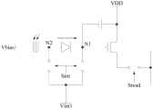
图4为依据本发明一实施例的超声波像素电路400的功能方框图。超声波像素电路400包含峰值检测元件DI、复位电路410、以及输出电路420。峰值检测元件DI耦接于第一节点N1和第二节点N2之间,且通过第二节点N2耦接于超声波传感器PM的一端。超声波传感器PM的另一端用于接收驱动电压Vbias,驱动电压Vbias用于利用振荡(oscillation)波形来驱动超声波传感器PM发射超声波。FIG. 4 is a functional block diagram of an
峰值检测元件DI用于将超声波传感器PM于第二节点N2产生的电压振荡转换为对应的电荷并储存于第一节点N1。实际上,峰值检测元件DI可以用PN二极管元件或是PIN二极管元件来实现,其中二极管元件的阳极端和阴极端分别耦接于第二节点N2和第一节点N1。The peak detection element DI is used for converting the voltage oscillation generated by the ultrasonic sensor PM at the second node N2 into corresponding charges and storing them at the first node N1. In fact, the peak detection element DI can be realized by a PN diode element or a PIN diode element, wherein the anode end and the cathode end of the diode element are respectively coupled to the second node N2 and the first node N1 .
复位电路410耦接于第一节点N1和第二节点N2,用于设置第一节点N1和第二节点N2的电压,且包含第一开关T1和第二开关T2。第一开关T1的第一端耦接于第一节点N1。第二开关T2的第一端耦接于第二节点N2。第一开关T1的第二端和第二开关T2的第二端用于接收第一参考电压Vint1。第一开关T1的控制端和第二开关T2的控制端用于接收复位控制信号Sint,亦即当复位电路410设置第一节点N1的电压时,复位电路410也会设置第二节点N2的电压。The
输出电路420耦接于第一节点N1,用于依据第一节点N1的电压提供感测电流Ise,且包含驱动晶体管Tr、输出开关To、以及储存电容Cst。驱动晶体管Tr的第一端用于接收系统电压VDD,驱动晶体管Tr的控制端则耦接于第一节点N1。输出开关To的第一端耦接于驱动晶体管Tr的第二端,输出开关To的第二端耦接于感测数据线Lse,输出开关To的控制端用于接收输出控制信号Sread。储存电容Cst的第一端耦接于第一节点N1,储存电容Cst的第二端则用于接收系统电压VDD。The
在本实施例中,储存电容Cst为驱动晶体管Tr的第一端(例如,源极)和控制端(例如,栅极)之间的寄生电容元件,但本发明并不以此为限。在一实施例中,储存电容Cst和驱动晶体管Tr为不同的元件。例如,储存电容Cst可以是利用不同金属层重叠而形成的电容元件。In this embodiment, the storage capacitor Cst is a parasitic capacitance element between the first terminal (eg, source) and the control terminal (eg, gate) of the driving transistor Tr, but the invention is not limited thereto. In one embodiment, the storage capacitor Cst and the driving transistor Tr are different components. For example, the storage capacitor Cst may be a capacitive element formed by overlapping different metal layers.
实际上,图4的第一开关T1、第二开关T2、驱动晶体管Tr、以及输出开关To可以用各种合适种类的P型晶体管来实现。例如,P型薄膜晶体管或P型金氧半场效晶体管。Actually, the first switch T1 , the second switch T2 , the driving transistor Tr, and the output switch To in FIG. 4 can be realized by various suitable types of P-type transistors. For example, a P-type thin film transistor or a P-type metal oxide semiconductor field effect transistor.
在一实施例中,图4的超声波像素电路400和超声波传感器PM,分别可用于实现图3的超声波像素电路312和超声波传感器PM。在此情况下,感测数据线Lse是耦接于图3中的一行超声波像素电路312和对应的一个电流检测电路324。超声波像素电路400(亦即,超声波像素电路312)可将感测电流Ise作为感测结果,通过感测数据线Lse输出至电流检测电路324。In one embodiment, the
图5为图4的超声波像素电路400的多个控制信号与节点电压的波形示意图。图6A至6C为图4的超声波像素电路400在不同运作阶段中的等效电路操作示意图。FIG. 5 is a schematic diagram of waveforms of multiple control signals and node voltages of the
请参照图5和图6A,在复位阶段P1中,复位控制信号Sint具有逻辑高电位(例如,低电压电位),输出控制信号Sread具有逻辑低电位(例如,高电压电位),且驱动电压Vbias具有振荡波形。因此,第一开关T1和第二开关T2会导通,以将第一节点N1和第二节点N2的电压维持于第一参考电压Vint1,进而关断峰值检测元件DI。输出开关To会关断,且超声波传感器PM会产生超声波。5 and 6A, in the reset phase P1, the reset control signal Sint has a logic high potential (for example, a low voltage potential), the output control signal Sread has a logic low potential (for example, a high voltage potential), and the driving voltage Vbias Has an oscillating waveform. Therefore, the first switch T1 and the second switch T2 are turned on to maintain the voltages of the first node N1 and the second node N2 at the first reference voltage Vint1 , and then turn off the peak detection element DI. The output switch To will be turned off, and the ultrasonic sensor PM will generate ultrasonic waves.
请参照图5和图6B,在感测阶段P2中,复位控制信号Sint和输出控制信号Sread都具有逻辑低电位,且驱动电压Vbias维持于固定电位。因此,第一开关T1、第二开关T2、以及输出开关To会关断。当超声波传感器PM接收到反射的超声波而震动时,第二节点N2的电压会具有对应的振荡波形。若第二节点N2的电压高于一预设电位Vp,峰值检测元件DI会导通而将第二节点N2的电荷传递至第一节点N1。Referring to FIG. 5 and FIG. 6B , in the sensing phase P2 , both the reset control signal Sint and the output control signal Sread have a logic low level, and the driving voltage Vbias is maintained at a fixed level. Therefore, the first switch T1, the second switch T2, and the output switch To are turned off. When the ultrasonic sensor PM receives the reflected ultrasonic wave and vibrates, the voltage of the second node N2 will have a corresponding oscillation waveform. If the voltage of the second node N2 is higher than a predetermined potential Vp, the peak detection element DI is turned on to transmit the charge of the second node N2 to the first node N1.
换言之,第一节点N1在感测阶段P2中所获得的电荷量,会对应于超声波传感器PM的震动强度和频率等等因素。In other words, the charge amount obtained by the first node N1 in the sensing phase P2 will correspond to factors such as the vibration intensity and frequency of the ultrasonic sensor PM.
请参照图5和图6C,在输出阶段P3中,复位控制信号Sint具有逻辑低电位,输出控制信号Sread具有逻辑高电位,且驱动电压Vbias维持于固定电位。因此,第一开关T1和第二开关T2会关断,而输出开关To会导通。由于驱动晶体管Tr工作于饱和区,驱动晶体管Tr会提供感测电流Ise,且感测电流Ise的大小会对应于第一节点N1的电压。感测电流Ise会经由输出开关To输出至感测数据线Lse。Referring to FIG. 5 and FIG. 6C, in the output phase P3, the reset control signal Sint has a logic low level, the output control signal Sread has a logic high level, and the driving voltage Vbias is maintained at a fixed level. Therefore, the first switch T1 and the second switch T2 are turned off, and the output switch To is turned on. Since the driving transistor Tr works in the saturation region, the driving transistor Tr provides the sensing current Ise, and the magnitude of the sensing current Ise corresponds to the voltage of the first node N1. The sensing current Ise is output to the sensing data line Lse through the output switch To.
图7为依据本发明一实施例的超声波像素电路700的功能方框图。图7的超声波像素电路700类似于图4的超声波像素电路400,差异在于,超声波像素电路700的峰值检测元件DI的耦接方向相反于超声波像素电路400的峰值检测元件DI。例如,在超声波像素电路700的峰值检测元件DI是以二极管来实现的一实施例中,超声波像素电路700的峰值检测元件DI是以阳极端耦接于第一节点N1,并以阴极端耦接于第二节点N2。FIG. 7 is a functional block diagram of an
于感测阶段P2中,若第二节点N2的电压低于另一预设电位,超声波像素电路700的峰值检测元件DI会导通,进而将第一节点N1的电荷传递至第二节点N2。In the sensing phase P2, if the voltage of the second node N2 is lower than another predetermined potential, the peak detection element DI of the
图8为依据本发明一实施例的超声波像素电路800的功能方框图。图8的超声波像素电路800类似于图4的超声波像素电路400,差异在于,超声波像素电路800的第一开关T1的第二端耦接于第二节点N2(亦即,第二开关T2的第一端)。FIG. 8 is a functional block diagram of an
图9为依据本发明一实施例的超声波像素电路900的功能方框图。图9的超声波像素电路900类似于图4的超声波像素电路400,差异在于,超声波像素电路900的第二开关T2的第二端耦接于第一节点N1(亦即,第一开关T1的第一端)。FIG. 9 is a functional block diagram of an
图10为依据本发明一实施例的超声波像素电路1000的功能方框图。图10的超声波像素电路1000类似于图4的超声波像素电路400,差异在于,超声波像素电路1000的第一开关T1的第二端用于接收第一参考电压Vint1,超声波像素电路1000的第二开关T2的第二端用于接收第二参考电压Vint2,且第一参考电压Vint1不同于第二参考电压Vint2。在一实施例中,第一参考电压Vint1低于第二参考电压Vint2。FIG. 10 is a functional block diagram of an
由上述可知,上述的多个实施例中的显示装置和超声波像素电路具有精简的电路架构,因而能达成高解析度的指纹、手势、或触控侦测,并降低制造复杂度。From the above, it can be seen that the display device and the ultrasonic pixel circuit in the above-mentioned embodiments have a simplified circuit structure, so that high-resolution fingerprint, gesture, or touch detection can be achieved, and manufacturing complexity can be reduced.
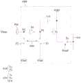
图11为图4的超声波像素电路400在一实施例中的模拟示意图。图12为图4的超声波像素电路400在另一实施例中的模拟示意图。由图11可知,在感测阶段P2中,当第二节点N2的电压具有峰值约为2.5V的振荡波形时,第一节点N1的电压会由0V上升至约1.7V。由图12可知,在感测阶段P2中,当第二节点N2的电压具有峰值约为3.0V的振荡波形时,第一节点N1的电压会由0V上升至约2.2V。FIG. 11 is a schematic diagram of a simulation of the
因此,在系统电压VDD被设置为约4~6V且感测数据线Lse的电压被合理地设置为约1.4V的情况下,驱动晶体管Tr便可以工作于饱和区,进而输出对应于第一节点N1的电压的驱动电流Ise。Therefore, when the system voltage VDD is set to about 4-6V and the voltage of the sensing data line Lse is reasonably set to about 1.4V, the driving transistor Tr can work in the saturation region, and the output corresponding to the first node The driving current Ise of the voltage of N1.
在上述的多个实施例中,系统电压VDD高于感测数据线Lse的电压,但本发明不以此为限。在某些实施例中,图4、7~10的系统电压VDD低于感测数据线Lse的电压,使得驱动晶体管Tr在输出阶段P3中会自感测数据线Lse抽取感测电流Ise。In the above-mentioned multiple embodiments, the system voltage VDD is higher than the voltage of the sensing data line Lse, but the present invention is not limited thereto. In some embodiments, the system voltage VDD in FIGS. 4, 7-10 is lower than the voltage of the sensing data line Lse, so that the driving transistor Tr draws the sensing current Ise from the sensing data line Lse in the output phase P3.
在另外一些实施例中,图4、7~10的第一开关T1和第二开关T2可以用N型晶体管来实现,且复位控制信号Sint会对应地具有与图5反相的波形。另外,输出开关To也可以用N型晶体管来实现,且输出控制信号Sread会对应地具有与图5反相的波形。In some other embodiments, the first switch T1 and the second switch T2 in FIGS. 4 , 7-10 can be implemented by N-type transistors, and the reset control signal Sint will have a waveform opposite to that in FIG. 5 . In addition, the output switch To can also be implemented with an N-type transistor, and the output control signal Sread will correspondingly have a waveform opposite to that shown in FIG. 5 .
在说明书及权利要求书中使用了某些词汇来指称特定的元件。然而,所属技术领域中具有通常知识者应可理解,同样的元件可能会用不同的名词来称呼。说明书及权利要求书并不以名称的差异做为区分元件的方式,而是以元件在功能上的差异来做为区分的基准。在说明书及权利要求书所提及的「包含」为开放式的用语,故应解释成「包含但不限定于」。另外,「耦接」在此包含任何直接及间接的连接手段。因此,若文中描述第一元件耦接于第二元件,则代表第一元件可通过电性连接或无线传输、光学传输等信号连接方式而直接地连接于第二元件,或者通过其他元件或连接手段间接地电性或信号连接至该第二元件。Certain terms are used in the description and claims to refer to particular elements. However, those skilled in the art should understand that the same element may be called by different terms. The specification and claims do not use the difference in name as a way to distinguish components, but use the difference in function of components as a basis for distinction. The "comprising" mentioned in the specification and claims is an open term, so it should be interpreted as "including but not limited to". In addition, "coupling" here includes any direct and indirect connection means. Therefore, if it is described that the first element is coupled to the second element, it means that the first element can be directly connected to the second element through electrical connection or signal connection means such as wireless transmission or optical transmission, or through other elements or connections. The means are indirectly electrically or signally connected to the second element.
在此所使用的「及/或」的描述方式,包含所列举的其中之一或多个项目的任意组合。另外,除非说明书中特别指明,否则任何单数的用语都同时包含复数的涵义。The description of "and/or" used herein includes any combination of one or more of the listed items. In addition, unless otherwise specified in the specification, any singular terms also include plural meanings.
当然,本发明还可有其它多种实施例,在不背离本发明精神及其实质的情况下,熟悉本领域的技术人员当可根据本发明作出各种相应的改变和变形,但这些相应的改变和变形都应属于本发明所附的权利要求的保护范围。Certainly, the present invention also can have other multiple embodiments, without departing from the spirit and essence of the present invention, those skilled in the art can make various corresponding changes and deformations according to the present invention, but these corresponding Changes and deformations should belong to the scope of protection of the appended claims of the present invention.
Claims (10)
Applications Claiming Priority (2)
| Application Number | Priority Date | Filing Date | Title |
|---|---|---|---|
| TW108125307 | 2019-07-17 | ||
| TW108125307ATWI701585B (en) | 2019-07-17 | 2019-07-17 | Ultrasonic pixel circuit and related display device |
Publications (2)
| Publication Number | Publication Date |
|---|---|
| CN111126352A CN111126352A (en) | 2020-05-08 |
| CN111126352Btrue CN111126352B (en) | 2023-06-13 |
Family
ID=70492733
Family Applications (1)
| Application Number | Title | Priority Date | Filing Date |
|---|---|---|---|
| CN202010071365.9AActiveCN111126352B (en) | 2019-07-17 | 2020-01-21 | Ultrasonic pixel circuit and related display device |
Country Status (2)
| Country | Link |
|---|---|
| CN (1) | CN111126352B (en) |
| TW (1) | TWI701585B (en) |
Families Citing this family (2)
| Publication number | Priority date | Publication date | Assignee | Title |
|---|---|---|---|---|
| TWI750011B (en)* | 2021-01-19 | 2021-12-11 | 友達光電股份有限公司 | Ultrasonic driving circuit |
| CN112883828B (en)* | 2021-01-28 | 2022-08-16 | 厦门天马微电子有限公司 | Ultrasonic fingerprint identification circuit, display panel, display device and driving method |
Citations (5)
| Publication number | Priority date | Publication date | Assignee | Title |
|---|---|---|---|---|
| CN105378617A (en)* | 2013-07-15 | 2016-03-02 | 高通股份有限公司 | Method and integrated circuit for operating sensor array |
| CN105393261A (en)* | 2013-06-03 | 2016-03-09 | 高通股份有限公司 | Display with peripherally configured ultrasonic biometric sensor |
| CN108351403A (en)* | 2016-03-03 | 2018-07-31 | 密克罗奇普技术公司 | Ultrasonic wave proximity sensing peripheral equipment based on core independence peripheral equipment |
| CN109598258A (en)* | 2018-12-30 | 2019-04-09 | 苏州迈瑞微电子有限公司 | Ultrasound detection circuit and image sensor pixel circuit and signal detecting method |
| CN110008897A (en)* | 2019-04-02 | 2019-07-12 | 京东方科技集团股份有限公司 | Ultrasonic sensor pixel circuit and driving method thereof, and display panel |
Family Cites Families (4)
| Publication number | Priority date | Publication date | Assignee | Title |
|---|---|---|---|---|
| US8890853B2 (en)* | 2013-01-11 | 2014-11-18 | Sharp Laboratories Of America, Inc. | In-pixel ultrasonic touch sensor for display applications |
| US10497748B2 (en)* | 2015-10-14 | 2019-12-03 | Qualcomm Incorporated | Integrated piezoelectric micromechanical ultrasonic transducer pixel and array |
| US20180373913A1 (en)* | 2017-06-26 | 2018-12-27 | Qualcomm Incorporated | Ultrasonic fingerprint sensor for under-display applications |
| US10775500B2 (en)* | 2017-09-14 | 2020-09-15 | Qualcomm Incorporated | Ultrasonic transducer pixel readout circuitry and methods for ultrasonic phase imaging |
- 2019
- 2019-07-17TWTW108125307Apatent/TWI701585B/enactive
- 2020
- 2020-01-21CNCN202010071365.9Apatent/CN111126352B/enactiveActive
Patent Citations (5)
| Publication number | Priority date | Publication date | Assignee | Title |
|---|---|---|---|---|
| CN105393261A (en)* | 2013-06-03 | 2016-03-09 | 高通股份有限公司 | Display with peripherally configured ultrasonic biometric sensor |
| CN105378617A (en)* | 2013-07-15 | 2016-03-02 | 高通股份有限公司 | Method and integrated circuit for operating sensor array |
| CN108351403A (en)* | 2016-03-03 | 2018-07-31 | 密克罗奇普技术公司 | Ultrasonic wave proximity sensing peripheral equipment based on core independence peripheral equipment |
| CN109598258A (en)* | 2018-12-30 | 2019-04-09 | 苏州迈瑞微电子有限公司 | Ultrasound detection circuit and image sensor pixel circuit and signal detecting method |
| CN110008897A (en)* | 2019-04-02 | 2019-07-12 | 京东方科技集团股份有限公司 | Ultrasonic sensor pixel circuit and driving method thereof, and display panel |
Also Published As
| Publication number | Publication date |
|---|---|
| TW202105152A (en) | 2021-02-01 |
| CN111126352A (en) | 2020-05-08 |
| TWI701585B (en) | 2020-08-11 |
Similar Documents
| Publication | Publication Date | Title |
|---|---|---|
| US10691911B2 (en) | Array substrate, display panel, display device and method for manufacturing array substrate | |
| US10614282B2 (en) | Pressure sensing assembly integrated with fingerprint identification function, driving method thereof, and display device | |
| CN103871378B (en) | Driving circuit for providing touch function by display structure and touch display | |
| TWI428661B (en) | Touch display apparatus | |
| EP3637304A1 (en) | Fingerprint identification substrate, fingerprint identification method, and display device | |
| CN108509829B (en) | Display base plate and its driving method, display device | |
| CN110245636A (en) | A kind of fingerprint recognition mould group, display panel, display device and fingerprint identification method | |
| US20080018612A1 (en) | Display device | |
| CN108229395B (en) | Fingerprint recognition detection circuit and touch panel | |
| CN107195264A (en) | Photo-detector and its driving method, display panel and display device | |
| US8658957B2 (en) | Sensor circuit and display apparatus | |
| CN112215215B (en) | Electronic Devices | |
| CN110110691A (en) | Fingerprint recognition driving circuit, module, touch screen and driving method | |
| CN101349821A (en) | Reading circuit for obtaining light intensity and electronic system | |
| EP3816847B1 (en) | Ultrasonic signal detecting circuit and ultrasonic signal detecting method | |
| CN109298804B (en) | Touch circuit and driving method thereof, touch substrate and display device | |
| CN112117303B (en) | Display panels and display devices | |
| CN111126352B (en) | Ultrasonic pixel circuit and related display device | |
| CN110110659A (en) | Array substrate and display device | |
| US20220165079A1 (en) | Electronic apparatus having fingerprint sensing function | |
| CN108171192A (en) | Fingerprint recognition detection circuit and its driving method, display device | |
| CN101900904B (en) | Flat display and touch panel with touch function | |
| CN110135348B (en) | Fingerprint detection circuit, driving method thereof, array substrate and display device | |
| CN111857405B (en) | Touch display panel and touch control circuit | |
| US11900718B2 (en) | Method of operating a sensing circuit to reduce effect of parasitic capacitors between sensing wires of the sensing circuit |
Legal Events
| Date | Code | Title | Description |
|---|---|---|---|
| PB01 | Publication | ||
| PB01 | Publication | ||
| SE01 | Entry into force of request for substantive examination | ||
| SE01 | Entry into force of request for substantive examination | ||
| GR01 | Patent grant | ||
| GR01 | Patent grant |