CN111081738A - OLED display panel - Google Patents
OLED display panelDownload PDFInfo
- Publication number
- CN111081738A CN111081738ACN201911238605.3ACN201911238605ACN111081738ACN 111081738 ACN111081738 ACN 111081738ACN 201911238605 ACN201911238605 ACN 201911238605ACN 111081738 ACN111081738 ACN 111081738A
- Authority
- CN
- China
- Prior art keywords
- display panel
- layer
- pixel definition
- display area
- definition layer
- Prior art date
- Legal status (The legal status is an assumption and is not a legal conclusion. Google has not performed a legal analysis and makes no representation as to the accuracy of the status listed.)
- Granted
Links
Images


Classifications
- H—ELECTRICITY
- H10—SEMICONDUCTOR DEVICES; ELECTRIC SOLID-STATE DEVICES NOT OTHERWISE PROVIDED FOR
- H10K—ORGANIC ELECTRIC SOLID-STATE DEVICES
- H10K59/00—Integrated devices, or assemblies of multiple devices, comprising at least one organic light-emitting element covered by group H10K50/00
- H10K59/10—OLED displays
- H10K59/12—Active-matrix OLED [AMOLED] displays
- H10K59/121—Active-matrix OLED [AMOLED] displays characterised by the geometry or disposition of pixel elements
- H10K59/1213—Active-matrix OLED [AMOLED] displays characterised by the geometry or disposition of pixel elements the pixel elements being TFTs
- H—ELECTRICITY
- H05—ELECTRIC TECHNIQUES NOT OTHERWISE PROVIDED FOR
- H05K—PRINTED CIRCUITS; CASINGS OR CONSTRUCTIONAL DETAILS OF ELECTRIC APPARATUS; MANUFACTURE OF ASSEMBLAGES OF ELECTRICAL COMPONENTS
- H05K3/00—Apparatus or processes for manufacturing printed circuits
- H05K3/30—Assembling printed circuits with electric components, e.g. with resistor
- H05K3/32—Assembling printed circuits with electric components, e.g. with resistor electrically connecting electric components or wires to printed circuits
- H05K3/321—Assembling printed circuits with electric components, e.g. with resistor electrically connecting electric components or wires to printed circuits by conductive adhesives
- H05K3/323—Assembling printed circuits with electric components, e.g. with resistor electrically connecting electric components or wires to printed circuits by conductive adhesives by applying an anisotropic conductive adhesive layer over an array of pads
- H—ELECTRICITY
- H10—SEMICONDUCTOR DEVICES; ELECTRIC SOLID-STATE DEVICES NOT OTHERWISE PROVIDED FOR
- H10K—ORGANIC ELECTRIC SOLID-STATE DEVICES
- H10K59/00—Integrated devices, or assemblies of multiple devices, comprising at least one organic light-emitting element covered by group H10K50/00
- H10K59/10—OLED displays
- H10K59/12—Active-matrix OLED [AMOLED] displays
- H10K59/1201—Manufacture or treatment
- H—ELECTRICITY
- H10—SEMICONDUCTOR DEVICES; ELECTRIC SOLID-STATE DEVICES NOT OTHERWISE PROVIDED FOR
- H10K—ORGANIC ELECTRIC SOLID-STATE DEVICES
- H10K59/00—Integrated devices, or assemblies of multiple devices, comprising at least one organic light-emitting element covered by group H10K50/00
- H10K59/10—OLED displays
- H10K59/12—Active-matrix OLED [AMOLED] displays
- H10K59/123—Connection of the pixel electrodes to the thin film transistors [TFT]
- H—ELECTRICITY
- H10—SEMICONDUCTOR DEVICES; ELECTRIC SOLID-STATE DEVICES NOT OTHERWISE PROVIDED FOR
- H10K—ORGANIC ELECTRIC SOLID-STATE DEVICES
- H10K59/00—Integrated devices, or assemblies of multiple devices, comprising at least one organic light-emitting element covered by group H10K50/00
- H10K59/10—OLED displays
- H10K59/12—Active-matrix OLED [AMOLED] displays
- H10K59/126—Shielding, e.g. light-blocking means over the TFTs
- H—ELECTRICITY
- H10—SEMICONDUCTOR DEVICES; ELECTRIC SOLID-STATE DEVICES NOT OTHERWISE PROVIDED FOR
- H10K—ORGANIC ELECTRIC SOLID-STATE DEVICES
- H10K59/00—Integrated devices, or assemblies of multiple devices, comprising at least one organic light-emitting element covered by group H10K50/00
- H10K59/10—OLED displays
- H10K59/12—Active-matrix OLED [AMOLED] displays
- H10K59/131—Interconnections, e.g. wiring lines or terminals
- H—ELECTRICITY
- H10—SEMICONDUCTOR DEVICES; ELECTRIC SOLID-STATE DEVICES NOT OTHERWISE PROVIDED FOR
- H10K—ORGANIC ELECTRIC SOLID-STATE DEVICES
- H10K71/00—Manufacture or treatment specially adapted for the organic devices covered by this subclass
- H10K71/80—Manufacture or treatment specially adapted for the organic devices covered by this subclass using temporary substrates
- H—ELECTRICITY
- H05—ELECTRIC TECHNIQUES NOT OTHERWISE PROVIDED FOR
- H05K—PRINTED CIRCUITS; CASINGS OR CONSTRUCTIONAL DETAILS OF ELECTRIC APPARATUS; MANUFACTURE OF ASSEMBLAGES OF ELECTRICAL COMPONENTS
- H05K1/00—Printed circuits
- H05K1/18—Printed circuits structurally associated with non-printed electric components
- H05K1/189—Printed circuits structurally associated with non-printed electric components characterised by the use of a flexible or folded printed circuit
- H—ELECTRICITY
- H05—ELECTRIC TECHNIQUES NOT OTHERWISE PROVIDED FOR
- H05K—PRINTED CIRCUITS; CASINGS OR CONSTRUCTIONAL DETAILS OF ELECTRIC APPARATUS; MANUFACTURE OF ASSEMBLAGES OF ELECTRICAL COMPONENTS
- H05K2201/00—Indexing scheme relating to printed circuits covered by H05K1/00
- H05K2201/10—Details of components or other objects attached to or integrated in a printed circuit board
- H05K2201/10007—Types of components
- H05K2201/10128—Display
- H—ELECTRICITY
- H10—SEMICONDUCTOR DEVICES; ELECTRIC SOLID-STATE DEVICES NOT OTHERWISE PROVIDED FOR
- H10K—ORGANIC ELECTRIC SOLID-STATE DEVICES
- H10K2102/00—Constructional details relating to the organic devices covered by this subclass
- H10K2102/301—Details of OLEDs
- H10K2102/311—Flexible OLED
- H—ELECTRICITY
- H10—SEMICONDUCTOR DEVICES; ELECTRIC SOLID-STATE DEVICES NOT OTHERWISE PROVIDED FOR
- H10K—ORGANIC ELECTRIC SOLID-STATE DEVICES
- H10K59/00—Integrated devices, or assemblies of multiple devices, comprising at least one organic light-emitting element covered by group H10K50/00
- H10K59/10—OLED displays
- H10K59/12—Active-matrix OLED [AMOLED] displays
- H10K59/122—Pixel-defining structures or layers, e.g. banks
- H—ELECTRICITY
- H10—SEMICONDUCTOR DEVICES; ELECTRIC SOLID-STATE DEVICES NOT OTHERWISE PROVIDED FOR
- H10K—ORGANIC ELECTRIC SOLID-STATE DEVICES
- H10K59/00—Integrated devices, or assemblies of multiple devices, comprising at least one organic light-emitting element covered by group H10K50/00
- H10K59/10—OLED displays
- H10K59/12—Active-matrix OLED [AMOLED] displays
- H10K59/124—Insulating layers formed between TFT elements and OLED elements
- H—ELECTRICITY
- H10—SEMICONDUCTOR DEVICES; ELECTRIC SOLID-STATE DEVICES NOT OTHERWISE PROVIDED FOR
- H10K—ORGANIC ELECTRIC SOLID-STATE DEVICES
- H10K71/00—Manufacture or treatment specially adapted for the organic devices covered by this subclass
- H—ELECTRICITY
- H10—SEMICONDUCTOR DEVICES; ELECTRIC SOLID-STATE DEVICES NOT OTHERWISE PROVIDED FOR
- H10K—ORGANIC ELECTRIC SOLID-STATE DEVICES
- H10K77/00—Constructional details of devices covered by this subclass and not covered by groups H10K10/80, H10K30/80, H10K50/80 or H10K59/80
- H10K77/10—Substrates, e.g. flexible substrates
- H10K77/111—Flexible substrates
Landscapes
- Engineering & Computer Science (AREA)
- Microelectronics & Electronic Packaging (AREA)
- Manufacturing & Machinery (AREA)
- Physics & Mathematics (AREA)
- Geometry (AREA)
- Electroluminescent Light Sources (AREA)
- Devices For Indicating Variable Information By Combining Individual Elements (AREA)
Abstract
Translated fromChinese
Description
Translated fromChinese技术领域technical field
本申请涉及显示领域,特别是涉及一种OLED显示面板。The present application relates to the field of display, and in particular, to an OLED display panel.
背景技术Background technique
现有的OLED显示面板由于其低功耗、可弯曲的特性对可穿戴式设备的应用带来深远的影响,未来柔性屏幕将随着个人智能终端的不断渗透而广泛应用。但在OLED显示面板的生产过程中,设置在所述显示面板与所述显示面板上的柔性印制电路板之间的异方性导电胶(ACF,Anisotropic Conductive Film)受热融化,会溢出所述显示面板,流到所述显示面板的边缘,进而粘连所述显示面板的聚酰亚胺柔性层和衬底基板,使得后续使用激光剥离所述聚酰亚胺柔性层和所述衬底基板时的难度增加,甚至无法分开。The existing OLED display panel has a profound impact on the application of wearable devices due to its low power consumption and bendable characteristics. In the future, flexible screens will be widely used with the continuous penetration of personal smart terminals. However, during the production process of the OLED display panel, the anisotropic conductive film (ACF, Anisotropic Conductive Film) disposed between the display panel and the flexible printed circuit board on the display panel is heated and melted, which will overflow the The display panel flows to the edge of the display panel, and then adheres the polyimide flexible layer and the base substrate of the display panel, so that when the polyimide flexible layer and the base substrate are subsequently peeled off by laser The difficulty increases, and even cannot be separated.
因此,现有的OLED显示面板技术中,还存在着OLED显示面板的制作过程中,OLED显示面板内由于缺少能够阻挡异方性导电胶溢出显示面板显示区的结构,使得所述显示面板内的聚酰亚胺柔性层和衬底基板容易粘连在一起难以分开,影响后续的生产工艺以及显示面板的显示质量的问题,急需改进。Therefore, in the existing OLED display panel technology, there is still a manufacturing process of the OLED display panel. Due to the lack of a structure in the OLED display panel that can prevent the anisotropic conductive adhesive from overflowing the display area of the display panel, the The polyimide flexible layer and the base substrate are easy to stick together and difficult to separate, which affects the subsequent production process and the display quality of the display panel, and needs to be improved urgently.
发明内容SUMMARY OF THE INVENTION
本申请涉及一种OLED显示面板,用于解决现有技术中存在着OLED显示面板的制作过程中,OLED显示面板内由于缺少能够阻挡异方性导电胶溢出显示面板显示区的结构,使得所述显示面板内的聚酰亚胺柔性层和衬底基板容易粘连在一起难以分开,影响后续的生产工艺以及显示面板的显示质量的问题。The present application relates to an OLED display panel, which is used to solve the problem that in the production process of the OLED display panel in the prior art, the OLED display panel lacks a structure that can prevent the anisotropic conductive adhesive from overflowing the display area of the display panel. The polyimide flexible layer and the base substrate in the display panel are easy to stick together and difficult to separate, which affects the subsequent production process and the display quality of the display panel.
为解决上述问题,本申请提供的技术方案如下:In order to solve the above-mentioned problems, the technical solutions provided by this application are as follows:
本申请提供的一种OLED显示面板,所述显示面板包括:显示区和非显示区;其中,The application provides an OLED display panel, the display panel includes: a display area and a non-display area; wherein,
所述显示区和所述非显示区均设置有多种不同的膜层结构;Both the display area and the non-display area are provided with a variety of different film layer structures;
所述非显示区内还设置有柔性印制电路板,以及粘接所述显示面板与所述柔性印制电路板的异方性导电胶;A flexible printed circuit board is also arranged in the non-display area, and anisotropic conductive adhesive for bonding the display panel and the flexible printed circuit board;
所述显示面板靠近所述非显示区的一侧,设置有一阻挡部,所述阻挡部覆盖一种或是多种不同的膜层,用于阻挡所述异方性导电胶从所述非显示区的边缘处溢出。One side of the display panel close to the non-display area is provided with a blocking portion, and the blocking portion covers one or more different film layers for blocking the anisotropic conductive adhesive from passing from the non-display area. overflow at the edge of the area.
根据本申请提供的一实施例,所述阻挡部包括:挡墙结构和沟槽。According to an embodiment provided by the present application, the blocking portion includes: a blocking wall structure and a groove.
根据本申请提供的一实施例,所述挡墙结构的厚度与所述沟槽的深度相等。According to an embodiment provided by the present application, the thickness of the retaining wall structure is equal to the depth of the groove.
根据本申请提供的一实施例,所述沟槽的形状为:矩形、“V”字形或是倒梯形;所述沟槽的形状为:矩形、三角形或是梯形。According to an embodiment provided in the present application, the shape of the groove is: rectangle, "V" shape or inverted trapezoid; the shape of the groove is: rectangle, triangle or trapezoid.
根据本申请提供的一实施例,所述多种不同膜层为:像素定义层、平坦层、间绝缘层、第一栅绝缘层、第二栅绝缘层、缓冲层以及聚酰亚胺柔性层中的一种或是多种的组合。According to an embodiment provided in the present application, the various film layers are: a pixel definition layer, a planarization layer, an inter-insulating layer, a first gate insulating layer, a second gate insulating layer, a buffer layer, and a polyimide flexible layer one or a combination of them.
根据本申请提供的一实施例,所述像素定义层分为:第一像素定义层、第二像素定义层和第三像素定义层;所述第二像素定义层设置在所述第一像素定义层和所述第三像素定义层之间,且所述第一像素定义层的厚度等于所述第三像素定义层的厚度,所述第二像素定义层的厚度小于所述第一像素定义层或是所述第三像素定义层的厚度。According to an embodiment provided in the present application, the pixel definition layer is divided into: a first pixel definition layer, a second pixel definition layer, and a third pixel definition layer; the second pixel definition layer is provided in the first pixel definition layer layer and the third pixel definition layer, and the thickness of the first pixel definition layer is equal to the thickness of the third pixel definition layer, and the thickness of the second pixel definition layer is smaller than the thickness of the first pixel definition layer Or the thickness of the third pixel definition layer.
根据本申请提供的一实施例,所述阻挡部的数量大于等于一个。According to an embodiment provided by the present application, the number of the blocking portions is greater than or equal to one.
根据本申请提供的一实施例,所述阻挡部的上端面与所述柔性印制电路板的下端面平齐。According to an embodiment provided in the present application, the upper end surface of the blocking portion is flush with the lower end surface of the flexible printed circuit board.
根据本申请提供的一实施例,所述显示面板包括:第一侧边、第二侧边、第三侧边和第四侧边;所述阻挡部平行于所述显示面板的所述第二侧边和所述第四侧边。According to an embodiment provided in the present application, the display panel includes: a first side, a second side, a third side and a fourth side; the blocking portion is parallel to the second side of the display panel side and the fourth side.
根据本申请提供的一实施例,所述柔性印制电路板背离所述显示面板的一侧还设置有驱动芯片。According to an embodiment provided in the present application, a driver chip is further disposed on the side of the flexible printed circuit board facing away from the display panel.
与现有技术相比,本申请提供的OLED显示面板的有益效果为:Compared with the prior art, the beneficial effects of the OLED display panel provided by the present application are:
1.本申请提供的OLED显示面板,通过在所述显示面板内设置有阻挡部,所述阻挡部覆盖多个不同的膜层,用于阻挡所述异方性导电胶从所述显示面板内溢出,减小后续的加工难度,避免对显示面板的显示质量造成影响;1. The OLED display panel provided by the present application is provided with a blocking part in the display panel, the blocking part covers a plurality of different film layers, and is used to block the anisotropic conductive adhesive from inside the display panel. overflow, reduce the difficulty of subsequent processing, and avoid affecting the display quality of the display panel;
2.所述阻挡部包括:沟槽和挡墙结构,所述沟槽和所述挡墙结构所覆盖的膜层数量相同,即所述沟槽的深度与所述挡墙结构的厚度相等,包含所述像素定义层在内的一种或是多种不同膜层的组合,提高所述显示面板与所述柔性印制电路板之间的粘连稳定性并有效地阻挡了所述异方性导电胶从所述非显示区的边缘处溢出对显示面板的显示质量的影响。2. The blocking part comprises: a groove and a retaining wall structure, the grooves and the retaining wall structure cover the same number of film layers, that is, the depth of the groove is equal to the thickness of the retaining wall structure, The combination of one or more different film layers including the pixel definition layer improves the adhesion stability between the display panel and the flexible printed circuit board and effectively blocks the anisotropy The influence of the conductive adhesive overflowing from the edge of the non-display area on the display quality of the display panel.
附图说明Description of drawings
为了更清楚地说明本申请实施例中的技术方案,下面将对实施例描述中所需要使用的附图作简单地介绍,显而易见地,下面描述中的附图仅仅是本申请的一些实施例,对于本领域技术人员来讲,在不付出创造性劳动的前提下,还可以根据这些附图获得其他的附图。In order to illustrate the technical solutions in the embodiments of the present application more clearly, the following briefly introduces the drawings that are used in the description of the embodiments. Obviously, the drawings in the following description are only some embodiments of the present application. For those skilled in the art, other drawings can also be obtained from these drawings without creative effort.
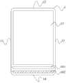
图1为本申请实施例提供的OLED显示面板的第一俯视结构示意图。FIG. 1 is a first top-view structural schematic diagram of an OLED display panel provided by an embodiment of the present application.
图2为本申请实施例提供的OLED显示面板的第二俯视结构示意图。FIG. 2 is a schematic diagram of a second top-view structure of the OLED display panel provided by the embodiment of the present application.
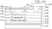
图3为本申请实施例提供的OLED显示面板的第一内部膜层结构图。FIG. 3 is a structural diagram of a first inner film layer of an OLED display panel provided by an embodiment of the present application.
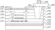
图4为本申请实施例提供的OLED显示面板的第二内部膜层结构图。FIG. 4 is a structural diagram of a second inner film layer of an OLED display panel provided by an embodiment of the present application.
图5为本申请实施例提供的OLED显示面板的第三内部膜层结构图。FIG. 5 is a structural diagram of a third inner film layer of an OLED display panel provided by an embodiment of the present application.
图6为本申请实施例提供的OLED显示面板的第四内部膜层结构图。FIG. 6 is a structural diagram of a fourth internal film layer of the OLED display panel provided by the embodiment of the present application.
图7为本申请实施例提供的OLED显示面板的第五内部膜层结构图。FIG. 7 is a structural diagram of a fifth inner film layer of the OLED display panel provided by the embodiment of the present application.
图8为本申请实施例提供的OLED显示面板的第六内部膜层结构图。FIG. 8 is a structural diagram of a sixth inner film layer of the OLED display panel provided by the embodiment of the present application.
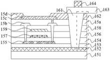
图9为本申请实施例提供的OLED显示面板的第七内部膜层结构图。FIG. 9 is a structural diagram of a seventh inner film layer of an OLED display panel provided by an embodiment of the present application.
图10为本申请实施例提供的OLED显示面板的第八内部膜层结构图。FIG. 10 is a structural diagram of an eighth internal film layer of the OLED display panel provided by the embodiment of the application.
具体实施方式Detailed ways
下面将结合本申请实施例中的附图,对本申请实施例中的技术方案进行清楚、完整地描述。显然,所描述的实施例仅仅是本申请一部分实施例,而不是全部的实施例。基于本申请中的实施例,本领域技术人员在没有作出创造性劳动前提下所获得的所有其他实施例,都属于本申请保护的范围。The technical solutions in the embodiments of the present application will be clearly and completely described below with reference to the accompanying drawings in the embodiments of the present application. Obviously, the described embodiments are only a part of the embodiments of the present application, but not all of the embodiments. Based on the embodiments in the present application, all other embodiments obtained by those skilled in the art without creative work fall within the protection scope of the present application.
在本申请的描述中,需要理解的是,术语“中心”、“纵向”、“横向”、“长度”、“宽度”、“厚度”、“上”、“下”、“前”、“后”、“左”、“右”、“竖直”、“水平”、“顶”、“底”、“内”、“外”、“顺时针”、“逆时针”等指示的方位或位置关系为基于附图所示的方位或位置关系,仅是为了便于描述本申请和简化描述,而不是指示或暗示所指的装置或元件必须具有特定的方位、以特定的方位构造和操作,因此不能理解为对本申请的限制。此外,术语“第一”、“第二”仅用于描述目的,而不能理解为指示或暗示相对重要性或者隐含指明所指示的技术特征的数量。由此,限定有“第一”、“第二”的特征可以明示或者隐含地包括一个或者更多个所述特征。在本申请的描述中,“多个”的含义是两个或两个以上,除非另有明确具体的限定。In the description of this application, it should be understood that the terms "center", "longitudinal", "lateral", "length", "width", "thickness", "upper", "lower", "front", " rear, left, right, vertical, horizontal, top, bottom, inside, outside, clockwise, counterclockwise, etc., or The positional relationship is based on the orientation or positional relationship shown in the accompanying drawings, which is only for the convenience of describing the present application and simplifying the description, rather than indicating or implying that the referred device or element must have a specific orientation, be constructed and operated in a specific orientation, Therefore, it should not be construed as a limitation on this application. In addition, the terms "first" and "second" are only used for descriptive purposes, and should not be construed as indicating or implying relative importance or implying the number of indicated technical features. Thus, features defined as "first", "second" may expressly or implicitly include one or more of said features. In the description of the present application, "plurality" means two or more, unless otherwise expressly and specifically defined.
在本申请的描述中,需要说明的是,除非另有明确的规定和限定,术语“安装”、“相连”、“连接”应做广义理解,例如,可以是固定连接,也可以是可拆卸连接,或一体地连接;可以是机械连接,也可以是电连接或可以相互通讯;可以是直接相连,也可以通过中间媒介间接相连,可以是两个元件内部的连通或两个元件的相互作用关系。对于本领域的普通技术人员而言,可以根据具体情况理解上述术语在本申请中的具体含义。In the description of this application, it should be noted that, unless otherwise expressly specified and limited, the terms "installed", "connected" and "connected" should be understood in a broad sense, for example, it may be a fixed connection or a detachable connection Connection, or integral connection; it can be mechanical connection, electrical connection or can communicate with each other; it can be directly connected or indirectly connected through an intermediate medium, it can be the internal communication of two elements or the interaction of two elements relation. For those of ordinary skill in the art, the specific meanings of the above terms in this application can be understood according to specific situations.
在本申请中,除非另有明确的规定和限定,第一特征在第二特征之“上”或之“下”可以包括第一和第二特征直接接触,也可以包括第一和第二特征不是直接接触而是通过它们之间的另外的特征接触。而且,第一特征在第二特征“之上”、“上方”和“上面”包括第一特征在第二特征正上方和斜上方,或仅仅表示第一特征水平高度高于第二特征。第一特征在第二特征“之下”、“下方”和“下面”包括第一特征在第二特征正下方和斜下方,或仅仅表示第一特征水平高度小于第二特征。In this application, unless otherwise expressly specified and defined, a first feature "on" or "under" a second feature may include direct contact between the first and second features, or may include the first and second features Not directly but through additional features between them. Also, the first feature being "above", "over" and "above" the second feature includes the first feature being directly above and obliquely above the second feature, or simply means that the first feature is level higher than the second feature. The first feature is "below", "below" and "below" the second feature includes the first feature being directly below and diagonally below the second feature, or simply means that the first feature has a lower level than the second feature.
下文的公开提供了许多不同的实施方式或例子用来实现本申请的不同结构。为了简化本申请的公开,下文中对特定例子的部件和设置进行描述。当然,它们仅仅为示例,并且目的不在于限制本申请。此外,本申请可以在不同例子中重复参考数字和/或参考字母,这种重复是为了简化和清楚的目的,其本身不指示所讨论各种实施方式和/或设置之间的关系。此外,本申请提供了的各种特定的工艺和材料的例子,但是本领域普通技术人员可以意识到其他工艺的应用和/或其他材料的使用。The following disclosure provides many different embodiments or examples for implementing different structures of the present application. To simplify the disclosure of the present application, the components and arrangements of specific examples are described below. Of course, they are only examples and are not intended to limit the application. Furthermore, this application may repeat reference numerals and/or reference letters in different instances for the purpose of simplicity and clarity, and does not in itself indicate a relationship between the various embodiments and/or arrangements discussed. In addition, this application provides examples of various specific processes and materials, but one of ordinary skill in the art will recognize the application of other processes and/or the use of other materials.
本申请提供一种OLED显示面板,具体参阅图1-图10。The present application provides an OLED display panel, please refer to FIG. 1 to FIG. 10 for details.
现有的显示面板,其所述显示面板与所述显示面板上的柔性印制电路板之间的异方性导电胶受热容易融化,其融化后会溢出所述显示面板,流到所述显示面板的边缘,进而粘连所述显示面板的聚酰亚胺柔性层和衬底基板,使得后续使用激光剥离所述聚酰亚胺柔性层和所述衬底基板时的难度增加,甚至无法分开。因此,为避免影响所述显示面板后续的生产工艺和显示质量,本申请提供一种OLED显示面板,在所述显示面板与所述柔性印制电路板接触的边缘处,设置沟槽和挡墙结构,以防止所述显示面板与所述柔性印制电路板之间的异方性导电胶从所述显示面板的边缘流出。In the existing display panel, the anisotropic conductive adhesive between the display panel and the flexible printed circuit board on the display panel is easily melted when heated, and after melting, it overflows the display panel and flows to the display panel. The edge of the panel is further adhered to the polyimide flexible layer of the display panel and the base substrate, which makes it more difficult to peel off the polyimide flexible layer and the base substrate using a laser subsequently, or even cannot be separated. Therefore, in order to avoid affecting the subsequent production process and display quality of the display panel, the present application provides an OLED display panel, in which grooves and retaining walls are arranged at the edge of the display panel in contact with the flexible printed circuit board. structure to prevent the anisotropic conductive adhesive between the display panel and the flexible printed circuit board from flowing out from the edge of the display panel.
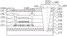
参阅图1,为本申请实施例提供的一种OLED显示面板的第一俯视图。所述显示面板1为矩形,包括四个侧边,即第一侧边11、第二侧边12、第三侧边13以及第四侧边14。所述显示面板上还设置有显示区15和非显示区16(图中未示出),所述显示区和所述非显示区均设置有多种不同的膜层结构;所述显示区15也为矩形,所述显示面板靠近所述非显示区16的一侧,设置有一阻挡部,即所述沟槽161和所述挡墙结构162。所述阻挡部覆盖一种或是多种不同的膜层,用于阻挡所述异方性导电胶(图中未示出)从所述非显示区的边缘处溢出。在本申请的一种实施例中,所述沟槽161和所述挡墙结构162的俯视图形状均为矩形,且平行于所述显示面板1的所述第二侧边12和所述第四侧边14。Referring to FIG. 1 , it is a first top view of an OLED display panel according to an embodiment of the present application. The display panel 1 is rectangular and includes four sides, namely a
参阅图2,为本申请实施例提供的一种OLED显示面板的第二俯视图。所述沟槽161和所述挡墙结构162的边缘均为与所述显示面板1的四个角相同的倒圆角结构,可以更好的保护所述显示面板内的异方性导电胶不从所述显示面板1的所述第四侧边14以及所述第四侧边14与所述第一侧边11以及所述第四侧边14与所述第三侧边13的夹角处溢出。Referring to FIG. 2 , it is a second top view of an OLED display panel according to an embodiment of the present application. The edges of the
参阅图3,为本申请实施例提供的一种OLED显示面板的第一内部膜层结构图。在本申请的一种实施例中,所述显示面板1的内部膜层包括:Referring to FIG. 3 , it is a structural diagram of a first inner film layer of an OLED display panel according to an embodiment of the present application. In an embodiment of the present application, the inner film layer of the display panel 1 includes:
基板151,所述基板151用于沉积各种膜层结构,所述基板151可以为刚性基板或是柔性基板,优选柔性基板;The
聚酰亚胺柔性层152,设置在所述基板151的一侧,采用聚酰亚胺涂布而成;The polyimide
缓冲层153,设置在所述聚酰亚胺柔性层152背离所述基板151的一侧,一般选用氮化硅作为材料;The
第一栅绝缘层154,设置在所述缓冲层153背离所述聚酰亚胺柔性层152的一侧;a first
半导体沟道层155,设置在所述第一栅绝缘层154内,靠近所述缓冲层的一侧,所述半导体沟道层155的两端一般需要进行离子掺杂;The
第二栅绝缘层156,设置在所述第一栅绝缘层154背离所述缓冲层153的一侧;The second
栅极层157,设置在所述第二栅绝缘层156内,靠近所述第一栅绝缘层154内,也作为显示驱动电容的下基板,用于给显示面板内的薄膜晶体管提供扫描信号;The
间绝缘层158,设置在所述第二栅绝缘层156背离所述第一栅绝缘层154的一侧,是一种用于阻隔所述源漏极层15b和所述显示驱动电容上基板159的无机层;The
显示驱动电容上基板159,设置在所述间绝缘层158内,靠近所述第二栅绝缘层156的一侧,与所述栅极层157一起形成显示驱动电路的电容;The display driving capacitor
平坦层15a,设置在所述间绝缘层158背离所述第二栅绝缘层156的一侧,使所述源漏极层15b的表面平坦化;The
源漏极层15b,设置在所述平坦层15a内部,通过所述间绝缘层158、所述第二栅绝缘层156以及所述第一栅绝缘层154与所述有源层155连通;The source-
阳极层15c,设置在所述平坦层15a背离所述间绝缘层158的一侧,与所述源漏极层15b电性连通;The
像素定义层15d,设置在所述平坦层15a背离所述间绝缘层158的一侧,并覆盖所述阳极层15c,用于限定有机发光材料的蒸镀区域且隔开R/G/B发光单元;The
柔性印制电路板163设置在所述显示面板1非显示区16靠近所述显示面板1的所述第四侧边14的边缘处,通过异方性导电胶(图中未示出)与所述显示面板1进行连接;The flexible printed
以及驱动芯片164,设置在所述柔性印制电路板163背离所述显示面板1的一侧。The
进一步地,所述沟槽161和所述挡墙结构162设置在所述显示面板1的非显示区靠近所述显示面板1的所述第四侧边14的一端;所述沟槽用于填塞所述异方性导电胶;所述挡墙结构162用于阻挡所述异方性导电胶溢出所述显示面板1,所述沟槽161的深度与所述挡墙结构162的厚度相同。在本申请的一种实施例中,所述沟槽161和所述挡墙结构162设置在所述像素定义层15d,即所述沟槽161的深度和所述挡墙结构162的厚度小于等于所述像素定义层15d的厚度。所述沟槽161的形状为倒梯形,所述挡墙结构162的形状为梯形。在本申请的其他实施例中,所述沟槽161的形状还可以是矩形或是“V”字形,所述挡墙结构162的形状还可以是矩形或是三角形,梯形还可以是等腰梯形、直角梯形或是不对称梯形,不限于附图4中所示的形状。当所述挡墙结构162的形状为梯形时,所述挡墙结构162覆盖的膜层数量越多,位于底层的膜层的宽度越大,位于上层的膜层宽度越小,膜层由上至下依次为:所述像素定义层15d、所述平坦层15a、所述间绝缘层158、所述第二栅绝缘层156、所述第一栅绝缘层154、所述柔性层153以及所述聚酰亚胺柔性层152;当所述挡墙结构162的形状为三角形时,膜层宽度的变化与所述挡墙结构162为梯形时的膜层变化相同;当所述挡墙结构162的形状为矩形时,位于底部的膜层的宽度和位于顶层的膜层的宽度相等。Further, the
在本申请的另一实施例中,所述沟槽161和所述挡墙结构162覆盖所述像素定义层15d和所述平坦层15a,即所述沟槽161的深度和所述挡墙结构162的厚度小于等于所述像素定义层15d与所述平坦层15a的厚度之和,参阅图4。In another embodiment of the present application, the
在本申请的其他实施例中,所述沟槽161和所述挡墙结构162可以是覆盖所述像素定义层15d、所述平坦层15a和所述间绝缘层158,即所述沟槽161的深度、所述挡墙结构162的厚度小于等于所述像素定义层15d、所述平坦层158和所述间绝缘层156之和,参阅图5;所述沟槽161的深度、所述挡墙结构162的厚度也可以是覆盖所述像素定义层15d、所述平坦层15a、所述间绝缘层158以及所述第二栅绝缘层156,即所述沟槽161的深度和所述挡墙结构162的厚度小于等于所述像素定义层15d、所述平坦层15a、所述间绝缘层158和所述第二栅绝缘层156之和,参阅图6;所述沟槽161的深度、所述挡墙结构162的厚度也可以是覆盖所述像素定义层15d、所述平坦层15a、所述间绝缘层158、所述第二栅绝缘层156以及所述第一栅绝缘层154,即所述沟槽161的深度和所述挡墙结构162的厚度小于等于所述像素定义层15d、所述平坦层15a、所述间绝缘层158、所述第二栅绝缘层156和所述第一栅绝缘层154之和,参阅图7;所述沟槽161的深度、所述挡墙结构162的厚度也可以是覆盖所述像素定义层15d、所述平坦层15a、所述间绝缘层158、所述第二栅绝缘层156、所述第一栅绝缘层154和所述缓冲层153,即所述沟槽161的深度、所述挡墙结构162的厚度小于等于所述像素定义层15d、所述平坦层15a、所述间绝缘层158、所述第二栅绝缘层156、所述第一栅绝缘层154和所述缓冲层153之和,参阅图8;所述沟槽161的深度、所述挡墙结构162的厚度还可以是覆盖所述像素定义层15d、所述平坦层15a、所述间绝缘层158、所述第二栅绝缘层156、所述第一栅绝缘层154、所述缓冲层153以及所述聚酰亚胺柔性层152,即所述沟槽161的深度、所述挡墙结构162的厚度小于等于所述像素定义层15d、所述平坦层15a、所述间绝缘层158、所述第二栅绝缘层156、所述第一栅绝缘层154、所述缓冲层153以及所述聚酰亚胺柔性层152之和,参阅图9。即所述沟槽161和所述挡墙结构162可以覆盖所述像素定义层15d、所述平坦层15a、所述间绝缘层158、所述第二栅绝缘层156、所述第一栅绝缘层154、所述缓冲层153以及所述聚酰亚胺柔性层152中的一种或是多种的组合。In other embodiments of the present application, the trench 161 and the retaining wall structure 162 may cover the pixel definition layer 15d, the flat layer 15a and the inter-insulating layer 158, that is, the trench 161 , the thickness of the retaining wall structure 162 is less than or equal to the sum of the pixel definition layer 15d, the flat layer 158 and the inter-insulating layer 156, see FIG. 5; the depth of the trench 161, the blocking The thickness of the wall structure 162 can also cover the pixel definition layer 15d, the flat layer 15a, the inter-insulating layer 158 and the second gate insulating layer 156, that is, the depth of the trench 161 and the barrier The thickness of the wall structure 162 is less than or equal to the sum of the pixel definition layer 15d, the flat layer 15a, the inter-insulating layer 158 and the second gate insulating layer 156, see FIG. 6; the depth of the trench 161, The thickness of the retaining wall structure 162 may also cover the pixel definition layer 15d, the flat layer 15a, the inter-insulating layer 158, the second gate insulating layer 156 and the first gate insulating layer 154, That is, the depth of the trench 161 and the thickness of the retaining wall structure 162 are less than or equal to the pixel definition layer 15d, the flat layer 15a, the inter-insulating layer 158, the second gate insulating layer 156 and the The sum of the first gate insulating layers 154, see FIG. 7; the depth of the trench 161 and the thickness of the retaining wall structure 162 may also cover the pixel definition layer 15d, the flat layer 15a, the inter-insulation layer Layer 158 , the second gate insulating layer 156 , the first gate insulating layer 154 and the buffer layer 153 , that is, the depth of the trench 161 and the thickness of the retaining wall structure 162 are less than or equal to the pixel definition The sum of the layer 15d, the flat layer 15a, the interlayer insulating layer 158, the second gate insulating layer 156, the first gate insulating layer 154 and the buffer layer 153, see FIG. 8; the trench The depth of 161 and the thickness of the retaining wall structure 162 may also cover the pixel definition layer 15d, the flat layer 15a, the inter-insulating layer 158, the second gate insulating layer 156, the first gate The insulating layer 154, the buffer layer 153 and the polyimide flexible layer 152, that is, the depth of the trench 161 and the thickness of the retaining wall structure 162 are less than or equal to the pixel definition layer 15d, the flat layer 15a, the sum of the inter-insulating layer 158 , the second gate insulating layer 156 , the first gate insulating layer 154 , the buffer layer 153 and the polyimide flexible layer 152 , see FIG. 9 . That is, the
进一步地,所述像素定义层15d分为:第一像素定义层15d1、第二像素定义层15d2和第三像素定义层15d3,且所述第一像素定义层15d1的厚度等于所述第三像素定义层15d3的厚度;在本申请的一种实施例中,所述第二像素定义层15d2的厚度略小于所述第一像素定义层15d1或是所述第三像素定义层15d3的厚度,以便于所述异方性导电胶流入所述沟槽161内,参阅图10。在另一种实施例中,所述第二像素定义层15d2的厚度等于所述第一像素定义层15d1或是所述第三像素定义层15d3的厚度。Further, the
进一步地,所述阻挡部的数量可以为一个或是多个,以增强对所述异方性导电胶的阻挡。所述阻挡部的上端面与所述柔性印制电路板163的下端面平齐,即当所述第二像素定义层15d2的厚度与所述第三像素定义层15d3的厚度相等时,所述阻挡部的上端面即为所述像素定义层15d的上端面,所述柔性印制电路板163的下端面与所述像素定义层15d的上端面平齐;当所述第二像素定义层15d2的厚度小于所述第三像素定义层15d3的厚度时,所述柔性印制电路板163的下端面与所述第三像素定义层15d3的上端面平齐。Further, the number of the blocking portion may be one or more, so as to enhance the blocking of the anisotropic conductive adhesive. The upper end surface of the blocking portion is flush with the lower end surface of the flexible printed
本申请还提供一种OLED显示面板的制作方法,包括下述步骤:The present application also provides a method for manufacturing an OLED display panel, comprising the following steps:
S10,提供一基板;S10, providing a substrate;
S20,在所述基板上依次沉积聚酰亚胺柔性层、缓冲层、第一栅绝缘层、半导体沟道层、第二栅绝缘层、栅极层、间绝缘层、显示驱动电容上基板、平坦层、源漏极层、阳极层以及像素定义层;S20, sequentially depositing a polyimide flexible layer, a buffer layer, a first gate insulating layer, a semiconductor channel layer, a second gate insulating layer, a gate layer, an inter-insulating layer, a display driving capacitor upper substrate, flat layer, source and drain layer, anode layer and pixel definition layer;
S30,采用精细化掩膜板在所述像素定义层背离所述阳极层的一侧进行图案化制程,再经曝光、显影去掉未被所述精细化掩膜板遮挡的部分,以制作成沟槽和挡墙结构;S30, using a fine mask to perform a patterning process on the side of the pixel definition layer away from the anode layer, and then exposing and developing to remove the part not covered by the fine mask to form grooves Slot and retaining wall structures;
S40,使用异方性导电胶将所述柔性印制电路板粘接在所述显示面板靠近所述非显示区的一端。S40, using anisotropic conductive adhesive to bond the flexible printed circuit board to one end of the display panel close to the non-display area.
进一步地,上述步骤“S20”中,所述源漏极层通过蚀刻与所述半导体沟道层电性连接,所述阳极层与所述源漏极层电性连接;上述步骤“S30”中所述的精细化掩膜板根据所述沟槽和所述挡墙结构形状的不同选用不同形状的精细化掩膜板进行制作。Further, in the above step "S20", the source and drain layers are electrically connected to the semiconductor channel layer by etching, and the anode layer is electrically connected to the source and drain layers; in the above step "S30" The refinement mask plate is made by selecting refinement mask plates of different shapes according to the different shapes of the trench and the retaining wall structure.
以上对本申请实施例所提供的一种OLED显示面板进行了详细介绍,本文中应用了具体个例对本申请的原理及实施方式进行了阐述,以上实施例的说明只是用于帮助理解本申请的技术方案及其核心思想;本领域的普通技术人员应当理解:其依然可以对前述各实施例所记载的技术方案进行修改,或者对其中部分技术特征进行等同替换;而这些修改或者替换,并不使相应技术方案的本质脱离本申请各实施例的技术方案的范围。An OLED display panel provided by the embodiments of the present application has been introduced in detail above. The principles and implementations of the present application are described with specific examples. The descriptions of the above embodiments are only used to help understand the technology of the present application. scheme and its core idea; those of ordinary skill in the art should understand that: it is still possible to modify the technical solutions recorded in the foregoing embodiments, or to perform equivalent replacements for some of the technical features; and these modifications or replacements do not make The essence of the corresponding technical solutions deviates from the scope of the technical solutions of the embodiments of the present application.
Claims (10)
Translated fromChinesePriority Applications (2)
| Application Number | Priority Date | Filing Date | Title |
|---|---|---|---|
| CN201911238605.3ACN111081738B (en) | 2019-12-06 | 2019-12-06 | OLED display panel |
| US16/812,880US20210175313A1 (en) | 2019-12-06 | 2020-03-09 | Organic light-emitting diode display panel |
Applications Claiming Priority (1)
| Application Number | Priority Date | Filing Date | Title |
|---|---|---|---|
| CN201911238605.3ACN111081738B (en) | 2019-12-06 | 2019-12-06 | OLED display panel |
Publications (2)
| Publication Number | Publication Date |
|---|---|
| CN111081738Atrue CN111081738A (en) | 2020-04-28 |
| CN111081738B CN111081738B (en) | 2024-03-08 |
Family
ID=70313191
Family Applications (1)
| Application Number | Title | Priority Date | Filing Date |
|---|---|---|---|
| CN201911238605.3AActiveCN111081738B (en) | 2019-12-06 | 2019-12-06 | OLED display panel |
Country Status (2)
| Country | Link |
|---|---|
| US (1) | US20210175313A1 (en) |
| CN (1) | CN111081738B (en) |
Cited By (4)
| Publication number | Priority date | Publication date | Assignee | Title |
|---|---|---|---|---|
| CN111477120A (en)* | 2020-05-21 | 2020-07-31 | 京东方科技集团股份有限公司 | Display mother board, separation method and manufacturing method thereof, and display panel |
| CN111798756A (en)* | 2020-07-08 | 2020-10-20 | Tcl华星光电技术有限公司 | Display panel and spliced screen |
| CN112420789A (en)* | 2020-11-13 | 2021-02-26 | 武汉华星光电半导体显示技术有限公司 | Display panel, preparation method thereof and display device |
| CN114420710A (en)* | 2022-01-20 | 2022-04-29 | 京东方科技集团股份有限公司 | Display panel, preparation method thereof and display device |
Citations (5)
| Publication number | Priority date | Publication date | Assignee | Title |
|---|---|---|---|---|
| US20060043510A1 (en)* | 2004-07-30 | 2006-03-02 | Semiconductor Energy Laboratory Co., Ltd. | Display device and method for manufacturing the same |
| CN107819014A (en)* | 2017-10-25 | 2018-03-20 | 武汉华星光电技术有限公司 | Flexible display panels and preparation method thereof |
| CN108682369A (en)* | 2018-05-22 | 2018-10-19 | Oppo广东移动通信有限公司 | Display panel and comprehensive screen display device |
| CN108899351A (en)* | 2018-07-13 | 2018-11-27 | 京东方科技集团股份有限公司 | A kind of display panel and display device |
| CN109473568A (en)* | 2018-11-08 | 2019-03-15 | 京东方科技集团股份有限公司 | Display panels and display devices |
- 2019
- 2019-12-06CNCN201911238605.3Apatent/CN111081738B/enactiveActive
- 2020
- 2020-03-09USUS16/812,880patent/US20210175313A1/ennot_activeAbandoned
Patent Citations (5)
| Publication number | Priority date | Publication date | Assignee | Title |
|---|---|---|---|---|
| US20060043510A1 (en)* | 2004-07-30 | 2006-03-02 | Semiconductor Energy Laboratory Co., Ltd. | Display device and method for manufacturing the same |
| CN107819014A (en)* | 2017-10-25 | 2018-03-20 | 武汉华星光电技术有限公司 | Flexible display panels and preparation method thereof |
| CN108682369A (en)* | 2018-05-22 | 2018-10-19 | Oppo广东移动通信有限公司 | Display panel and comprehensive screen display device |
| CN108899351A (en)* | 2018-07-13 | 2018-11-27 | 京东方科技集团股份有限公司 | A kind of display panel and display device |
| CN109473568A (en)* | 2018-11-08 | 2019-03-15 | 京东方科技集团股份有限公司 | Display panels and display devices |
Cited By (5)
| Publication number | Priority date | Publication date | Assignee | Title |
|---|---|---|---|---|
| CN111477120A (en)* | 2020-05-21 | 2020-07-31 | 京东方科技集团股份有限公司 | Display mother board, separation method and manufacturing method thereof, and display panel |
| CN111477120B (en)* | 2020-05-21 | 2022-07-05 | 京东方科技集团股份有限公司 | Display mother board, separation method and manufacturing method thereof, and display panel |
| CN111798756A (en)* | 2020-07-08 | 2020-10-20 | Tcl华星光电技术有限公司 | Display panel and spliced screen |
| CN112420789A (en)* | 2020-11-13 | 2021-02-26 | 武汉华星光电半导体显示技术有限公司 | Display panel, preparation method thereof and display device |
| CN114420710A (en)* | 2022-01-20 | 2022-04-29 | 京东方科技集团股份有限公司 | Display panel, preparation method thereof and display device |
Also Published As
| Publication number | Publication date |
|---|---|
| US20210175313A1 (en) | 2021-06-10 |
| CN111081738B (en) | 2024-03-08 |
Similar Documents
| Publication | Publication Date | Title |
|---|---|---|
| CN111081738B (en) | OLED display panel | |
| CN111768700B (en) | Display panel and display device | |
| KR100510421B1 (en) | Display device | |
| WO2020192556A1 (en) | Flexible display substrate, display panel, display device and fabrication method | |
| CN109148529B (en) | Substrate and display device | |
| CN109326614B (en) | Display substrate, manufacturing method thereof and display device | |
| CN111755463A (en) | Display panel and display device | |
| WO2020233576A1 (en) | Display panel, manufacturing method thereof, and display device | |
| CN108336120B (en) | Array substrate, display panel and display device | |
| CN111584562A (en) | Display panel and preparation method thereof | |
| JP6521534B2 (en) | Thin film transistor, method of manufacturing the same, array substrate and display device | |
| CN111554718B (en) | Array substrate, manufacturing method thereof and display device | |
| CN101373778A (en) | display device | |
| CN107204346B (en) | Array substrate, display panel and display device | |
| CN111261643A (en) | Flexible display panel and preparation method | |
| CN109560086A (en) | Display panel | |
| US20210358959A1 (en) | Display substrate having bonding area for bonding with circuit structure, display apparatus, and circuit structure having bonding area for bonding with display substrate | |
| CN111883574A (en) | OLED display panel and manufacturing method thereof | |
| CN110416227A (en) | Display substrate and preparation method thereof, and display device | |
| CN113782546A (en) | Display panels and display devices | |
| CN112331679A (en) | Array substrate, manufacturing method thereof, display panel and display device | |
| CN111554783A (en) | Preparation method of LED array substrate, panel and equipment | |
| JP2010008677A (en) | Image display apparatus | |
| CN111326556B (en) | Display panel | |
| WO2023108770A1 (en) | Display panel and display terminal |
Legal Events
| Date | Code | Title | Description |
|---|---|---|---|
| PB01 | Publication | ||
| PB01 | Publication | ||
| SE01 | Entry into force of request for substantive examination | ||
| SE01 | Entry into force of request for substantive examination | ||
| GR01 | Patent grant | ||
| GR01 | Patent grant |