CN111078582B - Memory system based on mode adjustment mapping segment and operation method thereof - Google Patents
Memory system based on mode adjustment mapping segment and operation method thereofDownload PDFInfo
- Publication number
- CN111078582B CN111078582BCN201910634998.3ACN201910634998ACN111078582BCN 111078582 BCN111078582 BCN 111078582BCN 201910634998 ACN201910634998 ACN 201910634998ACN 111078582 BCN111078582 BCN 111078582B
- Authority
- CN
- China
- Prior art keywords
- lba information
- zeroth
- lba
- memory
- information
- Prior art date
- Legal status (The legal status is an assumption and is not a legal conclusion. Google has not performed a legal analysis and makes no representation as to the accuracy of the status listed.)
- Active
Links
Images


Classifications
- G—PHYSICS
- G06—COMPUTING OR CALCULATING; COUNTING
- G06F—ELECTRIC DIGITAL DATA PROCESSING
- G06F12/00—Accessing, addressing or allocating within memory systems or architectures
- G06F12/02—Addressing or allocation; Relocation
- G06F12/0223—User address space allocation, e.g. contiguous or non contiguous base addressing
- G—PHYSICS
- G06—COMPUTING OR CALCULATING; COUNTING
- G06F—ELECTRIC DIGITAL DATA PROCESSING
- G06F3/00—Input arrangements for transferring data to be processed into a form capable of being handled by the computer; Output arrangements for transferring data from processing unit to output unit, e.g. interface arrangements
- G06F3/06—Digital input from, or digital output to, record carriers, e.g. RAID, emulated record carriers or networked record carriers
- G06F3/0601—Interfaces specially adapted for storage systems
- G06F3/0628—Interfaces specially adapted for storage systems making use of a particular technique
- G06F3/0638—Organizing or formatting or addressing of data
- G06F3/064—Management of blocks
- G—PHYSICS
- G06—COMPUTING OR CALCULATING; COUNTING
- G06F—ELECTRIC DIGITAL DATA PROCESSING
- G06F12/00—Accessing, addressing or allocating within memory systems or architectures
- G06F12/02—Addressing or allocation; Relocation
- G06F12/0223—User address space allocation, e.g. contiguous or non contiguous base addressing
- G06F12/023—Free address space management
- G06F12/0238—Memory management in non-volatile memory, e.g. resistive RAM or ferroelectric memory
- G06F12/0246—Memory management in non-volatile memory, e.g. resistive RAM or ferroelectric memory in block erasable memory, e.g. flash memory
- G—PHYSICS
- G06—COMPUTING OR CALCULATING; COUNTING
- G06F—ELECTRIC DIGITAL DATA PROCESSING
- G06F12/00—Accessing, addressing or allocating within memory systems or architectures
- G06F12/02—Addressing or allocation; Relocation
- G06F12/08—Addressing or allocation; Relocation in hierarchically structured memory systems, e.g. virtual memory systems
- G06F12/0802—Addressing of a memory level in which the access to the desired data or data block requires associative addressing means, e.g. caches
- G06F12/0806—Multiuser, multiprocessor or multiprocessing cache systems
- G06F12/0815—Cache consistency protocols
- G—PHYSICS
- G06—COMPUTING OR CALCULATING; COUNTING
- G06F—ELECTRIC DIGITAL DATA PROCESSING
- G06F3/00—Input arrangements for transferring data to be processed into a form capable of being handled by the computer; Output arrangements for transferring data from processing unit to output unit, e.g. interface arrangements
- G06F3/06—Digital input from, or digital output to, record carriers, e.g. RAID, emulated record carriers or networked record carriers
- G06F3/0601—Interfaces specially adapted for storage systems
- G06F3/0602—Interfaces specially adapted for storage systems specifically adapted to achieve a particular effect
- G06F3/0604—Improving or facilitating administration, e.g. storage management
- G—PHYSICS
- G06—COMPUTING OR CALCULATING; COUNTING
- G06F—ELECTRIC DIGITAL DATA PROCESSING
- G06F3/00—Input arrangements for transferring data to be processed into a form capable of being handled by the computer; Output arrangements for transferring data from processing unit to output unit, e.g. interface arrangements
- G06F3/06—Digital input from, or digital output to, record carriers, e.g. RAID, emulated record carriers or networked record carriers
- G06F3/0601—Interfaces specially adapted for storage systems
- G06F3/0628—Interfaces specially adapted for storage systems making use of a particular technique
- G06F3/0655—Vertical data movement, i.e. input-output transfer; data movement between one or more hosts and one or more storage devices
- G06F3/0658—Controller construction arrangements
- G—PHYSICS
- G06—COMPUTING OR CALCULATING; COUNTING
- G06F—ELECTRIC DIGITAL DATA PROCESSING
- G06F3/00—Input arrangements for transferring data to be processed into a form capable of being handled by the computer; Output arrangements for transferring data from processing unit to output unit, e.g. interface arrangements
- G06F3/06—Digital input from, or digital output to, record carriers, e.g. RAID, emulated record carriers or networked record carriers
- G06F3/0601—Interfaces specially adapted for storage systems
- G06F3/0628—Interfaces specially adapted for storage systems making use of a particular technique
- G06F3/0655—Vertical data movement, i.e. input-output transfer; data movement between one or more hosts and one or more storage devices
- G06F3/0659—Command handling arrangements, e.g. command buffers, queues, command scheduling
- G—PHYSICS
- G06—COMPUTING OR CALCULATING; COUNTING
- G06F—ELECTRIC DIGITAL DATA PROCESSING
- G06F3/00—Input arrangements for transferring data to be processed into a form capable of being handled by the computer; Output arrangements for transferring data from processing unit to output unit, e.g. interface arrangements
- G06F3/06—Digital input from, or digital output to, record carriers, e.g. RAID, emulated record carriers or networked record carriers
- G06F3/0601—Interfaces specially adapted for storage systems
- G06F3/0668—Interfaces specially adapted for storage systems adopting a particular infrastructure
- G06F3/0671—In-line storage system
- G06F3/0673—Single storage device
- G06F3/0679—Non-volatile semiconductor memory device, e.g. flash memory, one time programmable memory [OTP]
- G—PHYSICS
- G06—COMPUTING OR CALCULATING; COUNTING
- G06F—ELECTRIC DIGITAL DATA PROCESSING
- G06F2212/00—Indexing scheme relating to accessing, addressing or allocation within memory systems or architectures
- G06F2212/10—Providing a specific technical effect
- G06F2212/1041—Resource optimization
- G—PHYSICS
- G06—COMPUTING OR CALCULATING; COUNTING
- G06F—ELECTRIC DIGITAL DATA PROCESSING
- G06F2212/00—Indexing scheme relating to accessing, addressing or allocation within memory systems or architectures
- G06F2212/46—Caching storage objects of specific type in disk cache
- G06F2212/466—Metadata, control data
- G—PHYSICS
- G06—COMPUTING OR CALCULATING; COUNTING
- G06F—ELECTRIC DIGITAL DATA PROCESSING
- G06F2212/00—Indexing scheme relating to accessing, addressing or allocation within memory systems or architectures
- G06F2212/72—Details relating to flash memory management
- G06F2212/7201—Logical to physical mapping or translation of blocks or pages
- G—PHYSICS
- G06—COMPUTING OR CALCULATING; COUNTING
- G06F—ELECTRIC DIGITAL DATA PROCESSING
- G06F2212/00—Indexing scheme relating to accessing, addressing or allocation within memory systems or architectures
- G06F2212/72—Details relating to flash memory management
- G06F2212/7204—Capacity control, e.g. partitioning, end-of-life degradation
Landscapes
- Engineering & Computer Science (AREA)
- Theoretical Computer Science (AREA)
- Physics & Mathematics (AREA)
- General Engineering & Computer Science (AREA)
- General Physics & Mathematics (AREA)
- Human Computer Interaction (AREA)
- Techniques For Improving Reliability Of Storages (AREA)
Abstract
Translated fromChinese
Description
Translated fromChinese相关申请的交叉引用Cross References to Related Applications
本申请要求于2018年10月18日提交的申请号为10-2018-0124324的韩国专利申请的优先权,其公开内容通过引用整体并入本文。This application claims priority from Korean Patent Application No. 10-2018-0124324 filed on October 18, 2018, the disclosure of which is incorporated herein by reference in its entirety.
技术领域technical field
本发明的各个实施例总体涉及一种存储器装置。特别地,实施例涉及一种存储器系统及其操作方法。Various embodiments of the invention generally relate to a memory device. In particular, embodiments relate to a memory system and method of operating the same.
背景技术Background technique
近来,计算机环境范例已经转变成允许随时随地使用计算机系统的普适计算。因此,诸如移动电话、数码相机以及笔记本计算机的便携式电子装置的使用已经快速增长。通常,这些便携式电子装置使用存储器系统,该存储器系统利用存储器装置,即数据存储装置。数据存储装置用作便携式电子装置的主存储器装置或辅助存储器装置。Recently, the computer environment paradigm has shifted to ubiquitous computing that allows anytime, anywhere use of computer systems. As a result, the use of portable electronic devices such as mobile phones, digital cameras, and notebook computers has grown rapidly. Typically, these portable electronic devices employ memory systems that utilize memory devices, ie, data storage devices. The data storage device is used as a main memory device or a secondary memory device of the portable electronic device.
发明内容Contents of the invention
本发明的实施例涉及一种通过可变地调整映射段的大小并且执行更新来减少映射更新次数的存储器系统以及该存储器系统的操作方法。Embodiments of the present invention relate to a memory system that reduces the number of map updates by variably adjusting the size of map segments and performing updates, and an operating method of the memory system.
根据实施例,一种存储器系统可以包括:控制器,包括一个或多个处理器;以及存储装置,包括多个存储块,其中控制器包括:命令接收电路,适于从命令队列接收第一写入命令;存储空间检查电路,适于使用写入到第零映射段区域的第一逻辑块地址(LBA)信息的位置,检查第零映射段区域中是否存在可用存储空间;模式确定电路,适于当第零映射段区域中不存在可用存储空间时,模式确定电路确定第一LBA信息和与第一写入命令对应的第二LBA信息的模式;计数电路,适于当模式确定电路的确定结果指示第一LBA信息和第二LBA信息的模式是顺序模式时,计数电路增大顺序计数;LBA生成电路,适于基于顺序计数生成一条或多条LBA信息;以及更新电路,适于通过基于一条或多条LBA信息可变地调整第零映射段区域的大小,对存储器装置的存储块执行映射更新操作。According to an embodiment, a memory system may include: a controller including one or more processors; and a storage device including a plurality of memory blocks, wherein the controller includes: a command receiving circuit adapted to receive a first write from a command queue input command; the storage space check circuit is adapted to use the position of the first logical block address (LBA) information written to the zeroth mapping segment area to check whether there is an available storage space in the zeroth mapping segment area; the mode determination circuit is suitable for When there is no available storage space in the zeroth mapping segment area, the mode determination circuit determines the mode of the first LBA information and the second LBA information corresponding to the first write command; the counting circuit is suitable for determining the mode determination circuit When the result indicates that the mode of the first LBA information and the second LBA information is a sequential mode, the counting circuit increases the sequential count; the LBA generation circuit is adapted to generate one or more pieces of LBA information based on the sequential count; One or more pieces of LBA information variably adjusts the size of the zeroth mapping segment area, and performs a mapping update operation on the storage blocks of the memory device.
根据实施例,一种存储器系统的操作方法,该存储器系统包括控制器以及存储器装置,控制器包括一个或多个处理器,并且存储器装置包括多个存储块,操作方法包括:接收第一写入命令;使用写入到第零映射段区域的第一逻辑块地址(LBA)信息的位置,检查第零映射段区域中是否存在可用存储空间;当第零映射段区域中不存在可用存储空间时,确定第一LBA信息和与第一写入命令对应的第二LBA信息的模式;当第一LBA信息和第二LBA信息的模式被确定是顺序模式时,增大第二LBA信息的顺序计数;通过基于一条或多条LBA信息可变地调整第零映射段区域的大小,对存储器装置的存储块执行映射更新操作。According to an embodiment, a method for operating a memory system, the memory system includes a controller and a memory device, the controller includes one or more processors, and the memory device includes a plurality of memory blocks, the operation method includes: receiving a first write Command; use the position of the first logical block address (LBA) information written to the zeroth mapping segment area to check whether there is available storage space in the zeroth mapping segment area; when there is no available storage space in the zeroth mapping segment area , determine the mode of the first LBA information and the second LBA information corresponding to the first write command; when the mode of the first LBA information and the second LBA information is determined to be a sequential mode, increase the sequence count of the second LBA information ; performing a map update operation on a memory block of the memory device by variably adjusting the size of the zeroth map segment area based on one or more pieces of LBA information.
根据实施例,一种存储器系统的操作方法,存储器系统包括控制器以及存储器装置,控制器包括一个或多个处理器;存储器装置包括多个存储块,操作方法包括:接收第一写入命令;使用写入到第零映射段区域的第一逻辑块地址(LBA)信息的位置,检查第零映射段区域中是否存在可用存储空间;当第零映射段中不存在可用存储空间时,确定写入到第零映射段区域的第一LBA信息和与第一写入命令对应的第二LBA信息的模式;增大第二LBA信息的顺序计数,直到第一LBA信息和第二LBA信息的模式是随机模式;当第一LBA信息和第二LBA信息的模式是随机模式时,将第零映射段区域更新到存储块;以及将第零映射映射段区域改变为第一映射段区域,基于顺序计数生成一条或多条LBA信息,并且将生成的一条或多条LBA信息写入第一映射段区域。According to an embodiment, a method for operating a memory system, the memory system includes a controller and a memory device, the controller includes one or more processors; the memory device includes a plurality of storage blocks, and the operation method includes: receiving a first write command; Use the position of the first logical block address (LBA) information written into the zeroth mapping segment area to check whether there is an available storage space in the zeroth mapping segment area; when there is no available storage space in the zeroth mapping segment area, it is determined to write The pattern of the first LBA information and the second LBA information corresponding to the first write command entered into the zeroth mapping segment area; increase the sequence count of the second LBA information until the pattern of the first LBA information and the second LBA information is a random pattern; when the pattern of the first LBA information and the second LBA information is a random pattern, update the zeroth mapping segment area to the storage block; and change the zeroth mapping mapping segment area to the first mapping segment area, based on the order Count and generate one or more pieces of LBA information, and write the generated one or more pieces of LBA information into the first mapping segment area.
根据实施例,一种存储器系统包括:存储器装置,包括多个存储块;以及控制器,包括存储器和高速缓存控制器,高速缓存控制器适于将逻辑块地址(LBA)信息存储在存储器中并且将LBA信息更新到存储器装置;其中高速缓存控制器适于:接收多条LBA信息并且将多条LBA信息存储在存储器中;生成包括多条LBA信息之中的一些条LBA信息的映射段;确定列表中的映射段中的最后一条LBA信息和在最后一条LBA信息之后接收的另一条LBA信息的模式;以及基于所确定的模式,将映射段或映射段和列表两者更新到多个存储块之中的选择块。According to an embodiment, a memory system includes: a memory device including a plurality of memory blocks; and a controller including a memory and a cache controller adapted to store logical block address (LBA) information in the memory and The LBA information is updated to the memory device; wherein the cache controller is adapted to: receive multiple pieces of LBA information and store the multiple pieces of LBA information in the memory; generate a mapping segment including some pieces of LBA information among the multiple pieces of LBA information; determine a pattern of the last LBA message in the mapped segment and another LBA message received after the last LBA message in the list; and updating the mapped segment or both the mapped segment and the list to a plurality of memory blocks based on the determined pattern selection block within.
附图说明Description of drawings
图1是示意性地示出包括根据实施例的存储器系统的数据处理系统的框图。Fig. 1 is a block diagram schematically showing a data processing system including a memory system according to an embodiment.
图2是示出图1所示的存储器系统中采用的存储器装置的示例性配置的示图。FIG. 2 is a diagram showing an exemplary configuration of a memory device employed in the memory system shown in FIG. 1 .
图3是示出关于根据实施例的存储器系统中的存储器装置的数据处理操作的示图。FIG. 3 is a diagram illustrating data processing operations regarding memory devices in the memory system according to the embodiment.
图4A和图4B是示意性地示出根据第一实施例的存储器系统的示图。4A and 4B are diagrams schematically showing a memory system according to the first embodiment.
图5是示意性地示出根据第二实施例的存储器系统的示图。FIG. 5 is a diagram schematically showing a memory system according to a second embodiment.
图6是示出根据第一实施例的存储器系统的操作方法的流程图。FIG. 6 is a flowchart showing an operating method of the memory system according to the first embodiment.
图7是示出根据第二实施例的存储器系统的操作方法的流程图。FIG. 7 is a flowchart showing an operating method of the memory system according to the second embodiment.
图8是示出根据实施例的存储器系统中使用的超级存储块的概念的示图。FIG. 8 is a diagram illustrating the concept of a super block used in a memory system according to an embodiment.
具体实施方式Detailed ways
下面参照附图更详细地描述本发明的各个实施例。然而,注意的是,本发明可以不同的形式实施。而且,可以与所示实施例中所示不同地配置或布置本发明的方面和特征。因此,本发明不应被解释为限于本文阐述的实施例。相反,提供所描述的实施例使得本公开是彻底且完整的,并将本发明完全传达给本发明所属领域的技术人员。而且,在整个说明书中,对“实施例”,“另一实施例”等的参考不一定仅针对一个实施例,并且对任何这样的短语的不同参考不一定针对相同的实施例。Various embodiments of the present invention are described in more detail below with reference to the accompanying drawings. Note, however, that the present invention can be embodied in different forms. Furthermore, aspects and features of the invention may be configured or arranged differently than shown in the illustrated embodiments. Accordingly, the present invention should not be construed as limited to the embodiments set forth herein. Rather, the described embodiments are provided so that this disclosure will be thorough and complete, and will fully convey the invention to those skilled in the art to which the invention pertains. Also, throughout the specification, references to "an embodiment," "another embodiment," etc. are not necessarily to only one embodiment, and different references to any such phrase are not necessarily to the same embodiment.
将进一步理解,当一个元件被称为“连接到”或“联接到”另一元件时,它可以直接在另一元件上,直接连接到或联接到另一元件,或者可能存在一个或多个中间元件。另外,还将理解的是,当元件被称为在两个元件“之间”时,它可以是两个元件之间的唯一元件,或者也可能存在一个或多个中间元件。除非另有说明或上下文另有指示,否则无论是直接还是间接连接/联接,两个元件之间的通信可以是有线的或无线的。It will be further understood that when an element is referred to as being "connected" or "coupled" to another element, it can be directly on, directly connected to or coupled to the other element, or there may be one or more middle element. In addition, it will also be understood that when an element is referred to as being "between" two elements, it can be the only element between the two elements, or one or more intervening elements may also be present. Unless stated otherwise or the context dictates otherwise, communication between two elements can be wired or wireless, whether directly or indirectly connected/coupled.
如本文所用,除非上下文另有明确说明,否则单数形式也可以包括复数形式,反之亦然。As used herein, unless the context clearly dictates otherwise, a singular form may also include a plural form and vice versa.
将进一步理解的是,当在本说明书中使用术语“包括”,“包括有”,“包含”和“包含有”时,其指定所陈述元件的存在并且不排除存在或添加一个或多个其它元件。如本文所使用的,术语“和/或”包括一个或多个相关所列项目的任何一个和所有组合。It will be further understood that when the terms "comprising", "comprising", "comprises" and "comprising" are used in this specification, they specify the presence of stated elements and do not preclude the presence or addition of one or more other element. As used herein, the term "and/or" includes any and all combinations of one or more of the associated listed items.
下面参照附图详细描述本发明的各个实施例。Various embodiments of the present invention will be described in detail below with reference to the accompanying drawings.
图1是示出包括根据实施例的存储器系统的数据处理系统100的框图。FIG. 1 is a block diagram illustrating a
参照图1,数据处理系统100可以包括主机102和存储器系统110。Referring to FIG. 1 ,
例如,主机102可以由诸如移动电话、MP3播放器和膝上型计算机的便携式电子装置或诸如台式计算机、游戏机、电视(TV)和投影仪的非便携式电子装置,即有线和无线电子装置中的任意一种来实施。For example, the
而且,主机102包括至少一个操作系统(OS)。操作系统通常管理并控制主机102的功能和操作,并且提供主机102和使用数据处理系统100或存储器系统110的用户之间的互操作性。操作系统支持与用户的使用目的和操作系统的用途对应的功能和操作。例如,根据主机102的移动性,操作系统可以是一般操作系统或移动操作系统。根据用户的使用环境,一般操作系统可以是个人操作系统或企业操作系统。例如,配置成支持对一般用户的服务提供功能的个人操作系统可以包括Windows和Chrome,配置成确保并支持高性能的企业操作系统可以包括Windows server、Linux和Unix。配置成支持对用户的移动服务提供功能和系统节能功能的移动操作系统可以包括Android、iOS、Windows Mobile等。主机102可以包括多个操作系统,并且运行操作系统以对存储器系统110执行与用户请求对应的操作。主机102将与用户请求对应的多个命令传输至存储器系统110,因此,存储器系统110执行与命令对应的操作,即与用户请求对应的操作。Also, the
存储器系统110响应于主机102的请求而操作,并且特别地,存储待由主机102访问的数据。换言之,存储器系统110可以用作主机102的主存储器装置或辅助存储器装置。根据与主机102联接的主机接口协议,存储器系统110可以被实施为各种存储装置中的任意一种。例如,存储器系统110可以被实施为以下中的任意一种:固态驱动器(SSD),多媒体卡(例如,MMC、嵌入式MMC(eMMC)、尺寸减小的MMC(RS-MMC)和微型MMC),安全数字卡(例如,SD、迷你-SD和微型-SD),通用串行总线(USB)存储装置,通用闪存(UFS)装置,紧凑型闪存(CF)卡,智能媒体卡和记忆棒。
实施存储器系统110的存储装置中的任意一种可以是诸如动态随机存取存储器(DRAM)和/或静态随机存取存储器(SRAM)的易失性存储器装置或诸如只读存储器(ROM)、掩膜ROM(MROM)、可编程ROM(PROM)、可擦除可编程ROM(EPROM)、电可擦除可编程ROM(EEPROM)、铁电随机存取存储器(FRAM)、相变RAM(PRAM)、磁性RAM(MRAM)和/或电阻式RAM(RRAM)的非易失性存储器装置。Any of the storage devices implementing
存储器系统110包括存储器装置150和控制器130,存储器装置150存储待由主机102访问的数据,控制器130控制数据在存储器装置150中的存储。The
控制器130和存储器装置150可被集成至一个半导体装置中。例如,控制器130和存储器装置150可被集成至一个半导体装置中并且配置固态驱动器(SSD)。在存储器系统110用作SSD的情况下,联接到存储器系统110的主机102的操作速度可得到提高。控制器130和存储器装置150可被集成至一个半导体装置中以形成诸如以下的存储卡:个人计算机存储卡国际协会(PCMCIA)卡,标准闪存(CF)卡,智能媒体卡(例如,SM和SMC),记忆棒,多媒体卡(例如,MMC、RS-MMC和微型MMC),安全数字卡(例如,SD、迷你SD、微型SD和SDHC)和/或通用闪存(UFS)装置。The
在另一实施例中,存储器系统110可以被设置在以下中:计算机、超移动PC(UMPC)、工作站、上网本、个人数字助理(PDA)、便携式计算机、网络平板、平板电脑、无线电话、移动电话、智能电话、电子书、便携式多媒体播放器(PMP)、便携式游戏机、导航装置、黑盒、数码相机、数字多媒体广播(DMB)播放器、三维电视、智能电视、数字音频记录器、数字音频播放器、数字图片记录器、数字图片播放器、数字视频记录器、数字视频播放器、配置数据中心的存储装置、能够在无线环境下传送和接收信息的装置、配置家庭网络的各种电子装置中的一种、配置计算机网络的各种电子装置中的一种、配置远程信息处理网络的各种电子装置中的一种、无线射频识别(RFID)装置、或者配置计算系统的各种组件中的一种。In another embodiment,
即使不供应电力,存储器装置150也可以保留所存储的数据。特别地,存储器装置150通过写入操作存储从主机102提供的数据,并且通过读取操作将所存储的数据提供至主机102。存储器装置150包括多个存储器管芯1501至150n。The
多个存储器管芯1501至150n中的每一个包括多个存储块BLK0至BLKz-1,每个存储块包括多个页面。页面中的每一个包括联接到多个字线(WL)的多个存储器单元。而且,存储器装置150包括多个平面,每个平面包括多个存储块,例如块BLK0至BLKz-1。特别地,存储器装置150可以包括多个存储器管芯1501至150n,每个存储器管芯1501至150n包括多个平面。存储器装置150可以是非易失性存储器装置,例如闪速存储器。闪速存储器可以具有三维(3D)堆叠结构。Each of the plurality of memory dies 1501 to 150n includes a plurality of memory blocks BLK0 to BLKz-1, each of which includes a plurality of pages. Each of the pages includes a plurality of memory cells coupled to a plurality of word lines (WL). Also, the
控制器130响应于来自主机102的请求控制存储器装置150。例如,控制器130将从存储器装置150读取的数据提供至主机102,并且将从主机102提供的数据存储在存储器装置150中。为此,控制器130控制存储器装置150的操作,诸如读取操作、写入操作、编程操作和擦除操作。The
控制器130包括主机接口(I/F)电路132、处理器134、存储器接口(I/F)电路142、存储器144和高速缓存控制器145。The
主机接口电路132用于处置从主机102传输的命令、数据等。通过示例而非限制的方式,主机接口电路132可以包括命令队列52。命令队列52可以顺序地存储从主机102传输的命令、数据等中的至少一些,并且以该命令、数据等中的至少一些的存储顺序将其输出至高速缓存控制器145。The
主机接口电路132处理主机102的命令和数据,并且可以被配置成通过诸如以下的各种接口协议中的至少一种与主机102通信:通用串行总线(USB)、多媒体卡(MMC)、高速外围组件互连(PCI-e或PCIe)、串列SCSI(SAS)、串行高级技术附件(SATA)、并行高级技术附件(PATA)、小型计算机系统接口(SCSI)、增强型小型磁盘接口(ESDI)、电子集成驱动器(IDE)以及移动工业处理器接口(MIPI)。可以通过被称为主机接口层(HIL)的固件来驱动主机接口电路132,HIL是与主机102交换数据的区域。The
存储器接口电路142用作存储器接口和/或存储接口,其执行控制器130和存储器装置150之间的接口连接以允许控制器130响应于来自主机102的请求控制存储器装置150。在存储器装置150是闪速存储器的情况下,特别地在存储器装置150是NAND闪速存储器的情况下,存储器接口电路142根据作为NAND闪存控制器(NFC)的处理器134的控制生成用于存储器装置150的控制信号并且处理数据。存储器接口电路142可以支持处理控制器130和存储器装置150之间的命令和数据的接口,例如NAND闪存接口的操作,特别是控制器130和存储器装置150之间的数据输入/输出。可以通过被称为闪存接口层(FIL)的固件驱动存储器接口电路142,FIL是与存储器装置150交换数据的区域。The
作为存储器系统110和控制器130的工作存储器的存储器144存储用于驱动存储器系统110和控制器130的数据。例如,当控制器130响应于来自主机102的请求而控制存储器装置150时,控制器130可以将从存储器装置150读取的数据提供至主机102,和/或将从主机102提供的数据存储在存储器装置150中。为此,当控制器130控制存储器装置150操作,诸如读取操作、写入操作、编程操作和擦除操作时,存储器144存储由存储器系统110,即在控制器130和存储器装置150之间执行这些操作所需的数据。The
存储器144可以由易失性存储器实现。例如,存储器144可以由静态随机存取存储器(SRAM)或动态随机存取存储器(DRAM)实现。此外,如图1所示,存储器144可以被设置在控制器130的内部。可选地,存储器144可以在控制器130的外部,并且就此而言,存储器144可以被实现为通过存储器接口电路与控制器130通信的单独的外部易失性存储器。The
如上所述,存储器144存储在主机102和存储器装置150之间执行数据读取操作和数据写入操作的所需的数据。对于这样的数据存储,存储器144包括程序存储器、数据存储器、写入缓冲器/高速缓存、读取缓冲器/高速缓存、数据缓冲器/高速缓存、映射缓冲器/高速缓存等。As described above, the
处理器134控制存储器系统110的全部操作。特别地,处理器134响应于来自主机102的写入请求或读取请求来控制对存储器装置150的编程操作或读取操作。处理器134驱动被称为闪存转换层(FTL)的固件,以控制存储器系统110的一般操作。处理器134可以是一个以上的处理器,每一个处理器可以由微处理器或中央处理单元(CPU)来实现。
例如,控制器130通过由微处理器或中央处理单元CPU实施的处理器134,在存储器装置150中执行由主机102请求的操作,也就是说,对存储器装置150执行与从主机102接收的命令对应的命令操作。控制器130可以执行前台操作,该前台操作作为与从主机102接收的命令对应的命令操作。例如,前台操作包括与写入命令对应的编程操作、与读取命令对应的读取操作、与擦除命令对应的擦除操作或与作为设置命令的设置参数命令或设置特征命令对应的参数设置操作。For example, the
控制器130还可以通过处理器134执行对存储器装置150的后台操作。后台操作包括将存储在存储器装置150的存储块BLK0至BLKz-1之中的一个存储块中的数据复制到另一存储块中的操作。这种后台操作可以是垃圾收集(GC)操作;交换选择存储块BLK0至BLKz-1或存储在其中的数据的操作,例如损耗均衡(WL)操作;将存储在控制器130中的映射数据存储在存储块BLK0至BLKz-1中的操作,例如映射清除操作;或者对存储器装置150执行坏块管理操作,例如识别并处理在存储器装置150中的存储块BLK0至BLKz-1之中的坏块的操作。The
通常,控制器130将包括在从命令队列52传送的命令,例如写入命令中的逻辑块地址LBA的信息(即,LBA信息)写入到与特定(例如,第零)映射段对应的区域(或第零映射段区域)。当以分配给第零映射段的大小(例如,18KB)写入LBA信息时,控制器130必须将第零映射段更新到存储器装置150。为了改进该进程,高速缓存控制器145不更新第零映射段。相反,当以分配给第零映射段的大小写入多条LBA信息时,高速缓存控制器145确定被写入到与第零映射段的最后索引Max_Index对应的区域的第一LBA信息和待写入的第二LBA信息的模式。第一LBA信息包括先前LBA信息,第二LBA信息包括从当前命令队列传送以被写入的当前LBA信息。当确定结果指示第一LBA信息和第二LBA信息的模式是顺序模式时,高速缓存控制器145对顺序LBA信息进行计数,直到确定第一LBA信息和第二LBA信息的模式是随机模式。换言之,每当确定第一LBA信息和第二LBA信息的模式是顺序模式时,高速缓存控制器145可以增大顺序计数。高速缓存控制器145可以通过顺序计数生成一条或多条LBA信息,并且另外地将生成的LBA信息合并至第零映射段中,从而更新存储器装置15。换言之,高速缓存控制器145可以通过可变地调整第零映射段的大小来更新存储器装置150。在这方面,将参照图4A和图4B详细描述根据第一实施例的高速缓存控制器145。Generally, the
在另一实施例中,当以分配给第零映射段的大小写入多条LBA信息时,高速缓存控制器145确定写入到第零映射段区域的Max_Index的第一LAB信息和待写入的第二LBA信息的模式,而不更新第零映射段。第一LBA信息包括先前LBA信息,第二LBA信息包括从当前命令队列传送以被写入的当前LBA信息。当确定结果指示第一LBA信息和第二LBA信息的模式是顺序模式时,高速缓存控制器145对顺序LBA信息进行计数,直到确定第一LBA信息和第二LBA信息的模式是随机模式。换言之,每当确定第一LBA信息和第二LBA信息的模式是顺序模式时,高速缓存控制器145可以增大顺序计数。当确定结果指示第一LBA信息和第二LBA信息的模式是随机模式时,高速缓存控制器145将以分配给第零映射段的大小写入到第零映射段区域的多条LBA信息更新到存储器装置150。随后,在删除写入到第零映射段区域的多条LBA信息之后,高速缓存控制器145将第零映射段改变为第一映射段,并且通过顺序计数生成一条或多条LBA信息。高速缓存控制器145将生成的LBA信息写入到与第一映射段对应的区域。在这方面,将参照图5详细描述根据第二实施例的高速缓存控制器145。In another embodiment, when multiple pieces of LBA information are written with the size allocated to the zeroth mapping segment, the
在一些实施例中,提供一种包括一个或多个存储装置的存储器系统,该存储装置可操作地与主机相关并且包括一个或多个处理器和编程命令。例如,包括一个或多个处理器和编程命令的一个或多个存储装置可以利用包括在控制器130中的存储器144和处理器134来实施。In some embodiments, a memory system including one or more memory devices operatively associated with a host and including one or more processors and programming commands is provided. For example, one or more storage devices including one or more processors and programming commands may be implemented with
如在本公开中使用的,术语“电路”可指代以下的所有内容:(a)仅硬件电路的实施方案(诸如,仅模拟和/或数字电路中的实施方案)以及(b)电路与软件(和/或固件)的组合,诸如(可适用的):(i)(多个)处理器的组合或(ii)一起工作以使诸如移动电话或服务器的设备执行各种功能的(多个)处理器/软件(包括数字信号处理器)、软件和存储器的部分;以及(c)需要软件或固件来进行操作(即使该软件或固件并非物理存在)的电路,诸如,(多个)微处理器或(多个)微处理器的一部分。“电路”的这种定义适用于该术语在本申请中的所有应用中,包括在任意权利要求中的应用。作为另外的示例,如在本申请中所使用的,术语“电路”还将涵盖仅处理器(或多个处理器)或处理器的一部分及其(或它们的)附带的软件和/或固件的实施方案。如果术语“电路”适用于特定的权利要求要素,则“电路”例如还将涵盖用于存储装置的集成电路。As used in this disclosure, the term "circuitry" may refer to all of (a) implementations of only hardware circuits (such as implementations in only analog and/or digital circuits) and (b) implementations of circuits with A combination of software (and/or firmware) such as (where applicable): (i) a combination of (multiple) processors or (ii) a combination of (ii) (a) portions of processor/software (including digital signal processors), software, and memory; and (c) circuitry that requires software or firmware to operate (even if the software or firmware is not physically present), such as, A microprocessor or part of a microprocessor(s). This definition of 'circuitry' applies to all uses of this term in this application, including in any claims. As a further example, as used in this application, the term "circuitry" would also cover merely a processor (or multiple processors) or a portion thereof and its (or their) accompanying software and/or firmware implementation plan. If the term "circuitry" applies to a particular claim element, "circuitry" would also cover integrated circuits for memory devices, for example.
图2是示出存储器系统中的存储器装置的示图。FIG. 2 is a diagram illustrating a memory device in a memory system.
参照图2,存储器装置150包括多个存储块,例如,第零块BLK0、第一块BLK1、第二块BLK2和第(z-1)块BLKz-1。块BLK0、BLK1、BLK2和BLKz-1中的每一个包括多个页面,例如,2M个或M个页面。每个页面包括联接到多个字线(WL)的多个存储器单元。Referring to FIG. 2, the
根据一个存储器单元中存储或表达的位的数量,存储器装置150可以包括单层单元(SLC)存储块和/或多层单元(MLC)存储块。SLC存储块包括由每一个存储1位数据的存储器单元实现的多个页面,并且具有高数据计算性能和高耐用性。MLC存储块包括由每一个存储多位(例如,2位或更多位)数据的存储器单元实现的多个页面,并且具有比SLC存储块大的数据存储空间,即,能够被高度集成。特别地,存储器装置150可以包括作为MLC存储块的包括由每一个能够存储2位数据的存储器单元实现的多个页面的MLC存储块、包括由每一个能够存储3位数据的存储器单元实现的多个页面的三层单元(TLC)存储块、包括由每一个能够存储4位数据的存储器单元实现的多个页面的四层单元(QLC)存储块或者包括由每一个能够存储5位或更多位数据的存储器单元实现的多个页面的多层单元存储块。Depending on the number of bits stored or represented in one memory cell, the
虽然作为示例描述了存储器装置150由例如闪存存储器(诸如NAND闪存存储器)的非易失性存储器实现,但注意的是,存储器装置150可被实施为诸如以下的多种类型的存储器中的任意一种:相变存储器(即,相变随机存取存储器(PCRAM))、电阻式存储器(即,电阻式随机存取存储器(RRAM或ReRAM))、铁电存储器(即,铁电随机存取存储器(FRAM))和自旋转移力矩磁性存储器(即,自旋转移力矩磁性随机存取存储器(STT-RAM或STT-MRAM))。Although
存储块BLK0、BLK1、BLK2和BLKz-1中的每一个通过写入操作存储从图1的主机102提供的数据,并且通过读取操作将存储的数据提供到主机102。Each of the memory blocks BLK0, BLK1, BLK2, and BLKz-1 stores data supplied from the
图3是示出关于根据实施例的存储器系统中的存储器装置的数据处理操作的示图。FIG. 3 is a diagram illustrating data processing operations regarding memory devices in the memory system according to the embodiment.
参照图3,控制器130执行与从主机102接收的命令对应的命令操作,例如,与编程命令对应的编程操作。控制器130将与编程命令对应的用户数据编程并存储在存储器装置150的存储块BLK0至BLKz-1中的多个页面中。Referring to FIG. 3, the
控制器130生成并更新用户数据的元数据,并且将元数据编程并存储在存储器装置150的存储块BLK0至BLKz-1中。元数据包括存储在存储块BLK0至BLKz-1中的用户数据的逻辑到物理(逻辑/物理或L2P)信息和物理到逻辑(物理/逻辑或P2L)信息。并且,元数据可以包括关于与从主机102接收的命令对应的命令数据的信息、关于与命令对应的命令操作的信息、关于将执行命令操作的存储器装置150的存储块的信息、以及关于与命令操作对应的映射数据的信息。换言之,元数据可以包括与从主机102接收的命令对应的全部信息和除用户数据以外的数据。The
例如,控制器130将与从主机102接收的编程命令对应的用户数据高速缓存并缓冲在控制器130的第一缓冲器510中。也就是说,控制器130将用户数据的数据段512存储在作为数据缓冲器/高速缓存的第一缓冲器510中。第一缓冲器510可包括在控制器130的存储器144中。此后,控制器130将存储在第一缓冲器510中的数据段512编程并存储在存储器装置150的存储块BLK0至BLKz-1中包括的页面中。For example, the
当用户数据的数据段512被编程并存储在存储块BLK0至BLKz-1中的页面(图3中由Page表示)中时,控制器130生成L2P段522和P2L段524作为元数据。然后,控制器130将L2P段522和P2L段524存储在控制器130的第二缓冲器520中。第二缓冲器520可包括在控制器130的存储器144中。L2P段522和P2L段524可以列表的形式存储在第二缓冲器520中。然后,控制器130通过映射清除操作,将L2P段522和P2L段524编程并存储在存储块BLK0至BLKz-1中的页面中。When the
控制器130执行与从主机102接收的命令对应的命令操作。例如,控制器130执行与读取命令对应的读取操作。控制器130通过将与读取命令对应的用户数据的L2P段522和P2L段524加载在第二缓冲器520中来检查L2P段522和P2L段524。然后,控制器130从通过检查获知的存储位置读取用户数据的数据段512。也就是说,控制器130从存储块BLK0至BLKz-1中的特定存储块的特定页面读取数据段512。然后,控制器130将数据段512存储在第一缓冲器510中,并且将数据段512提供至主机102。The
图4A和图4B是示意性地示出根据第一实施例的存储器系统的示图。图4A示出第一逻辑块地址(LBA)信息和第二LBA信息是顺序模式的情况。图4B示出第一LBA信息和第二LBA信息是随机模式的情况。4A and 4B are diagrams schematically showing a memory system according to the first embodiment. FIG. 4A shows a case where first logical block address (LBA) information and second LBA information are sequential patterns. FIG. 4B shows a case where the first LBA information and the second LBA information are random patterns.
参照图4A和图4B,存储器系统110可以包括控制器130和存储器装置150。Referring to FIGS. 4A and 4B , the
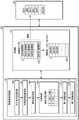
控制器130可以包括存储器144和高速缓存控制器145。如上面参照图1所述,控制器130可以包括主机接口电路132、处理器134和存储器接口电路142。然而,为清楚起见,图4A和图4B省略了这些组件。可以由处理器134驱动高速缓存控制器145。高速缓存控制器145可以包括写入命令接收电路1450、可用空间检查电路1451、模式确定电路1452、计数电路1453、LBA生成电路1454和更新电路1455。
如在本公开中所使用的,术语“电路”可以指代以下所有:(a)仅硬件电路的实施方案(诸如仅模拟和/或数字电路的实施方案)和(b)电路和软件(和/或固件)的组合,诸如(可适用的):(i)(一个或多个)处理器的组合或(ii)一起工作以使诸如移动电话或服务器的设备执行各种功能的(一个或多个)处理器/软件(包括数字信号处理器)、软件和存储器的部分,以及(c)需要软件或固件来进行操作(即使该软件或固件并非物理存在)的电路,诸如,(一个或多个)微处理器或(一个或多个)微处理器的一部分。“电路”的这种定义适用于该术语在本申请中的所有应用中,包括在任意权利要求中的应用。作为另外的示例,如在本申请中所使用的,术语“电路”还将涵盖仅处理器(或多个处理器)或处理器的一部分及其(或它们)附带的软件和/或固件的实施方案。如果术语“电路”适用于特定的权利要求要素,则“电路”例如还将涵盖用于存储装置的集成电路。As used in this disclosure, the term "circuitry" may refer to all of: (a) hardware-only circuit implementations (such as analog and/or digital-only circuit implementations) and (b) circuitry and software (and and/or firmware) such as (applicable): (i) a combination of (one or more) processors or (ii) a combination of (one or more) multiple) processors/software (including digital signal processors), portions of software and memory, and (c) circuits that require software or firmware to operate (even if such software or firmware is not physically present), such as, (one or Multiple) microprocessor(s) or part of a microprocessor(s). This definition of 'circuitry' applies to all uses of this term in this application, including in any claims. As a further example, as used in this application, the term "circuitry" would also cover an implementation of merely a processor (or multiple processors) or a portion thereof and its (or their) accompanying software and/or firmware. implementation plan. If the term "circuitry" applies to a particular claim element, "circuitry" would also cover integrated circuits for memory devices, for example.
参照图4A,写入命令接收电路1450可以从命令队列52请求包括多条命令信息的命令信息,并且从命令队列接收所请求的一条或多条命令信息。例如,多条命令信息可以包括写入命令或读取命令。此外,多条命令信息可以包括写入命令。并且,多条命令信息可以包括第一写入命令至第四写入命令。写入命令接收电路1450可以从命令队列请求第一写入命令,并且接收第一写入命令。Referring to FIG. 4A , the write
为了将包括在通过写入命令接收电路1450接收的第一写入命令中的写入LBA信息写入到与第零映射段S0对应的区域(或映射段区域),可用空间检查电路1451可以检查与第零映射段S0对应的映射段区域的可用空间。可用空间检查电路1451可以通过检查是否以第零映射段S0的大小将LBA信息写入到与第零映射段S0对应的映射段区域来检查与第零映射段S0对应的映射段区域的可用空间。换言之,可用空间检查电路1451可以通过检查在第二LBA信息之前写入的第一LBA信息的位置是否指示分配到与第零映射段S0对应的映射段区域的Max_INDEX(例如,1023)来检查与第零映射段S0对应的映射段区域的可用空间。当检查结果显示写入第一LBA信息的位置不指示与第零映射段S0对应的映射段区域的Max_INDEX时,与第一写入命令对应的第二LBA信息可以通过更新电路1455存储在与第零映射段S0对应的映射段区域中,这将在下面描述。另一方面,当检查结果显示写入第一LBA信息的位置指示与第零映射段S0对应的映射段区域的Max_INDEX时,可用空间检查电路1451可以确定与第零映射段S0对应的映射段区域没有写入第二LBA信息的可用空间。此处,为了减少通过更新电路1455更新存储器装置150的操作次数,模式确定电路1452确定第一LBA信息和第二LBA信息的模式,而不将第零映射段S0更新到存储器装置150。In order to write the write LBA information included in the first write command received by the write
模式确定电路1452可以确定被写入到与第零映射段S0对应的映射段区域的Max_INDEX的第一LBA信息和与第一写入命令对应的当前待写入的第二LBA信息的模式。The
由于模式确定电路1452的确定结果指示第一LBA信息和第二LBA信息是顺序的,因此计数电路1453增大顺序计数信息,并将增加的顺序计数信息存储在顺序计数列表中。顺序计数列表可以包括映射段信息“S”、存储在与映射段对应的映射段区域的索引Max_INDEX中的LBA信息“LBA”和顺序LBA计数“COUNT”。例如,如图4A所示,顺序计数列表显示映射段信息“S”可以包括第零映射段(0),LBA信息“LBA”可以包括LBA1001,并且顺序LBA计数“COUNT”可以是3。Since the determination result of the
更具体地,当写入到与第零映射段S0对应的映射段区域的Max_INDEX的第一LBA信息是LBA1001,并且与第一写入命令对应的第二LBA信息是LBA1002时,模式确定电路1452确定第一LBA信息和第二LBA信息的模式是顺序模式。而且,通过计数电路1453,顺序LBA计数“COUNT”可以为1。More specifically, when the first LBA information written to the Max_INDEX of the mapping segment area corresponding to the zeroth mapping segment S0 is LBA1001, and the second LBA information corresponding to the first write command is LBA1002, the
因为LBA1001和LBA1002的模式是顺序模式,所以模式确定电路1452确定包括在通过写入命令接收电路1450从命令队列接收的第二写入命令、第三写入命令和第四写入命令中的LBA信息的模式。例如,当由于包括在第一写入命令中的第一LBA信息是LBA1002并且包括在第二写入命令中的第二LBA信息是LBA1003因而第一LBA信息和第二LBA信息的模式被确定是顺序模式时,计数电路1453可以将顺序LBA计数“COUNT”从1增大至2。随后,当由于包括在第二写入命令中的第一LBA信息是LBA1003并且包括在第三写入命令中的第二LBA信息是LBA1004因而第一LBA信息和第二LBA信息的模式被确定是顺序模式时,计数电路1453可以将顺序LBA计数“COUNT”从2增大至3。Since the modes of the
随后,当由于包括在第三写入命令中的第一LBA信息是LBA1004并且包括在第四写入命令中的第二LBA信息是LBA1030因而第一LBA信息和第二LBA信息的模式被确定是随机模式时,计数电路1453不执行计数操作,而是LBA生成电路1454和更新电路1455进行操作。Subsequently, when the modes of the first LBA information and the second LBA information are determined to be because the first LBA information included in the third write command is LBA1004 and the second LBA information included in the fourth write command is LBA1030 In the random mode, the
LBA生成电路1454基于顺序计数列表生成一条或多条LBA信息。例如,可以看出,在LBA1001被写入到与第零映射段S0对应的映射段区域的Max_INDEX之后的顺序LBA计数“COUNT”是3。换言之,当能够存储一个LBA信息的大小是4KB时,LBA生成电路1454可以计算待另外生成的LBA信息的大小为COUNT*4KB。也就是说,由于顺序LBA计数“COUNT”是3,因此可以计算出12KB。The
更新电路1455通过将由LBA生成电路1454生成的LBA信息添加到第零映射段S0来可变地调整第零映射段S0的大小,并且将第零映射段S0更新到存储器装置150。换言之,更新电路1455可以将第零映射段S0的大小12KB与另外生成的LBA信息的大小12KB合并以更新存储器装置150,从而减少更新次数。The
在各个实施例中,当以分配给第零映射段S0或与第零映射段S0对应的映射段区域的大小写入多条LBA信息时,高速缓存控制器145不更新第零映射段S0,而是确定写入到与第零映射段S0对应的映射段区域的Max_Index的第一LBA信息和待写入的第二LBA信息的模式。第一LBA信息包括先前LBA信息,第二LBA信息包括从当前命令队列传送以被写入的LBA信息。当确定结果指示这样的第一LBA信息和第二LBA信息是顺序模式时,高速缓存控制器145对顺序LBA信息进行计数,直到第一LBA信息和第二LBA信息的模式被确定是随机模式。换言之,每当第一LBA信息和第二LBA信息的模式被确定是顺序模式时,高速缓存控制器145可以增加顺序计数。高速缓存控制器145可以通过顺序计数生成一条或多条LBA信息,并且将生成的LBA信息另外合并到第零映射段中,从而更新存储器装置150。换言之,高速缓存控制器145可以通过可变地调整第零映射段S0的大小来更新存储器装置150。In various embodiments, when writing multiple pieces of LBA information with the size allocated to the zeroth mapping segment S0 or the mapping segment area corresponding to the zeroth mapping segment S0, the
参照图4B,写入命令接收电路1450可以从命令队列请求包括多条命令信息的命令信息,并且从命令队列接收所请求的一条或多条命令信息。例如,多条命令信息可以包括写入命令或读取命令。此外,多条命令信息可以包括写入命令。并且,多条命令信息可以包括第一写入命令至第四写入命令。写入命令接收电路1450可以向命令队列请求第一写入命令,并且从命令队列接收第一写入命令。Referring to FIG. 4B , the write
为了将包括在通过写入命令接收电路1450接收的第一写入命令中的LBA信息写入到与第零映射段S0对应的存储器144的映射段区域,可用空间检查电路1451可以检查与第零映射段S0对应的映射段区域的可用空间。可用空间检查电路1451可以通过检查是否以第零映射段S0的大小将LBA信息写入到与第零映射段S0对应的映射段区域来检查与第零映射段S0对应的映射段区域的可用空间。换言之,可用空间检查电路1451可以通过检查在第二LBA信息之前写入的第一LBA信息的位置是否指示分配到与第零映射段S0对应的映射段区域的Max_INDEX(例如,1023)来检查第零映射段S0的可用空间。当检查结果显示写入第一LBA信息的位置不指示与第零映射段S0对应的映射段区域的Max_INDEX时,与第一写入命令对应的第二LBA信息可以通过更新电路1455存储在与第零映射段S0对应的映射段区域中,这将在下面描述。另一方面,当检查结果显示写入第一LBA信息的位置指示第零映射段S0的Max_INDEX时,可用空间检查电路1451可以确定与第零映射段S0对应的映射段区域没有可以写入第二LBA信息的可用空间。此处,为了减少通过更新电路1455更新存储器装置150的操作次数,模式确定电路1452确定第一LBA信息和第二LBA信息的模式,而不将第零映射段S0更新到存储器装置150。In order to write the LBA information included in the first write command received by the write
模式确定电路1452可以确定被写入到与第零映射段S0对应的映射段区域的Max_INDEX的第一LBA信息和与第一写入命令对应的当前待写入的第二LBA信息的模式。例如,当写入到与第零映射段S0对应的映射段区域的Max_INDEX的第一LBA信息是LBA1001,并且与第一写入命令对应的第二LBA信息是LBA1030时,模式确定电路1452确定第一LBA信息和第二LBA信息的模式是随机模式。The
更新电路1455可以将包括在第零映射段S0中的多条LBA信息更新到存储器装置150,并且与第一写入命令对应的LBA1030可被写入到第一映射段。The
图5是示意性地示出根据第二实施例的存储器系统的示图。FIG. 5 is a diagram schematically showing a memory system according to a second embodiment.
参照图5,存储器系统110可以包括控制器130和存储器装置150。Referring to FIG. 5 , the
控制器130可以包括存储器144和高速缓存控制器145。如上面参照图1所述,控制器130可以包括主机接口电路132、处理器134和存储器接口电路142。然而,为清楚起见,在图5中省略了这些组件。高速缓存控制器145可以由处理器134驱动。高速缓存控制器145可以包括写入命令接收电路1450、可用空间检查电路1451、模式确定电路1452、计数电路1453、以及第一更新电路1455_1和第二更新电路和1455_2。
参照图5,由于写入命令接收电路1450、可用空间检查电路1451、模式确定电路1452和计数电路1453与以上根据第一实施例描述的相同,所以省略对其的描述。下面描述第一更新电路1455_1和第二更新电路和1455_2。Referring to FIG. 5, since the write
模式确定电路1452确定第一LBA信息和第二LBA信息是顺序模式之后,当通过写入命令接收电路1450从命令队列接收的LBA信息是随机LBA信息时,第一更新电路1455_1仅将包括在第零映射段S0中的多条LBA信息更新到存储器装置150。换言之,第一更新电路1455_1仅将是第零映射段S0的大小(例如,18KB)的LBA信息更新到存储器装置150。随后,第一更新电路1455_1通过删除第零映射段S0的信息将第零映射段S0改变成第一映射段S1。换言之,第零映射段S0和第一映射段S1是相同的区域。After the
第二更新电路1455_2可以通过基于存储在计数电路1453中的顺序计数列表生成与LBA计数对应的LBA信息并将生成的LBA信息写入与第一映射段S1对应的映射段区域来执行更新。The second update circuit 1455_2 may perform update by generating LBA information corresponding to the LBA count based on the sequential count list stored in the
图6是用于描述根据第一实施例的存储器系统110的操作方法的流程图。可以由包括图1和图4A-图4B的高速缓存控制器145的存储器系统110执行图6的操作方法。FIG. 6 is a flowchart for describing an operating method of the
参照图6,在步骤S601中,高速缓存控制器145可以从命令队列请求包括多条命令信息的命令信息,并且从命令队列接收所请求的一条或多条命令信息。例如,多条命令信息可以包括写入命令或读取命令。此外,多条命令信息可以包括写入命令。而且,多条命令信息可以包括第一写入命令至第四写入命令。高速缓存控制器145可以从命令队列请求并顺序地接收写入命令。Referring to FIG. 6, in step S601, the
在步骤S603和S605中,为了将包括在第一写入命令中的LBA信息写入到与第零映射段S0对应的映射段区域,高速缓存控制器145可以检查与第零映射段S0对应的区域(即,映射段区域)的可用空间。高速缓存控制器145可以通过检查是否以第零映射段S0的大小将LBA信息写入到与第零映射段S0对应的映射段区域来检查与第零映射段S0对应的映射段区域的可用空间。换言之,高速缓存控制器145可以通过检查在第二LBA信息之前写入的第一LBA信息的位置是否指示分配至与第零映射段S0对应的映射段区域的Max_INDEX来检查与第零映射段S0对应的映射段区域的可用空间。In steps S603 and S605, in order to write the LBA information included in the first write command into the mapping segment area corresponding to the zeroth mapping segment S0, the
当检查结果显示写入第一LBA信息的位置不指示与第零映射段S0对应的映射段区域的Max_INDEX(即,步骤S605为“否”)时,在步骤S607中,高速缓存控制器145可以将与第一写入命令对应的第二LBA信息写入到与第零映射段S0对应的映射段区域。另一方面,当检查结果显示写入第一LBA信息的位置指示与第零映射段S0对应的映射段区域的Max_INDEX(即,步骤S605为“是”)时,在步骤S609和S611中,高速缓存控制器145可以确定被写入到与第零映射段S0对应的映射段区域的Max_INDEX的第一LBA信息和与第一写入命令对应的当前待写入的第二LBA信息的模式。When the check result shows that the position where the first LBA information is written does not indicate the Max_INDEX of the mapping segment area corresponding to the zeroth mapping segment S0 (that is, "No" in step S605), in step S607, the
当确定结果指示第一LBA信息和第二LBA信息的模式是顺序模式(即,步骤S611为“是”)时,在步骤S613中,高速缓存控制器145可以增大顺序计数。例如,如图4A所示,当写入到与第零映射段S0对应的映射段区域的Max_INDEX的第一LBA信息是LBA1001,并且与第一写入命令对应的第二LBA信息是LBA1002时,高速缓存控制器145可以确定第一LBA信息和第二LBA信息的模式是顺序模式,并且增大顺序计数。当重复执行步骤S601至S609设定或预定次数直到第一LBA信息和第二LBA信息的模式变为随机模式时,可以在每次迭代时增大顺序计数。When the determination result indicates that the mode of the first LBA information and the second LBA information is a sequential mode (ie, YES in step S611), in step S613, the
另一方面,如图4B所示,当确定结果指示第一LBA信息和第二LBA信息的模式是随机模式(即,步骤S611为“否”)时,在步骤S617中,高速缓存控制器145可以检查顺序计数列表,然后在顺序计数列表没有计数信息的情况下,仅将被写入到与第零映射段对应的映射段区域的多条LBA信息更新到存储器装置150中。On the other hand, as shown in FIG. 4B, when the determination result indicates that the pattern of the first LBA information and the second LBA information is a random pattern (that is, "No" in step S611), in step S617, the
在步骤S617中,当顺序计数列表的检查结果显示顺序计数列表具有计数信息时,高速缓存控制器145可以基于计数信息,生成与写入到与第零映射段S0对应的映射段区域的Max_INDEX的LBA信息连续的一条或多条LBA信息。随后,高速缓存控制器145可以将所生成的一条或多条LBA信息与第零映射段S0合并,从而更新存储器装置150。In step S617, when the check result of the sequence count list shows that the sequence count list has count information, the
图7是示出根据第二实施例的存储器系统的操作方法的流程图。可以由包括图1和5的高速缓存控制器145的存储器系统110执行图7的操作方法。FIG. 7 is a flowchart showing an operating method of the memory system according to the second embodiment. The method of operation of FIG. 7 may be performed by the
参照图7,由于步骤S701至S713与上面参照图6描述的步骤S601至S613相同,因此省略其描述。Referring to FIG. 7 , since steps S701 to S713 are the same as steps S601 to S613 described above with reference to FIG. 6 , description thereof is omitted.
在步骤S717中,当步骤S711的确定结果指示第一LBA信息和第二LBA信息的模式是随机模式时,高速缓存控制器145可以检查顺序计数列表。当顺序计数列表没有计数信息时,高速缓存控制器145可以仅将写入到与第零映射段对应的映射段区域的多条LBA信息更新到存储器装置150。另一方面,当顺序计数列表具有计数信息时,在步骤S719中,高速缓存控制器145可以仅将写入到与第零映射段对应的映射段区域的多条LBA信息更新到存储器装置150,并且然后删除写入到与第零映射段对应的映射段区域的多条LBA信息。在步骤S721中,高速缓存控制器145可以将第零映射段改变为第一映射段。在步骤S723中,高速缓存控制器145可以基于计数信息,生成与写入到与第零映射段S0对应的映射段区域的Max_INDEX的LBA信息连续的一条或多条LBA信息,并且将所生成的LBA信息写入到第一映射段中。In step S717, when the determined result of step S711 indicates that the pattern of the first LBA information and the second LBA information is a random pattern, the
图8是示出根据实施例的存储器系统中使用的超级存储块的概念的示图。FIG. 8 is a diagram illustrating the concept of a super block used in a memory system according to an embodiment.
图8示出在根据实施例的存储器系统110的组件之中、包括在图1的存储器装置150中的多个存储器管芯1501至150n。例如,存储器装置150可以包括第一存储器管芯1501和第二存储器管芯1502。FIG. 8 illustrates a plurality of memory dies 1501 to 150 n included in the
第一存储器管芯1501和第二存储器管芯1502中的每一个可以包括多个平面。例如,第一存储器管芯1501可以包括第一平面PLANE00和第二平面PLANE01,第二存储器管芯1502可以包括第三平面PLANE10和第四平面PLANE11。平面中的每一个可以包括多个块。例如,第一平面PLANE00可以包括第一至第N存储块BLOCK000至BLCOK00N,第二平面PLANE01可以包括第一至第N存储块BLOCK010至BLCOK01N。第三平面PLANE10可以包括第一至第N存储块BLOCK100至BLCOK10N,第四平面PLANE11可以包括第一至第N存储块BLOCK110至BLCOK11N。Each of the
第一存储器管芯1501能够通过第零通道CH0输入/输出数据,第二存储器管芯1502能够通过第一通道CH1输入/输出数据。第零通道CH0和第一通道CH1可以交织方案输入/输出数据。The first memory die 1501 can input/output data through the zeroth channel CH0, and the second memory die 1502 can input/output data through the first channel CH1. The zeroth channel CH0 and the first channel CH1 can input/output data in an interleaving scheme.
第一存储器管芯1501包括分别与多个通路WAY0和WAY1对应的多个平面PLANE00和PLANE01,该通路WAY0和WAY1能够通过共享第零通道CH0以交织方案输入/输出数据。The first memory die 1501 includes a plurality of planes PLANE00 and PLANE01 respectively corresponding to a plurality of ways WAY0 and WAY1 capable of inputting/outputting data in an interleaved scheme by sharing a zeroth channel CH0 .
第二存储器管芯1502包括分别与多个通路WAY2和WAY3对应的多个平面PLANE10和PLANE11,该通路WAY2和WAY3能够通过共享第一通道CH1以交织方案输入/输出数据。The second memory die 1502 includes a plurality of planes PLANE10 and PLANE11 respectively corresponding to a plurality of ways WAY2 and WAY3 capable of inputting/outputting data in an interleaved scheme by sharing the first channel CH1.
可以基于使用相同通路或通道的物理位置将存储器装置150中的多个存储块划分成组。Multiple memory blocks in
虽然图8的实施例示出存在两个管芯,每个管芯具有两个平面的存储器装置150的配置,但是本发明不限于这种配置。可以基于系统设计考虑使用任何合适的管芯和平面配置。每个平面中的存储块的数量也可以变化。Although the embodiment of FIG. 8 shows a configuration in which there are two dies, each having two planes of
控制器130可以基于存储块的物理位置对不同管芯或不同平面中的多个存储块之中、能够被同时选择的多个存储块进行分组,并且将存储块组作为超级存储块进行管理。The
可以根据设计者的选择以各种方式执行控制器130将存储块分组为超级存储块并管理超级存储块的方案。下面描述三个示例性方案。A scheme in which the
第一种方案是控制器130将存储器装置150中的多个存储器管芯1501和1502中的第一存储器管芯1501的第一平面PLANE00的任意存储块BLOCK000和第二平面PLANE01的任意存储块BLOCK010进行分组,并且将分组的存储块BLOCK000和BLOCK010作为单个超级存储块A1进行管理。当第一方案被应用到存储器装置150中的第二存储器管芯1502时,控制器130可以将第二存储器管芯1502的第一平面PLANE10的任意存储块BLOCK100和第二平面PLANE11的任意存储块BLOCK110进行分组,并且将分组的存储块BLOCK100和BLOCK110作为单个超级存储块A2进行管理。The first solution is that the
第二种方案是控制器130将第一存储器管芯1501的第一平面PLANE00的任意存储块BLOCK002和第二存储器管芯1502的第一平面PLANE10的任意存储块BLOCK102进行分组,并且将分组的存储块BLOCK002和BLOCK102作为单个超级存储块B1来管理。另外,根据第二种方案,控制器130将第一存储器管芯1501的第二平面PLANE01的任意存储块BLOCK012和第二存储器管芯1502的第二平面PLANE11的任意存储块BLOCK112进行分组,并且将分组的存储块BLOCK012和BLOCK112作为单个超级存储块B2进行管理The second scheme is that the
第三种方案是控制器130将第一存储器管芯1501的第一平面PLANE00的任意存储块BLOCK001、第一存储器管芯1501的第二平面PLANE01的任意存储块BLOCK011、第二存储器管芯1502的第一平面PLANE10的任意存储块BLOCK101、第二存储器管芯1502的第二平面PLANE11中的任意存储块BLOCK111进行分组,并且将分组的存储块BLOCK001、BLOCK011、BLOCK101和BLOCK111作为单个超级存储块C进行管理。The third scheme is that the
因此,可以通过交织方案,例如通道交织方案、存储器管芯交织方案、存储器芯片交织方案或通路交织方案基本上同时选择包括在超级存储块中的每一个的可同时选择的存储块。Accordingly, simultaneously selectable memory blocks included in each of the super memory blocks may be selected substantially simultaneously by an interleaving scheme, such as a channel interleaving scheme, a memory die interleaving scheme, a memory chip interleaving scheme, or a lane interleaving scheme.
根据本发明的实施例,基于第一LBA信息和第二LBA信息的模式,映射段的大小可以被可变地调整并更新到存储器装置,从而减少对存储器装置的更新次数。According to an embodiment of the present invention, based on the patterns of the first LBA information and the second LBA information, the size of the mapping segment may be variably adjusted and updated to the memory device, thereby reducing the number of updates to the memory device.
虽然针对特定实施例已经说明并描述了本发明,但是根据前面的描述,本领域技术人员将显而易见的是,在不脱离如以下权利要求所限定的本发明的精神和范围的情况下,可以进行各种改变和修改。While the invention has been illustrated and described with respect to particular embodiments, it will be apparent to those skilled in the art from the foregoing description that other modifications may be made without departing from the spirit and scope of the invention as defined in the following claims. Various changes and modifications.
Claims (19)
Applications Claiming Priority (2)
| Application Number | Priority Date | Filing Date | Title |
|---|---|---|---|
| KR1020180124324AKR102679985B1 (en) | 2018-10-18 | 2018-10-18 | Memory system and method of operation of the memory system |
| KR10-2018-0124324 | 2018-10-18 |
Publications (2)
| Publication Number | Publication Date |
|---|---|
| CN111078582A CN111078582A (en) | 2020-04-28 |
| CN111078582Btrue CN111078582B (en) | 2023-03-24 |
Family
ID=70279149
Family Applications (1)
| Application Number | Title | Priority Date | Filing Date |
|---|---|---|---|
| CN201910634998.3AActiveCN111078582B (en) | 2018-10-18 | 2019-07-15 | Memory system based on mode adjustment mapping segment and operation method thereof |
Country Status (3)
| Country | Link |
|---|---|
| US (1) | US10860231B2 (en) |
| KR (1) | KR102679985B1 (en) |
| CN (1) | CN111078582B (en) |
Families Citing this family (12)
| Publication number | Priority date | Publication date | Assignee | Title |
|---|---|---|---|---|
| KR102767981B1 (en)* | 2018-11-14 | 2025-02-17 | 에스케이하이닉스 주식회사 | Memory system having cache system and method of controlling caching operation in the memory system |
| KR20210012820A (en) | 2019-07-26 | 2021-02-03 | 에스케이하이닉스 주식회사 | Memory controller and operating method thereof |
| US11838222B2 (en) | 2019-12-21 | 2023-12-05 | Western Digital Technologies, Inc. | In-line data identification on network |
| US11297010B2 (en)* | 2019-12-23 | 2022-04-05 | Western Digital Technologies, Inc. | In-line data operations for storage systems |
| US11543987B2 (en)* | 2020-06-04 | 2023-01-03 | Western Digital Technologies, Inc. | Storage system and method for retention-based zone determination |
| KR102848213B1 (en)* | 2020-10-05 | 2025-08-21 | 에스케이하이닉스 주식회사 | Host device, Data storage device, Data processing system and Data processing method |
| WO2022204915A1 (en) | 2021-03-30 | 2022-10-06 | Yangtze Memory Technologies Co., Ltd. | Pattern generation system with pin function mapping |
| US12321620B2 (en)* | 2021-08-06 | 2025-06-03 | Micron Technology, Inc. | Techniques for memory zone size adjustment |
| JP2023044521A (en)* | 2021-09-17 | 2023-03-30 | キオクシア株式会社 | memory system |
| US12056048B2 (en)* | 2021-11-11 | 2024-08-06 | Samsung Electronics Co., Ltd. | System and method for management of electronic memory |
| US20230418743A1 (en)* | 2021-12-28 | 2023-12-28 | SK Hynix Inc. | Data storage device and method of operating the same |
| KR20230139153A (en) | 2022-03-25 | 2023-10-05 | 에스케이하이닉스 주식회사 | Storage device including memory controller and operating method thereof |
Family Cites Families (18)
| Publication number | Priority date | Publication date | Assignee | Title |
|---|---|---|---|---|
| US20090193184A1 (en)* | 2003-12-02 | 2009-07-30 | Super Talent Electronics Inc. | Hybrid 2-Level Mapping Tables for Hybrid Block- and Page-Mode Flash-Memory System |
| US8601223B1 (en)* | 2006-09-19 | 2013-12-03 | Nvidia Corporation | Techniques for servicing fetch requests utilizing coalesing page table entries |
| KR100843135B1 (en)* | 2006-11-20 | 2008-07-02 | 삼성전자주식회사 | Non-volatile memory management method and device |
| US8516221B2 (en)* | 2008-10-31 | 2013-08-20 | Hewlett-Packard Development Company, L.P. | On-the fly TLB coalescing |
| KR101662827B1 (en) | 2010-07-02 | 2016-10-06 | 삼성전자주식회사 | Memory system selecting write mode of data block and data write method thereof |
| US20140244901A1 (en)* | 2013-02-26 | 2014-08-28 | Lsi Corporation | Metadata management for a flash drive |
| KR20140113176A (en)* | 2013-03-15 | 2014-09-24 | 삼성전자주식회사 | Method for performing update of mapping information and memory system using method thereof |
| US20150331624A1 (en)* | 2014-05-19 | 2015-11-19 | Kabushiki Kaisha Toshiba | Host-controlled flash translation layer snapshot |
| KR20160027805A (en)* | 2014-09-02 | 2016-03-10 | 삼성전자주식회사 | Garbage collection method for non-volatile memory device |
| KR102329924B1 (en)* | 2015-10-27 | 2021-11-23 | 삼성전자 주식회사 | Electronic device for managing a memory and method thereof |
| TWI579693B (en)* | 2016-04-29 | 2017-04-21 | 群聯電子股份有限公司 | Mapping table loading method, memory control circuit unit and mempry storage apparatus |
| KR102611292B1 (en) | 2016-06-22 | 2023-12-11 | 에스케이하이닉스 주식회사 | Memory system and operating method of memory system |
| KR20180041898A (en)* | 2016-10-17 | 2018-04-25 | 에스케이하이닉스 주식회사 | Memory system and operating method of memory system |
| KR102761231B1 (en)* | 2016-10-27 | 2025-02-05 | 에스케이하이닉스 주식회사 | Memory system and operating method thereof |
| JP2018160059A (en)* | 2017-03-22 | 2018-10-11 | 東芝メモリ株式会社 | Memory controller |
| US10459636B2 (en)* | 2017-03-24 | 2019-10-29 | Sandisk Technologies Llc | System and method for managing data in non-volatile memory systems having multiple mapping layers |
| KR102687593B1 (en)* | 2018-03-12 | 2024-07-24 | 에스케이하이닉스 주식회사 | Controller and operation method thereof |
| KR20200013897A (en)* | 2018-07-31 | 2020-02-10 | 에스케이하이닉스 주식회사 | Controller and operation method thereof |
- 2018
- 2018-10-18KRKR1020180124324Apatent/KR102679985B1/enactiveActive
- 2019
- 2019-05-09USUS16/408,221patent/US10860231B2/enactiveActive
- 2019-07-15CNCN201910634998.3Apatent/CN111078582B/enactiveActive
Also Published As
| Publication number | Publication date |
|---|---|
| US10860231B2 (en) | 2020-12-08 |
| CN111078582A (en) | 2020-04-28 |
| KR102679985B1 (en) | 2024-07-02 |
| KR20200043676A (en) | 2020-04-28 |
| US20200125261A1 (en) | 2020-04-23 |
Similar Documents
| Publication | Publication Date | Title |
|---|---|---|
| CN111078582B (en) | Memory system based on mode adjustment mapping segment and operation method thereof | |
| CN111240586B (en) | Memory system and method of operating the same | |
| US11030094B2 (en) | Apparatus and method for performing garbage collection by predicting required time | |
| KR102559549B1 (en) | Apparatus and method for managing block status in memory system | |
| US11392309B2 (en) | Memory system for performing migration operation and operating method thereof | |
| KR102743227B1 (en) | Memory system and operating method thereof | |
| KR20200019431A (en) | Controller and operating method thereof | |
| KR20200059936A (en) | Memory system and operation method thereof | |
| KR20200019421A (en) | Apparatus and method for checking valid data in block capable of large volume data in memory system | |
| KR102595233B1 (en) | Data processing system and operating method thereof | |
| CN119718200A (en) | Operations based on integrated memory region description data | |
| CN115080457A (en) | Controller and operation method thereof | |
| KR102750797B1 (en) | Apparatus and method for performing garbage collection to predicting required time | |
| CN115543860A (en) | Data processing system and method of operation thereof | |
| CN111352858B (en) | Memory system and method of operation thereof | |
| CN109407968B (en) | Memory system and operating method thereof | |
| US11656996B2 (en) | Controller for managing order information of data, operation method thereof, and memory system including the same | |
| CN113918084B (en) | Memory system and method of operating the same | |
| US11657000B2 (en) | Controller and memory system including the same | |
| US20220164119A1 (en) | Controller, and memory system and data processing system including the same | |
| CN111290971B (en) | Controller, memory system having same, and method of operating memory system | |
| US20250173060A1 (en) | Managing namespace mapping in a memory sub-system | |
| US11586382B2 (en) | Memory system and data processing system for distributedly storing input data |
Legal Events
| Date | Code | Title | Description |
|---|---|---|---|
| PB01 | Publication | ||
| PB01 | Publication | ||
| SE01 | Entry into force of request for substantive examination | ||
| SE01 | Entry into force of request for substantive examination | ||
| GR01 | Patent grant | ||
| GR01 | Patent grant | ||
| TR01 | Transfer of patent right | Effective date of registration:20240613 Address after:American Texas Patentee after:Mimi IP Co.,Ltd. Country or region after:U.S.A. Address before:Gyeonggi Do, South Korea Patentee before:Sk Hynix Inc. Country or region before:Republic of Korea | |
| TR01 | Transfer of patent right |