CN111029335B - deep ultraviolet light-emitting device - Google Patents
deep ultraviolet light-emitting deviceDownload PDFInfo
- Publication number
- CN111029335B CN111029335BCN201911328889.5ACN201911328889ACN111029335BCN 111029335 BCN111029335 BCN 111029335BCN 201911328889 ACN201911328889 ACN 201911328889ACN 111029335 BCN111029335 BCN 111029335B
- Authority
- CN
- China
- Prior art keywords
- deep ultraviolet
- substrate
- light
- emitting device
- optical lens
- Prior art date
- Legal status (The legal status is an assumption and is not a legal conclusion. Google has not performed a legal analysis and makes no representation as to the accuracy of the status listed.)
- Active
Links
Images


Classifications
- H—ELECTRICITY
- H10—SEMICONDUCTOR DEVICES; ELECTRIC SOLID-STATE DEVICES NOT OTHERWISE PROVIDED FOR
- H10H—INORGANIC LIGHT-EMITTING SEMICONDUCTOR DEVICES HAVING POTENTIAL BARRIERS
- H10H20/00—Individual inorganic light-emitting semiconductor devices having potential barriers, e.g. light-emitting diodes [LED]
- H10H20/80—Constructional details
- H10H20/85—Packages
- H10H20/8506—Containers
- H—ELECTRICITY
- H01—ELECTRIC ELEMENTS
- H01L—SEMICONDUCTOR DEVICES NOT COVERED BY CLASS H10
- H01L25/00—Assemblies consisting of a plurality of semiconductor or other solid state devices
- H01L25/03—Assemblies consisting of a plurality of semiconductor or other solid state devices all the devices being of a type provided for in a single subclass of subclasses H10B, H10D, H10F, H10H, H10K or H10N, e.g. assemblies of rectifier diodes
- H01L25/04—Assemblies consisting of a plurality of semiconductor or other solid state devices all the devices being of a type provided for in a single subclass of subclasses H10B, H10D, H10F, H10H, H10K or H10N, e.g. assemblies of rectifier diodes the devices not having separate containers
- H01L25/075—Assemblies consisting of a plurality of semiconductor or other solid state devices all the devices being of a type provided for in a single subclass of subclasses H10B, H10D, H10F, H10H, H10K or H10N, e.g. assemblies of rectifier diodes the devices not having separate containers the devices being of a type provided for in group H10H20/00
- H01L25/0753—Assemblies consisting of a plurality of semiconductor or other solid state devices all the devices being of a type provided for in a single subclass of subclasses H10B, H10D, H10F, H10H, H10K or H10N, e.g. assemblies of rectifier diodes the devices not having separate containers the devices being of a type provided for in group H10H20/00 the devices being arranged next to each other
- H—ELECTRICITY
- H10—SEMICONDUCTOR DEVICES; ELECTRIC SOLID-STATE DEVICES NOT OTHERWISE PROVIDED FOR
- H10H—INORGANIC LIGHT-EMITTING SEMICONDUCTOR DEVICES HAVING POTENTIAL BARRIERS
- H10H20/00—Individual inorganic light-emitting semiconductor devices having potential barriers, e.g. light-emitting diodes [LED]
- H10H20/80—Constructional details
- H10H20/85—Packages
- H10H20/855—Optical field-shaping means, e.g. lenses
- H—ELECTRICITY
- H10—SEMICONDUCTOR DEVICES; ELECTRIC SOLID-STATE DEVICES NOT OTHERWISE PROVIDED FOR
- H10H—INORGANIC LIGHT-EMITTING SEMICONDUCTOR DEVICES HAVING POTENTIAL BARRIERS
- H10H20/00—Individual inorganic light-emitting semiconductor devices having potential barriers, e.g. light-emitting diodes [LED]
- H10H20/80—Constructional details
- H10H20/85—Packages
- H10H20/857—Interconnections, e.g. lead-frames, bond wires or solder balls
Landscapes
- Engineering & Computer Science (AREA)
- Power Engineering (AREA)
- Microelectronics & Electronic Packaging (AREA)
- Physics & Mathematics (AREA)
- Condensed Matter Physics & Semiconductors (AREA)
- General Physics & Mathematics (AREA)
- Computer Hardware Design (AREA)
- Led Device Packages (AREA)
Abstract
Translated fromChinese
Description
Translated fromChinese技术领域technical field
本发明涉及LED技术领域,尤其涉及一种深紫外发光装置。The present invention relates to the field of LED technology, in particular to a deep ultraviolet light emitting device.
背景技术Background technique
发光二极管(Light Emitting Diode,以下简称LED)包括紫外LED,紫外LED一般指发光中心波长在400nm以下的LED,发光波长大于380nm时称为近紫外LED,短于300nm时称为深紫外LED,深紫外发光LED在杀菌消毒、聚合物固化、生化探测、非视距通讯及特种照明等领域有着广阔的应用前景。相较于传统的紫外光源汞灯,深紫外发光二极管具有环保、小巧便携、低功耗等诸多优点,受到越来越多的关注和重视。Light-emitting diodes (Light Emitting Diode, hereinafter referred to as LED) include ultraviolet LEDs. Ultraviolet LEDs generally refer to LEDs with a central wavelength of light below 400nm. When the light-emitting wavelength is greater than 380nm, it is called near-ultraviolet LED, and when it is shorter than 300nm, it is called deep-UV LED. Ultraviolet LEDs have broad application prospects in the fields of sterilization, polymer curing, biochemical detection, non-line-of-sight communication and special lighting. Compared with the traditional ultraviolet light source mercury lamp, the deep ultraviolet light emitting diode has many advantages such as environmental protection, compactness and portability, low power consumption, etc., and has received more and more attention and attention.
传统的深紫外发光装置中,深紫外LED芯片通常封装在壳体内形成封装元件,多个封装元件二次焊接在基板上。二次焊接封装元件时,容易影响封装元件中深紫外LED芯片的性能,或导致封装元件开裂,可靠性差,而且多次封装会影响紫外光线的释出,导致紫外光取出效率低。In the traditional deep ultraviolet light-emitting device, the deep ultraviolet LED chip is usually packaged in a casing to form a package component, and a plurality of package components are secondary welded on the substrate. When the packaged components are soldered for the second time, it is easy to affect the performance of the deep ultraviolet LED chips in the packaged components, or cause the packaged components to crack, resulting in poor reliability. Moreover, multiple packaging will affect the release of ultraviolet light, resulting in low ultraviolet light extraction efficiency.
发明内容SUMMARY OF THE INVENTION
本发明实施例提供一种深紫外发光装置,用以解决深紫外LED发光装置结构复杂、紫外光取出效率低的问题。Embodiments of the present invention provide a deep ultraviolet light emitting device, which is used to solve the problems of complex structure and low extraction efficiency of ultraviolet light of the deep ultraviolet LED light emitting device.
为了实现上述目的,本发明实施例提供如下技术方案:In order to achieve the above purpose, the embodiments of the present invention provide the following technical solutions:
本发明实施例提供一种深紫外发光装置,包括基板、光学透镜、密封垫圈、透光盖以及至少一个深紫外LED芯片,其中,所述深紫外LED芯片焊接在所述基板的第一表面上,所述密封垫圈设置在所述第一表面上并围绕在所述深紫外LED芯片的外围;所述光学透镜抵接在所述密封垫圈背离所述基板的一侧;所述透光盖设置在所述光学透镜上方并与所述光学透镜抵接,所述透光盖与所述基板连接,所述透光盖上设置有透光部,所述透光部对准所述光学透镜;所述透光盖远离所述基板的一端沿径向朝所述基板中心方向延伸有挡边,所述挡边围成的区域为所述透光部。Embodiments of the present invention provide a deep ultraviolet light-emitting device, including a substrate, an optical lens, a sealing gasket, a light-transmitting cover, and at least one deep ultraviolet LED chip, wherein the deep ultraviolet LED chip is welded on the first surface of the substrate , the sealing gasket is arranged on the first surface and surrounds the periphery of the deep ultraviolet LED chip; the optical lens abuts on the side of the sealing gasket away from the substrate; the light-transmitting cover is arranged Above the optical lens and in contact with the optical lens, the light-transmitting cover is connected to the substrate, and a light-transmitting portion is provided on the light-transmitting cover, and the light-transmitting portion is aligned with the optical lens; One end of the light-transmitting cover away from the substrate extends radially toward the center of the substrate with a baffle, and the area enclosed by the baffle is the light-transmitting portion.
与现有技术相比,本发明实施例提供的深紫外发光装置具有如下优点:Compared with the prior art, the deep ultraviolet light-emitting device provided by the embodiment of the present invention has the following advantages:
本发明实施例提供的深紫外发光装置深紫外发光装置包括基板、光学透镜、密封垫圈、透光盖以及至少一个深紫外LED芯片,深紫外LED芯片焊接在基板上,密封垫圈、光学透镜以及透光盖依次扣合在基板上,形成容纳深紫外LED芯片的空间,整体结构简单,封装严密,且深紫外LED芯片发出的紫外光仅需穿过光学透镜,因此紫外光取出效率高,解决了深紫外LED发光装置结构复杂、紫外光取出效率低的问题。The deep ultraviolet light-emitting device provided by the embodiment of the present invention includes a substrate, an optical lens, a sealing gasket, a light-transmitting cover, and at least one deep-ultraviolet LED chip. The deep-ultraviolet LED chip is welded on the substrate, and the sealing gasket, the optical lens and the transparent The light cover is fastened on the substrate in turn to form a space for accommodating the deep ultraviolet LED chip. The overall structure is simple and the packaging is tight, and the ultraviolet light emitted by the deep ultraviolet LED chip only needs to pass through the optical lens, so the ultraviolet light extraction efficiency is high, which solves the problem. The deep ultraviolet LED light-emitting device has the problems of complex structure and low extraction efficiency of ultraviolet light.
作为本发明实施例深紫外发光装置的一种改进,所述基板为陶瓷基板或金属基板。As an improvement of the deep ultraviolet light emitting device of the embodiment of the present invention, the substrate is a ceramic substrate or a metal substrate.
作为本发明实施例深紫外发光装置的一种改进,所述透光盖的边缘设置有多个第一连接孔,所述基板的边缘对应设置有多个第二连接孔,所述透光盖与所述基板通过穿过所述第一连接孔和第二连接孔的螺栓连接。As an improvement of the deep ultraviolet light-emitting device according to the embodiment of the present invention, a plurality of first connection holes are provided on the edge of the light-transmitting cover, and a plurality of second connection holes are correspondingly provided on the edge of the substrate. It is connected with the base plate by bolts passing through the first connection hole and the second connection hole.
作为本发明实施例深紫外发光装置的一种改进,所述基板的第一表面设置有用于与所述密封垫圈配合的卡接槽。As an improvement of the deep ultraviolet light emitting device according to the embodiment of the present invention, the first surface of the substrate is provided with a snap groove for matching with the sealing gasket.
作为本发明实施例深紫外发光装置的一种改进,所述基板的第一表面设置有容纳槽,所述深紫外LED芯片焊接在所述容纳槽内。As an improvement of the deep ultraviolet light-emitting device according to the embodiment of the present invention, a receiving groove is provided on the first surface of the substrate, and the deep ultraviolet LED chip is welded in the receiving groove.
作为本发明实施例深紫外发光装置的一种改进,所述容纳槽的内壁上设置有反射涂层。As an improvement of the deep ultraviolet light emitting device of the embodiment of the present invention, a reflective coating is provided on the inner wall of the accommodating groove.
作为本发明实施例深紫外发光装置的一种改进,所述深紫外LED芯片的数量为多个,所述基板的第一表面设置有多个围坝,每个所述深紫外LED芯片焊接在一个所述围坝内。As an improvement of the deep ultraviolet light-emitting device of the embodiment of the present invention, the number of the deep ultraviolet LED chips is multiple, the first surface of the substrate is provided with a plurality of dams, and each of the deep ultraviolet LED chips is welded on the within one of the dams.
作为本发明实施例深紫外发光装置的一种改进,所述围坝的内壁上设置有反射涂层。As an improvement of the deep ultraviolet light-emitting device of the embodiment of the present invention, a reflective coating is provided on the inner wall of the dam.
作为本发明实施例深紫外发光装置的一种改进,所述基板的第一表面沿周向设置有凸台,所述凸台上设置有用于与所述密封垫圈配合的卡接槽。As an improvement of the deep ultraviolet light emitting device of the embodiment of the present invention, the first surface of the substrate is provided with a boss along the circumferential direction, and the boss is provided with a snap groove for matching with the sealing gasket.
作为本发明实施例深紫外发光装置的一种改进,所述透光盖扣合在所述凸台上并与所述凸台连接。As an improvement of the deep ultraviolet light-emitting device of the embodiment of the present invention, the light-transmitting cover is fastened on the boss and connected with the boss.
除了上面所描述的本发明解决的技术问题、构成技术方案的技术特征以及由这些技术方案的技术特征所带来的有益效果外,本发明实施例提供的深紫外发光装置所能够解决的其他技术问题、技术方案中包含的其他技术特征以及这些技术特征带来的有益效果,将在具体实施方式中作出进一步详细的说明。In addition to the technical problems solved by the present invention, the technical features constituting the technical solutions, and the beneficial effects brought about by the technical features of the technical solutions described above, other technologies that can be solved by the deep ultraviolet light-emitting device provided by the embodiments of the present invention The problems, other technical features included in the technical solution, and the beneficial effects brought about by these technical features will be described in further detail in the specific embodiments.
附图说明Description of drawings
为了更清楚地说明本发明实施例或现有技术中的技术方案,下面将对本发明实施例或现有技术描述中所需要使用的附图作简单地介绍,显而易见地,下面描述中的附图仅仅是本发明的一部分实施例,这些附图和文字描述并不是为了通过任何方式限制本公开构思的范围,而是通过参考特定实施例为本领域技术人员说明本公开的概念,对于本领域的普通技术人员来讲,在不付出创造性劳动的前提下,还可以根据这些附图获得其它的附图。In order to more clearly illustrate the embodiments of the present invention or the technical solutions in the prior art, the following briefly introduces the drawings that are required in the description of the embodiments of the present invention or the prior art. Obviously, the drawings in the following description These drawings and text descriptions are not intended to limit the scope of the disclosed concept in any way, but to illustrate the disclosed concept to those skilled in the art by referring to specific For those of ordinary skill, other drawings can also be obtained from these drawings without any creative effort.
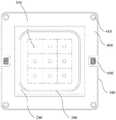
图1为本发明实施例一提供的深紫外发光装置的结构示意图一;FIG. 1 is a schematic structural diagram 1 of a deep ultraviolet light-emitting device according to Embodiment 1 of the present invention;
图2为图1的俯视图;Fig. 2 is the top view of Fig. 1;
图3为本发明实施例一提供的深紫外发光装置的结构示意图二;FIG. 3 is a second schematic structural diagram of the deep ultraviolet light-emitting device according to the first embodiment of the present invention;
图4为本发明实施例二提供的深紫外发光装置的结构示意图;FIG. 4 is a schematic structural diagram of a deep ultraviolet light-emitting device according to Embodiment 2 of the present invention;
图5为本发明实施例三提供的深紫外发光装置的结构示意图。FIG. 5 is a schematic structural diagram of a deep ultraviolet light emitting device according to Embodiment 3 of the present invention.
附图标记说明:Description of reference numbers:
100-基板;100-substrate;
110-第一连接孔;110 - the first connection hole;
120-卡接槽;120-card slot;
130-围坝;130 - dam;
140-凸台;140 - boss;
200-光学透镜;200 - optical lens;
300-密封垫圈;300 - sealing gasket;
400-透光盖;400-translucent cover;
410-第二连接孔;410 - the second connection hole;
420-透光部;420-transparent part;
500-深紫外LED芯片;500-Deep UV LED chip;
600-金属引脚;600 - metal pins;
700-环形螺丝。700-ring screw.
具体实施方式Detailed ways
由于深紫外LED的晶体生长质量较差,外量子效率低于10%,因此光辐射效率很低,而且为了获取较高的光功率,较高的输入功率会导致深紫外LED的发热问题严重。传统的深紫外发光装置中,通常使用导热系数优良的金属材料或陶瓷材料搭配光学透镜,通过胶水粘接构成壳体,将深紫外LED芯片封装在壳体内形成封装元件,多个封装元件二次焊接在基板上,基板再被设置在封闭的保护壳中。传统的深紫外发光装置存在较多缺点:一方面,由于有机胶水键能低,很容易被深紫外光破坏而发生劣化,容易开胶导致光学透镜脱落,且胶水中有机物的挥发还会造成紫外光光衰等,在解决上述问题时,相关技术通常采用低熔点合金材料替代有机胶水,或者以激光石英玻璃实现封装,但这样的方式工艺复杂,金属材料及制作工艺成本较高,激光烧熔或焊接产生的高温还会影响到深紫外LED芯片的性能,可靠性差;另一方面,传统的深紫外发光装置将深紫外LED芯片多次封装,形成了多个空气-透镜界面,由于深紫外发光装置发射出的紫外光在多个界面处会发生全反射和吸收,因此多次封装不利于紫外光的释出,导致紫外光取出效率低。Due to the poor crystal growth quality of deep ultraviolet LEDs, the external quantum efficiency is lower than 10%, so the optical radiation efficiency is very low, and in order to obtain higher optical power, higher input power will lead to serious heating problems in deep ultraviolet LEDs. In traditional deep ultraviolet light-emitting devices, metal materials or ceramic materials with excellent thermal conductivity are usually used together with optical lenses, and the shell is formed by bonding with glue, and the deep ultraviolet LED chips are packaged in the shell to form package components. Soldered on the base plate, the base plate is then placed in a closed protective case. The traditional deep ultraviolet light-emitting device has many disadvantages: on the one hand, due to the low bond energy of organic glue, it is easy to be damaged by deep ultraviolet light and deteriorate, and it is easy to open the glue and cause the optical lens to fall off, and the volatilization of organic matter in the glue will also cause ultraviolet light. When solving the above problems, related technologies usually use low-melting alloy materials to replace organic glue, or use laser quartz glass to achieve packaging, but such methods are complicated in process, high in metal materials and production process costs, and laser melting or The high temperature generated by welding will also affect the performance of the deep ultraviolet LED chip, and the reliability is poor; on the other hand, the traditional deep ultraviolet light emitting device encapsulates the deep ultraviolet LED chip multiple times to form multiple air-lens interfaces. The ultraviolet light emitted by the device will undergo total reflection and absorption at multiple interfaces, so multiple encapsulation is not conducive to the release of ultraviolet light, resulting in low extraction efficiency of ultraviolet light.
针对传统的深紫外发光装置多次封装可靠性差且紫外光取出效率低的缺陷,本发明实施例提供了一种改进的技术方案,在该技术方案中,深紫外发光装置包括基板、光学透镜、密封垫圈、透光盖以及至少一个深紫外LED芯片,深紫外LED芯片焊接在基板上,密封垫圈、光学透镜以及透光盖依次扣合在基板上,形成了容纳深紫外LED芯片的空间,本发明实施例提供的深紫外发光装置整体结构简单,封装严密,且深紫外LED芯片发出的紫外光仅需穿过光学透镜,因此紫外光取出效率高,解决了深紫外LED发光装置结构复杂、紫外光取出效率低的问题。Aiming at the defects of poor reliability of multiple packaging and low ultraviolet light extraction efficiency of the traditional deep ultraviolet light emitting device, the embodiment of the present invention provides an improved technical solution. In the technical solution, the deep ultraviolet light emitting device includes a substrate, an optical lens, a A sealing gasket, a light-transmitting cover and at least one deep-ultraviolet LED chip, the deep-ultraviolet LED chip is welded on the substrate, and the sealing gasket, the optical lens and the light-transmitting cover are sequentially fastened on the substrate, forming a space for accommodating the deep-ultraviolet LED chip. The overall structure of the deep ultraviolet light-emitting device provided by the embodiment of the invention is simple, the packaging is tight, and the ultraviolet light emitted by the deep ultraviolet LED chip only needs to pass through the optical lens, so the ultraviolet light extraction efficiency is high, and the complex structure of the deep ultraviolet LED light-emitting device is solved. The problem of low light extraction efficiency.
为了使本发明实施例的上述目的、特征和优点能够更加明显易懂,下面将结合本发明实施例中的附图,对本发明实施例中的技术方案进行清楚、完整地描述。显然,所描述的实施例仅仅是本发明的一部分实施例,而不是全部的实施例。基于本发明中的实施例,本领域普通技术人员在没有作出创造性劳动的前提下所获得的所有其它实施例,均属于本发明保护的范围。In order to make the above objects, features and advantages of the embodiments of the present invention more clearly and easily understood, the technical solutions in the embodiments of the present invention will be clearly and completely described below with reference to the accompanying drawings in the embodiments of the present invention. Obviously, the described embodiments are only some, but not all, embodiments of the present invention. Based on the embodiments of the present invention, all other embodiments obtained by those of ordinary skill in the art without creative work fall within the protection scope of the present invention.
实施例一Example 1
请参阅图1和图2,图1为本发明实施例一提供的深紫外发光装置的结构示意图;图2为图1的俯视图。Please refer to FIG. 1 and FIG. 2 , FIG. 1 is a schematic structural diagram of a deep ultraviolet light emitting device according to Embodiment 1 of the present invention; FIG. 2 is a top view of FIG. 1 .
本发明实施例一提供的深紫外发光装置包括基板100、光学透镜200、密封垫圈300、透光盖400以及至少一个深紫外LED芯片500,其中,深紫外LED芯片500焊接在基板100的第一表面上,密封垫圈300设置在第一表面上并围绕在深紫外LED芯片500的外围;光学透镜200抵接在密封垫圈300背离基板100的一侧;透光盖400设置在光学透镜200上方并与光学透镜200抵接,透光盖400与基板100连接,透光盖400上设置有透光部420,透光部420对准光学透镜200。The deep ultraviolet light-emitting device provided in the first embodiment of the present invention includes a
具体地,本实施例中的基板100可以是金属基板,也可以是陶瓷基板。基板100可以是圆形基板,也可以是矩形基板。基板100上还设置有焊接层、导电层以及与导电层连接的金属引脚600,金属引脚600用于连接外部供电电路或电源;导电层通常设置为较活泼的金属材料,导电层与焊接层连接;深紫外LED芯片500焊接在上述焊接层上。Specifically, the
进一步地,可以自导电层引出金属引脚600,金属引脚600的正负极可以分别设置在基板100的两侧或同侧,根据设计和使用需求,金属引脚600还可以设置在基板100的第一表面、第二表面或同时设置在第一表面和第二表面。Further, the metal pins 600 can be drawn out from the conductive layer, and the positive and negative electrodes of the metal pins 600 can be respectively arranged on both sides or the same side of the
进一步地,焊接层可以是覆盖在基板100或导电层上的一整层结构,也可以是阵列排布在基板100或导电层上的多个焊点或焊垫结构。Further, the soldering layer may be a whole-layer structure covering the
本实施例中深紫外LED芯片500焊接在基板100的第一表面,需要说明的是,第一表面可以是基板100的顶面或底面的任意一面,在上述实施方式的基础上,第一表面上先设置有焊接层,深紫外LED芯片500焊接在焊接层上。深紫外LED芯片500可以通过金属线键合、共晶焊接、锡膏焊接等方式焊接在基板100的焊接层上,并与焊接层电学连接。In this embodiment, the deep
此外,本发明实施例提供的深紫外发光装置还包括保护芯片,当深紫外LED芯片500为多个时,每个深紫外LED芯片500与一个焊垫电连接,保护芯片可以与对应的深紫外LED芯片500位于同一焊垫上,也可以设置额外的焊垫以焊接保护芯片。保护芯片与深紫外LED芯片500之间的电学关系包含但不限于串联、并联、反串联、反并联等,保护芯片与深紫外LED芯片500其数量可以相等,也可以不相等。本实施例中保护芯片用于提供必要的电学防护环境,用于防止深紫外LED芯片500在不当的使用条件或使用环境下遭受浪涌电流或产生静电击穿等情况。In addition, the deep ultraviolet light-emitting device provided by the embodiment of the present invention further includes a protection chip. When there are multiple deep
当基板100为金属基板时,金属基板的表面预先设置有绝缘层;当基板100为陶瓷基板时,陶瓷基板的表面上设置有导电层和焊接层,导电层上需要覆盖绝缘层。具体地,导电层和焊接层的设置方式有多种,例如:导电层设置在陶瓷基板的第一表面上,焊接层设置在导电层背离陶瓷基板的一侧;再如,焊接层设置在陶瓷基板的第一表面上,导电层设置在陶瓷基板的第二表面上,陶瓷基板上设置有多个导电通孔以连接上述导电层与焊接层。When the
上述绝缘层的材料可以是绝缘油墨,还可以是绝缘氧化物等。绝缘层覆盖在金属基板或导电层上,能够实现绝缘防护,从而防止金属基板或导电层的氧化变色等问题。The material of the above-mentioned insulating layer may be insulating ink, insulating oxide or the like. The insulating layer is covered on the metal substrate or the conductive layer, which can realize insulation protection, thereby preventing problems such as oxidation and discoloration of the metal substrate or the conductive layer.
本实施例中,密封垫圈300设置在基板100的第一表面上,即与深紫外LED芯片500位于基板100的同侧,密封垫圈300可以设置有一个或多个。具体地,深紫外LED芯片500设置有至少一个,密封垫圈300围绕设置在深紫外LED芯片500的外围,例如,当深紫外LED芯片500设置有多个时,多个深紫外LED芯片500均位于密封垫圈300所围成的区域内。In this embodiment, the sealing
密封垫圈300的材料可以是硅橡胶、氢化丁腈橡胶、氟硅橡胶或氯丁橡胶等。密封垫圈300的一侧与基板100接触,另一侧与光学透镜200抵接,在竖直方向上,基板100到光学透镜200之间的距离大于深紫外LED芯片500的厚度。即基板100、密封垫圈300、光学透镜200构成了相对密闭的空腔,将焊接在基板100上的深紫外LED芯片500封装于其中。The material of the sealing
光学透镜200抵接在密封垫圈300背离基板100的一侧,本实施例中光学透镜200的投影应至少覆盖密封垫圈300所围成的区域,光学透镜200的边缘与密封垫圈300的边缘在竖直方向上平齐,或超出密封垫圈300的边缘。优选地,光学透镜200的边缘超出密封垫圈300的边缘,有利于光学透镜200放置的稳定性。The
进一步地,光学透镜200的材料为在紫外光波段具有较高穿透率的材料,例如可以是光学石英玻璃材料;光学透镜200的两个表面可以为平面、球面或具有光学特征结构的其他形状面;光学透镜200的两个表面上还可以涂设有光学增强型薄膜,光学增强型薄膜的材料可以为氟化镁、氟化钙、氧化钛、氧化硅等。光学透镜200的可以设置为一个,也可以设置为包括多个子透镜,具体地,多个子透镜预制在一个透镜载体上,透镜载体抵接在密封垫圈300上,优选地,可以使每个子透镜分别对应一个深紫外LED芯片500。Further, the material of the
透光盖400扣合在光学透镜200上方并与基板100连接,将光学透镜200、密封垫圈300以及基板100上的深紫外LED芯片500封装。如图2所示,基板100为矩形基板,密封垫圈300为方垫圈,相应地,透光盖400也设置为矩形透光盖。本实施例中透光盖400的内侧与光学透镜200抵接,从而防止光学透镜200晃动。The light-transmitting
本实施例中透光盖400设置为筒状,具体地,透光盖400可以为方筒状,也可以为圆筒状。透光盖400上设置有透光部420,透光部420可以为镂空部,也可以为在镂空部上设置有透光玻璃。In this embodiment, the light-transmitting
以透光盖400设置为圆筒状、基板100设置为圆柱形基板100为例进行描述,透光盖400与基板100相连接,连接的方式有多种。Taking the
例如,如图1所示,透光盖400的筒壁具有一定厚度,透光盖400的外径近似等于基板100的直径。透光盖400的一个端面抵接在基板100的第一表面上,另一端沿径向朝内延伸设置有挡边,挡边面向基板100的内侧与光学透镜200背离基板100的一侧面抵接,挡边围成的区域为透光部420。透光盖400与基板100通过依次穿过透光盖400筒壁和基板100的螺栓或螺钉相连接。For example, as shown in FIG. 1 , the cylindrical wall of the light-transmitting
又如,如图3所示,透光盖400的筒壁较薄,透光盖400的内径等于或略大于基板100的直径,基板100能够自透光盖400的一端开口处放入透光盖400的内部,透光盖400的另一端沿径向朝内延伸设置有挡边,挡边面向基板100的内侧与光学透镜200背离基板100的一侧面抵接,挡边围成的区域为透光部420。透光盖400的内壁设置有内螺纹,将设置有外螺纹的环形螺丝700拧入透光盖400,并抵接在基板100的底部,从而将基板100和透光盖400连接,且本实施例中环形螺丝700的中部镂空。For another example, as shown in FIG. 3 , the wall of the light-transmitting
综上所述,本发明实施例一提供的深紫外发光装置将深紫外LED芯片500直接焊接在基板100上,并通过密封垫圈300、光学透镜200以及透光盖400的组合将基板100封装固定,本发明实施例提供的深紫外发光装置结构简单,封装严密,且便于紫外光线的释出,提高了紫外光的取出效率。To sum up, in the deep ultraviolet light emitting device provided in the first embodiment of the present invention, the deep
在一种可能的实现方式中,基板100为陶瓷基板或金属基板。当本实施例中基板100为陶瓷基板时,陶瓷基板的材料具体可以为低温共烧陶瓷、高温共烧陶瓷或者其他导热性较高的金属氮化物陶瓷。当本实施例中基板100为金属基板时,金属基板的材料具体可以为铝、铜或合金。In a possible implementation manner, the
在一种可能的实现方式中,透光盖400的边缘设置有多个第一连接孔110,基板100的边缘对应设置有多个第二连接孔410,透光盖400与基板100通过穿过第一连接孔110和第二连接孔410的螺栓连接。In a possible implementation manner, a plurality of first connection holes 110 are provided on the edge of the light-transmitting
在一种可能的实现方式中,基板100的第一表面设置有用于与密封垫圈300配合的卡接槽120。如图1所示,第一表面上设置有卡接槽120,卡接槽120的形状和尺寸与密封垫圈300相配合,密封垫圈300卡设在上述卡接槽120内,保证了密封垫圈300的稳定性,防止密封垫圈300滑脱。In a possible implementation manner, the first surface of the
在一种可能的实现方式中,基板100的第一表面设置有容纳槽,深紫外LED芯片500焊接在容纳槽内。具体地,当深紫外LED芯片500的数量为多个时,每个深紫外LED芯片500焊接在一个容纳槽内,或者,多个深紫外LED芯片500焊接在一个容纳槽内。容纳槽的开口处以及底部的形状可以为圆形、多边形或者其他任意形状;容纳槽的侧壁可以垂直于基板100的第一表面,也可以与基板100的第一表面之前形成倾角。In a possible implementation manner, the first surface of the
进一步地,容纳槽的内壁上设置有反射涂层,以进一步提高紫外光的取出效率。本实施例中反射涂层可以为金属反射涂层,具体地,反射涂层的材料可以为铝。Further, a reflective coating is provided on the inner wall of the accommodating tank to further improve the extraction efficiency of ultraviolet light. In this embodiment, the reflective coating may be a metal reflective coating, and specifically, the material of the reflective coating may be aluminum.
实施例二Embodiment 2
请参阅图4,图4为本发明实施例二提供的深紫外发光装置的结构示意图。Please refer to FIG. 4 , which is a schematic structural diagram of a deep ultraviolet light emitting device according to Embodiment 2 of the present invention.
本实施例提供的深紫外发光装置包括基板100、光学透镜200、密封垫圈300、透光盖400以及至少一个深紫外LED芯片500,其中,深紫外LED芯片500焊接在基板100的第一表面上,密封垫圈300设置在第一表面上并围绕在深紫外LED芯片500的外围;光学透镜200抵接在密封垫圈300背离基板100的一侧;透光盖400设置在光学透镜200上方并与光学透镜200抵接,透光盖400与基板100连接,透光盖400上设置有透光部420,透光部420对准光学透镜200。The deep ultraviolet light emitting device provided in this embodiment includes a
在上述实施例的基础上,当深紫外LED芯片500的数量为多个时,基板100的第一表面还设置有多个围坝130,每个深紫外LED芯片500焊接在一个围坝130内。具体地,围坝130的数量与深紫外LED芯片500的数量相等。当深紫外LED芯片500设置有多个时,第一表面上设置有多个围坝130,每个围坝130内设置有一个深紫外LED芯片500。On the basis of the above embodiment, when the number of deep ultraviolet LED chips 500 is multiple, the first surface of the
围坝130的顶面开口处以及底部的形状可以为圆形、多边形或者其他任意形状;围坝130在竖直方向上的高度大于或等于位于其内部的深紫外LED芯片500的厚度;围坝130的侧壁可以垂直于基板100的第一表面,也可以与基板100的第一表面之前形成倾角。The shape of the top opening and the bottom of the
进一步地,围坝130的内壁还可以涂设有反射涂层,以进一步提高紫外光的取出效率。Further, the inner wall of the
当深紫外LED芯片500的数量较多时,其分布的面积相对较大,相应的,所需要的光学透镜200面积较大,会造成光学透镜200中部悬空,光学透镜200机械强度较低,当受到挤压、敲击、震动时,可能会导致光学透镜200的破损。本实施例提供的深紫外发光装置在基板100上设置的围坝130为光学透镜200提供了更好的支撑力。此外,围坝130的设置还那个提高深紫外LED芯片500的光取出效率,且围坝130能够将多个深紫外LED芯片500相互隔离,以避免相互之间的光色干扰。When the number of deep ultraviolet LED chips 500 is large, the distribution area is relatively large. Correspondingly, the required area of the
综上所述,本实施例提供的深紫外发光装置通过密封垫圈300、光学透镜200以及透光盖400的组合将基板100封装固定,结构简单;通过在基板100上设置多个围坝130,不仅为光学透镜200提供了支撑力,且进一步提高了深紫外LED芯片500的光取出效率。To sum up, the deep ultraviolet light-emitting device provided in this embodiment encapsulates and fixes the
实施例三Embodiment 3
请参阅图5,图5为本发明实施例三提供的深紫外发光装置的结构示意图。Please refer to FIG. 5 . FIG. 5 is a schematic structural diagram of a deep ultraviolet light emitting device according to Embodiment 3 of the present invention.
本实施例提供的深紫外发光装置包括基板100、光学透镜200、密封垫圈300、透光盖400以及至少一个深紫外LED芯片500,其中,深紫外LED芯片500焊接在基板100的第一表面上,密封垫圈300围绕在深紫外LED芯片500的外围;光学透镜200抵接在密封垫圈300背离基板100的一侧;透光盖400设置在光学透镜200上方并与光学透镜200抵接,透光盖400与基板100连接,透光盖400上设置有透光部420,透光部420对准光学透镜200。The deep ultraviolet light emitting device provided in this embodiment includes a
在上述实施例的基础上,基板100的第一表面沿周向设置有凸台140,凸台140上设置有用于与密封垫圈300配合的卡接槽120。凸台140的材料可以是金属材料,也可以是陶瓷材料,具体地,凸台140的材料与基板100的材料相同。On the basis of the above embodiment, the first surface of the
如图5所示,凸台140在竖直方向上的高度高于焊接在基板100上的深紫外LED芯片500的高度,从而为深紫外LED芯片500提供了足够的空间,防止光学透镜200与深紫外LED芯片500发生干涉和挤压。As shown in FIG. 5 , the height of the
密封垫圈300设置在凸台140的上方,密封垫圈300的底部与凸台140的顶部抵接;光学透镜200面向基板100的一侧抵接在密封垫圈300的顶部。The sealing
在一种可能的实现方式中,透光盖400扣合在凸台140上并与凸台140连接。具体地,透光盖400的一个端面与凸台140的顶面相接触,透光盖400与基板100通过螺栓或螺钉连接,螺栓或螺钉依次穿过透光盖400、凸台140以及位于凸台140下方的基板100部分。In a possible implementation manner, the light-transmitting
综上所述,本实施例提供的深紫外发光装置通过密封垫圈300、光学透镜200以及透光盖400的组合将基板100封装固定,结构简单;通过在基板100上设置凸台140,为深紫外LED芯片500的焊接提供了足够的空间,避免了光学透镜200与深紫外LED芯片500产生干涉。To sum up, the deep ultraviolet light emitting device provided by this embodiment encapsulates and fixes the
本说明书中各实施例或实施方式采用递进的方式描述,每个实施例重点说明的都是与其他实施例的不同之处,各个实施例之间相同相似部分相互参见即可。The embodiments or implementations in this specification are described in a progressive manner, and each embodiment focuses on the differences from other embodiments, and the same and similar parts between the various embodiments may be referred to each other.
在本说明书的描述中,参考术语“一个实施方式”、“一些实施方式”、“示意性实施方式”、“示例”、“具体示例”、或“一些示例”等的描述意指结合实施方式或示例描述的具体特征、结构、材料或者特点包含于本发明的至少一个实施方式或示例中。在本说明书中,对上述术语的示意性表述不一定指的是相同的实施方式或示例。而且,描述的具体特征、结构、材料或者特点可以在任何的一个或多个实施方式或示例中以合适的方式结合。In the description of this specification, reference to the terms "one embodiment," "some embodiments," "exemplary embodiment," "example," "specific example," or "some examples", etc., is meant to incorporate the embodiments A particular feature, structure, material, or characteristic described or exemplified is included in at least one embodiment or example of the present invention. In this specification, schematic representations of the above terms do not necessarily refer to the same embodiment or example. Furthermore, the particular features, structures, materials or characteristics described may be combined in any suitable manner in any one or more embodiments or examples.
最后应说明的是:以上各实施例仅用以说明本发明的技术方案,而非对其限制;尽管参照前述各实施例对本发明进行了详细的说明,本领域的普通技术人员应当理解:其依然可以对前述各实施例所记载的技术方案进行修改,或者对其中部分或者全部技术特征进行等同替换;而这些修改或者替换,并不使相应技术方案的本质脱离本发明各实施例技术方案的范围。Finally, it should be noted that the above embodiments are only used to illustrate the technical solutions of the present invention, but not to limit them; although the present invention has been described in detail with reference to the foregoing embodiments, those of ordinary skill in the art should understand that: The technical solutions described in the foregoing embodiments can still be modified, or some or all of the technical features thereof can be equivalently replaced; and these modifications or replacements do not make the essence of the corresponding technical solutions deviate from the technical solutions of the embodiments of the present invention. scope.
Claims (9)
Priority Applications (1)
| Application Number | Priority Date | Filing Date | Title |
|---|---|---|---|
| CN201911328889.5ACN111029335B (en) | 2019-12-20 | 2019-12-20 | deep ultraviolet light-emitting device |
Applications Claiming Priority (1)
| Application Number | Priority Date | Filing Date | Title |
|---|---|---|---|
| CN201911328889.5ACN111029335B (en) | 2019-12-20 | 2019-12-20 | deep ultraviolet light-emitting device |
Publications (2)
| Publication Number | Publication Date |
|---|---|
| CN111029335A CN111029335A (en) | 2020-04-17 |
| CN111029335Btrue CN111029335B (en) | 2022-04-12 |
Family
ID=70211315
Family Applications (1)
| Application Number | Title | Priority Date | Filing Date |
|---|---|---|---|
| CN201911328889.5AActiveCN111029335B (en) | 2019-12-20 | 2019-12-20 | deep ultraviolet light-emitting device |
Country Status (1)
| Country | Link |
|---|---|
| CN (1) | CN111029335B (en) |
Families Citing this family (3)
| Publication number | Priority date | Publication date | Assignee | Title |
|---|---|---|---|---|
| CN112535745A (en)* | 2020-12-16 | 2021-03-23 | 东莞市翔光光电科技有限公司 | Deep ultraviolet germicidal lamp adopting fluorescent sealant and working state indicating method thereof |
| CN112535746A (en)* | 2020-12-16 | 2021-03-23 | 东莞市翔光光电科技有限公司 | Deep ultraviolet germicidal lamp adopting fluorescent lamp cup and working state indicating method thereof |
| CN112542535A (en)* | 2020-12-16 | 2021-03-23 | 东莞市翔光光电科技有限公司 | Deep ultraviolet germicidal lamp using fluorescent ceramic ring and working state indicating method thereof |
Citations (8)
| Publication number | Priority date | Publication date | Assignee | Title |
|---|---|---|---|---|
| CN102194973A (en)* | 2010-02-02 | 2011-09-21 | 中山大学 | Ultraviolet LED packaging structure and wafer-grade packaging method thereof |
| CN206148467U (en)* | 2016-10-13 | 2017-05-03 | 中山市成源光电科技有限公司 | New COB integrated bracket |
| CN106653984A (en)* | 2017-02-13 | 2017-05-10 | 陶尊伍 | Pouring and packaging type LED anti-explosion light source module and anti-explosion lamp |
| CN206332050U (en)* | 2016-12-30 | 2017-07-14 | 青岛杰生电气有限公司 | A kind of deep-UV light-emitting unit rack and light-emitting device with multi-functional block |
| CN206490092U (en)* | 2017-02-13 | 2017-09-12 | 陶尊伍 | Pouring type LED Anti-explosion light sources module and explosion-proof lamp |
| CN107949922A (en)* | 2015-09-08 | 2018-04-20 | 首尔伟傲世有限公司 | LED Package |
| CN109742212A (en)* | 2018-12-21 | 2019-05-10 | 华中科技大学鄂州工业技术研究院 | A kind of LED packaging structure and packaging method |
| CN109888079A (en)* | 2019-01-22 | 2019-06-14 | 圆融光电科技股份有限公司 | A kind of deep-UV light-emitting diode encapsulation |
Family Cites Families (4)
| Publication number | Priority date | Publication date | Assignee | Title |
|---|---|---|---|---|
| CN203733832U (en)* | 2013-12-25 | 2014-07-23 | 深圳市瑞丰光电子股份有限公司 | Led packaging structure |
| CN106299087B (en)* | 2016-10-21 | 2018-11-13 | 佛山市国星光电股份有限公司 | A kind of deep ultraviolet LED encapsulation structure and its packaging method |
| TWI678816B (en)* | 2017-01-20 | 2019-12-01 | 聯京光電股份有限公司 | Light emitting package base structure |
| CN110197865B (en)* | 2019-05-14 | 2021-02-12 | 湖北深紫科技有限公司 | A liquid encapsulated deep ultraviolet LED package device and preparation method thereof |
- 2019
- 2019-12-20CNCN201911328889.5Apatent/CN111029335B/enactiveActive
Patent Citations (8)
| Publication number | Priority date | Publication date | Assignee | Title |
|---|---|---|---|---|
| CN102194973A (en)* | 2010-02-02 | 2011-09-21 | 中山大学 | Ultraviolet LED packaging structure and wafer-grade packaging method thereof |
| CN107949922A (en)* | 2015-09-08 | 2018-04-20 | 首尔伟傲世有限公司 | LED Package |
| CN206148467U (en)* | 2016-10-13 | 2017-05-03 | 中山市成源光电科技有限公司 | New COB integrated bracket |
| CN206332050U (en)* | 2016-12-30 | 2017-07-14 | 青岛杰生电气有限公司 | A kind of deep-UV light-emitting unit rack and light-emitting device with multi-functional block |
| CN106653984A (en)* | 2017-02-13 | 2017-05-10 | 陶尊伍 | Pouring and packaging type LED anti-explosion light source module and anti-explosion lamp |
| CN206490092U (en)* | 2017-02-13 | 2017-09-12 | 陶尊伍 | Pouring type LED Anti-explosion light sources module and explosion-proof lamp |
| CN109742212A (en)* | 2018-12-21 | 2019-05-10 | 华中科技大学鄂州工业技术研究院 | A kind of LED packaging structure and packaging method |
| CN109888079A (en)* | 2019-01-22 | 2019-06-14 | 圆融光电科技股份有限公司 | A kind of deep-UV light-emitting diode encapsulation |
Also Published As
| Publication number | Publication date |
|---|---|
| CN111029335A (en) | 2020-04-17 |
Similar Documents
| Publication | Publication Date | Title |
|---|---|---|
| TWI656300B (en) | Illuminating device | |
| CN111029335B (en) | deep ultraviolet light-emitting device | |
| US12163630B2 (en) | Lighting apparatus | |
| TWI460890B (en) | Led package structure | |
| US10056358B2 (en) | Light-emitting module | |
| US9857049B2 (en) | LED illumination device | |
| CN108389951B (en) | A kind of deep ultraviolet LED encapsulation structure and preparation method thereof | |
| JP2011238933A (en) | Light emitting device module and illumination system | |
| CN111640846B (en) | Deep UV LED Packaging and Lamps | |
| CN104037302B (en) | LED (light-emitting diode) package assembly | |
| CN101132041A (en) | Encapsulation structure for improving light extraction efficiency of power light-emitting diodes | |
| CN103050582A (en) | Packaging method for light emitting diode with glue wall | |
| CN109509827B (en) | Deep ultraviolet semiconductor light emitting diode device and preparation method thereof | |
| CN104900781B (en) | Light emitting device | |
| US9257620B1 (en) | Package structure of light-emitting diode module and method for manufacturing the same | |
| CN108305927A (en) | A kind of direct insertion deep ultraviolet LED of inorganic encapsulated | |
| CN108321282B (en) | Ultraviolet LED packaging device | |
| CN104282830B (en) | LED Module | |
| CN110323322A (en) | A kind of even smooth LED encapsulation structure of short distance | |
| CN108413264A (en) | A kind of high light-emitting rate ultraviolet LED lighting device | |
| CN103633235A (en) | LED module and manufacturing process thereof | |
| TW201316565A (en) | Packaging method of light emitting diode with glue wall | |
| TW202115345A (en) | This utility model relates to a led package structure and light-emitting device | |
| CN202901966U (en) | Light emitting diode (LED) lamp | |
| CN118156392A (en) | A multi-chip packaging structure for deep ultraviolet LEDs |
Legal Events
| Date | Code | Title | Description |
|---|---|---|---|
| PB01 | Publication | ||
| PB01 | Publication | ||
| SE01 | Entry into force of request for substantive examination | ||
| SE01 | Entry into force of request for substantive examination | ||
| GR01 | Patent grant | ||
| GR01 | Patent grant |