CN110992863B - Electromagnetic interference suppression circuit, driving method thereof, and electronic equipment - Google Patents
Electromagnetic interference suppression circuit, driving method thereof, and electronic equipmentDownload PDFInfo
- Publication number
- CN110992863B CN110992863BCN201911164314.4ACN201911164314ACN110992863BCN 110992863 BCN110992863 BCN 110992863BCN 201911164314 ACN201911164314 ACN 201911164314ACN 110992863 BCN110992863 BCN 110992863B
- Authority
- CN
- China
- Prior art keywords
- gate
- signal
- power supply
- output
- terminal
- Prior art date
- Legal status (The legal status is an assumption and is not a legal conclusion. Google has not performed a legal analysis and makes no representation as to the accuracy of the status listed.)
- Active
Links
Images


Classifications
- H—ELECTRICITY
- H02—GENERATION; CONVERSION OR DISTRIBUTION OF ELECTRIC POWER
- H02M—APPARATUS FOR CONVERSION BETWEEN AC AND AC, BETWEEN AC AND DC, OR BETWEEN DC AND DC, AND FOR USE WITH MAINS OR SIMILAR POWER SUPPLY SYSTEMS; CONVERSION OF DC OR AC INPUT POWER INTO SURGE OUTPUT POWER; CONTROL OR REGULATION THEREOF
- H02M1/00—Details of apparatus for conversion
- H02M1/44—Circuits or arrangements for compensating for electromagnetic interference in converters or inverters
- G—PHYSICS
- G09—EDUCATION; CRYPTOGRAPHY; DISPLAY; ADVERTISING; SEALS
- G09G—ARRANGEMENTS OR CIRCUITS FOR CONTROL OF INDICATING DEVICES USING STATIC MEANS TO PRESENT VARIABLE INFORMATION
- G09G3/00—Control arrangements or circuits, of interest only in connection with visual indicators other than cathode-ray tubes
- G09G3/20—Control arrangements or circuits, of interest only in connection with visual indicators other than cathode-ray tubes for presentation of an assembly of a number of characters, e.g. a page, by composing the assembly by combination of individual elements arranged in a matrix no fixed position being assigned to or needed to be assigned to the individual characters or partial characters
- H—ELECTRICITY
- H03—ELECTRONIC CIRCUITRY
- H03K—PULSE TECHNIQUE
- H03K5/00—Manipulating of pulses not covered by one of the other main groups of this subclass
- H03K5/125—Discriminating pulses
- H03K5/1252—Suppression or limitation of noise or interference
- G—PHYSICS
- G09—EDUCATION; CRYPTOGRAPHY; DISPLAY; ADVERTISING; SEALS
- G09G—ARRANGEMENTS OR CIRCUITS FOR CONTROL OF INDICATING DEVICES USING STATIC MEANS TO PRESENT VARIABLE INFORMATION
- G09G2330/00—Aspects of power supply; Aspects of display protection and defect management
- G09G2330/02—Details of power systems and of start or stop of display operation
- G09G2330/025—Reduction of instantaneous peaks of current
- G—PHYSICS
- G09—EDUCATION; CRYPTOGRAPHY; DISPLAY; ADVERTISING; SEALS
- G09G—ARRANGEMENTS OR CIRCUITS FOR CONTROL OF INDICATING DEVICES USING STATIC MEANS TO PRESENT VARIABLE INFORMATION
- G09G2330/00—Aspects of power supply; Aspects of display protection and defect management
- G09G2330/06—Handling electromagnetic interferences [EMI], covering emitted as well as received electromagnetic radiation
- H—ELECTRICITY
- H03—ELECTRONIC CIRCUITRY
- H03K—PULSE TECHNIQUE
- H03K19/00—Logic circuits, i.e. having at least two inputs acting on one output; Inverting circuits
- H03K19/20—Logic circuits, i.e. having at least two inputs acting on one output; Inverting circuits characterised by logic function, e.g. AND, OR, NOR, NOT circuits
- H03K19/21—EXCLUSIVE-OR circuits, i.e. giving output if input signal exists at only one input; COINCIDENCE circuits, i.e. giving output only if all input signals are identical
- Y—GENERAL TAGGING OF NEW TECHNOLOGICAL DEVELOPMENTS; GENERAL TAGGING OF CROSS-SECTIONAL TECHNOLOGIES SPANNING OVER SEVERAL SECTIONS OF THE IPC; TECHNICAL SUBJECTS COVERED BY FORMER USPC CROSS-REFERENCE ART COLLECTIONS [XRACs] AND DIGESTS
- Y02—TECHNOLOGIES OR APPLICATIONS FOR MITIGATION OR ADAPTATION AGAINST CLIMATE CHANGE
- Y02B—CLIMATE CHANGE MITIGATION TECHNOLOGIES RELATED TO BUILDINGS, e.g. HOUSING, HOUSE APPLIANCES OR RELATED END-USER APPLICATIONS
- Y02B70/00—Technologies for an efficient end-user side electric power management and consumption
- Y02B70/10—Technologies improving the efficiency by using switched-mode power supplies [SMPS], i.e. efficient power electronics conversion e.g. power factor correction or reduction of losses in power supplies or efficient standby modes
Landscapes
- Engineering & Computer Science (AREA)
- Physics & Mathematics (AREA)
- Electromagnetism (AREA)
- Power Engineering (AREA)
- Computer Hardware Design (AREA)
- General Physics & Mathematics (AREA)
- Theoretical Computer Science (AREA)
- Nonlinear Science (AREA)
- Control Of Indicators Other Than Cathode Ray Tubes (AREA)
- Dc-Dc Converters (AREA)
- Electronic Switches (AREA)
Abstract
Description
Translated fromChinese技术领域Technical Field
本公开涉及显示技术领域,特别涉及一种电磁干扰抑制电路及其驱动方法、电子设备。The present disclosure relates to the field of display technology, and in particular to an electromagnetic interference suppression circuit and a driving method thereof, and an electronic device.
背景技术Background Art
随着显示技术的发展,开关电源因其体积小、功耗低和效率高等优点被广泛的应用于各类电子设备中。但是,因开关电源工作频率较高,且在导通和关闭瞬间电压变化率和电流变化率较大等因素的影响,导致开关电源易产生电磁干扰(ElectromagneticInterference,EMI)。With the development of display technology, switching power supplies are widely used in various electronic devices due to their small size, low power consumption and high efficiency. However, due to the high operating frequency of the switching power supply and the large voltage and current change rates at the moment of turn-on and turn-off, the switching power supply is prone to electromagnetic interference (EMI).
目前,可以采用滤波组件(如共模电感和电容)等对开关电源产生的EMI进行滤波,从而达到降低EMI的效果。但是,因滤波组件的体积较大、成本较高,导致采用该方法抑制EMI的成本也较大。At present, filtering components (such as common mode inductors and capacitors) can be used to filter the EMI generated by the switching power supply, thereby achieving the effect of reducing EMI. However, due to the large size and high cost of the filtering components, the cost of suppressing EMI using this method is also high.
发明内容Summary of the invention
本公开实施例提供了一种电磁干扰抑制电路及其驱动方法、电子设备,可以解决相关技术中抑制EMI的成本较较大的问题,所述技术方案如下:The embodiments of the present disclosure provide an electromagnetic interference suppression circuit and a driving method thereof, and an electronic device, which can solve the problem of high cost of suppressing EMI in related technologies. The technical solution is as follows:
一方面,提供了一种电磁干扰抑制电路,所述电路包括:信号发生子电路和频率发生子电路;In one aspect, an electromagnetic interference suppression circuit is provided, the circuit comprising: a signal generation subcircuit and a frequency generation subcircuit;
所述信号发生子电路分别与信号源、时钟信号端和所述频率发生子电路连接,所述信号发生子电路用于响应于所述信号源提供的初始信号和所述时钟信号端提供的时钟信号,向所述频率发生子电路输出多路并行的序列信号,每路序列信号的周期大于周期阈值,且所述并行的序列信号的路数大于数量阈值;The signal generating subcircuit is connected to the signal source, the clock signal terminal and the frequency generating subcircuit respectively, and the signal generating subcircuit is used to output multiple parallel sequence signals to the frequency generating subcircuit in response to the initial signal provided by the signal source and the clock signal provided by the clock signal terminal, wherein the period of each sequence signal is greater than the period threshold, and the number of parallel sequence signals is greater than the number threshold;
所述频率发生子电路还分别与第一电源端和开关电源连接,所述频率发生子电路用于响应于所述多路并行的序列信号和所述第一电源端提供的第一电源信号,向所述开关电源输出频率抖动的驱动信号,所述驱动信号用于驱动所述开关电源工作。The frequency generating sub-circuit is also connected to the first power supply terminal and the switching power supply respectively. The frequency generating sub-circuit is used to output a frequency-jittered driving signal to the switching power supply in response to the multiple parallel sequence signals and the first power supply signal provided by the first power supply terminal. The driving signal is used to drive the switching power supply to operate.
可选的,所述信号发生子电路包括:第一序列发生器和译码器,所述译码器具有多个输入端和多个输出端,且所述译码器的输入端的数量小于所述数量阈值,输出端的数量大于所述数量阈值;Optionally, the signal generating subcircuit includes: a first sequence generator and a decoder, the decoder having a plurality of input terminals and a plurality of output terminals, and the number of the input terminals of the decoder is less than the number threshold, and the number of the output terminals is greater than the number threshold;
所述第一序列发生器分别与所述信号源、所述时钟信号端和所述译码器的多个输入端连接,所述第一序列发生器用于响应于所述初始信号和所述时钟信号,通过所述译码器的多个输入端向所述译码器输出多路并行的初始序列信号,每路初始序列信号的周期大于所述周期阈值;The first sequence generator is connected to the signal source, the clock signal terminal and the multiple input terminals of the decoder respectively, and the first sequence generator is used to respond to the initial signal and the clock signal, and output multiple parallel initial sequence signals to the decoder through the multiple input terminals of the decoder, and the period of each initial sequence signal is greater than the period threshold;
所述译码器的多个输出端与所述频率发生子电路连接,所述译码器用于响应于所述多路并行的初始序列信号,向所述频率发生子电路输出所述多路并行的序列信号。The multiple output terminals of the decoder are connected to the frequency generation sub-circuit, and the decoder is used to output the multiple parallel sequence signals to the frequency generation sub-circuit in response to the multiple parallel initial sequence signals.
可选的,所述第一序列发生器包括:多个D触发器和逻辑门单元;Optionally, the first sequence generator includes: a plurality of D flip-flops and logic gate units;
所述多个D触发器的时钟信号接口均与所述时钟信号端连接,第一个所述D触发器的输入端与所述信号源和所述逻辑门单元的输出端连接,除第一个所述D触发器之外每个所述D触发器的输入端与上一个D触发器的输出端连接,每个所述D触发器的输出端均与所述逻辑门单元的输入端连接;The clock signal interfaces of the plurality of D flip-flops are all connected to the clock signal terminal, the input terminal of the first D flip-flop is connected to the signal source and the output terminal of the logic gate unit, the input terminal of each D flip-flop except the first D flip-flop is connected to the output terminal of the previous D flip-flop, and the output terminal of each D flip-flop is connected to the input terminal of the logic gate unit;
所述逻辑门单元的输出端还与所述译码器的多个输入端连接,所述逻辑门单元用于基于所述多个D触发器的输出端输出的信号,生成所述多路并行的初始序列信号。The output end of the logic gate unit is also connected to multiple input ends of the decoder, and the logic gate unit is used to generate the multi-path parallel initial sequence signals based on the signals output by the output ends of the multiple D flip-flops.
可选的,所述第一序列发生器包括:十个D触发器;所述逻辑门单元包括:七个或非门、四个与非门、一个与门、一个异或门和一个或门;Optionally, the first sequence generator includes: ten D flip-flops; the logic gate unit includes: seven NOR gates, four NAND gates, one AND gate, one XOR gate and one OR gate;
第一个D触发器的输出端和第二个D触发器的输出端与第一个或非门的输入端连接,第三个D触发器至第六个D触发器的输出端与第二个或非门的输入端连接,第七个D触发器至第十个D触发器的输出端与第三个或非门的输入端连接,且第七个D触发器的输出端和第十个D触发器的输出端与所述异或门的输入端连接;The output end of the first D flip-flop and the output end of the second D flip-flop are connected to the input end of the first NOR gate, the output ends of the third to sixth D flip-flops are connected to the input end of the second NOR gate, the output ends of the seventh to tenth D flip-flops are connected to the input end of the third NOR gate, and the output end of the seventh D flip-flop and the output end of the tenth D flip-flop are connected to the input end of the XOR gate;
第一个或非门的输出端、第二个或非门的输出端和第三个或非门的输出端均与所述与门的输入端连接,所述与门的输出端和所述异或门的输出端与所述或门的输入端连接,所述或门的输出端与第一个D触发器的输入端连接;The output end of the first NOR gate, the output end of the second NOR gate and the output end of the third NOR gate are all connected to the input end of the AND gate, the output end of the AND gate and the output end of the XOR gate are connected to the input end of the OR gate, and the output end of the OR gate is connected to the input end of the first D flip-flop;
第一个D触发器的输出端还与第四个或非门的输入端连接,第二个D触发器的输出端还与第五个或非门的输入端连接,第三个D触发器的输出端还与第六个或非门的输入端连接,第四个D触发器的输出端还与第七个或非门的输入端连接,且第四个或非门至第七个或非门的输入端还与初始信号端连接;The output end of the first D flip-flop is also connected to the input end of the fourth NOR gate, the output end of the second D flip-flop is also connected to the input end of the fifth NOR gate, the output end of the third D flip-flop is also connected to the input end of the sixth NOR gate, the output end of the fourth D flip-flop is also connected to the input end of the seventh NOR gate, and the input ends of the fourth NOR gate to the seventh NOR gate are also connected to the initial signal end;
第一个与非门的输入端与所述第四个或非门的输入端和所述译码器的输入端连接,第二个与非门的输入端与所述第五个或非门的输入端和所述译码器的输入端连接,第三个与非门的输入端与所述第六个或非门的输入端和所述译码器的输入端连接,第四个与非门的输入端与所述第七个或非门的输入端和所述译码器的输入端连接。The input end of the first NAND gate is connected to the input end of the fourth NOR gate and the input end of the decoder, the input end of the second NAND gate is connected to the input end of the fifth NOR gate and the input end of the decoder, the input end of the third NAND gate is connected to the input end of the sixth NOR gate and the input end of the decoder, and the input end of the fourth NAND gate is connected to the input end of the seventh NOR gate and the input end of the decoder.
可选的,所述信号发生子电路包括:第二序列发生器,所述第二序列发生器具有输入端和多个输出端,且所述第二序列发生器的输出端的数量大于所述数量阈值;Optionally, the signal generating subcircuit includes: a second sequence generator, the second sequence generator having an input end and a plurality of output ends, and the number of the output ends of the second sequence generator is greater than the number threshold;
所述第二序列发生器的输入端分别与所述信号源和所述时钟信号端连接,所述第二序列发生器的多个输出端与所述频率发生子电路连接,所述多个第二序列发生器用于响应于所述初始信号和所述时钟信号,生成所述多路并行的序列信号,并通过其多个输出端输出至所述频率发生子电路。The input end of the second sequence generator is connected to the signal source and the clock signal end respectively, and the multiple output ends of the second sequence generator are connected to the frequency generation sub-circuit. The multiple second sequence generators are used to respond to the initial signal and the clock signal to generate the multi-channel parallel sequence signals, and output them to the frequency generation sub-circuit through their multiple output ends.
可选的,所述频率发生子电路包括:电流提供单元和频率发生单元;Optionally, the frequency generation subcircuit includes: a current providing unit and a frequency generating unit;
所述电流提供单元分别与所述第一电源端、所述信号发生子电路和所述频率发生单元连接,所述电流提供单元用于响应于所述多路并行的序列信号和所述第一电源信号,向所述频率发生单元输出驱动电流;The current providing unit is connected to the first power supply terminal, the signal generating sub-circuit and the frequency generating unit respectively, and the current providing unit is used to output a driving current to the frequency generating unit in response to the multi-channel parallel sequence signal and the first power supply signal;
所述频率发生单元与所述开关电源连接,所述频率发生单元用于在所述驱动电流的驱动下产生所述频率抖动的驱动信号,并输出至所述开关电源。The frequency generating unit is connected to the switching power supply, and is used for generating the driving signal with the frequency jitter under the driving of the driving current, and outputting the driving signal to the switching power supply.
可选的,所述电流提供单元还与参考电源端连接,所述电流提供单元用于基于所述参考电源端提供的参考电源信号和所述电流提供单元的分压,向所述频率发生单元输出所述驱动电流;所述电流提供单元包括:多个第一开关晶体管、串联的多个第一电阻和电流镜单元;Optionally, the current providing unit is further connected to a reference power supply terminal, and is used to output the driving current to the frequency generating unit based on a reference power supply signal provided by the reference power supply terminal and a voltage division of the current providing unit; the current providing unit includes: a plurality of first switching transistors, a plurality of first resistors connected in series, and a current mirror unit;
所述串联的多个第一电阻的一端与第二电源端连接,另一端与所述电流镜单元连接,所述电流镜单元还分别与所述第一电源端、所述参考电源端和所述频率发生单元连接;One end of the plurality of first resistors connected in series is connected to the second power supply end, and the other end is connected to the current mirror unit, and the current mirror unit is also connected to the first power supply end, the reference power supply end and the frequency generating unit respectively;
每个所述第一开关晶体管的栅极与所述信号发生子电路的一个输出端连接,且各个所述第一开关晶体管的栅极连接的输出端不同;The gate of each of the first switch transistors is connected to an output terminal of the signal generating sub-circuit, and the gates of the first switch transistors are connected to different output terminals;
所述多个第一开关晶体管的第一极均与所述第二电源端连接;The first electrodes of the plurality of first switch transistors are all connected to the second power supply end;
每个所述第一开关晶体管的第二极连接至相邻的两个所述第一电阻之间,且每相邻两个所述第一电阻之间仅连接有一个所述第一开关晶体管的第二极。The second electrode of each first switch transistor is connected between two adjacent first resistors, and only the second electrode of one first switch transistor is connected between every two adjacent first resistors.
可选的,所述电流镜单元包括:第一晶体管、第二晶体管、第三晶体管和比较器;Optionally, the current mirror unit includes: a first transistor, a second transistor, a third transistor and a comparator;
所述比较器的第一输入端与所述参考电源端连接,所述比较器的第二输入端与所述串联的多个第一电阻的另一端连接,所述比较器的输出端与所述第一晶体管的栅极连接;The first input terminal of the comparator is connected to the reference power supply terminal, the second input terminal of the comparator is connected to the other end of the plurality of first resistors connected in series, and the output terminal of the comparator is connected to the gate of the first transistor;
所述第一晶体管的第一极与所述多个第一电阻的另一端连接,所述第一晶体管的第二极与所述第二晶体管的第一极连接;The first electrode of the first transistor is connected to the other end of the plurality of first resistors, and the second electrode of the first transistor is connected to the first electrode of the second transistor;
所述第二晶体管的栅极和所述第三晶体管的栅极连接,所述第二晶体管的第二极和所述第三晶体管的第一极与所述第一电源端连接,所述第三晶体管的第二级与所述频率发生单元连接。The gate of the second transistor is connected to the gate of the third transistor, the second electrode of the second transistor and the first electrode of the third transistor are connected to the first power supply terminal, and the second electrode of the third transistor is connected to the frequency generating unit.
可选的,所述电流提供单元包括:多个第二开关晶体管和串联的多个第二电阻,且所述串联的多个第二电阻的一端与第二电源端连接,另一端与所述第一电源端和所述频率发生单元连接;Optionally, the current providing unit includes: a plurality of second switch transistors and a plurality of second resistors connected in series, wherein one end of the plurality of second resistors connected in series is connected to the second power supply end, and the other end is connected to the first power supply end and the frequency generating unit;
其中,每个所述第二开关晶体管的栅极与所述信号发生子电路的一个输出端连接,且各个所述第二开关晶体管的栅极连接的输出端不同;Wherein, the gate of each second switch transistor is connected to an output terminal of the signal generating sub-circuit, and the output terminals to which the gates of the second switch transistors are connected are different;
所述多个第二开关晶体管的第一极均与所述第二电源端连接;The first electrodes of the plurality of second switch transistors are all connected to the second power supply terminal;
每个所述第二开关晶体管的第二极连接至相邻的两个所述第二电阻之间,且每相邻两个所述第二电阻之间仅连接有一个所述第二开关晶体管的第二极。The second electrode of each second switch transistor is connected between two adjacent second resistors, and only the second electrode of one second switch transistor is connected between every two adjacent second resistors.
另一方面,提供了一种电磁干扰抑制电路的驱动方法,应用于如上述方面所述的电磁干扰抑制电路中,所述方法包括:On the other hand, a driving method of an electromagnetic interference suppression circuit is provided, which is applied to the electromagnetic interference suppression circuit as described in the above aspect, and the method includes:
向信号源提供初始信号,向时钟信号端提供时钟信号,信号发生子电路响应于所述初始信号和所述时钟信号,向频率发生子电路输出多路并行的序列信号,每路所述序列信号的周期大于周期阈值,且所述并行的序列信号的路数大于数量阈值;Providing an initial signal to a signal source and a clock signal to a clock signal terminal, wherein the signal generating subcircuit outputs a plurality of parallel sequence signals to the frequency generating subcircuit in response to the initial signal and the clock signal, wherein the period of each sequence signal is greater than a period threshold, and the number of parallel sequence signals is greater than a quantity threshold;
向第一电源端提供第一电源信号,所述频率发生子电路响应于所述多路并行的序列信号和所述第一电源信号,向开关电源输出频率抖动的驱动信号,所述驱动信号用于驱动所述开关电源工作。A first power supply signal is provided to the first power supply terminal, and the frequency generating sub-circuit outputs a frequency-jittered driving signal to the switching power supply in response to the multiple parallel sequence signals and the first power supply signal, wherein the driving signal is used to drive the switching power supply to operate.
又一方面,提供了一种电子设备,所述电子设备包括:开关电源,以及如上述方面所述的电磁干扰抑制电路,所述电磁干扰抑制电路与所述开关电源连接。On the other hand, an electronic device is provided, comprising: a switching power supply, and the electromagnetic interference suppression circuit as described in the above aspect, wherein the electromagnetic interference suppression circuit is connected to the switching power supply.
本公开实施例提供的技术方案带来的有益效果至少可以包括:The beneficial effects brought by the technical solution provided by the embodiments of the present disclosure may at least include:
综上所述,本公开实施例提供了一种电磁干扰抑制电路及其驱动方法、电子设备,该电磁干扰抑制电路包括信号发生子电路和频率发生子电路。由于该信号发生子电路可以产生周期大于周期阈值,且路数大于数量阈值的多路并行序列信号,该频率发生子电路可以在该多路并行序列信号的控制下,向开关电源输出驱动开关电源工作的频率抖动的驱动信号。因此基于频率抖动技术在节省成本的前提下,有效且可靠的抑制了开关电源产生的电磁干扰。In summary, the embodiments of the present disclosure provide an electromagnetic interference suppression circuit and a driving method thereof, and an electronic device, wherein the electromagnetic interference suppression circuit includes a signal generating subcircuit and a frequency generating subcircuit. Since the signal generating subcircuit can generate a multi-channel parallel sequence signal whose period is greater than the period threshold and the number of channels is greater than the number threshold, the frequency generating subcircuit can output a frequency jittered driving signal to the switching power supply to drive the switching power supply to work under the control of the multi-channel parallel sequence signal. Therefore, based on the frequency jittering technology, the electromagnetic interference generated by the switching power supply is effectively and reliably suppressed under the premise of saving costs.
附图说明BRIEF DESCRIPTION OF THE DRAWINGS
为了更清楚地说明本公开实施例中的技术方案,下面将对实施例描述中所需要使用的附图作简单地介绍,显而易见地,下面描述中的附图仅仅是本公开的一些实施例,对于本领域普通技术人员来讲,在不付出创造性劳动的前提下,还可以根据这些附图获得其他的附图。In order to more clearly illustrate the technical solutions in the embodiments of the present disclosure, the drawings required for use in the description of the embodiments will be briefly introduced below. Obviously, the drawings described below are only some embodiments of the present disclosure. For ordinary technicians in this field, other drawings can be obtained based on these drawings without creative work.
图1是本公开实施例提供的一种基于频率抖动技术抑制EMI的原理示意图;FIG1 is a schematic diagram of a principle of suppressing EMI based on a frequency jittering technology provided by an embodiment of the present disclosure;
图2是本公开实施例提供的一种电磁干扰抑制电路的结构示意图;FIG2 is a schematic diagram of the structure of an electromagnetic interference suppression circuit provided by an embodiment of the present disclosure;
图3是本公开实施例提供的另一种电磁干扰抑制电路的结构示意图;FIG3 is a schematic diagram of the structure of another electromagnetic interference suppression circuit provided by an embodiment of the present disclosure;
图4是本公开实施例提供的一种信号发生子电路的结构示意图;FIG4 is a schematic diagram of the structure of a signal generating subcircuit provided in an embodiment of the present disclosure;
图5是本公开实施例提供的另一种信号发生子电路的结构示意图;FIG5 is a schematic diagram of the structure of another signal generating subcircuit provided in an embodiment of the present disclosure;
图6是本公开实施例提供的又一种电磁干扰抑制电路的结构示意图;FIG6 is a schematic diagram of the structure of another electromagnetic interference suppression circuit provided by an embodiment of the present disclosure;
图7是本公开实施例提供的再一种电磁干扰抑制电路的结构示意图;FIG7 is a schematic diagram of the structure of another electromagnetic interference suppression circuit provided by an embodiment of the present disclosure;
图8是本公开实施例提供的再一种电磁干扰抑制电路的结构示意图;FIG8 is a schematic diagram of the structure of another electromagnetic interference suppression circuit provided by an embodiment of the present disclosure;
图9是本公开实施例提供的再一种电磁干扰抑制电路的结构示意图;FIG9 is a schematic diagram of the structure of another electromagnetic interference suppression circuit provided by an embodiment of the present disclosure;
图10是本公开实施例提供的再一种电磁干扰抑制电路的结构示意图;FIG10 is a schematic diagram of the structure of another electromagnetic interference suppression circuit provided in an embodiment of the present disclosure;
图11是本公开实施例提供的一种电磁干扰抑制电路的驱动方法的流程图;FIG11 is a flow chart of a driving method of an electromagnetic interference suppression circuit provided by an embodiment of the present disclosure;
图12是本公开实施例提供的一种电子设备的结构示意图。FIG. 12 is a schematic diagram of the structure of an electronic device provided in an embodiment of the present disclosure.
具体实施方式DETAILED DESCRIPTION
为了使本公开的目的、技术方案和优点更加清楚,下面将结合附图对本公开实施方式作进一步地详细描述。In order to make the objectives, technical solutions and advantages of the present disclosure more clear, the embodiments of the present disclosure will be further described in detail below with reference to the accompanying drawings.
本公开所有实施例中采用的晶体管均可以为薄膜晶体管或场效应管或其他特性相同的器件,根据在电路中的作用本公开的实施例所采用的晶体管主要为开关晶体管。由于这里采用的开关晶体管的源极、漏极是对称的,所以其源极、漏极是可以互换的。在本公开实施例中,将其中源极称为第一极,漏极称为第二极,或者,将其中漏极称为第一极,源极称为第二极。按附图中的形态规定晶体管的中间端为栅极、信号输入端为源极、信号输出端为漏极。此外,本公开实施例所采用的开关晶体管可以包括P型开关晶体管和N型开关晶体管中的任一种,其中,P型开关晶体管在栅极为低电平时导通,在栅极为高电平时截止,N型开关晶体管在栅极为高电平时导通,在栅极为低电平时截止。此外,本公开各个实施例中的多个信号都对应有第一电位和第二电位,第一电位和第二电位仅代表该信号的电位有2个不同的状态量,不代表全文中第一电位或第二电位具有特定的数值。The transistors used in all embodiments of the present disclosure can be thin film transistors or field effect transistors or other devices with the same characteristics. According to the role in the circuit, the transistors used in the embodiments of the present disclosure are mainly switch transistors. Since the source and drain of the switch transistor used here are symmetrical, the source and drain are interchangeable. In the embodiments of the present disclosure, the source is referred to as the first pole, the drain is referred to as the second pole, or the drain is referred to as the first pole and the source is referred to as the second pole. According to the form in the accompanying drawings, the middle end of the transistor is defined as the gate, the signal input end is the source, and the signal output end is the drain. In addition, the switch transistor used in the embodiments of the present disclosure may include any one of a P-type switch transistor and an N-type switch transistor, wherein the P-type switch transistor is turned on when the gate is at a low level and is turned off when the gate is at a high level, and the N-type switch transistor is turned on when the gate is at a high level and is turned off when the gate is at a low level. In addition, multiple signals in each embodiment of the present disclosure correspond to a first potential and a second potential, and the first potential and the second potential only represent that the potential of the signal has two different state quantities, and do not represent that the first potential or the second potential in the full text has a specific value.
开关电源作为一种高频化电能转换装置被广泛应用于各类电子设备中,且随着科技的不断发展,对开关电源的工作频率要求也越来越高,开关电源的工作频率从几千赫兹发展到几兆赫兹再发展到几百兆赫兹。但正是因开关电源较高的工作频率,以及因开关电源中存在的寄生电容(如电容或电感)导致开关电源在其内部功率开关管导通或关闭瞬间易产生较大电压和电流变化率等因素的影响,导致开关电源易产生较大的涌浪电压和电流,进而导致开关电源易产生EMI。例如,液晶显示面板(Liquid Crystal Display,LCD)中的DC-DC(D irect Current,直流)开关电源产生的EMI为LCD产生EMI的主要来源。As a high-frequency power conversion device, switching power supplies are widely used in various electronic devices. With the continuous development of science and technology, the requirements for the operating frequency of switching power supplies are getting higher and higher. The operating frequency of switching power supplies has developed from several thousand hertz to several megahertz and then to hundreds of megahertz. However, it is precisely because of the high operating frequency of the switching power supply and the parasitic capacitance (such as capacitance or inductance) in the switching power supply that causes the switching power supply to easily produce a large voltage and current change rate when its internal power switch tube is turned on or off, which causes the switching power supply to easily generate a large surge voltage and current, and then causes the switching power supply to easily generate EMI. For example, the EMI generated by the DC-DC (Direct Current) switching power supply in the liquid crystal display panel (Liquid Crystal Display, LCD) is the main source of EMI generated by the LCD.
由于电子设备中开关电源产生的EMI可能会干扰位于该电子设备周围的其他电子设备的正常工作,导致其他电子设备性能下降。因此抑制开关电源产生的EMI在开关电源的设计中越发重要。例如,对于车载电子设备,若不能有效抑制其产生的EMI,可能会影响生命安全,因此为了有效避免车载电子设备之间因EMI而产生互相干扰的问题,确保车载电子设备的使用安全性,对抑制车载电子设备的开关电源产生的EMI提出的了较高的要求。Since the EMI generated by the switching power supply in an electronic device may interfere with the normal operation of other electronic devices located around the electronic device, causing the performance of other electronic devices to deteriorate, it is increasingly important to suppress the EMI generated by the switching power supply in the design of the switching power supply. For example, for vehicle-mounted electronic devices, if the EMI generated by them cannot be effectively suppressed, it may affect life safety. Therefore, in order to effectively avoid the problem of mutual interference between vehicle-mounted electronic devices due to EMI and ensure the safety of vehicle-mounted electronic devices, higher requirements are put forward for suppressing the EMI generated by the switching power supply of vehicle-mounted electronic devices.
相关技术中,可以采用共模电感和电容等有源器件对EMI进行滤波,从而达到降低EMI的效果,但该EMI抑制方法受共模电感和电容体积较大和成本较高等因素的制约,不利于量产。或,可以采用变压器来抑制EMI,但因变压器的绕制难度和绝缘难度均较大,导致抑制EMI的可靠性较差。或,还可以通过设计抑制EMI的印刷电路板(Printed Circuit Board,PCB)来抑制EMI,但因PCB的设计需要丰富的经验,设计和制造难度较大,导致抑制EMI灵活性较差。In the related art, active devices such as common-mode inductors and capacitors can be used to filter EMI, thereby achieving the effect of reducing EMI, but this EMI suppression method is restricted by factors such as the large volume and high cost of common-mode inductors and capacitors, which is not conducive to mass production. Alternatively, a transformer can be used to suppress EMI, but the winding and insulation difficulties of the transformer are relatively large, resulting in poor reliability in suppressing EMI. Alternatively, EMI can also be suppressed by designing a printed circuit board (PCB) that suppresses EMI, but the design of the PCB requires rich experience and is difficult to design and manufacture, resulting in poor flexibility in suppressing EMI.
本公开实施例提供了一种电磁干扰抑制电路,该电磁干扰抑制电路基于频率抖动技术在节省体积减小成本的前提下,有效可靠的抑制了开关电源产生的EMI,且不会对开关电源的工作频率带来其他负面影响,也不会给开关电源的制造带来任何不便。其中,频率抖动技术是指:在总频谱能量不变的前提下,将各次谐波的频带展宽,使得各次谐波的峰值能量得以降低,进而降低EMI。The disclosed embodiment provides an electromagnetic interference suppression circuit, which effectively and reliably suppresses the EMI generated by a switching power supply based on the frequency jitter technology, while saving volume and reducing costs, and does not bring other negative effects on the operating frequency of the switching power supply, nor does it bring any inconvenience to the manufacture of the switching power supply. Among them, the frequency jitter technology refers to: under the premise that the total spectrum energy remains unchanged, the frequency band of each harmonic is widened, so that the peak energy of each harmonic is reduced, thereby reducing EMI.
图1是本公开实施例提供的一种一种基于频率抖动技术抑制EMI的原理示意图。如图1所示,让水龙头的水(可以称为总频谱能量)从一个小孔以固定频率喷洒至花朵上,和让水龙头的水分散能量后从多个小孔分别以不同频率喷洒至花朵上对花朵带来的压力是不同的。结合图1,对比两种情况可以看出,让水龙头的水分散后从多个小孔分别喷出,水的整体喷出力度(相当于EMI)会变小很多,且分散的越多越开,能量分散的效果即会越好。因此,通过调整开关电源的工作频率,使开关电源在抖动的频率而不是固定频率下工作,可以有效降低开关电源产生的EMI。并且,分散周期越大,相同频率的能量出现的几率越低,分散位数越大,频率抖动更加精细。FIG1 is a schematic diagram of the principle of suppressing EMI based on frequency jitter technology provided by an embodiment of the present disclosure. As shown in FIG1 , the pressure on the flowers caused by allowing the water from the faucet (which can be called the total spectrum energy) to be sprayed from a small hole at a fixed frequency and allowing the water from the faucet to disperse the energy and then spray it from multiple small holes at different frequencies is different. In conjunction with FIG1 , by comparing the two situations, it can be seen that when the water from the faucet is dispersed and sprayed from multiple small holes, the overall spraying force of the water (equivalent to EMI) will become much smaller, and the more and more dispersed, the better the effect of energy dispersion will be. Therefore, by adjusting the operating frequency of the switching power supply so that the switching power supply operates at a jittering frequency instead of a fixed frequency, the EMI generated by the switching power supply can be effectively reduced. Moreover, the larger the dispersion period, the lower the probability of the energy of the same frequency appearing, the larger the number of dispersed bits, and the finer the frequency jitter.
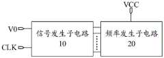
图2是本公开实施例提供的一种电磁干扰抑制电路的结构示意图。如图2所示,该电路可以包括:信号发生子电路10和频率发生子电路20。Fig. 2 is a schematic diagram of the structure of an electromagnetic interference suppression circuit provided by an embodiment of the present disclosure. As shown in Fig. 2 , the circuit may include: a
该信号发生子电路10分别与信号源V0、时钟信号端CLK和频率发生子电路20连接,该信号发生子电路10可以响应于信号源V0提供的初始信号和时钟信号端CLK提供的时钟信号,向频率发生子电路20输出多路并行的序列信号。The
例如,参考图2,该信号发生子电路10通过多个输出端与频率发生子电路20连接,相应的,该信号发生子电路10即可以通过该多个输出端向频率发生子电路20输出多路并行的序列信号。其中,每路序列信号的周期可以大于周期阈值,且并行的序列信号的路数可以大于数量阈值。可选的,该周期阈值和数量阈值可以是预先设定的固定值。For example, referring to FIG2 , the
该频率发生子电路20还可以分别与第一电源端VCC和开关电源(图2未示出)连接。该频率发生子电路20可以响应于多路并行的序列信号和第一电源端VCC提供的第一电源信号,向开关电源输出频率抖动的驱动信号,且该驱动信号可以用于驱动开关电源工作。The
综上所述,本公开实施例提供了一种电磁干扰抑制电路,该电磁干扰抑制电路包括信号发生子电路和频率发生子电路。由于该信号发生子电路可以产生周期大于周期阈值,且路数大于数量阈值的多路并行序列信号,该频率发生子电路可以在该多路并行序列信号的控制下,向开关电源输出驱动开关电源工作的频率抖动的驱动信号。因此基于频率抖动技术在节省成本的前提下,有效且可靠的抑制了开关电源产生的电磁干扰。In summary, the embodiment of the present disclosure provides an electromagnetic interference suppression circuit, which includes a signal generation subcircuit and a frequency generation subcircuit. Since the signal generation subcircuit can generate a multi-channel parallel sequence signal with a period greater than a period threshold and a number of channels greater than a number threshold, the frequency generation subcircuit can output a frequency jittered driving signal to the switching power supply to drive the switching power supply to work under the control of the multi-channel parallel sequence signal. Therefore, based on the frequency jitter technology, the electromagnetic interference generated by the switching power supply is effectively and reliably suppressed under the premise of saving costs.
作为一种可选的实现方式,图3是本公开实施例提供的另一种电磁干扰抑制电路的结构示意图。如图3所示,该信号发生子电路10可以包括:第一序列发生器101和译码器102。该译码器102可以具有多个输入端和多个输出端,且该译码器102的输入端的数量小于数量阈值,输出端的数量大于数量阈值。As an optional implementation, FIG3 is a schematic diagram of the structure of another electromagnetic interference suppression circuit provided by an embodiment of the present disclosure. As shown in FIG3, the
该第一序列发生器101可以分别与信号源V0、时钟信号端CLK和译码器102的多个输入端连接,该第一序列发生器101可以响应于信号源V0提供的初始信号和、时钟信号端CLK提供的时钟信号,通过译码器102的多个输入端向译码器102输出多路并行的初始序列信号。其中,每路初始序列信号的周期可以大于周期阈值。The
该译码器102的多个输出端可以与频率发生子电路20连接。该译码器102可以响应于多路并行的初始序列信号,向频率发生子电路20输出多路并行的序列信号。The multiple output terminals of the
示例的,假设周期阈值为1020,数量阈值为10,该第一序列发生器101生成了4路初始序列信号,且每路序列信号的周期为1024。则可以设置4-15译码器102,即该译码器102即共包括4个输入端和15个输出端。该4-15译码器102可以不改变每路序列信号的周期的前提下,将该4路初始序列信号译码为周期大于周期阈值,且路数大于数量阈值的15路并行的序列信号。可选的,每路序列信号可以以二进制数值0或1的形式表示,0可以代表有效电位,相应的,1即可以代表无效电位。同理,若0代表无效电位,则1即可以代表有效电位。For example, assuming that the period threshold is 1020 and the quantity threshold is 10, the
通过设置第一序列发生器101先产生路数较少,且周期大于周期阈值的多路并行的初始序列信号,再设置译码器102基于初始序列信号,产生周期不变,且路数大于数量阈值即路数较多的多路并行序列信号,可以在实现对EMI的有效抑制的前提下,充分利用译码器不改变周期仅改变路数的原理,实现对EMI的精确抑制。并且,因译码器属于现有的电路结构,因此成本较低,电路制造较为简单,有利于量产。By setting the
图4是本公开实施例提供的一种信号发生子电路的结构示意图。如图4所示,该第一序列发生器101可以包括:多个D触发器(图4示出了n个D触发器)和逻辑门单元1010。FIG4 is a schematic diagram of a signal generation subcircuit provided by an embodiment of the present disclosure. As shown in FIG4 , the
该多个D触发器的时钟信号接口CLK0可以均与同一个时钟信号端CLK连接,第一个D触发器的输入端D可以与信号源V0和逻辑门单元1010的输出端连接(图中未示出),除第一个D触发器之外每个D触发器的输入端D可以与上一个D触发器的输出端O连接,每个D触发器的输出端O可以均与逻辑门单元1010的输入端连接。The clock signal interfaces CLK0 of the multiple D flip-flops can all be connected to the same clock signal terminal CLK, the input terminal D of the first D flip-flop can be connected to the signal source V0 and the output terminal of the logic gate unit 1010 (not shown in the figure), and the input terminal D of each D flip-flop except the first D flip-flop can be connected to the output terminal O of the previous D flip-flop, and the output terminal O of each D flip-flop can be connected to the input terminal of the
逻辑门单元1010输出端还与译码器102的多个输入端连接,逻辑门单元1010可以基于多个D触发器的输出端输出的信号生成多路并行的初始序列信号。The output end of the
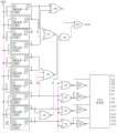
图5是本公实施例提供的另一种信号发生子电路的结构示意图。如图5所示,该第一序列发生器101可以包括:十个D触发器。该逻辑门单元1010可以包括:七个或非门N1、四个与非门N2、一个与门N3、一个异或门N4和一个或门N5。Fig. 5 is a schematic diagram of the structure of another signal generating sub-circuit provided by the present embodiment. As shown in Fig. 5, the
其中,第一个D触发器的输出端O和第二个D触发器的输出端O可以与第一个或非门N1的输入端连接,第三个D触发器至第六个D触发器的输出端O可以与第二个或非门N1的输入端连接,第七个D触发器至第十个D触发器的输出端O可以与第三个或非门N1的输入端连接,且第七个D触发器的输出端O和第十个D触发器的输出端O可以与异或门N4的输入端连接。Among them, the output terminal O of the first D flip-flop and the output terminal O of the second D flip-flop can be connected to the input terminal of the first NOR gate N1, the output terminal O of the third D flip-flop to the sixth D flip-flop can be connected to the input terminal of the second NOR gate N1, the output terminal O of the seventh D flip-flop to the tenth D flip-flop can be connected to the input terminal of the third NOR gate N1, and the output terminal O of the seventh D flip-flop and the output terminal O of the tenth D flip-flop can be connected to the input terminal of the XOR gate N4.
第一个或非门N1的输出端、第二个或非门N1的输出端和第三个或非门N1的输出端可以均与与门N3的输入端连接,与门N3的输出端和异或门N4的输出端可以与或门N5的输入端连接,或门N5的输出端可以与第一个D触发器的输入端D连接。且该第一个D触发器的输入端D还可以与信号源V0连接。The output end of the first NOR gate N1, the output end of the second NOR gate N1 and the output end of the third NOR gate N1 can all be connected to the input end of the AND gate N3, the output end of the AND gate N3 and the output end of the XOR gate N4 can be connected to the input end of the OR gate N5, and the output end of the OR gate N5 can be connected to the input end D of the first D flip-flop. And the input end D of the first D flip-flop can also be connected to the signal source V0.
第一个D触发器的输出端O还可以与第四个或非门N1的输入端连接,第二个D触发器的输出端O还可以与第五个或非门N1的输入端连接,第三个D触发器的输出端O还可以与第六个或非门N1的输入端连接,第四个D触发器的输出端O还可以与第七个或非门N1的输入端连接,且第四个或非门N1至第七个或非门N1的输入端还与初始信号端(图中未示出)连接。The output terminal O of the first D flip-flop can also be connected to the input terminal of the fourth NOR gate N1, the output terminal O of the second D flip-flop can also be connected to the input terminal of the fifth NOR gate N1, the output terminal O of the third D flip-flop can also be connected to the input terminal of the sixth NOR gate N1, the output terminal O of the fourth D flip-flop can also be connected to the input terminal of the seventh NOR gate N1, and the input terminals of the fourth NOR gate N1 to the seventh NOR gate N1 are also connected to the initial signal terminal (not shown in the figure).
第一个与非门N2的输入端与第四个或非门N1的输入端可以与译码器102的输入端连接,第二个与非门N2的输入端与第五个或非门N1的输入端和译码器102的输入端连接,第三个与非门N2的输入端与第六个或非门N1的输入端和译码器102的输入端连接,第四个与非门N2的输入端与第七个或非门N1的输入端和译码器102的输入端连接。The input end of the first NAND gate N2 and the input end of the fourth NOR gate N1 can be connected to the input end of the
相应的,参考图5,该译码器102即可以具有4个输入端,且图5以该译码器具有15个输出端Y1至Y15为例进行说明。对于图5示出的第一序列发生器,与门N5的输出端输出的信号Fout可以满足下述公式:Correspondingly, referring to FIG5 , the
Fout=(Q1+Q2)'(Q3+Q4+Q5+Q6)'(Q7+Q8+Q9+Q10)'+(Q10⊕Q7)';Fout=(Q1+Q2)'(Q3+Q4+Q5+Q6)'(Q7+Q8+Q9+Q10)'+(Q10⊕Q7)';
其中,(Q1+Q2)'是指D触发器(1)和D触发器(2)的输出经第一个或非门N1输出的值,(Q3+Q4+Q5+Q6)'是指D触发器(3)至D触发器(6)的输出经第二个或非门N1输出的值,(Q7+Q8+Q9+Q10)'是指D触发器(7)至D触发器(10)的输出经第三个或非门N1输出的值,(Q10⊕Q7)'是指D触发器(7)和D触发器(10)的输出经异或门N4输出的值。(Q1+Q2)'(Q3+Q4+Q5+Q6)'(Q7+Q8+Q9+Q10)'是指第一个或非门N1输出的值、第二个或非门N1输出的值和第三个或非门N1输出的值经与门N3输出的值。Fout是指与门N3输出的值和异或门N4输出的值经与门N5输出的值。Among them, (Q1+Q2)' refers to the value of the output of D flip-flop (1) and D flip-flop (2) outputted through the first NOR gate N1, (Q3+Q4+Q5+Q6)' refers to the value of the output of D flip-flop (3) to D flip-flop (6) outputted through the second NOR gate N1, (Q7+Q8+Q9+Q10)' refers to the value of the output of D flip-flop (7) to D flip-flop (10) outputted through the third NOR gate N1, (Q10⊕Q7)' refers to the value of the output of D flip-flop (7) and D flip-flop (10) outputted through the XOR gate N4. (Q1+Q2)'(Q3+Q4+Q5+Q6)'(Q7+Q8+Q9+Q10)' refers to the value of the output of the first NOR gate N1, the value of the output of the second NOR gate N1 and the value of the output of the third NOR gate N1 outputted through the AND gate N3. Fout refers to the value of the output of the AND gate N3 and the value of the XOR gate N4 outputted through the AND gate N5.
在本公开实施例中,该Fout可以作为D触发器(1)的输入,最终该第一序列发生器101可以产生周期为210=1024的多路并行的初始序列信号。并且,由于使用了与门N3(在代数运算中代表乘法),使得输出结果为非线性函数。进而,保证了第一序列发生器101能够自启动且不会陷入死循环(即无效状态)。In the disclosed embodiment, the Fout can be used as the input of the D flip-flop (1), and finally the
结合图5,假设第一序列发生器101的输出的4路并行的初始序列信号分别为A、B、C和D,则4-15译码器的15个输出端Y1至Y15输出的信号即可以满足下述公式:5 , assuming that the 4 parallel initial sequence signals output by the

其中,
作为另一种可选的实现方式,图6是本公实施例提供的再一种信号发生子电路的结构示意图。如图6所示,该信号发生子电路10可以包括:第二序列发生器103,第二序列发生器103具有输入端和多个输出端,且第二序列发生器103的输出端的数量大于数量阈值。As another optional implementation, Fig. 6 is a schematic diagram of the structure of another signal generating subcircuit provided by the present embodiment. As shown in Fig. 6, the
该第二序列发生器103的输入端分别与信号源V0和时钟信号端CLK连接,该第二序列发生器103的多个输出端可以直接与频率发生子电路20连接,该多个第二序列发生器103可以响应于初始信号和时钟信号生成多路并行的序列信号,并通过其多个输出端输出至频率发生子电路20。The input end of the
图7是本公开实施例提供的又一种电磁干扰抑制电路的结构示意图。如图7所示,该频率发生子电路20可以包括:电流提供单元201和频率发生单元202。Fig. 7 is a schematic diagram of the structure of another electromagnetic interference suppression circuit provided by an embodiment of the present disclosure. As shown in Fig. 7 , the
该电流提供单元201可以分别与第一电源端VCC、信号发生子电路10和频率发生单元202连接。该电流提供单元201可以响应于多路并行的序列信号和第一电源信号,向频率发生单元202输出驱动电流。The
该频率发生单元202可以与开关电源(图中未示出)连接。该频率发生单元202可以在驱动电流的驱动下产生驱动信号,并输出至开关电源。The
作为一种可选的实现方式,图8是本公开实施例提供的又一种电磁干扰抑制电路的结构示意图。如图8所示,该电流提供单元201还可以与参考电源端Vref连接。该电流提供单元201可以基于参考电源端Vref提供的参考电源信号和电流提供单元201的分压,向频率发生单元202输出驱动电流。As an optional implementation, FIG8 is a schematic diagram of the structure of another electromagnetic interference suppression circuit provided by an embodiment of the present disclosure. As shown in FIG8, the current providing
其中,该参考电源信号可以为根据频率发生单元202的频率调节范围预先设置的电源信号。该电流提供单元201可以在分压大于参考电源信号的电压时,停止输出驱动电流,即停止工作。The reference power signal may be a power signal preset according to the frequency adjustment range of the
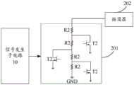
图9是本公开实施例提供的又一种电磁干扰抑制电路的结构示意图。如图9所示,该电流提供单元201可以包括:多个第一开关晶体管T1、串联的多个第一电阻R1和电流镜单元2011。Fig. 9 is a schematic diagram of the structure of another electromagnetic interference suppression circuit provided by an embodiment of the present disclosure. As shown in Fig. 9 , the current providing
参考图9,串联的多个第一电阻R1的一端可以与第二电源端GND连接,另一端可以与电流镜单元2011连接,电流镜单元2011还可以分别与第一电源端VCC、参考电源端Vref和频率发生单元202连接。9 , one end of the plurality of first resistors R1 connected in series may be connected to the second power supply terminal GND, and the other end may be connected to the
每个第一开关晶体管T1的栅极可以与信号发生子电路10的一个输出端连接,且各个第一开关晶体管T1的栅极连接的输出端不同。相应的,各个开关晶体管T1即可以响应于信号发生子电路10输入至其栅极的序列信号的电位开启或关断,开启的开关晶体管T1的数量不同,则会导致接入的第一电阻R1的数量不同,进而即会影响输出至频率发生单元202的驱动电流的大小。The gate of each first switch transistor T1 can be connected to an output terminal of the
多个第一开关晶体管T1的第一极可以均与第二电源端GND连接。The first electrodes of the plurality of first switch transistors T1 may all be connected to the second power supply terminal GND.
每个第一开关晶体管T1的第二极可以连接至相邻的两个第一电阻R1之间,且每相邻两个第一电阻R1之间可以仅连接有一个第一开关晶体管T1的第二极。The second electrode of each first switch transistor T1 may be connected between two adjacent first resistors R1 , and only the second electrode of one first switch transistor T1 may be connected between every two adjacent first resistors R1 .
参考图9,该电流镜单元2011可以包括:第一晶体管M1、第二晶体管M2、第三晶体管M3和比较器A1。9 , the
其中,比较器A1的第一输入端(+)可以与参考电源端Vref连接,比较器A1的第二输入端(-)可以与串联的多个第一电阻R1的另一端连接,比较器A1的输出端可以与第一晶体管M1的栅极连接。Among them, the first input terminal (+) of comparator A1 can be connected to the reference power supply terminal Vref, the second input terminal (-) of comparator A1 can be connected to the other end of multiple first resistors R1 connected in series, and the output terminal of comparator A1 can be connected to the gate of the first transistor M1.
第一晶体管M1的第一极可以与多个第一电阻R1的另一端连接,第一晶体管M1的第二极可以与第二晶体管M2的第一极连接。A first electrode of the first transistor M1 may be connected to the other end of the plurality of first resistors R1 , and a second electrode of the first transistor M1 may be connected to a first electrode of the second transistor M2 .
第二晶体管M2的栅极可以与第三晶体管M3的栅极连接,第二晶体管M2的第二极和第三晶体管M3的第一极可以与第一电源端VCC连接,第三晶体管M3的第二级可以与频率发生单元202连接。The gate of the second transistor M2 can be connected to the gate of the third transistor M3 , the second electrode of the second transistor M2 and the first electrode of the third transistor M3 can be connected to the first power supply terminal VCC, and the second electrode of the third transistor M3 can be connected to the
示例的,结合图5和图9,假设共包括15个第一开关晶体管T1,该15个第一开关晶体管T1的栅极可以分别与译码器的15个输出端Y1至Y15连接。该15个输出端Y1至Y15输出的序列信号的电位影响了该15个第一开关晶体管T1的开启和关断数量。该15个第一开关晶体管T1的开启和关断数量影响了接入的第一电阻R1的数量,相应的,即影响了输出至频率发生单元202的驱动电流的大小。该频率发生单元202可以基于该驱动电流向开关电源输出频率抖动的驱动信号(即工作频率)。需要说明的是,频率发生单元202和开关电源之间还可以连接有分频器和放大器等处理组件。For example, in combination with FIG. 5 and FIG. 9, it is assumed that a total of 15 first switch transistors T1 are included, and the gates of the 15 first switch transistors T1 can be respectively connected to the 15 output terminals Y1 to Y15 of the decoder. The potential of the sequence signal output by the 15 output terminals Y1 to Y15 affects the number of on and off of the 15 first switch transistors T1. The number of on and off of the 15 first switch transistors T1 affects the number of connected first resistors R1, and accordingly, affects the size of the drive current output to the
作为另一种可选的实现方式,图10是本公开实施例提供的又一种电磁干扰抑制电路的结构示意图。如图10所示,该电流提供单元201可以包括:多个第二开关晶体管T2和串联的多个第二电阻R2,且串联的多个第二电阻R2的一端可以与第二电源端GND连接,另一端可以与第一电源端VCC和频率发生单元202连接。As another optional implementation, FIG10 is a schematic diagram of the structure of another electromagnetic interference suppression circuit provided by an embodiment of the present disclosure. As shown in FIG10, the current providing
其中,每个第二开关晶体管T2的栅极可以与信号发生子电路10的一个输出端连接,且各个第二开关晶体管T2的栅极连接的输出端可以不同。The gate of each second switch transistor T2 may be connected to an output terminal of the
多个第二开关晶体管T2的第一极可以均与第二电源端GND连接。The first electrodes of the plurality of second switch transistors T2 may all be connected to the second power supply terminal GND.
每个第二开关晶体管T2的第二极可以连接至相邻的两个第二电阻R2之间,且每相邻两个第二电阻R2之间仅连接有一个第二开关晶体管T2的第二极。The second electrode of each second switch transistor T2 may be connected between two adjacent second resistors R2 , and only the second electrode of one second switch transistor T2 is connected between every two adjacent second resistors R2 .
对于图10所示的电磁干扰抑制电路,其工作原理可以参考上述图9所示的电路结构的工作原理,在此不再赘述。并且,结合图9和图10可以看出,该频率发生单元202可以包括:振荡器。For the electromagnetic interference suppression circuit shown in Fig. 10, its working principle can refer to the working principle of the circuit structure shown in Fig. 9, which will not be described in detail. In addition, it can be seen from Fig. 9 and Fig. 10 that the
需要说明的是,并行的序列信号的路数与电流提供单元201包括的开关晶体管的数量可以相同。通过生成数量相同的多路并行序列信号,可以进一步提高对开关晶体管的控制精度,进而可以提高对EMI进行抑制的精度和效率。It should be noted that the number of parallel sequence signals may be the same as the number of switch transistors included in the current providing
综上所述,本公开实施例提供了一种电磁干扰抑制电路,该电磁干扰抑制电路包括信号发生子电路和频率发生子电路。由于该信号发生子电路可以产生周期大于周期阈值,且路数大于数量阈值的多路并行序列信号,该频率发生子电路可以在该多路并行序列信号的控制下,向开关电源输出驱动开关电源工作的频率抖动的驱动信号。因此基于频率抖动技术在节省成本的前提下,有效且可靠的抑制了开关电源产生的电磁干扰。In summary, the embodiment of the present disclosure provides an electromagnetic interference suppression circuit, which includes a signal generation subcircuit and a frequency generation subcircuit. Since the signal generation subcircuit can generate a multi-channel parallel sequence signal with a period greater than a period threshold and a number of channels greater than a number threshold, the frequency generation subcircuit can output a frequency jittered driving signal to the switching power supply to drive the switching power supply to work under the control of the multi-channel parallel sequence signal. Therefore, based on the frequency jitter technology, the electromagnetic interference generated by the switching power supply is effectively and reliably suppressed under the premise of saving costs.
图11是本公开实施例提供的一种电磁干扰抑制电路的驱动方法流程图,该方法可以应用于如图2至图10任一所示的电磁干扰抑制电路中。如图10所示,该方法可以包括:FIG11 is a flow chart of a driving method of an electromagnetic interference suppression circuit provided by an embodiment of the present disclosure, and the method can be applied to an electromagnetic interference suppression circuit as shown in any one of FIG2 to FIG10. As shown in FIG10, the method may include:
步骤1101、向信号源提供初始信号,向时钟信号端提供时钟信号,信号发生子电路响应于该初始信号和该时钟信号,向频率发生子电路输出多路并行的序列信号。Step 1101: Provide an initial signal to a signal source, provide a clock signal to a clock signal terminal, and the signal generation subcircuit outputs multiple parallel sequence signals to the frequency generation subcircuit in response to the initial signal and the clock signal.
在本公开实施例中,每路序列信号的周期大于周期阈值,且并行的序列信号的路数大于数量阈值。In the embodiment of the present disclosure, the period of each sequence signal is greater than a period threshold, and the number of parallel sequence signals is greater than a number threshold.
步骤1102、向第一电源端提供第一电源信号,频率发生子电路响应于多路并行的序列信号和第一电源信号,向开关电源输出频率抖动的驱动信号。Step 1102: Provide a first power supply signal to a first power supply terminal, and the frequency generating sub-circuit outputs a frequency-dithered driving signal to a switching power supply in response to the multiple parallel sequence signals and the first power supply signal.
其中,该驱动信号用于驱动开关电源工作。The driving signal is used to drive the switching power supply to operate.
综上所述,本公开实施例提供了一种电磁干扰抑制电路的驱动方法,由于信号发生子电路可以产生周期大于周期阈值,且路数大于数量阈值的多路并行序列信号,该频率发生子电路可以在该多路并行序列信号的控制下,向开关电源输出驱动开关电源工作的频率抖动的驱动信号。因此基于频率抖动技术在节省成本的前提下,有效且可靠的抑制了开关电源产生的电磁干扰。In summary, the embodiment of the present disclosure provides a driving method for an electromagnetic interference suppression circuit. Since the signal generation subcircuit can generate a multi-channel parallel sequence signal with a period greater than a period threshold and a number of channels greater than a number threshold, the frequency generation subcircuit can output a frequency-dithered driving signal to the switching power supply to drive the switching power supply to work under the control of the multi-channel parallel sequence signal. Therefore, based on the frequency dithering technology, the electromagnetic interference generated by the switching power supply is effectively and reliably suppressed under the premise of saving costs.
结合图5和图9,以电流提供单元共包括15个第一开关晶体管T1,且各第一开关晶体管T1均为N型开关晶体管,对本公开实施例提供的电磁干扰抑制电路的工作原理进行以下介绍:In conjunction with FIG. 5 and FIG. 9 , the current providing unit includes 15 first switch transistors T1 in total, and each first switch transistor T1 is an N-type switch transistor. The working principle of the electromagnetic interference suppression circuit provided in the embodiment of the present disclosure is described as follows:
向时钟信号端CLK提供时钟信号,向信号源V0提供初始信号,向第一电源端VCC提供第一电源信号。该十个D触发器可以在时钟信号和初始信号的控制下工作,并通过各逻辑门向4-15译码器输出4路初始并行序列信号,且每路序列信号的周期均为1024。A clock signal is provided to the clock signal terminal CLK, an initial signal is provided to the signal source V0, and a first power signal is provided to the first power terminal VCC. The ten D flip-flops can work under the control of the clock signal and the initial signal, and output 4 initial parallel sequence signals to the 4-15 decoder through each logic gate, and the period of each sequence signal is 1024.
该4-15译码器可以将该4路初始并行序列信号译码转换为15路并行的序列信号,并通过输出端Y1至Y15分别输出至15个第一开关晶体管T1的栅极,且每路序列信号的周期均为1024。The 4-15 decoder can decode the 4 initial parallel sequence signals into 15 parallel sequence signals, and output them to the gates of 15 first switch transistors T1 through output terminals Y1 to Y15, respectively, and the period of each sequence signal is 1024.
每个第一开关晶体管T1可以在输出至其栅极的序列信号的电位为有效电位时开启,以及在输出至其栅极的序列信号的电位为无效电位时关断。电流镜单元2011基于最终接入的第一电阻R1的数量,响应于第一电源信号,向振荡器202输出驱动电流。振荡器202可以基于该驱动电流生成频率抖动的驱动信号并输出至开关电源,从而抑制开关电源产生的电磁干扰。Each first switch transistor T1 can be turned on when the potential of the sequence signal output to its gate is a valid potential, and turned off when the potential of the sequence signal output to its gate is an invalid potential. The
综上所述,本公开实施例提供了一种电磁干扰抑制电路的驱动方法,由于信号发生子电路可以产生周期大于周期阈值,且路数大于数量阈值的多路并行序列信号,该频率发生子电路可以在该多路并行序列信号的控制下,向开关电源输出驱动开关电源工作的频率抖动的驱动信号。因此基于频率抖动技术在节省成本的前提下,有效且可靠的抑制了开关电源产生的电磁干扰。In summary, the embodiment of the present disclosure provides a driving method for an electromagnetic interference suppression circuit. Since the signal generation subcircuit can generate a multi-channel parallel sequence signal with a period greater than a period threshold and a number of channels greater than a number threshold, the frequency generation subcircuit can output a frequency-dithered driving signal to the switching power supply to drive the switching power supply to work under the control of the multi-channel parallel sequence signal. Therefore, based on the frequency dithering technology, the electromagnetic interference generated by the switching power supply is effectively and reliably suppressed under the premise of saving costs.
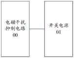
图12是本公开实施例提供的一种电子设备的结构示意图。如图12所示,该电子设备可以包括:开关电源01,以及如图2至图10任一所示的电磁干扰抑制电路00,该电磁干扰抑制电路00可以与开关电源01连接。Fig. 12 is a schematic diagram of the structure of an electronic device provided by an embodiment of the present disclosure. As shown in Fig. 12, the electronic device may include: a switching
可选的,该电子设备为显示装置。该显示装置可以为:LCD显示面板、手机、平板电脑、电视机、数码相框等任何具有显示功能的产品或部件。Optionally, the electronic device is a display device, which can be any product or component with a display function, such as an LCD display panel, a mobile phone, a tablet computer, a television, a digital photo frame, etc.
所属领域的技术人员可以清楚地了解到,为描述的方便和简洁,上述描述的电磁干扰抑制电路、各子电路和各单元的具体工作过程,可以参考前述方法实施例中的对应过程,在此不再赘述。Those skilled in the art can clearly understand that, for the convenience and brevity of description, the specific working processes of the electromagnetic interference suppression circuit, each sub-circuit and each unit described above can refer to the corresponding processes in the aforementioned method embodiment and will not be repeated here.
以上所述仅为本公开的可选实施例,并不用以限制本公开,凡在本公开的精神和原则之内,所作的任何修改、等同替换、改进等,均应包含在本公开的保护范围之内。The above description is only an optional embodiment of the present disclosure and is not intended to limit the present disclosure. Any modifications, equivalent substitutions, improvements, etc. made within the spirit and principles of the present disclosure shall be included in the protection scope of the present disclosure.
Claims (10)
Translated fromChinesePriority Applications (2)
| Application Number | Priority Date | Filing Date | Title |
|---|---|---|---|
| CN201911164314.4ACN110992863B (en) | 2019-11-25 | 2019-11-25 | Electromagnetic interference suppression circuit, driving method thereof, and electronic equipment |
| US16/999,119US11398174B2 (en) | 2019-11-25 | 2020-08-21 | Electromagnetic interference suppression circuit, method for driving same, and electronic apparatus |
Applications Claiming Priority (1)
| Application Number | Priority Date | Filing Date | Title |
|---|---|---|---|
| CN201911164314.4ACN110992863B (en) | 2019-11-25 | 2019-11-25 | Electromagnetic interference suppression circuit, driving method thereof, and electronic equipment |
Publications (2)
| Publication Number | Publication Date |
|---|---|
| CN110992863A CN110992863A (en) | 2020-04-10 |
| CN110992863Btrue CN110992863B (en) | 2023-05-30 |
Family
ID=70086446
Family Applications (1)
| Application Number | Title | Priority Date | Filing Date |
|---|---|---|---|
| CN201911164314.4AActiveCN110992863B (en) | 2019-11-25 | 2019-11-25 | Electromagnetic interference suppression circuit, driving method thereof, and electronic equipment |
Country Status (2)
| Country | Link |
|---|---|
| US (1) | US11398174B2 (en) |
| CN (1) | CN110992863B (en) |
Families Citing this family (2)
| Publication number | Priority date | Publication date | Assignee | Title |
|---|---|---|---|---|
| CN110969999B (en)* | 2019-11-25 | 2021-09-07 | 厦门天马微电子有限公司 | Electromagnetic interference weakening circuit, display panel and display device |
| CN112530350B (en) | 2020-12-18 | 2023-07-18 | 厦门天马微电子有限公司 | Display panel and display device |
Family Cites Families (15)
| Publication number | Priority date | Publication date | Assignee | Title |
|---|---|---|---|---|
| US8897039B2 (en)* | 2007-06-12 | 2014-11-25 | Bcd Semiconductor Manufacturing Limited | Method and system for pulse frequency modulated switching mode power supplies |
| CN101877531B (en)* | 2009-04-30 | 2012-11-07 | 辉芒微电子(深圳)有限公司 | Switch power supply as well as used frequency jitter generating device and method thereof |
| TWI433437B (en)* | 2011-02-01 | 2014-04-01 | Richpower Microelectronics | Jittering frequency control circuit for a switching mode power supply |
| CN103078489B (en)* | 2011-10-25 | 2015-12-16 | 昂宝电子(上海)有限公司 | The system and method reducing electromagnetic interference is shaken for utilizing switching frequency |
| CN103107719B (en)* | 2013-02-19 | 2015-10-21 | 昂宝电子(上海)有限公司 | The system and method for electromagnetic interference is reduced by by-pass cock process |
| CN103607112B (en)* | 2013-12-01 | 2016-03-02 | 西安电子科技大学 | Frequency of adaptive switch Circuit tuning |
| JP2015228761A (en)* | 2014-06-02 | 2015-12-17 | 富士通株式会社 | Power supply device and information processor |
| JP6544120B2 (en)* | 2015-07-31 | 2019-07-17 | 富士電機株式会社 | Switching power supply control circuit and switching power supply |
| CN105186856A (en)* | 2015-08-12 | 2015-12-23 | 深圳市华星光电技术有限公司 | Electromagnetic interference circuit for lowering PWM signal |
| JP6665476B2 (en)* | 2015-10-06 | 2020-03-13 | 富士電機株式会社 | Switching power supply control circuit |
| CN107181924A (en)* | 2017-07-25 | 2017-09-19 | 惠科股份有限公司 | Power supply device and display system |
| CN107294383B (en)* | 2017-06-26 | 2019-05-24 | 上海艾为电子技术股份有限公司 | A kind of Switching Power Supply |
| CN107612306A (en)* | 2017-08-25 | 2018-01-19 | 惠科股份有限公司 | Device and method for eliminating electromagnetic interference |
| US11005364B1 (en)* | 2019-12-18 | 2021-05-11 | Silanna Asia Pte Ltd | Frequency jitter utilizing a fractional valley switching controller |
| US11616433B2 (en)* | 2020-04-07 | 2023-03-28 | Texas Instruments Incorporated | Active noise filtering for switch mode power supplies |
- 2019
- 2019-11-25CNCN201911164314.4Apatent/CN110992863B/enactiveActive
- 2020
- 2020-08-21USUS16/999,119patent/US11398174B2/enactiveActive
Also Published As
| Publication number | Publication date |
|---|---|
| US20210158739A1 (en) | 2021-05-27 |
| US11398174B2 (en) | 2022-07-26 |
| CN110992863A (en) | 2020-04-10 |
Similar Documents
| Publication | Publication Date | Title |
|---|---|---|
| KR101913519B1 (en) | Shift register and driving method thereof, gate driving circuit and display device | |
| CN103684354B (en) | Ring oscillator circuit, ring oscillator and implementation method thereof | |
| CN110992863B (en) | Electromagnetic interference suppression circuit, driving method thereof, and electronic equipment | |
| CN105845183B (en) | Shift-register circuit, array substrate and display device | |
| CN102594272B (en) | Circuit for reducing electromagnetic interference of class-D audio-frequency power amplifier | |
| TWI439851B (en) | Low power consumption circuit and method for reducing power consumption | |
| Pakbaznia et al. | Design of a tri-modal multi-threshold CMOS switch with application to data retentive power gating | |
| CN207490762U (en) | A kind of rapid pressure charge pump circuit | |
| CN106452394A (en) | Clock switching structure having automatic resetting function | |
| CN101197531A (en) | Capacitance-controlled digital frequency modulation circuit | |
| WO2020078209A1 (en) | Frequency modulation device, switching power supply and frequency modulation method therefor | |
| CN113972902B (en) | Clock signal generating circuit, clock signal generating method and electronic equipment | |
| ur Rahman et al. | Quasi-resonant clocking: Continuous voltage-frequency scalable resonant clocking system for dynamic voltage-frequency scaling systems | |
| CN107947581B (en) | Adaptive power width modulation circuit for switching capacity DC-DC converter | |
| CN112640288B (en) | Positive and negative pressure coding circuit, chip, active pen and coding method | |
| CN105094268A (en) | Control system for reducing clock current in standby state of system | |
| CN110601528A (en) | Charge pump and storage device | |
| CN115276615A (en) | Clock signal frequency multiplier circuit outputting burr-free low duty ratio error | |
| US9571263B2 (en) | Integrated circuit incorporating a low power data retiming circuit | |
| CN108365836B (en) | Novel relaxation oscillator circuit | |
| CN109947167B (en) | Negative pressure linear voltage stabilizer | |
| CN113050786A (en) | A standby system and display device | |
| CN219304699U (en) | Spread spectrum clock generating circuit and DCDC switching power supply circuit | |
| WO2021023293A1 (en) | Charging circuit, charging chip, terminal, and charging system | |
| CN201854257U (en) | Mixed delay circuit module |
Legal Events
| Date | Code | Title | Description |
|---|---|---|---|
| PB01 | Publication | ||
| PB01 | Publication | ||
| SE01 | Entry into force of request for substantive examination | ||
| SE01 | Entry into force of request for substantive examination | ||
| GR01 | Patent grant | ||
| GR01 | Patent grant |