CN110870013A - Multilevel signaling in memory with wide system interface - Google Patents
Multilevel signaling in memory with wide system interfaceDownload PDFInfo
- Publication number
- CN110870013A CN110870013ACN201880045340.2ACN201880045340ACN110870013ACN 110870013 ACN110870013 ACN 110870013ACN 201880045340 ACN201880045340 ACN 201880045340ACN 110870013 ACN110870013 ACN 110870013A
- Authority
- CN
- China
- Prior art keywords
- array
- memory cells
- memory
- signal
- controller
- Prior art date
- Legal status (The legal status is an assumption and is not a legal conclusion. Google has not performed a legal analysis and makes no representation as to the accuracy of the status listed.)
- Pending
Links
Images


Classifications
- G—PHYSICS
- G11—INFORMATION STORAGE
- G11C—STATIC STORES
- G11C11/00—Digital stores characterised by the use of particular electric or magnetic storage elements; Storage elements therefor
- G11C11/56—Digital stores characterised by the use of particular electric or magnetic storage elements; Storage elements therefor using storage elements with more than two stable states represented by steps, e.g. of voltage, current, phase, frequency
- G11C11/565—Digital stores characterised by the use of particular electric or magnetic storage elements; Storage elements therefor using storage elements with more than two stable states represented by steps, e.g. of voltage, current, phase, frequency using capacitive charge storage elements
- G—PHYSICS
- G11—INFORMATION STORAGE
- G11C—STATIC STORES
- G11C5/00—Details of stores covered by group G11C11/00
- G11C5/02—Disposition of storage elements, e.g. in the form of a matrix array
- G—PHYSICS
- G11—INFORMATION STORAGE
- G11C—STATIC STORES
- G11C5/00—Details of stores covered by group G11C11/00
- G11C5/02—Disposition of storage elements, e.g. in the form of a matrix array
- G11C5/025—Geometric lay-out considerations of storage- and peripheral-blocks in a semiconductor storage device
- G—PHYSICS
- G11—INFORMATION STORAGE
- G11C—STATIC STORES
- G11C5/00—Details of stores covered by group G11C11/00
- G11C5/02—Disposition of storage elements, e.g. in the form of a matrix array
- G11C5/04—Supports for storage elements, e.g. memory modules; Mounting or fixing of storage elements on such supports
- G—PHYSICS
- G11—INFORMATION STORAGE
- G11C—STATIC STORES
- G11C7/00—Arrangements for writing information into, or reading information out from, a digital store
- G11C7/10—Input/output [I/O] data interface arrangements, e.g. I/O data control circuits, I/O data buffers
- G11C7/1003—Interface circuits for daisy chain or ring bus memory arrangements
- G—PHYSICS
- G11—INFORMATION STORAGE
- G11C—STATIC STORES
- G11C7/00—Arrangements for writing information into, or reading information out from, a digital store
- G11C7/10—Input/output [I/O] data interface arrangements, e.g. I/O data control circuits, I/O data buffers
- G11C7/1006—Data managing, e.g. manipulating data before writing or reading out, data bus switches or control circuits therefor
- G—PHYSICS
- G11—INFORMATION STORAGE
- G11C—STATIC STORES
- G11C7/00—Arrangements for writing information into, or reading information out from, a digital store
- G11C7/10—Input/output [I/O] data interface arrangements, e.g. I/O data control circuits, I/O data buffers
- G11C7/1048—Data bus control circuits, e.g. precharging, presetting, equalising
- G—PHYSICS
- G11—INFORMATION STORAGE
- G11C—STATIC STORES
- G11C7/00—Arrangements for writing information into, or reading information out from, a digital store
- G11C7/10—Input/output [I/O] data interface arrangements, e.g. I/O data control circuits, I/O data buffers
- G11C7/1051—Data output circuits, e.g. read-out amplifiers, data output buffers, data output registers, data output level conversion circuits
- G11C7/1057—Data output buffers, e.g. comprising level conversion circuits, circuits for adapting load
- G—PHYSICS
- G11—INFORMATION STORAGE
- G11C—STATIC STORES
- G11C7/00—Arrangements for writing information into, or reading information out from, a digital store
- G11C7/10—Input/output [I/O] data interface arrangements, e.g. I/O data control circuits, I/O data buffers
- G11C7/1078—Data input circuits, e.g. write amplifiers, data input buffers, data input registers, data input level conversion circuits
- G11C7/1084—Data input buffers, e.g. comprising level conversion circuits, circuits for adapting load
- G—PHYSICS
- G11—INFORMATION STORAGE
- G11C—STATIC STORES
- G11C7/00—Arrangements for writing information into, or reading information out from, a digital store
- G11C7/10—Input/output [I/O] data interface arrangements, e.g. I/O data control circuits, I/O data buffers
- G11C7/1078—Data input circuits, e.g. write amplifiers, data input buffers, data input registers, data input level conversion circuits
- G11C7/1096—Write circuits, e.g. I/O line write drivers
- H—ELECTRICITY
- H04—ELECTRIC COMMUNICATION TECHNIQUE
- H04L—TRANSMISSION OF DIGITAL INFORMATION, e.g. TELEGRAPHIC COMMUNICATION
- H04L25/00—Baseband systems
- H04L25/38—Synchronous or start-stop systems, e.g. for Baudot code
- H04L25/40—Transmitting circuits; Receiving circuits
- H04L25/49—Transmitting circuits; Receiving circuits using code conversion at the transmitter; using predistortion; using insertion of idle bits for obtaining a desired frequency spectrum; using three or more amplitude levels ; Baseband coding techniques specific to data transmission systems
- H04L25/4917—Transmitting circuits; Receiving circuits using code conversion at the transmitter; using predistortion; using insertion of idle bits for obtaining a desired frequency spectrum; using three or more amplitude levels ; Baseband coding techniques specific to data transmission systems using multilevel codes
- H04L25/4919—Transmitting circuits; Receiving circuits using code conversion at the transmitter; using predistortion; using insertion of idle bits for obtaining a desired frequency spectrum; using three or more amplitude levels ; Baseband coding techniques specific to data transmission systems using multilevel codes using balanced multilevel codes
- H04L25/4921—Transmitting circuits; Receiving circuits using code conversion at the transmitter; using predistortion; using insertion of idle bits for obtaining a desired frequency spectrum; using three or more amplitude levels ; Baseband coding techniques specific to data transmission systems using multilevel codes using balanced multilevel codes using quadrature encoding, e.g. carrierless amplitude-phase coding
Landscapes
- Engineering & Computer Science (AREA)
- Computer Hardware Design (AREA)
- Physics & Mathematics (AREA)
- Spectroscopy & Molecular Physics (AREA)
- Computer Networks & Wireless Communication (AREA)
- Signal Processing (AREA)
- Microelectronics & Electronic Packaging (AREA)
- Dram (AREA)
- Electrotherapy Devices (AREA)
- Input Circuits Of Receivers And Coupling Of Receivers And Audio Equipment (AREA)
- Dc Digital Transmission (AREA)
Abstract
Translated fromChinese
Description
Translated fromChinese交叉参考cross reference
本专利申请案主张由霍利斯(Hollis)等在于2017年12月26日申请的标题为“在具有宽系统接口的存储器中的多电平信令(Multi-Level Signaling in Memory with WideSystem Interface)”的第15/854,600号美国专利申请案的优先权,所述申请案主张由霍利斯等人在2017年8月7日申请的标题为“在具有宽系统接口的存储器中的多电平信令”的第62/542,160号美国临时专利申请案的权益,所述申请案中的每一者以引用的方式明确并入本文中。This patent application claims "Multi-Level Signaling in Memory with Wide System Interface", filed by Hollis et al. on December 26, 2017 ” of U.S. Patent Application Serial No. 15/854,600, which claims priority of U.S. Patent Application Serial No. 15/854,600, filed on Aug. 7, 2017 by Hollis et al. Signaling" of the benefit of US Provisional Patent Application No. 62/542,160, each of which is expressly incorporated herein by reference.
背景技术Background technique
下文大体上涉及使用存储器装置的多电平信令且更特定来说涉及在包含宽系统接口的存储器装置中的多电平信令。The following relates generally to multi-level signaling using memory devices and more particularly to multi-level signaling in memory devices that include wide system interfaces.
存储器装置广泛用于将信息存储于各种电子装置中,例如计算机、无线通信装置、相机、数字显示器及类似物。通过编程存储器装置的不同状态来存储信息。举例来说,二进制装置具有两个状态,其通常由逻辑“1”或逻辑“0”表示。在其它系统中,可存储两个以上状态。为存取所存储的信息,电子装置的组件可读取或感测存储器装置中的经存储状态。为存储信息,电子装置的组件可将状态写入或编程于存储器装置中。Memory devices are widely used to store information in various electronic devices, such as computers, wireless communication devices, cameras, digital displays, and the like. Information is stored by programming different states of the memory device. For example, a binary device has two states, typically represented by a logic "1" or a logic "0." In other systems, more than two states may be stored. To access the stored information, components of the electronic device may read or sense the stored state in the memory device. To store information, components of an electronic device may write or program state into a memory device.
存在多种类型的存储器装置,包含磁性硬盘、随机存取存储器(RAM)、只读存储器(ROM)、动态RAM(DRAM)、同步动态RAM(SDRAM)、铁电RAM(FeRAM)、磁性RAM(MRAM)、电阻式RAM(RRAM)、快闪存储器、相变存储器(PCM)等。存储器装置可为易失性或非易失性。非易失性存储器(例如,FeRAM)可甚至在无外部电源的情况下维持其所存储逻辑状态达延长时段。易失性存储器装置(例如,DRAM)可随时间丢失其所存储状态,除非其由外部电源周期性刷新。FeRAM可使用类似于易失性存储器的装置架构,但可归因于使用铁电电容器作为存储装置而具有非易失性质。因此,相较于其它非易失性及易失性存储器装置,FeRAM装置可具有改进性能。Various types of memory devices exist, including magnetic hard disks, random access memory (RAM), read only memory (ROM), dynamic RAM (DRAM), synchronous dynamic RAM (SDRAM), ferroelectric RAM (FeRAM), magnetic RAM ( MRAM), resistive RAM (RRAM), flash memory, phase change memory (PCM), etc. Memory devices may be volatile or non-volatile. Non-volatile memory (eg, FeRAM) can maintain its stored logic state for extended periods of time even without an external power source. A volatile memory device (eg, DRAM) can lose its stored state over time unless it is periodically refreshed by an external power source. FeRAM may use a device architecture similar to volatile memory, but may have non-volatile properties due to the use of ferroelectric capacitors as storage devices. Accordingly, FeRAM devices may have improved performance compared to other non-volatile and volatile memory devices.
一般来说,改进存储器装置可包含增加存储器单元密度、增加读取/写入速度、增加可靠性、增加数据保持、减小功率消耗或减小制造成本以及其它度量。In general, improving memory devices may include increasing memory cell density, increasing read/write speed, increasing reliability, increasing data retention, reducing power consumption, or reducing manufacturing cost, among other metrics.
附图说明Description of drawings
图1说明根据本发明的实施例的支持具有宽系统接口的存储器中的多电平信令的存储器装置的实例。1 illustrates an example of a memory device supporting multi-level signaling in memory with a wide system interface in accordance with an embodiment of the present invention.
图2说明根据本发明的实施例的支持具有宽系统接口的存储器中的多电平信令的眼图的实例。2 illustrates an example of an eye diagram supporting multi-level signaling in memory with a wide system interface in accordance with an embodiment of the present invention.
图3说明根据本发明的实施例的支持具有宽系统接口的存储器中的多电平信令的发射电路的实例。3 illustrates an example of a transmit circuit supporting multi-level signaling in memory with a wide system interface in accordance with an embodiment of the present invention.
图4说明根据本发明的实施例的支持具有宽系统接口的存储器中的多电平信令的接收器的实例。4 illustrates an example of a receiver supporting multi-level signaling in memory with a wide system interface in accordance with an embodiment of the present invention.
图5说明根据本发明的实施例的支持具有宽系统接口的存储器中的多电平信令的存储器装置的实例。5 illustrates an example of a memory device supporting multi-level signaling in memory with a wide system interface in accordance with an embodiment of the present invention.
图6展示根据本发明的实施例的支持具有宽系统接口的存储器中的多电平信令的装置的框图。6 shows a block diagram of a device supporting multi-level signaling in memory with a wide system interface in accordance with an embodiment of the invention.
图7说明根据本发明的实施例的包含支持具有宽系统接口的存储器中的多电平信令的存储器控制器的系统的框图。7 illustrates a block diagram of a system including a memory controller supporting multi-level signaling in memory with a wide system interface in accordance with an embodiment of the invention.
图8说明根据本发明的实施例的用于具有宽系统接口的存储器中的多电平信令的方法。8 illustrates a method for multi-level signaling in memory with a wide system interface in accordance with an embodiment of the present invention.
具体实施方式Detailed ways
一些存储器装置可在所连接装置(例如,存储器单元阵列与处理器)之间使用宽通信信道以传达数据(例如,高带宽存储器(HBM))。在一些情况中,这些宽通信信道包含较大数目个电阻式信道。由于每一信道是电阻式的,所以随着数据传送频率增加,传送数据所需的功率相对于频率以非线性方式增加。此类特性可带来实际频率上限,其可用于通过电阻式信道在给定发射功率量的情况下发射数据。Some memory devices may use wide communication channels between connected devices (eg, an array of memory cells and a processor) to communicate data (eg, high bandwidth memory (HBM)). In some cases, these wide communication channels include a larger number of resistive channels. Since each channel is resistive, as the data transmission frequency increases, the power required to transmit data increases in a non-linear fashion with respect to frequency. Such characteristics can introduce a practical upper frequency limit that can be used to transmit data over a resistive channel for a given amount of transmit power.
本文中提供使用多电平信令增加跨存储器装置中的较大数目个信道的数据传送速度的技术。此多电平信令可经配置以增加数据传送速度而不增加数据传送频率及/或所传达数据的发射功率。多电平信令方案的实例可为脉冲振幅调制(PAM),例如PAM4或PAM8。多电平信号的每一独有符号可经配置以表示多个数据位。Provided herein are techniques for increasing data transfer speed across a larger number of channels in a memory device using multi-level signaling. Such multi-level signaling can be configured to increase data transfer speed without increasing data transfer frequency and/or transmit power of the data communicated. An example of a multi-level signaling scheme may be pulse amplitude modulation (PAM), such as PAM4 or PAM8. Each unique symbol of a multilevel signal can be configured to represent multiple data bits.
下文在存储器装置的内容背景中进一步描述上文介绍的本发明的特征。接着,针对支持具有宽系统接口的存储器中的多电平信令的存储器装置描述特定实例。本发明的这些及其它特征进一步通过与多电平信令相关的设备图、系统图及流程图说明且参考其加以描述。The features of the invention introduced above are further described below in the context of memory devices. Next, specific examples are described for memory devices that support multi-level signaling in memory with wide system interfaces. These and other features of the present invention are further illustrated by and described with reference to device diagrams, system diagrams, and flow diagrams related to multilevel signaling.
图1说明根据本发明的各种实例的实例存储器装置100。存储器装置100还可称为电子存储器设备。存储器装置100可经配置以利用多电平信令以在存储器装置100的各种组件之间传达数据。多电平信令的一些实例可包含PAM信令,例如PAM4信令、PAM8信令等。存储器装置100可包含存储器单元阵列105、控制器110、多个信道115、信令接口120、其它组件或其组合。1 illustrates an
存储器装置100可使用多电平信令以增加使用频率资源的给定带宽发射的信息量。在二进制信令中,信号的两个符号(例如,两个电压电平)用于表示至多两个逻辑状态(例如,逻辑状态‘0’或逻辑状态‘1’)。在多电平信令中,较大符号库可用于表示数据。每一符号可表示两个以上逻辑状态(例如,具有多个位的逻辑状态)。举例来说,如果信号能够具有四个独有符号,那么信号可用于表示至多四个逻辑状态(例如,‘00’、‘01’、‘10’及‘11’)。因此,可将多个数据位压缩成单个符号,借此增加使用给定带宽传达的数据量。
在多电平信令的一些情况中,信号的振幅可用于产生不同符号。举例来说,第一振幅电平可表示‘00’,第二振幅电平可表示‘01’,第三振幅电平可表示‘10’,且第四振幅电平可表示‘11’。一些多电平信令方案的一个缺点是符号可由小于二进制信令方案中的符号的电压分离。较小电压分离可使多电平信令方案更易具有由噪声或其它方面引起的错误。然而,可通过增加所发射信号的峰值对峰值发射功率而扩展多电平信令方案中的符号的电压分离。然而,在一些状况中,峰值对峰值发射功率的此增加可归因于固定电力供应电压、固定信号功率要求或其它因素而是不可能或困难的。因此,为实施多电平信令,在与二进制信令方案相比时,发射器可利用更多电力及/或接收器可易于具有增加错误率。In some cases of multi-level signaling, the amplitude of the signal can be used to generate different symbols. For example, a first amplitude level can represent '00', a second amplitude level can represent '01', a third amplitude level can represent '10', and a fourth amplitude level can represent '11'. One disadvantage of some multi-level signaling schemes is that symbols can be separated by less voltage than symbols in binary signaling schemes. Smaller voltage separation can make multi-level signaling schemes more prone to errors caused by noise or otherwise. However, the voltage separation of symbols in a multi-level signaling scheme can be extended by increasing the peak-to-peak transmit power of the transmitted signal. However, in some situations, this increase in peak-to-peak transmit power may be impossible or difficult due to fixed power supply voltage, fixed signal power requirements, or other factors. Thus, to implement multi-level signaling, a transmitter may utilize more power and/or a receiver may tend to have an increased error rate when compared to a binary signaling scheme.
多电平信号(有时称为多符号信号)可为使用包含三个或三个以上独有符号以表示数据(例如,两个或两个以上数据位)的调制方案调制的信号。多电平信号可为使用调制方案调制的M进位信号的实例,其中M大于或等于3,其中M表示调制方案中可能的独有符号、电平或条件的数目。在一些例子中,多电平信号或多电平调制方案可称为非二进制信号或非二进制调制方案。与多电平信号相关的多电平(或M进位)调制方案的实例可包含(但不限于)脉冲振幅调制(例如,PAM4、PAM8)、正交振幅调制(QAM)、正交相移键控(QPSK)及/或其它。A multilevel signal (sometimes referred to as a multisymbol signal) may be a signal modulated using a modulation scheme that includes three or more unique symbols to represent data (eg, two or more data bits). A multilevel signal may be an example of an M-ary signal modulated using a modulation scheme, where M is greater than or equal to 3, where M represents the number of unique symbols, levels or conditions possible in the modulation scheme. In some examples, a multi-level signal or multi-level modulation scheme may be referred to as a non-binary signal or non-binary modulation scheme. Examples of multilevel (or M-carry) modulation schemes associated with multilevel signals may include, but are not limited to, pulse amplitude modulation (eg, PAM4, PAM8), quadrature amplitude modulation (QAM), quadrature phase shift keying control (QPSK) and/or others.
二进制电平信号(有时称为二进制符号信号)可为使用调制方案调制的信号,其包含两个独有符号以表示一个数据位。二进制电平信号可为M进位调制方案的实例,其中M小于或等于2。与二进制电平信号相关的二进制电平调制方案的实例包含(但不限于)不归零(NRZ)、单极编码、双极编码、曼彻斯特编码、PAM2及/或其它。A binary level signal (sometimes referred to as a binary symbol signal) may be a signal modulated using a modulation scheme that contains two unique symbols to represent one data bit. The binary level signal may be an example of an M-ary modulation scheme, where M is less than or equal to two. Examples of binary level modulation schemes related to binary level signals include, but are not limited to, non-return to zero (NRZ), unipolar coding, bipolar coding, Manchester coding, PAM2, and/or others.
存储器单元阵列105的每一存储器单元可编程以存储不同状态。举例来说,每一存储器单元可编程以存储两个或两个以上逻辑状态(例如,逻辑‘0’、逻辑‘1’、逻辑‘00’、逻辑‘01’、逻辑‘10’、逻辑‘11’等)。存储器单元可将表示可编程状态的电荷存储于电容器中;举例来说,带电及不带电电容器可分别表示两个逻辑状态。存储器单元阵列105的存储器单元可使用任何数目个存储媒体,包含DRAM、FeRAM、PCM或其它类型的存储器单元。DRAM存储器单元可包含具有作为绝缘材料的电介质材料的电容器。举例来说,电介质材料可具有线性或顺电电极化性质且铁电存储器单元可包含具有作为绝缘材料的铁电材料的电容器。在其中存储媒体包含FeRAM的例子中,铁电电容器的不同电荷电平可表示不同逻辑状态。Each memory cell of
存储器单元阵列105可为或包含三维(3D)阵列,其中多个二维(2D)阵列或多个存储器单元彼此叠置。与2D阵列相比,此配置可增加可形成于单个晶片或衬底上的存储器单元的数目。此又可减小生产成本或增加存储器阵列的性能或两者。阵列的每一电平可经对准或定位,使得存储器单元可跨每一电平近似彼此对准,从而形成存储器单元堆叠。The
在一些实例中,存储器单元阵列105可包含存储器单元、字线、数字线及感测组件。在一些实例中,存储器单元阵列105可包含板极线(例如,在FeRAM的情况中)。存储器单元阵列105的存储器单元可包含选择组件及逻辑存储组件,例如包含第一板极、单元板极、第二板极及单元底部的电容器。单元板极及单元底部可通过定位于其之间的绝缘材料(例如,电介质、铁电或PCM材料)电容性地耦合。In some examples,
可使用字线、数字线及/或板极线的各种组合(例如,在读取操作、写入操作或其它操作期间)存取存储器单元阵列105的存储器单元。在一些情况中,一些存储器单元可与其它存储器单元共享存取线(例如,数字线、字线、板极线)。举例来说,相同列中的存储器单元可共享数字线,相同行中的存储器单元可共享字线,且相同区段、块、层叠或多个层叠中的存储器单元可共享板极线。如上文描述,可通过使存储器单元的电容器充电或放电而存储各种状态。The memory cells of
可通过操作各种元件而读取或感测存储器单元的电容器的所存储状态。电容器可与数字线电子通信。电容器可在撤销激活选择组件时与数字线隔离,且电容器可在(例如,通过字线)激活选择组件时连接到数字线。激活选择组件可称为选择存储器单元。在一些情况中,选择组件可为晶体管且其操作可通过施加电压到晶体管栅极而加以控制,其中电压量值大于晶体管的阈值量值。字线可激活选择组件;举例来说,施加到字线的晶体管栅极的电压可连接存储器单元的电容器与数字线。The stored state of the capacitors of the memory cells can be read or sensed by manipulating various elements. The capacitors are in electronic communication with the digital lines. The capacitor can be isolated from the digit line when the select component is deactivated, and the capacitor can be connected to the digit line when the select component is activated (eg, through a word line). Activating a selection component may be referred to as selecting a memory cell. In some cases, the selection component can be a transistor and its operation can be controlled by applying a voltage to the transistor gate, wherein the voltage magnitude is greater than the transistor's threshold magnitude. A word line can activate selection components; for example, a voltage applied to the gate of a transistor of the word line can connect the capacitor of the memory cell to the digit line.
在一些实例中,数字线的电压改变可取决于其本征电容。即,随着电荷流动通过数字线,某有限电荷可存储于数字线中且所得电压取决于本征电容。本征电容可取决于物理特性,包含数字线的尺寸。数字线可连接存储器单元阵列105的许多存储器单元,因此数字线可具有导致不可忽略电容(例如,约几皮法拉(pF))的长度。接着,可由感测组件比较数字线的所得电压与参考电压(例如,参考线的电压),以便确定存储器单元中的所存储逻辑状态。可使用其它感测过程。In some examples, the voltage change of the digit line may depend on its intrinsic capacitance. That is, as charge flows through the digit line, some finite charge can be stored in the digit line and the resulting voltage depends on the intrinsic capacitance. Intrinsic capacitance can depend on physical characteristics, including the size of the digit lines. The digit lines may connect many memory cells of the
感测组件可包含各种晶体管或放大器以检测及放大信号的差异,此可称为锁存。感测组件可包含感测放大器,其接收及比较数字线的电压与参考线(其可为参考电压)。可基于比较将感测放大器输出驱动到更高(例如,正)或更低(例如,负或接地)供应电压。举例来说,如果数字线具有高于参考线的电压,那么可将感测放大器输出驱动到正供应电压。The sensing component may include various transistors or amplifiers to detect and amplify the difference in the signal, which may be referred to as a latch. The sense component may include a sense amplifier that receives and compares the voltage of the digit line to a reference line (which may be a reference voltage). The sense amplifier output can be driven to a higher (eg, positive) or lower (eg, negative or ground) supply voltage based on the comparison. For example, if the digit line has a higher voltage than the reference line, the sense amplifier output can be driven to a positive supply voltage.
在一些情况中,感测放大器可将数字线驱动到供应电压。感测组件接着可锁存感测放大器的输出及/或数字线的电压,其可用于确定存储器单元中的所存储状态(例如,逻辑,‘1’)。替代地,举例来说,如果数字线具有高于参考线的电压,那么可将感测放大器输出驱动到负或接地电压。感测组件可类似地锁存感测放大器输出以确定存储器单元中的所存储状态(例如,逻辑‘0’)。可接着例如通过列解码器输出存储器单元的锁存逻辑状态。In some cases, a sense amplifier can drive the digit lines to the supply voltage. The sense component can then latch the output of the sense amplifier and/or the voltage of the digit line, which can be used to determine the stored state (eg, logical, '1') in the memory cell. Alternatively, for example, if the digit line has a higher voltage than the reference line, the sense amplifier output can be driven to a negative or ground voltage. The sense component can similarly latch the sense amplifier output to determine the stored state (eg, logic '0') in the memory cell. The latched logic state of the memory cell may then be output, eg, by a column decoder.
为写入存储器单元,可跨存储器单元的电容器施加电压。可使用各种方法写入存储器单元。在一个实例中,可通过字线激活选择组件,以便将电容器电连接到数字线。可通过控制单元板极(例如,通过板极线)及单元底部(例如,通过数字线)的电压而跨电容器施加电压。为写入逻辑‘0’,单元板极可为高(例如,电压电平可增加而高于预定电压(其为“高”电压))。即,可将正电压施加到板极线,且单元底部可为低(例如,虚拟接地或施加负电压到数位线)。可执行相反过程以写入逻辑‘1’,其中单元板极可为低且单元底部可为高。To write to a memory cell, a voltage may be applied across the memory cell's capacitor. Memory cells can be written to using various methods. In one example, select components can be activated through the word lines to electrically connect the capacitors to the digit lines. A voltage may be applied across the capacitor by controlling the voltage at the cell plates (eg, through the plate lines) and the bottom of the cell (eg, through the digit lines). To write a logic '0', the cell plate can be high (eg, the voltage level can be increased above a predetermined voltage (which is a "high" voltage)). That is, a positive voltage can be applied to the plate line, and the bottom of the cell can be low (eg, virtual ground or negative voltage applied to the digit line). The reverse process can be performed to write a logic '1', where the cell plate can be low and the cell bottom can be high.
控制器110可通过各种组件(例如,行解码器、列解码器及感测组件)控制存储器单元阵列105中的存储器单元的操作(例如,读取、写入、重写、刷新、放电等)。在一些情况中,行解码器、列解码器及感测组件中的一或多者可与控制器110共置。控制器110可产生行及列地址信号,以便激活所要字线及数字线。在其它实例中,控制器110可产生及控制在存储器装置100的操作期间使用的各种电压或电流。举例来说,控制器110可在存取一或多个存储器单元之后将放电电压施加到字线或数位线。一般来说,本文中论述的经施加电压或电流的振幅、形状或持续时间可经调整或变化且可针对操作存储器装置100时论述的各种操作而不同。此外,可同时存取存储器单元阵列105内的一个、多个或全部存储器单元。举例来说,可在复位操作期间同时存取存储器单元阵列105的多个存储器单元或全部存储器单元,其中多个存储器单元或全部存储器单元可设置为单个逻辑状态(例如,逻辑“0”)。Controller 110 may control operations (eg, read, write, rewrite, refresh, discharge, etc.) of memory cells in
多个信道115中的每一者可经配置以耦合存储器单元阵列105与控制器110。在一些实例中,多个信道115中的每一者可称为多个支路。在一些存储器装置中,可通过跨多个信道115传送的数据速率限制存储器装置与主机装置(例如,个人计算机或其它计算装置)之间的数据传送速度。在一些实例中,存储器装置100可包含较大数目个高电阻信道。通过增加信道数目,可增加存储器装置100中传送的数据量而不增加数据传送速度。在一些实例中,多个信道115可称为宽系统接口。多个信道115中的每一者可为定位于存储器单元阵列105与控制器110之间的内插器的部分。在一些实例中,信道115中的一或多者可为单向的,且在其它实例中,信道115中的一或多者可为双向的。Each of the plurality of
在一些实例中,至少一些(且在一些情况中,每一者)信令接口120可产生及/或解码使用多个信道115传达的信号。信令接口120可相关联于与多个信道115耦合的每一组件。信令接口120可经配置以产生及/或解码多电平信号、二进制信号或两者(例如,同时)。每一信令接口120可包含驱动器125及接收器130。在一些实例中,每一驱动器125可称为多支路驱动器。In some examples, at least some (and in some cases, each) signaling
每一驱动器125可经配置以基于包含多个位的逻辑状态产生多电平信号。举例来说,驱动器125可使用PAM4信令技术(或其它类型的多电平信令技术)以产生具有对应于所述逻辑状态的振幅的信号。驱动器125可经配置以使用单个输入线接收数据。在一些情况中,驱动器125可包含用于第一数据位(例如,最高有效位)的第一输入线、用于第二数据位(例如,最低有效位)的第二输入线。在一些境况中,驱动器125可经配置以产生二进制电平信号(例如,NRZ信号)。在一些情况中,驱动器125可使用单端信令以产生多电平信号。在此类情况中,可在不具有差分的情况下发射多电平信号。Each
每一接收器130可经配置以确定由使用多个信道115接收的多电平信号的符号表示的逻辑状态。在一些情况中,接收器130可确定所接收多电平信号的振幅。基于所确定振幅,接收器130可确定由多电平信号表示的逻辑状态。接收器130可经配置以使用单个输出线输出数据。在一些情况中,接收器130可包含用于第一数据位(例如,最高有效位)的第一输出线、用于第二数据位(例如,最低有效位)的第二输出线。在一些境况中,接收器130可经配置以解码二进制电平信号(例如,NRZ信号)。举例来说,接收器130中的每一者可经由多个信道115与发射器(未说明)耦合。信道115中的每一者可经配置以输出包含多个位的数据,且控制器110可经配置以确定数据输出之间的输出阻抗偏移。一或多个晶体管(例如,未单独说明)可经配置以调整多个信道115中的一或多者的电阻电平。此调整可至少部分基于所确定输出阻抗偏移。Each
在一些情况中,信令接口120中的每一者可经配置以选择性地产生及/或解码不同类型的信号(例如,NRZ信号、PAM4信号、PAM8信号等)。可基于存储器装置100的操作环境使用不同类型的信号。举例来说,二进制信令可使用少于多电平信令的功率且可在功率消耗驱动性能考虑时使用。可用于确定应使用哪种类型的信令的其它性能因素可包含时钟考虑、数据选通(DQS)考虑、电路能力、带宽考虑、抖动考虑或其组合。在一些情况中,控制器110可经配置以选择信号类型,且信令接口120可经配置以基于从控制器110接收的指令实施选择。在一些情况中,信令接口120中的每一者可经配置以实施编码功能,例如错误检测程序、错误校正程序、数据总线反转程序或其组合。In some cases, each of signaling
在一些情况中,信令接口120可经配置以同时传达多电平信号及二进制信号。在此类情况中,信令接口120可包含一组以上驱动器125及接收器130。举例来说,信令接口120可经配置以使用第一组信道115使用二进制电平信号传达第一组数据(例如,控制信号),同时使用第二组信道115使用多电平信号传达第二组数据(例如,用户信息)。In some cases, signaling
图2说明根据本发明的各种实施例的表示多电平信号的眼图200的实例。眼图200可用于指示高速发射中的信号质量且可表示信号的四个符号(例如,‘00’、‘01’、‘10’或‘11’)。在一些实例中,四个符号中的每一者可由不同电压振幅(例如,振幅205-a、205-b、205-c、205-d)表示。在其它实例中,眼图200可表示PAM4信号,其可用于在存储器装置(例如,如参考图1描述的存储器装置100)中传达数据。眼图200可用于提供信号完整性的健康状况的视觉指示且可指示数据信号的噪声容限。噪声容限可例如是指信号超过振幅205的理想边界的量。2 illustrates an example of an eye diagram 200 representing a multi-level signal in accordance with various embodiments of the invention. The eye diagram 200 may be used to indicate signal quality in high-speed transmission and may represent four symbols of the signal (eg, '00', '01', '10', or '11'). In some examples, each of the four symbols may be represented by a different voltage amplitude (eg, amplitudes 205-a, 205-b, 205-c, 205-d). In other examples, eye diagram 200 may represent a PAM4 signal, which may be used to communicate data in a memory device (eg,
为产生眼图200,示波器或其它计算装置可根据取样周期210(例如,单位时间间隔或位周期)对数字信号取样。取样周期210可由与所测量信号的发射相关联的时钟定义。在一些实例中,示波器或其它计算装置可在取样周期210期间测量信号的电压电平以形成迹线215。噪声及其它因素可导致从根据一组理想阶梯函数导出的信号测量的迹线215。通过叠对多个迹线215,可确定关于所测量信号的各种特性。举例来说,眼图200可用于识别通信信号的数个特性,例如抖动、串扰、电磁干扰(EMI)、信号损耗、信噪比(SNR)、其它特性或其组合。闭眼可指示噪声及/或不可预测信号或其它问题。To generate eye diagram 200, an oscilloscope or other computing device may sample the digital signal according to a sampling period 210 (eg, a unit time interval or bit period). The sampling period 210 may be defined by a clock associated with the transmission of the measured signal. In some examples, an oscilloscope or other computing device may measure the voltage level of the signal during sampling period 210 to form trace 215 . Noise and other factors can result in traces 215 measured from signals derived from a set of ideal step functions. By overlaying multiple traces 215, various characteristics about the measured signal can be determined. For example, eye diagram 200 may be used to identify several characteristics of a communication signal, such as jitter, crosstalk, electromagnetic interference (EMI), signal loss, signal-to-noise ratio (SNR), other characteristics, or combinations thereof. Closing eyes may indicate noise and/or unpredictable signals or other problems.
在一些实例中,眼图200可指示宽度220。眼图200中的眼的宽度220可用于指示所测量信号的时序同步或所测量信号的抖动效应。在一些实例中,比较宽度220与取样周期210可提供所测量信号的SNR测量。眼图中的每一眼可基于所测量信号的特性而具有独有宽度。各种编码及解码技术可用于修改所测量信号的宽度220。In some examples, eye diagram 200 may indicate width 220 . The width 220 of the eye in the eye diagram 200 may be used to indicate timing synchronization of the measured signal or jitter effects of the measured signal. In some examples, comparing width 220 to sampling period 210 may provide a SNR measurement of the measured signal. Each eye in the eye diagram can have a unique width based on the characteristics of the signal being measured. Various encoding and decoding techniques can be used to modify the width 220 of the measured signal.
在其它实例中,眼图200可指示用于确定由所测量信号的符号表示的逻辑状态的值的取样时间225(例如,理想取样时间)。举例来说,确定所测量信号的取样数据的正确时间(例如,时序同步)对于最小化信号检测中的错误率可为重要的。举例来说,如果计算装置在转变时间(例如,上升时间230或下降时间235)期间对信号取样,那么可由解码器将错误引入到由信号的符号表示的数据中。各种编码及解码技术可用于修改所测量信号的理想取样时间225。In other examples, the eye diagram 200 may indicate a sampling time 225 (eg, an ideal sampling time) for determining the value of the logic state represented by the symbol of the measured signal. For example, determining the correct time (eg, timing synchronization) of the sampled data of the measured signal can be important to minimize the error rate in signal detection. For example, if the computing device samples the signal during transition times (eg, rise time 230 or fall time 235), errors may be introduced by the decoder into the data represented by the symbols of the signal. Various encoding and decoding techniques can be used to modify the ideal sampling time 225 of the measured signal.
眼图200可用于识别从第一振幅205转变到第二振幅205的上升时间230及/或下降时间235。迹线215在上升时间230或下降时间235期间的斜率可指示信号对时序错误的敏感度及其它方面。举例来说,迹线215的斜率越陡(例如,上升时间230及/或下降时间235越小),振幅205之间的转变越理想。各种编码及解码技术可用于修改所测量信号的上升时间230及/或下降时间235。The eye diagram 200 may be used to identify the rise time 230 and/or the fall time 235 of the transition from the first amplitude 205 to the second amplitude 205 . The slope of trace 215 during rise time 230 or fall time 235 may indicate the sensitivity of the signal to timing errors, among other aspects. For example, the steeper the slope of the trace 215 (eg, the smaller the rise time 230 and/or the fall time 235 ), the more ideal the transition between amplitudes 205 . Various encoding and decoding techniques may be used to modify the rise time 230 and/or the fall time 235 of the measured signal.
在一些实例中,眼图200可用于识别所测量信号中的抖动240的量。抖动240可指由上升及下降时间的错位导致的时序错误。当上升边缘或下降边缘在与由数据时钟定义的理想时间不同的时间发生时发生抖动240。抖动240可由信号反射、符号间干扰、串扰、工艺-电压-温度(PVT)变化、随机抖动、加成性噪声或其组合引起。各种编码及解码技术可用于修改所测量信号的抖动240。在一些情况中,每一信号电平或每一眼的抖动240可不同。In some examples, eye diagram 200 may be used to identify the amount of jitter 240 in the measured signal. Jitter 240 may refer to timing errors caused by misalignment of rise and fall times. Jitter 240 occurs when a rising or falling edge occurs at a time different from the ideal time defined by the data clock. Jitter 240 may be caused by signal reflections, intersymbol interference, crosstalk, process-voltage-temperature (PVT) variation, random jitter, additive noise, or a combination thereof. Various encoding and decoding techniques can be used to modify the jitter 240 of the measured signal. In some cases, the jitter 240 may be different per signal level or per eye.
在其它实例中,眼图200可指示眼张开度(eye opening)245,其可表示各种振幅205之间的峰值对峰值电压差。眼张开度245可与用于区分所测量信号的不同振幅205的电压容限相关。容限越小,可能越难以区分邻近振幅,且可归因于噪声而引入更多错误。在一些情况中,信号的接收器(例如,如参考图1描述的接收器130)可比较信号与定位于各种振幅205之间的一或多个阈值电压。在其它情况中,眼张开度245越大,噪声将导致错误地满足一或多个电压阈值的可能性越小。眼张开度245可用于指示所测量信号中的加成性噪声的量,且可用于确定所测量信号的SNR。各种编码及解码技术可用于修改所测量信号的眼张开度245。在一些情况中,每一眼的眼张开度245可为不同。在此类情况中,多电平信号的眼可不相同。In other examples, eye diagram 200 may indicate eye opening 245 , which may represent peak-to-peak voltage differences between various amplitudes 205 . Eye opening 245 may be related to a voltage tolerance for distinguishing between different amplitudes 205 of the measured signal. The smaller the tolerance, the more difficult it may be to distinguish adjacent amplitudes, and more errors may be introduced due to noise. In some cases, a receiver of the signal (eg,
在其它实例中,眼图200可指示失真250。失真250可表示归因于信号路径中的噪声或中断的所测量信号的过冲及/或下冲。随着信号从旧振幅(例如,振幅205-c)稳定到新振幅(例如,振幅205-b)中,信号可超越及/或低于新振幅电平。在一些实例中,失真250可由此过冲及/或下冲引起,且可由信号中的加成性噪声或信号路径中的中断引起。眼图中的每一眼可基于所测量信号的特性而具有独有张开度。各种编码及解码技术可用于修改所测量信号的失真250。在一些情况中,每一信号电平或每一眼的失真250可不同。In other examples, eye diagram 200 may indicate distortion 250 . Distortion 250 may represent overshoot and/or undershoot of the measured signal due to noise or interruptions in the signal path. As the signal settles from the old amplitude (eg, amplitude 205-c) into the new amplitude (eg, amplitude 205-b), the signal may exceed and/or fall below the new amplitude level. In some examples, distortion 250 may be caused by this overshoot and/or undershoot, and may be caused by additive noise in the signal or interruptions in the signal path. Each eye in the eye diagram can have a unique opening based on the characteristics of the signal being measured. Various encoding and decoding techniques may be used to modify the distortion 250 of the measured signal. In some cases, the distortion 250 may be different per signal level or per eye.
图2中展示的眼图200的特性的位置仅为说明性目的。例如宽度220、取样时间225、上升时间230、下降时间235、抖动240、眼张开度245及/或失真250的特性可在图2中未明确指示的眼图200的其它部分中出现。The locations of the characteristics of eye diagram 200 shown in FIG. 2 are for illustrative purposes only. Characteristics such as width 220 , sampling time 225 , rise time 230 , fall time 235 , jitter 240 , eye opening 245 , and/or distortion 250 may appear in other portions of eye diagram 200 not explicitly indicated in FIG. 2 .
图3说明根据本发明的各种实施例的发射电路300的实例。发射电路300可经配置以基于一或多个数据位产生多电平信号或二进制电平信号。发射电路300可为如参考图1描述的驱动器125的实例。发射电路300可包含驱动器315、先进先出(FIFO)组件330、多路复用器335及预驱动器340。3 illustrates an example of a transmit
驱动器315可包含上拉电路305及下拉电路310。发射电路300可经配置以基于从存储器核心325接收的逻辑状态将信号输出至多个信道(例如,参考图1描述的信道115)。在一些实例中,发射电路300可与存储器核心325耦合,其可为如参考图1描述的控制器110或存储器单元的存储器单元阵列105的实例。
在一些实例中,发射电路300可基于从存储器核心325接收的数据而操作。在一些实例中,经识别数据可包含一或多个信息位。在其它实例中,发射电路300或存储器控制器可基于经识别数据识别所要振幅电平。发射电路300或存储器控制器可识别发射电路300的输出信号的当前振幅电平,且在一些实例中,发射电路300或存储器控制器可确定用于使上拉电路305及/或下拉电路310从输出信号的当前振幅电平转变到所要振幅电平的一组指令。另外或替代地,举例来说,指令可包含栅极电压的特性(例如,栅极电压的振幅、栅极电压的时序及/或栅极电压激活的模式)以应用到将驱动器315的输出320耦合到两个或两个以上电压源的一或多个切换组件。指令可经配置以导致输出信号“上拉”或“下拉”到所要振幅电平。In some examples, transmit
在一些实例中,存储器核心325可与FIFO组件330耦合。举例来说,从存储器核心325发射的数据可通过FIFO组件330路由。FIFO组件330可例如组织及/或操纵从存储器核心325发射的数据。在一些实例中,FIFO组件330可根据时间及优先级操纵及/或组织数据。因此,FIFO组件330可在先到先服务基础上处理数据。在一些实例中,FIFO组件330可利用与存储器控制器(例如,如参考图1描述的控制器110)相同的时钟。在其它实例中,FIFO组件330可利用单独时钟进行读取及写入操作。In some examples,
在其它实例中,从存储器核心325发射且通过FIFO组件330的数据可经由多路复用器335进行多路复用。多路复用器335可与存储器核心325及FIFO组件330两者耦合。在一些实例中,多路复用器335可选择从FIFO组件330接收的若干输入信号中的一者。在选择输入信号之后,多路复用器335可将信号转递到预驱动器340。举例来说,预驱动器340可与多路复用器335耦合且可利用偏压电路以产生低功率信号。在一些实例中,经由预驱动器340产生的信号可发射到上拉电路305及/或下拉电路310。在一些情况中,预驱动器340可包含一或多个反相器,其连结到多路复用器335的输出以产生用于驱动器315的切换组件的栅极信号。In other examples, data transmitted from
上拉电路305可经配置以将驱动器315的输出信号从第一振幅偏压到大于第一振幅的第二振幅。举例来说,如果输出信号处于如参考图2描述的第一振幅205-b,那么上拉电路305可用于将输出信号转变到振幅205-c或205-d中的任一者。可使用一或多个切换组件(例如,晶体管)将上拉电路305耦合到第一电压源。第一电压源可具有大于与下拉电路310相关联的第二电压源的电压。Pull-
下拉电路310可经配置以将驱动器315的输出信号从第一振幅偏压到小于第一振幅的第二振幅。举例来说,如果输出信号具有如参考图2描述的第一振幅205-b,那么下拉电路310可用于将输出信号转变到振幅205-a。可使用一或多个切换组件(例如,晶体管)将下拉电路310耦合到第二电压源。第二电压源可具有小于与上拉电路305相关联的第一电压源的电压。在一些情况中,下拉电路310选择性地耦合驱动器315的输出与接地或虚拟接地。Pull-
在一些情况中,上拉电路305及/或下拉电路310的设计可影响如由眼图(例如,如参考图2描述的眼图200)表示的输出信号的各种特性。举例来说,上拉电路305及/或下拉电路310的设计可影响眼宽(例如,如参考图2描述的宽度220)、眼张开度(例如,如参考图2描述的眼张开度245)、失真(例如,如参考图2描述的失真250)、抖动(例如,如参考图2描述的抖动240)、振幅的位置、其它特性或其组合。In some cases, the design of pull-up
在一些情况中,发射电路300可经配置以选择性地产生二进制信号(例如,NRZ信令)或多电平信号(例如,PAM4或PAM8)。在其它实例中,发射电路300可经配置以调整驱动器315的输出信号的发射功率。另外或替代地,举例来说,发射电路300或存储器控制器(例如,如参考图1描述的控制器110)可经配置以选择一或多个信道或一或多个信道群组以将输出信号传达到存储器装置的另一组件。In some cases, transmit
图4说明根据本发明的各种实施例的接收器400的实例。接收器400可经配置以接收及/或解码多电平信号或二进制电平信号。举例来说,所连接组件(例如,存储器装置100的存储器单元阵列105或控制器110)的接收器400可使用一或多个多个信道(例如,信道115)接收信号。接收器400可经配置以基于所接收信号输出一或多个数据位。接收器400可包含一或多个比较器405及解码器410。接收器400可为参考图1描述的接收器130的实例。4 illustrates an example of a
一或多个比较器405可经配置以比较所接收信号与一或多个参考电压415。比较器405的数目可与所接收信号中可表示的符号(例如,振幅电平)的数目相关。举例来说,如果所接收信号是经配置以具有四个符号的多电平信号(例如,PAM4信号),那么接收器400可包含三个比较器405-a、405-b、405-c及三个参考电压415-a、415-b、415-c。One or
每一比较器405可基于所接收信号是否大于或小于参考电压415而输出信号。换句话说,比较器405可确定所接收信号是否满足由比较器405定义的电压阈值及其相关联参考电压415。举例来说,比较器405可在所接收信号大于相关联参考电压415的情况下输出高电压且比较器405可在所接收信号小于相关联参考电压415的情况下输出低电压(或反之亦然)。解码器410可接收比较器405的输出。参考电压415可经选择以区分所接收信号的预期振幅电平。举例来说,参考电压415可经选择为在眼图中的眼的眼张开度245内两个振幅电平(例如,振幅205-a及205-b)之间。Each
解码器410可经配置以基于比较器405的输出确定由所接收信号的符号表示的逻辑状态。比较器405的输出的组合可用于确定所接收信号的振幅。在一些情况中,解码器410可为将比较器405的输出编入索引到所接收信号的逻辑状态的查找表的实例。
在一些实例中,如果所接收信号小于全部参考电压415,那么解码器410可确定由所接收信号的符号表示逻辑状态“00”。如果所接收信号大于一个参考电压415但小于参考电压415中的两者,那么解码器410可确定由所接收信号的符号表示逻辑状态“01”。如果所接收信号大于参考电压415中的两者但小于参考电压415中的一者,那么解码器410可确定由所接收信号的符号表示逻辑状态“10”。如果所接收信号大于全部参考电压415,那么解码器410可确定由所接收信号的符号表示逻辑状态“11”。应了解,可基于设计选择修改逻辑状态到振幅的映射。In some examples, if the received signal is less than the
在一些情况中,接收器400可经配置以选择性地解码二进制信号(例如,NRZ信令)或多电平信号(例如,PAM4或PAM8)。在一些情况中,接收器400或所连接组件可经配置以选择一或多个信道或一或多个信道群组以监听来自存储器装置的另一组件的所接收信号。In some cases,
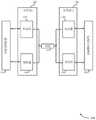
图5说明根据本发明的各种实施例的存储器装置500的实例。存储器装置500可为高带宽存储器(HBM)装置的实例。存储器装置500可经配置以针对存储器装置500中使用的每功率单位提供更多数据传送带宽。存储器装置500可包含存储器单元阵列505、处理器510及内插器515。存储器装置500可为参考图1描述的存储器装置100的实例。5 illustrates an example of a
存储器单元阵列505可为3D存储器阵列的实例。阵列505可包含多个存储器单元层叠520,每一层叠520是2D存储器阵列的实例。存储器单元阵列505还可包含耦合阵列505与内插器515的基底525。可使用一或多个穿硅通孔(TSV)(未展示)耦合存储器单元层叠520与基底525。存储器单元阵列505可为参考图1描述的存储器单元阵列105的实例。存储器单元阵列505可为DRAM技术、FeRAM技术或PCM技术的实例。
基底525可经配置为存储器单元阵列505的输入/输出(I/O)装置。在一些情况中,基底525可经配置为存储器单元阵列505的存储器控制器,其使用行解码器、列解码器、字线、数字线、其它组件或其组合存取各种存储器单元。在一些情况中,基底525可经配置以缓冲传达到存储器单元阵列505及从存储器单元阵列505传达的数据。基底525可包含信令接口(例如参考图1描述的信令接口120)以使用二进制信令及/或多电平信令跨内插器515传达数据。
处理器510可经配置以执行主机装置所要求的任何功能。在一些情况中,处理器510可为图形装置中的图形处理单元(GPU)的实例。在一些情况中,处理器510可为中央处理单元(CPU)的实例。在一些情况中,处理器510可包含存储器控制器(例如参考图1描述的控制器110)的功能性。处理器510可包含信令接口(例如参考图1描述的信令接口120)以使用二进制信令及/或多电平信令跨内插器515传达数据。处理器510及阵列505可使用微柱540与内插器耦合。The
内插器515经配置以提供所连接组件(例如,阵列505、处理器510及/或封装衬底535)之间的宽通信信道。内插器515可包含用于在装置之间通信的多个高电阻信道530。在一些情况中,信道530可完全彼此独立。一些信道530可为单向的且一些信道530可为双向的。阵列505及/或处理器510可选择信道的不同组合或群组以传达数据。
内插器515可通过提供大量信道530以连接组件而提供宽通信信道。在一些情况中,信道530可为连接器的薄迹线,借此使每一个别信道有损耗。由于每一信道530是电阻式的,所以随着传送数据的频率增加,传送数据所需的功率相对于频率以非线性方式增加。此类特性可带来实际频率上限,其可用于通过信道530在给定发射功率量的情况下发射数据。为增加在给定时间量中传送的数据量,内插器515可包含非常高数目个信道530。因而,存储器装置500的总线可宽于其它DRAM存储器,例如DDR4(双倍数据速率第四代同步动态随机存取存储器)或GDDR5(双倍数据速率型第五代同步图形随机存取存储器)。在一些情况中,存储器单元阵列505可具有每层叠520两个128位信道。因此,如果阵列505具有四个层叠520,那么处理器510将具有拥有4096个位的宽度的存储器总线。相比来说,一些GDDR存储器可仅具有拥有512个位的总宽度的存储器总线的十六个32位信道。内插器515可由与形成封装衬底535的第二材料不同的第一材料(例如,硅)形成。内插器515及封装衬底可使用一或多个焊料球545、550与其它组件耦合。
多电平信令(例如,PAM4)可与存储器装置500(例如,HBM装置)结合使用以增加数据传送速度而不增加数据传送频率。随着跨内插器515传达的数据频率增加,发射数据所需的功率增加。这是归因于信道530的损耗性质。多电平信令可经配置以增加跨内插器515传达的数据的数据速率而不增加数据的频率及/或发射功率。Multilevel signaling (eg, PAM4) may be used in conjunction with memory device 500 (eg, HBM device) to increase data transfer speed without increasing data transfer frequency. As the frequency of data communicated across
存储器装置500可经配置以选择可基于情境使用的各种类型的信令。举例来说,在一些情境(例如,控制信令)中,存储器装置500可希望使用二进制信令(例如,NRZ信令),且在其它情境(例如,用户数据)中,存储器装置可希望使用多电平信令(例如,PAM4、PAM8等)。
存储器装置500的各种组件可包含能够使用二进制信令及/或多电平信令进行通信的信令接口。举例来说,处理器510及/或基底525可包含信令接口,例如参考图1描述的信令界面120。Various components of
存储器装置500可经配置以对阵列505执行数个存取操作(例如,读取操作或写入操作)。针对写入操作,处理器510可识别待写入到存储器单元阵列505的信息。处理器510可基于经识别信息使用信令接口(或信令接口的驱动器)产生使用具有至少三个电平的第一调制方案调制的多电平信号。多电平信号可表示经识别信息的一个以上位。处理器510可使用内插器515的多个信道530将多电平信号发射到存储器单元阵列505。The
基底525可使用信令接口(或信令接口的接收器)接收及解码多电平信号。基底525可确定所接收多电平信号的振幅。举例来说,基底525可使用一或多个比较器以比较所接收多电平信号与一或多个电压阈值。基于是否满足电压阈值,比较器可输出特定信号。基底525可(例如,使用解码器)基于比较器的输出确定由多电平信号的振幅表示的多个位。基底525可识别一或多个存储器单元以存储多个位。基底525可将多个位写入到阵列505的一或多个存储器单元。
针对读取操作,处理器510可识别其希望用于其操作中的一者的存储于阵列505上的一些信息。处理器510可将信号(例如,二进制电平信号或多电平信号)发射到阵列505以请求经识别信息。基底525可识别当前存储经识别信息的一或多个存储器单元。基底525可使用参考图1描述的程序从经识别的一或多个单元读出一或多个数据位。For read operations,
基底525可基于从存储器单元读取的一或多个数据位使用信令接口(或信令接口的驱动器)产生使用具有至少三个电平的第一调制方案调制的多电平信号。基底525可使用内插器515的多个信道530将多电平信号发射到处理器510。
处理器510可使用信令接口(或信令接口的接收器)接收及解码多电平信号。处理器510可确定所接收多电平信号的振幅。举例来说,处理器510可使用一或多个比较器以比较所接收多电平信号与一或多个电压阈值。基于是否满足电压阈值,比较器可输出特定信号。处理器510可(例如,使用解码器)基于比较器的输出确定由多电平信号的振幅表示的多个位。The
图6展示根据本发明的实施例的支持具有宽系统接口的存储器中的多电平信令的信令组件615的框图600。信令组件615可为参考图1描述的信令接口120的组件。6 shows a block diagram 600 of a
信令组件615及/或其各种子组件的至少一些可在硬件、由处理器执行的软件、固件或其任何组合中实施。如果在由处理器执行的软件中实施,那么信令组件615及/或其各种子组件的至少一些的功能可由以下者执行:通用处理器、数字信号处理器(DSP)、专用集成电路(ASIC)、现场可编程门阵列(FPGA)或其它可编程逻辑装置、离散门或晶体管逻辑、离散硬件组件或经设计以执行本发明中描述的功能的其任何组合。信令组件615及/或其各种子组件的至少一些可物理地定位于各种位置处,包含经分布使得由一或多个物理装置在不同物理位置处实施功能的部分。在一些实例中,信令组件615及/或其各种子组件的至少一些可为根据本发明的各种实施例的单独且相异组件。在其它实例中,信令组件615及/或其各种子组件的至少一些可与一或多个其它硬件组件组合,包含(但不限于)I/O组件、收发器、网络服务器、另一计算装置、本发明中描述的一或多个其它组件或根据本发明的各种实施例的其组合。At least some of signaling
信令组件615可包含偏压组件620、时序组件625、信息管理器630、多电平信号产生器635、单元管理器640及二进制信号产生器645。这些组件中的每一者可彼此直接通信或(例如,经由一或多个总线)间接通信。
信息管理器630可通过存储器装置的控制器识别待写入到存储器单元阵列的信息。The
多电平信号产生器635可:通过控制器产生使用具有表示经识别信息的一组位的至少三个电平的第一调制方案调制的多电平信号;通过控制器跨包含一组信道的内插器将多电平信号发射到存储器单元阵列;及通过存储器单元阵列确定多电平信号的振幅是否满足一或多个阈值。The
单元管理器640可通过存储器单元阵列基于多电平信号所满足的一或多个阈值的阈值数目识别由多电平信号表示的所述组位且通过存储器单元阵列将由多电平信号表示的所述组位写入到存储器单元阵列的一或多个存储器单元。
二进制信号产生器645可通过控制器跨内插器将二进制电平信号与多电平信号同时发射到存储器单元阵列。The
图7展示根据本发明的实施例的包含支持具有宽系统接口的存储器中的多电平信令的装置705的系统700的图。装置705可为如上文(例如,参考图1)描述的控制器110的组件的实例或包含控制器110的组件。装置705可包含用于双向语音及数据通信的组件,其包含用于发射及接收通信的组件,包含信令组件715、存储器单元720、基本输入/输出系统(BIOS)组件725、处理器730、I/O控制器735及外围组件740。这些组件可经由一或多个总线(例如,总线710)电子通信。7 shows a diagram of a
存储器单元720可存储如本文中描述的信息(即,呈逻辑状态的形式)。
BIOS组件725是包含操作为固件的BIOS的软件组件,其可初始化及运行各种硬件组件。BIOS组件725还可管理处理器与各种其它组件(例如,外围组件、输入/输控制组件等)之间的数据流。BIOS组件725可包含存储于只读存储器(ROM)、快闪存储器或任何其它非易失性存储器中的程序或软件。
处理器730可包含智能硬件装置(例如,通用处理器、DSP、中央处理单元(CPU)、微控制器、ASIC、FPGA、可编程逻辑裝置、离散门或晶体管逻辑组件、离散硬件组件或其任何组合)。在一些情况中,处理器730可经配置以使用存储器控制器操作存储器阵列。在其它情况中,存储器控制器可整合到处理器730中。处理器730可经配置以执行存储于存储器中的计算机可读指令以执行各种功能(例如,支持具有宽系统接口的存储器中的多电平信令的功能或任务)。The
I/O控制器735可管理装置705的输入信号及输出信号。I/O控制器735还可管理未整合到装置705中的接口设备。在一些情况中,I/O控制器735可表示到外部接口设备的物理连接或端口。在一些情况中,I/O控制器735可利用操作系统,例如

外围组件740可包含任何输入或输出装置或此类装置的接口。实例可包含磁盘控制器、声音控制器、图形控制器、以太网络控制器、调制解调器、通用串行总线(USB)控制器、串行或并行端口或外围卡槽(例如外围组件互连(PCI)或加速图形端口(AGP)槽)。
输入745可表示装置705外部的装置或信号,其提供输入到装置705或装置705的组件。此可包含用户接口或与其它装置或其它装置之间的接口。在一些情况中,输入745可由I/O控制器735管理,且可经由外围组件740与装置705交互。Input 745 may represent a device or signal external to
输出750还可表示装置705外部的装置或信号,其经配置以从装置705或装置705的组件中的任一者接收输出。输出750的实例可包含显示器、音频扬声器、印刷装置、另一处理器或印刷电路板等。在一些情况中,输出750可为经由外围组件740与装置705介接的外围元件。在一些情况中,输出750可由I/O控制器735管理。
装置705的组件可包含经设计以实行其功能的电路。此可包含经配置以实行本文中描述的功能的各种电路元件,举例来说,导电线、晶体管、电容器、电感器、电阻器、放大器或其它作用或非作用元件。装置705可为计算机、服务器、膝上型计算机、笔记本计算机、平板计算机、移动电话、穿戴式电子装置、个人电子装置或类似物。或装置705可为此装置的部分或方面。The components of
在一个实施例中,装置705或系统700可包含:存储器单元阵列;控制器,其经配置以控制对存储器单元阵列的存取;内插器,其可操作地耦合存储器单元阵列与控制器,内插器包含存储器单元阵列与控制器之间的多个信道;及接收器,其经配置以解码跨内插器的至少一个信道传达的使用具有至少三个电平的第一调制方案调制的多电平信号。In one embodiment,
上文描述的装置705或系统700的一些实例还可包含驱动器,其经配置以至少部分基于多个信息位产生跨内插器的至少一个信道发射的多电平信号。Some examples of the
在上文描述的装置705或系统700的一些实例中,驱动器可经配置以使用格雷编码或数据总线反转或两者编码数据。In some examples of the
在上文描述的装置705或系统700的一些实例中,接收器进一步包括多个比较器,每一比较器经配置以比较多电平信号与电压阈值。In some examples of the
在上文描述的装置705或系统700的一些实例中,接收器进一步包括解码器,其经配置以至少部分基于从多个比较器的一组比较器接收的信息确定由多电平信号表示的多个位。In some examples of the
上文描述的装置705或系统700的一些实例还可包含可由多电平信号的振幅表示的多个信息位。Some examples of the
在上文描述的装置705或系统700的一些实例中,可使用PAM方案用信息编码多电平信号。In some examples of the
在上文描述的装置705或系统700的一些实例中,控制器跨内插器的多个信道的子集将多电平信号发射到存储器单元阵列。In some examples of the
在上文描述的装置705或系统700的一些实例中,控制器使用内插器的单向信道发射多电平信号。In some examples of the
在上文描述的装置705或系统700的一些实例中,存储器单元阵列跨内插器的多个信道的子集将多电平信号发射到控制器。In some examples of the
上文描述的装置705或系统700的一些实例还可包含由第一材料形成的衬底,其中内插器可由不同于第一材料的第二材料形成。在上文描述的装置705或系统700的一些实例中,第二材料可为硅。Some examples of the
上文描述的装置705或系统700的一些实例还可包含堆叠于存储器单元阵列的顶部上的第二存储器单元阵列,其中第二存储器单元阵列可通过内插器与控制器可操作地耦合。Some examples of the
上文描述的装置705或系统700的一些实例还可包含与存储器单元阵列及内插器耦合的输入/输出装置,其中输入/输出装置可经配置以缓冲与存储器单元阵列通信的信息。Some examples of the
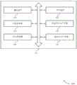
图8展示说明根据本发明的实施例的用于具有宽系统接口的存储器中的多电平信令的方法800的流程图。可通过如本文中描述的控制器110或其组件实施方法800的操作。举例来说,可通过如参考图7描述的信令组件执行方法800的操作。在一些实例中,控制器110可执行一组码来控制装置的功能元件以执行下文描述的功能。另外或替代地,控制器110可使用专用硬件来执行下文描述的功能的方面。8 shows a flowchart illustrating a
在一些情况中,所述方法还可包含通过存储器装置的控制器识别待写入到存储器单元阵列的信息。在一些情况中,所述方法还可包含通过控制器产生使用具有表示经识别信息的多个位的至少三个电平的第一调制方案调制的多电平信号。在一些情况中,所述方法还可包含通过控制器跨包含多个信道的内插器将多电平信号发射到存储器单元阵列。在一些情况中,所述方法还可包含通过存储器单元阵列确定多电平信号的振幅是否满足一或多个阈值。在一些情况中,所述方法还可包含通过存储器单元阵列至少部分基于多电平信号所满足的一或多个阈值的阈值数目识别由多电平信号表示的多个位。在一些情况中,所述方法还可包含通过存储器单元阵列将由多电平信号表示的多个位写入到存储器单元阵列的一或多个存储器单元。在一些情况中,所述方法还可包含通过控制器跨内插器将二进制电平信号与多电平信号同时发射到存储器单元阵列。In some cases, the method may also include identifying, by a controller of the memory device, information to be written to the array of memory cells. In some cases, the method may also include generating, by the controller, a multi-level signal modulated using the first modulation scheme having at least three levels representing the plurality of bits of the identified information. In some cases, the method may also include transmitting, by the controller, the multilevel signal to the array of memory cells across an interpolator that includes multiple channels. In some cases, the method may also include determining, by the array of memory cells, whether the amplitude of the multi-level signal satisfies one or more thresholds. In some cases, the method may also include identifying, by the memory cell array, a plurality of bits represented by the multi-level signal based at least in part on a threshold number of the one or more thresholds satisfied by the multi-level signal. In some cases, the method may also include writing, through the array of memory cells, a plurality of bits represented by the multi-level signal to one or more memory cells of the array of memory cells. In some cases, the method may also include simultaneously transmitting, by the controller, the binary-level signal and the multi-level signal to the array of memory cells across the interpolator.
在框805,控制器110可通过存储器装置的控制器识别待写入到存储器单元阵列的信息。可根据本文中描述的方法执行框805的操作。在特定实例中,可由如参考图7描述的信息管理器执行框805的操作的方面。At
在框810,控制器110可通过控制器产生使用具有表示经识别信息的多个位的至少三个电平的第一调制方案调制的多电平信号。可根据本文中描述的方法执行框810的操作。在特定实例中,可由如参考图7描述的多电平信号产生器执行框810的操作的方面。At
在框815,控制器110可通过控制器将多电平信号跨包含多个信道的内插器发射到存储器单元阵列。可根据本文中描述的方法执行框815的操作。在特定实例中,可由如参考图7描述的多电平信号产生器执行框815的操作的方面。At
描述一种方法。所述方法可包含:通过存储器装置的控制器识别待写入到存储器单元阵列的信息;通过控制器产生使用具有表示经识别信息的多个位的至少三个电平的第一调制方案调制的多电平信号;及通过控制器跨包含多个信道的内插器将多电平信号发射到存储器单元阵列。Describe a method. The method may include: identifying, by a controller of the memory device, information to be written to the array of memory cells; generating, by the controller, a signal modulated using a first modulation scheme having at least three levels of bits representing the identified information. a multi-level signal; and transmitting, by the controller, the multi-level signal to the array of memory cells across an interpolator comprising a plurality of channels.
方法800可由设备实施,所述设备可包含:用于通过存储器装置的控制器识别待写入到存储器单元阵列的信息的构件;用于通过控制器产生使用具有表示经识别信息的多个位的至少三个电平的第一调制方案调制的多电平信号的构件;及用于通过控制器跨包含多个信道的内插器将多电平信号发射到存储器单元阵列的构件。The
方法800可由另一设备实施,所述另一设备可包含:处理器;存储器,其与处理器电子通信;及指令,其存储于存储器中。指令可操作以导致处理器:通过存储器装置的控制器识别待写入到存储器单元阵列的信息;通过控制器产生使用具有表示经识别信息的多个位的至少三个电平的第一调制方案调制的多电平信号;及通过控制器跨包含多个信道的内插器将多电平信号发射到存储器单元阵列。
方法800可由可包含指令的非暂时性计算机可读媒体实施,所述指令可操作以导致处理器:通过存储器装置的控制器识别待写入到存储器单元阵列的信息;通过控制器产生使用具有表示经识别信息的多个位的至少三个电平的第一调制方案调制的多电平信号;及通过控制器跨包含多个信道的内插器将多电平信号发射到存储器单元阵列。
上文描述的方法800、设备及非暂时性计算机可读媒体的一些实例可进一步包含用于通过存储器单元阵列确定多电平信号的振幅是否满足一或多个阈值的过程、特征、构件或指令。Some examples of the
上文描述的方法800、设备及非暂时性计算机可读媒体的一些实例可进一步包含用于通过存储器单元阵列至少部分基于多电平信号可满足的一或多个阈值的阈值数目识别由多电平信号表示的多个位的过程、特征、构件或指令。Some examples of the
上文描述的方法800、设备及非暂时性计算机可读媒体的一些实例可进一步包含用于通过存储器单元阵列将由多电平信号表示的多个位写入到存储器单元阵列的一或多个存储器单元的过程、特征、构件或指令。Some examples of the
上文描述的方法800、设备及非暂时性计算机可读媒体的一些实例可进一步包含用于通过控制器跨内插器将二进制电平信号与多电平信号同时发射到存储器单元阵列的过程、特征、构件或指令。Some examples of the
在一个实施例中,装置或系统可包含:存储器单元阵列;内插器,其与存储器单元阵列可操作地耦合,所述内插器包含多个信道;控制器,其与内插器可操作地耦合,所述控制器经配置以:识别待写入到存储器单元阵列的信息;产生使用具有表示经识别信息的多个位的至少三个电平的第一调制方案调制的多电平信号;及跨内插器将多电平信号发射到存储器单元阵列。In one embodiment, a device or system can include: an array of memory cells; an interpolator operably coupled to the array of memory cells, the interpolator including a plurality of channels; a controller operative with the interpolator coupled to ground, the controller is configured to: identify information to be written to the memory cell array; generate a multilevel signal modulated using a first modulation scheme having at least three levels representing a plurality of bits of the identified information ; and transmitting a multi-level signal across the interpolator to the array of memory cells.
应注意,上文描述的方法描述可能实施方案,且操作及步骤可经重新布置或以其它方式修改使得其它实施方案是可能的。此外,可组合来自所述方法中的两者或两者以上的实施例。It should be noted that the methods described above describe possible implementations, and that operations and steps may be rearranged or otherwise modified such that other implementations are possible. Furthermore, two or more embodiments from the methods may be combined.
可使用各种不同科技及技术中的任一者来表示本文中描述的信息及信号。举例来说,可通过电压、电流、电磁波、磁场或磁性粒子、光场或光学粒子或其任何组合表示可贯穿上文描述参考的数据、指令、命令、信息、信号、位、符号及芯片。一些图式可将信号说明为单个信号;然而,所属领域的一般技术人员将理解,信号可表示信号总线,其中总线可具有各种位宽度。The information and signals described herein may be represented using any of a variety of different technologies and techniques. For example, the data, instructions, commands, information, signals, bits, symbols and chips that may be referenced throughout the above description may be represented by voltages, currents, electromagnetic waves, magnetic or magnetic particles, light fields or optical particles, or any combination thereof. Some drawings may illustrate a signal as a single signal; however, one of ordinary skill in the art will understand that a signal may represent a bus of signals, where the bus may have various bit widths.
如本文中使用,术语“虚拟接地”是指保持在约零伏特(0V)的电压但不与接地直接连接的电路的节点。因此,虚拟接地的电压可暂时波动且在稳定状态下返回到约0V。可使用各种电子电路元件(例如由运算放大器及电阻器构成的分压器)来实施虚拟接地。其它实施方案还是可能的。“虚拟接地”或“经虚拟接地”意味着连接到约0V。As used herein, the term "virtual ground" refers to a node of a circuit that is maintained at a voltage of about zero volts (0V) but is not directly connected to ground. Therefore, the voltage of the virtual ground may fluctuate temporarily and return to about 0V in a steady state. The virtual ground may be implemented using various electronic circuit elements, such as a voltage divider composed of operational amplifiers and resistors. Other implementations are also possible. "Virtual ground" or "via virtual ground" means connected to about 0V.
术语“电子通信”及“耦合”是指组件之间的关系,其支持组件之间的电子流。此可包含组件之间的直接连接或可包含中间组件。电子通信中的组件可为主动交换的电子或信号(例如,在通电电路中)或可并非主动交换的电子或信号(例如,在断电电路中),但可经配置且可操作以在使电路通电之后交换电子或信号。通过实例,经由开关(例如,晶体管)物理连接的两个组件电子通信,而不管开关的状态(即,断开或闭合)为何。The terms "electronic communication" and "coupling" refer to a relationship between components that supports the flow of electrons between the components. This may include direct connections between components or may include intermediate components. Components in electronic communication may be actively exchanged electrons or signals (eg, in an energized circuit) or may not be actively exchanged electrons or signals (eg, in a de-energized circuit), but may be configured and operable to enable A circuit exchanges electrons or signals after it is energized. By way of example, two components that are physically connected via a switch (eg, a transistor) communicate electronically regardless of the state of the switch (ie, open or closed).
如本文中使用,术语“大体上”意味着所修饰特性(例如,由术语大体上修饰的动词或形容词)无需是绝对的,但足够接近以便实现特性的优点。As used herein, the term "substantially" means that the property being modified (eg, a verb or adjective modified by the term substantially) need not be absolute, but close enough to achieve the benefit of the property.
如本文中使用,术语“电极”可指导电体,且在一些情况中可采用为到存储器阵列的存储器单元或其它组件的电接触。电极可包含提供存储器装置100的元件或组件之间的导电路径的迹线、线、导电线、导电层或类似物。As used herein, the term "electrode" may refer to an electrical conductor, and in some cases may be employed as an electrical contact to memory cells or other components of a memory array. Electrodes may include traces, wires, conductive lines, conductive layers, or the like that provide conductive paths between elements or components of
如本文中使用,术语“光刻”可指使用光致抗蚀剂材料进行图案化且使用电磁辐射暴露此类材料的工艺。举例来说,可通过例如将光致抗蚀剂旋涂于基底材料上而将光致抗蚀剂材料形成于基底材料上。可通过将光致抗蚀剂暴露到辐射而在光致抗蚀剂中产生图案。举例来说,可通过在空间上描绘辐射暴露光致抗蚀剂的位置的光掩模界定图案。举例来说,接着可通过化学处理移除所暴露光致抗蚀剂区域,从而留下所要图案。在一些情况中,可保持暴露区且可移除未暴露区。As used herein, the term "lithography" may refer to a process of patterning using photoresist materials and exposing such materials using electromagnetic radiation. For example, the photoresist material can be formed on the base material by, for example, spin coating the photoresist on the base material. Patterns can be created in the photoresist by exposing the photoresist to radiation. For example, the pattern can be defined by a photomask that spatially delineates where the radiation exposes the photoresist. For example, the exposed photoresist areas may then be removed by chemical processing, leaving the desired pattern. In some cases, exposed areas may remain and unexposed areas may be removed.
硫属化物材料可为包含元素S、Se及Te中的至少一者的材料或合金。本文中论述的相变材料可为硫属化物材料。硫属化物材料可包含S、Se、Te、Ge、As、Al、Sb、Au、铟(In)、镓(Ga)、锡(Sn)、铋(Bi)、钯(Pd)、钴(Co)、氧(O)、银(Ag)、镍(Ni)、铂(Pt)的合金。实例硫属化物材料及合金可包含但不限于Ge-Te、In-Se、Sb-Te、Ga-Sb、In-Sb、As-Te、Al-Te、Ge-Sb-Te、Te-Ge-As、In-Sb-Te、Te-Sn-Se、Ge-Se-Ga、Bi-Se-Sb、Ga-Se-Te、Sn-Sb-Te、In-Sb-Ge、Te-Ge-Sb-S、Te-Ge-Sn-O、Te-Ge-Sn-Au、Pd-Te-Ge-Sn、In-Se-Ti-Co、Ge-Sb-Te-Pd、Ge-Sb-Te-Co、Sb-Te-Bi-Se、Ag-In-Sb-Te、Ge-Sb-Se-Te、Ge-Sn-Sb-Te、Ge-Te-Sn-Ni、Ge-Te-Sn-Pd或Ge-Te-Sn-Pt。如本文中使用,用连字符连接的化学组合物标记指示包含于特定化合物或合金中的元素且希望表示涉及所指示元素的所有理想配比。举例来说,Ge-Te可包含GexTey,其中x及y可为任何正整数。可变电阻材料的其它实例可包含二元金属氧化物材料或包含两种或两种以上金属(例如,转变金属、碱土金属及/或稀土金属)的混价氧化物。实施例不限于与存储器单元的存储器元件相关联的一或若干特定可变电阻材料。举例来说,可变电阻材料的其它实例可用于形成存储器元件且可包含硫属化物材料、巨磁阻材料或基于聚合物的材料等。The chalcogenide material may be a material or alloy that includes at least one of the elements S, Se, and Te. The phase change materials discussed herein may be chalcogenide materials. The chalcogenide material may include S, Se, Te, Ge, As, Al, Sb, Au, Indium (In), Gallium (Ga), Tin (Sn), Bismuth (Bi), Palladium (Pd), Cobalt (Co) ), oxygen (O), silver (Ag), nickel (Ni), platinum (Pt) alloy. Example chalcogenide materials and alloys may include, but are not limited to, Ge-Te, In-Se, Sb-Te, Ga-Sb, In-Sb, As-Te, Al-Te, Ge-Sb-Te, Te-Ge- As, In-Sb-Te, Te-Sn-Se, Ge-Se-Ga, Bi-Se-Sb, Ga-Se-Te, Sn-Sb-Te, In-Sb-Ge, Te-Ge-Sb- S, Te-Ge-Sn-O, Te-Ge-Sn-Au, Pd-Te-Ge-Sn, In-Se-Ti-Co, Ge-Sb-Te-Pd, Ge-Sb-Te-Co, Sb-Te-Bi-Se, Ag-In-Sb-Te, Ge-Sb-Se-Te, Ge-Sn-Sb-Te, Ge-Te-Sn-Ni, Ge-Te-Sn-Pd or Ge- Te-Sn-Pt. As used herein, a hyphenated chemical composition designation indicates an element contained in a particular compound or alloy and is intended to represent all stoichiometric ratios involving the indicated element. For example, Ge-Te can include GexTey, wherex andy can be any positive integers. Other examples of variable resistance materials may include binary metal oxide materials or mixed oxides including two or more metals (eg, transition metals, alkaline earth metals, and/or rare earth metals). Embodiments are not limited to one or several specific variable resistance materials associated with the memory elements of the memory cells. For example, other examples of variable resistance materials can be used to form memory elements and can include chalcogenide materials, giant magnetoresistive materials, or polymer-based materials, among others.
术语“隔离”是指组件之间的关系,其中电子当前无法在其之间流动;如果组件之间存在开路,那么其彼此隔离。举例来说,通过开关物理连接的两个组件可在开关断开时彼此隔离。The term "isolation" refers to the relationship between components in which electrons cannot currently flow between them; if there is an open circuit between the components, they are isolated from each other. For example, two components physically connected by a switch can be isolated from each other when the switch is open.
如本文使用,术语“短接”是指组件之间的关系,其中经由所述两个组件之间的单个中间组件的激活而在组件之间建立导电路径。举例来说,短接到第二组件的第一组件可在两个组件之间的开关闭合时与第二组件交换电子。因此,短接可为动态操作,其实现电子通信的组件(或线)之间的电荷的流动。As used herein, the term "shorting" refers to a relationship between components wherein a conductive path is established between the components via activation of a single intermediate component between the two components. For example, a first component shorted to a second component can exchange electrons with the second component when the switch between the two components is closed. Thus, shorting can be a dynamic operation that enables the flow of charge between components (or wires) of electronic communication.
本文中论述的装置(包含存储器装置100)可形成于半导体衬底(例如硅、锗、硅锗合金、砷化镓、氮化镓等)上。在一些情况中,衬底是半导体晶片。在其它情况中,衬底可为绝缘体上硅(SOI)衬底(例如玻璃上硅(SOG)或蓝宝石上硅(SOP))或另一衬底上的半导体材料的外延层。可通过使用各种化学物种(包含但不限于磷、硼或砷)掺杂来控制衬底或衬底的子区的导电率。可通过离子植入或通过任何其它掺杂方法在衬底的初始形成或生长期间执行掺杂。The devices discussed herein, including the
本文中论述的晶体管可表示场效应晶体管(FET)且包括包含源极、漏极与栅极的三终端装置。所述终端可通过导电材料(例如,金属)连接到其它电子元件。源极及漏极可为导电的且可包括重度掺杂(例如,简并)半导体区。可通过轻度掺杂半导体区或沟道分离源极及漏极。如果沟道是n型(即,多数载子是电子),那么FET可称为n型FET。如果沟道是p型(即,多数载子是空穴),那么FET可称为p型FET。沟道可通过绝缘栅极氧化物封端。可通过施加电压到栅极而控制沟道导电率。举例来说,分别施加正电压或负电压到n型FET或p型FET可导致沟道变成导电的。当施加大于或等于晶体管的阈值电压的电压到晶体管栅极时,可“开启”或“激活”所述晶体管。当施加小于晶体管的阈值电压的电压到晶体管栅极时,可“关闭”或“撤销激活”所述晶体管。The transistors discussed herein may represent field effect transistors (FETs) and include three terminal devices including a source, a drain, and a gate. The terminals may be connected to other electronic components through conductive material (eg, metal). The source and drain electrodes may be conductive and may include heavily doped (eg, degenerate) semiconductor regions. The source and drain can be separated by lightly doped semiconductor regions or channels. If the channel is n-type (ie, the majority carriers are electrons), then the FET can be referred to as an n-type FET. If the channel is p-type (ie, the majority carriers are holes), then the FET can be referred to as a p-type FET. The channel can be terminated by an insulating gate oxide. Channel conductivity can be controlled by applying a voltage to the gate. For example, applying a positive or negative voltage to an n-type FET or p-type FET, respectively, can cause the channel to become conductive. A transistor may be "turned on" or "activated" when a voltage greater than or equal to the transistor's threshold voltage is applied to the gate of the transistor. A transistor may be "turned off" or "deactivated" when a voltage less than the transistor's threshold voltage is applied to the gate of the transistor.
本文中陈述的描述以及附图描述实例配置且不表示可实施或在权利要求书的范围内的所有实例。本文中使用的术语“实例”意味着“充当实例、例子或图解”且非“优选”或“优于其它实例”。实施方式出于提供对所描述技术的理解的目的而包含具体细节。然而,可在不无这些具体细节的情况下实践这些技术。在一些例子中,以框图形式展示众所周知结构及装置以避免模糊所描述实例的概念。The descriptions set forth herein and the drawings describe example configurations and do not represent all examples that may be implemented or within the scope of the claims. The term "example" as used herein means "serving as an example, instance, or illustration" and not "preferred" or "preferred over other examples." The embodiments contain specific details for the purpose of providing an understanding of the described techniques. However, these techniques may be practiced without these specific details. In some instances, well-known structures and devices are shown in block diagram form in order to avoid obscuring the concepts of the described examples.
在附图中,类似组件或特征可具有相同参考标签。此外,可通过在参考标签后加破折号及区分类似组件的第二标签来区分相同类型的各种组件。当仅在说明书中使用第一参考标签时,描述可适用于具有相同第一参考标签的类似组件中的任一者,而与第二参考标签无关。In the drawings, similar components or features may have the same reference labels. Additionally, various components of the same type may be distinguished by following the reference label with a dash and a second label that distinguishes similar components. When only a first reference label is used in the specification, the description may apply to any of the similar components having the same first reference label, regardless of the second reference label.
可使用各种不同科技及技术中的任一者来表示本文描述的信息及信号。举例来说,可通过电压、电流、电磁波、磁场或磁性粒子、光场或光学粒子或其任何组合表示可贯穿上文描述引用的数据、指令、命令、信息、信号、位、符号及芯片。The information and signals described herein may be represented using any of a variety of different technologies and techniques. For example, the data, instructions, commands, information, signals, bits, symbols, and chips that may be referenced throughout the above description may be represented by voltages, currents, electromagnetic waves, magnetic or magnetic particles, light fields or optical particles, or any combination thereof.
可使用经设计以执行本文中描述的功能的通用处理器、DSP、ASIC、FPGA或其它可编程逻辑装置、离散门或晶体管逻辑、离散硬件组件或其任何组合而实施或执行结合本文的揭示内容描述的各种说明性框及组件。通用处理器可为微处理器,但在替代例中,处理器可为任何常规处理器、控制器、微控制器或状态机。处理器还可实施为计算装置的组合(例如,数字信号处理器(DSP)及微处理器的组合、多个微处理器、结合DSP核心的一或多个微处理器或任何其它此配置)。The disclosures incorporated herein may be implemented or carried out using general purpose processors, DSPs, ASICs, FPGAs or other programmable logic devices, discrete gate or transistor logic, discrete hardware components, or any combination thereof designed to perform the functions described herein Various illustrative blocks and components are described. A general-purpose processor may be a microprocessor, but in the alternative, the processor may be any conventional processor, controller, microcontroller, or state machine. A processor may also be implemented as a combination of computing devices (eg, a combination of a digital signal processor (DSP) and a microprocessor, multiple microprocessors, one or more microprocessors combined with a DSP core, or any other such configuration) .
可在硬件、由处理器执行的软件、固件或其任何组合中实施本文中描述的功能。如果在由处理器执行的软件中实施,那么可将功能作为一或多个指令或码存储于计算机可读媒体上或经由计算机可读媒体发射。其它实例及实施方案是在本发明及所附权利要求书的范围内。举例来说,归因于软件的性质,可使用由处理器执行的软件、硬件、固件、硬接线或这些中的任意者的组合来实施上文描述的功能。实施功能的特征还可物理上定位在各种位置处,包含经分布使得在不同物理位置处实施功能的部分。而且,如本文中所使用,包含在权利要求书中,如物项列表(例如,以例如“中的至少一者”或“中的一或多者”的短语开始的物项列表)中使用的“或”指示包含列表,使得(例如)A、B或C中的至少一者的列表意指A或B或C或AB或AC或BC或ABC(即,A及B及C)。而且,如本文中使用,短语“基于”不应解释为对条件闭集的参考。举例来说,在不脱离本发明的范围的情况下,描述为“基于条件A”的实例步骤可基于条件A及条件B两者。换句话说,如本文中使用,短语“基于”应按与短语“至少部分基于”相同的方式来解释。The functions described herein may be implemented in hardware, software executed by a processor, firmware, or any combination thereof. If implemented in software executed by a processor, the functions may be stored on or transmitted over as one or more instructions or code on a computer-readable medium. Other examples and implementations are within the scope of the invention and the appended claims. For example, due to the nature of software, the functions described above may be implemented using software executed by a processor, hardware, firmware, hardwiring, or a combination of any of these. Features that implement functions may also be physically located at various locations, including portions that are distributed such that functions are implemented at different physical locations. Also, as used herein, included in the claims, as used in a list of items (eg, a list of items beginning with a phrase such as "at least one of" or "one or more of") The "or" of ' indicates that a list is included such that, for example, a list of at least one of A, B, or C means A or B or C or AB or AC or BC or ABC (ie, A and B and C). Also, as used herein, the phrase "based on" should not be construed as a reference to a closed set of conditions. For example, an example step described as "based on condition A" may be based on both condition A and condition B without departing from the scope of this disclosure. In other words, as used herein, the phrase "based on" should be construed in the same manner as the phrase "based at least in part on."
计算机可读媒体包含非暂时性计算机存储媒体及通信媒体两者,包含促进计算机程序从一个位置传送到另一位置的任何媒体。非暂时性存储媒体可为可通过通用或专用计算机存取的任何可用媒体。通过实例但非限制,非暂时性计算机可读媒体可包括RAM、ROM、电可擦除可编程只读存储器(EEPROM)、光盘(CD)ROM或其它光盘存储器、磁盘存储器或其它磁性存储装置或可用于携载或存储呈指令或数据结构形式的所要程序代码构件且可通过通用或专用计算机或通用或专用处理器存取的任何其它非暂时性媒体。而且,任何连接适当地称为计算机可读媒体。举例来说,如果使用同轴电缆、光纤电缆、双绞线、数字用户线(DSL)或例如红外线、无线电及微波的无线科技从网站、服务器或其它远程源发射软件,那么同轴电缆、光纤电缆、双绞线、数字用户线(DSL)或例如红外线、无线电及微波的无线科技包含于媒体的定义中。如本文中使用,磁盘及光盘包含CD、激光光盘、光盘、数字多功能光盘(DVD)、软磁盘及蓝光光盘,其中磁盘通常磁性地再现数据,而光盘使用激光光学地再现数据。上文的组合还包含于计算机可读媒体的范围内。Computer-readable media includes both non-transitory computer storage media and communication media including any medium that facilitates transfer of a computer program from one place to another. Non-transitory storage media can be any available media that can be accessed by a general purpose or special purpose computer. By way of example and not limitation, non-transitory computer readable media may include RAM, ROM, electrically erasable programmable read only memory (EEPROM), compact disk (CD) ROM or other optical disk storage, magnetic disk storage or other magnetic storage or Any other non-transitory medium that can be used to carry or store the desired program code means in the form of instructions or data structures and which can be accessed by a general purpose or special purpose computer or general purpose or special purpose processor. Also, any connection is properly termed a computer-readable medium. For example, if coaxial cable, fiber optic cable, twisted pair, digital subscriber line (DSL), or wireless technologies such as infrared, radio, and microwave are used to transmit software from a website, server, or other remote source, coaxial cable, fiber optic cable, or Cable, twisted pair, digital subscriber line (DSL) or wireless technologies such as infrared, radio and microwave are included in the definition of media. Disk and disc, as used herein, includes CD, laser disc, optical disc, digital versatile disc (DVD), floppy disk, and blu-ray disc, where disks typically reproduce data magnetically, while discs reproduce data optically using lasers. Combinations of the above are also included within the scope of computer-readable media.
提供本文中的描述以使所属领域的技术人员能够制成或使用本发明。所属领域的技术人员将容易明白本发明的各种修改,且本文中定义的通用原理可应用于其它变化而不背离本发明的范围。因此,本发明不限于本文中描述的实例及设计,而应符合与本文中揭示的原则及新颖特征一致的最广范围。The description herein is provided to enable any person skilled in the art to make or use the present invention. Various modifications to this invention will be readily apparent to those skilled in the art, and the generic principles defined herein may be applied to other variations without departing from the scope of this invention. Thus, the present disclosure is not limited to the examples and designs described herein but is to be accorded the widest scope consistent with the principles and novel features disclosed herein.
Claims (21)
Translated fromChinesePriority Applications (1)
| Application Number | Priority Date | Filing Date | Title |
|---|---|---|---|
| CN202411526233.5ACN119446223A (en) | 2017-08-07 | 2018-07-23 | Multi-level signaling in memories with wide system interfaces |
Applications Claiming Priority (5)
| Application Number | Priority Date | Filing Date | Title |
|---|---|---|---|
| US201762542160P | 2017-08-07 | 2017-08-07 | |
| US62/542,160 | 2017-08-07 | ||
| US15/854,600 | 2017-12-26 | ||
| US15/854,600US10425260B2 (en) | 2017-08-07 | 2017-12-26 | Multi-level signaling in memory with wide system interface |
| PCT/US2018/043311WO2019032271A1 (en) | 2017-08-07 | 2018-07-23 | Multi-level signaling in memory with wide system interface |
Related Child Applications (1)
| Application Number | Title | Priority Date | Filing Date |
|---|---|---|---|
| CN202411526233.5ADivisionCN119446223A (en) | 2017-08-07 | 2018-07-23 | Multi-level signaling in memories with wide system interfaces |
Publications (1)
| Publication Number | Publication Date |
|---|---|
| CN110870013Atrue CN110870013A (en) | 2020-03-06 |
Family
ID=65231167
Family Applications (2)
| Application Number | Title | Priority Date | Filing Date |
|---|---|---|---|
| CN202411526233.5APendingCN119446223A (en) | 2017-08-07 | 2018-07-23 | Multi-level signaling in memories with wide system interfaces |
| CN201880045340.2APendingCN110870013A (en) | 2017-08-07 | 2018-07-23 | Multilevel signaling in memory with wide system interface |
Family Applications Before (1)
| Application Number | Title | Priority Date | Filing Date |
|---|---|---|---|
| CN202411526233.5APendingCN119446223A (en) | 2017-08-07 | 2018-07-23 | Multi-level signaling in memories with wide system interfaces |
Country Status (6)
| Country | Link |
|---|---|
| US (5) | US10425260B2 (en) |
| EP (1) | EP3665684A4 (en) |
| KR (2) | KR20210108495A (en) |
| CN (2) | CN119446223A (en) |
| TW (4) | TWI740553B (en) |
| WO (1) | WO2019032271A1 (en) |
Cited By (3)
| Publication number | Priority date | Publication date | Assignee | Title |
|---|---|---|---|---|
| CN111459864A (en)* | 2020-04-02 | 2020-07-28 | 深圳朗田亩半导体科技有限公司 | Memory device and manufacturing method thereof |
| CN114846550A (en)* | 2019-12-20 | 2022-08-02 | 美光科技公司 | Multipurpose Signaling for Memory Systems |
| CN116368471A (en)* | 2020-06-22 | 2023-06-30 | 美光科技公司 | Reading algorithm for memory device |
Families Citing this family (52)
| Publication number | Priority date | Publication date | Assignee | Title |
|---|---|---|---|---|
| US10365833B2 (en)* | 2016-01-22 | 2019-07-30 | Micron Technology, Inc. | Apparatuses and methods for encoding and decoding of signal lines for multi-level communication architectures |
| US10283187B2 (en) | 2017-07-19 | 2019-05-07 | Micron Technology, Inc. | Apparatuses and methods for providing additional drive to multilevel signals representing data |
| US10447512B2 (en) | 2017-08-07 | 2019-10-15 | Micron Technology, Inc. | Channel equalization for multi-level signaling |
| US10425260B2 (en) | 2017-08-07 | 2019-09-24 | Micron Technology, Inc. | Multi-level signaling in memory with wide system interface |
| US10277435B2 (en) | 2017-08-07 | 2019-04-30 | Micron Technology, Inc. | Method to vertically align multi-level cells |
| US10403337B2 (en) | 2017-08-07 | 2019-09-03 | Micron Technology, Inc. | Output driver for multi-level signaling |
| US10530617B2 (en) | 2017-08-07 | 2020-01-07 | Micron Technology, Inc. | Programmable channel equalization for multi-level signaling |
| US10277441B2 (en) | 2017-08-07 | 2019-04-30 | Micron Technology, Inc. | Uniformity between levels of a multi-level signal |
| US10128842B1 (en)* | 2018-03-23 | 2018-11-13 | Micron Technology, Inc. | Output impedance calibration for signaling |
| KR102401996B1 (en)* | 2018-05-28 | 2022-05-24 | 삼성전자주식회사 | Semiconductor device including a high-speed receiver being capable of adjusting timing skew for multi-level signal and testing equipment including the receiver |
| US11152333B2 (en)* | 2018-10-19 | 2021-10-19 | Micron Technology, Inc. | Semiconductor device packages with enhanced heat management and related systems |
| US10811402B2 (en) | 2018-12-26 | 2020-10-20 | AP Memory Technology Corp. | Memory device and microelectronic package having the same |
| US11158552B2 (en) | 2018-12-26 | 2021-10-26 | AP Memory Technology Corp. | Semiconductor device and method to manufacture the same |
| US11380614B2 (en) | 2018-12-26 | 2022-07-05 | AP Memory Technology Corp. | Circuit assembly |
| US11672111B2 (en) | 2018-12-26 | 2023-06-06 | Ap Memory Technology Corporation | Semiconductor structure and method for manufacturing a plurality thereof |
| US11417628B2 (en) | 2018-12-26 | 2022-08-16 | Ap Memory Technology Corporation | Method for manufacturing semiconductor structure |
| US11194726B2 (en)* | 2019-02-25 | 2021-12-07 | Micron Technology, Inc. | Stacked memory dice for combined access operations |
| US11855056B1 (en)* | 2019-03-15 | 2023-12-26 | Eliyan Corporation | Low cost solution for 2.5D and 3D packaging using USR chiplets |
| US11609865B2 (en)* | 2019-04-17 | 2023-03-21 | Micron Technology, Inc. | Method and apparatus for signal path biasing in a memory system |
| EP4567810A3 (en)* | 2019-05-30 | 2025-09-17 | Micron Technology, Inc. | Apparatuses and methods including multilevel command and address signals |
| CN112712832B (en)* | 2019-10-25 | 2024-09-20 | 长鑫存储技术(上海)有限公司 | Write operation circuit, semiconductor memory and write operation method |
| US11870616B2 (en) | 2020-01-27 | 2024-01-09 | Micron Technology, Inc. | Postamble for multi-level signal modulation |
| KR102266069B1 (en)* | 2020-07-09 | 2021-06-18 | 고려대학교 산학협력단 | Wireline transceiver based on pulse amplitude modulation-4 |
| US11239169B1 (en) | 2020-07-24 | 2022-02-01 | Micron Technology, Inc. | Semiconductor memory stacks connected to processing units and associated systems and methods |
| KR20220031791A (en) | 2020-09-03 | 2022-03-14 | 삼성전자주식회사 | Memory device, operating method of the same, and memory system |
| KR20220050316A (en) | 2020-10-16 | 2022-04-25 | 삼성전자주식회사 | Multi-level signal generator for test and memory device including the same |
| KR20220050683A (en) | 2020-10-16 | 2022-04-25 | 삼성전자주식회사 | Memory device supporting high-efficiency i/o interface and memory system including the same |
| KR20220079195A (en) | 2020-12-04 | 2022-06-13 | 삼성전자주식회사 | Test Device, Test System and Operating Method of Test System |
| US12021668B2 (en)* | 2020-12-28 | 2024-06-25 | Micron Technology, Inc. | Equalization for pulse-amplitude modulation |
| US11551730B2 (en) | 2021-01-26 | 2023-01-10 | Qualcomm Incorporated | Low power memory system using dual input-output voltage supplies |
| KR20220108265A (en) | 2021-01-26 | 2022-08-03 | 삼성전자주식회사 | High bandwidth memory system using multi-level signaling |
| JP7200273B2 (en)* | 2021-01-28 | 2023-01-06 | アンリツ株式会社 | ERROR DETECTION DEVICE AND ERROR DETECTION METHOD |
| US12087393B2 (en)* | 2021-04-29 | 2024-09-10 | Micron Technology, Inc. | Multi-driver signaling |
| US12438095B1 (en) | 2021-05-06 | 2025-10-07 | Eliyan Corp. | Complex system-in-package architectures leveraging high-bandwidth long-reach die-to-die connectivity over package substrates |
| US11855043B1 (en) | 2021-05-06 | 2023-12-26 | Eliyan Corporation | Complex system-in-package architectures leveraging high-bandwidth long-reach die-to-die connectivity over package substrates |
| US12204794B1 (en) | 2021-05-18 | 2025-01-21 | Eliyan Corporation | Architecture for DRAM control optimization using simultaneous bidirectional memory interfaces |
| KR102860132B1 (en) | 2021-06-18 | 2025-09-15 | 삼성전자주식회사 | Memory device and semiconductor device including the same |
| US12154656B2 (en)* | 2021-11-11 | 2024-11-26 | Advanced Micro Devices, Inc. | Error pin training with graphics DDR memory |
| US12190038B1 (en) | 2021-11-25 | 2025-01-07 | Eliyan Corporation | Multi-chip module (MCM) with multi-port unified memory |
| US11842986B1 (en) | 2021-11-25 | 2023-12-12 | Eliyan Corporation | Multi-chip module (MCM) with interface adapter circuitry |
| US12002541B2 (en)* | 2021-12-08 | 2024-06-04 | Advanced Micro Devices, Inc. | Read clock toggle at configurable PAM levels |
| US12394467B2 (en) | 2021-12-08 | 2025-08-19 | Advanced Micro Devices, Inc. | Read clock start and stop for synchronous memories |
| US11841815B1 (en) | 2021-12-31 | 2023-12-12 | Eliyan Corporation | Chiplet gearbox for low-cost multi-chip module applications |
| WO2023165729A1 (en) | 2022-03-01 | 2023-09-07 | Graphcore Limited | Dram module with data routing logic |
| US12248419B1 (en) | 2022-05-26 | 2025-03-11 | Eliyan Corporation | Interface conversion circuitry for universal chiplet interconnect express (UCIe) |
| US11803437B1 (en) | 2022-06-30 | 2023-10-31 | Advanced Micro Devices, Inc. | Write hardware training acceleration |
| US12093202B2 (en) | 2022-12-12 | 2024-09-17 | Global Unichip Corporation | DBI encoding device and DBI encoding method |
| US12058874B1 (en) | 2022-12-27 | 2024-08-06 | Eliyan Corporation | Universal network-attached memory architecture |
| US12182040B1 (en) | 2023-06-05 | 2024-12-31 | Eliyan Corporation | Multi-chip module (MCM) with scalable high bandwidth memory |
| US12436556B2 (en)* | 2023-09-15 | 2025-10-07 | Nxp B.V. | Communication protocol for die to die interface |
| US12204482B1 (en) | 2023-10-09 | 2025-01-21 | Eliyan Corporation | Memory chiplet with efficient mapping of memory-centric interface to die-to-die (D2D) unit interface modules |
| US12248413B1 (en) | 2023-10-11 | 2025-03-11 | Eliyan Corporation | Universal memory interface utilizing die-to-die (D2D) interfaces between chiplets |
Citations (2)
| Publication number | Priority date | Publication date | Assignee | Title |
|---|---|---|---|---|
| CN103391092A (en)* | 2013-03-01 | 2013-11-13 | 友达光电股份有限公司 | Method for Multilevel Data Transmission |
| US20170133103A1 (en)* | 2015-11-05 | 2017-05-11 | SK Hynix Inc. | Stack type semiconductor memory and semiconductor system using the same |
Family Cites Families (151)
| Publication number | Priority date | Publication date | Assignee | Title |
|---|---|---|---|---|
| US8604828B1 (en) | 1996-05-31 | 2013-12-10 | International Business Machines Corporation | Variable voltage CMOS off-chip driver and receiver circuits |
| US5757242A (en) | 1996-12-09 | 1998-05-26 | Industrial Technology Research Institute | Low power consumption oscillators with output level shifters |
| US6294937B1 (en) | 1999-05-25 | 2001-09-25 | Lsi Logic Corporation | Method and apparatus for self correcting parallel I/O circuitry |
| JP2001024495A (en) | 1999-07-05 | 2001-01-26 | Mitsubishi Electric Corp | Output buffer circuit |
| US7269212B1 (en) | 2000-09-05 | 2007-09-11 | Rambus Inc. | Low-latency equalization in multi-level, multi-line communication systems |
| US7124221B1 (en)* | 1999-10-19 | 2006-10-17 | Rambus Inc. | Low latency multi-level communication interface |
| US6396329B1 (en) | 1999-10-19 | 2002-05-28 | Rambus, Inc | Method and apparatus for receiving high speed signals with low latency |
| US7072415B2 (en) | 1999-10-19 | 2006-07-04 | Rambus Inc. | Method and apparatus for generating multi-level reference voltage in systems using equalization or crosstalk cancellation |
| US6574758B1 (en) | 2000-03-10 | 2003-06-03 | Cisco Technology, Inc. | Testing a bus coupled between two electronic devices |
| KR100381962B1 (en) | 2000-08-07 | 2003-05-01 | 삼성전자주식회사 | Row decoder of nonvolatile memory device |
| US6993107B2 (en) | 2001-01-16 | 2006-01-31 | International Business Machines Corporation | Analog unidirectional serial link architecture |
| US6507225B2 (en) | 2001-04-16 | 2003-01-14 | Intel Corporation | Current mode driver with variable equalization |
| US6636821B2 (en) | 2001-07-03 | 2003-10-21 | International Business Machines Corporation | Output driver impedance calibration circuit |
| US20030070126A1 (en) | 2001-09-14 | 2003-04-10 | Werner Carl W. | Built-in self-testing of multilevel signal interfaces |
| KR100866867B1 (en) | 2002-02-27 | 2008-11-04 | 주식회사 엘지이아이 | Timing restoration device |
| US7167527B1 (en)* | 2002-05-02 | 2007-01-23 | Integrated Memory Logic, Inc. | System and method for multi-symbol interfacing |
| KR100482405B1 (en)* | 2002-11-01 | 2005-04-14 | 삼성전자주식회사 | Semiconductor memory device having hierachical data input/output line and method for precharging therefor |
| US7126378B2 (en) | 2003-12-17 | 2006-10-24 | Rambus, Inc. | High speed signaling system with adaptive transmit pre-emphasis |
| DE10319271A1 (en)* | 2003-04-29 | 2004-11-25 | Infineon Technologies Ag | Memory circuitry and manufacturing method |
| US6894529B1 (en) | 2003-07-09 | 2005-05-17 | Integrated Device Technology, Inc. | Impedance-matched output driver circuits having linear characteristics and enhanced coarse and fine tuning control |
| US6975132B2 (en) | 2003-09-11 | 2005-12-13 | Xilinx, Inc. | DAC based driver with selectable pre-emphasis signal levels |
| US7308044B2 (en) | 2003-09-30 | 2007-12-11 | Rambus Inc | Technique for receiving differential multi-PAM signals |
| US7308058B2 (en) | 2003-10-27 | 2007-12-11 | Rambus Inc. | Transparent multi-mode PAM interface |
| JP4776548B2 (en) | 2003-12-17 | 2011-09-21 | ラムバス・インコーポレーテッド | High-speed signaling system with adaptive transmit pre-emphasis, reflection cancellation, and offset cancellation |
| US7068065B1 (en) | 2004-01-13 | 2006-06-27 | Innovative Semiconductors | System and method for dynamic impedance matching |
| US7215144B2 (en) | 2004-05-20 | 2007-05-08 | International Business Machines Corporation | Pre-emphasis driver with constant impedance |
| KR100670699B1 (en) | 2004-11-01 | 2007-01-17 | 주식회사 하이닉스반도체 | Semiconductor Memory Device with On Die Termination Circuit |
| KR100670672B1 (en) | 2004-11-02 | 2007-01-17 | 주식회사 하이닉스반도체 | Semiconductor memory device |
| KR100621770B1 (en) | 2004-12-14 | 2006-09-19 | 삼성전자주식회사 | Semiconductor memory device and its driving and testing method |
| EP2375662B1 (en) | 2005-01-20 | 2018-09-26 | Rambus Inc. | High-speed signaling systems with adaptable pre-emphasis and equalization |
| US7230449B2 (en) | 2005-02-11 | 2007-06-12 | International Business Machines Corporation | Data receiver with a programmable reference voltage to optimize timing jitter |
| US20080129348A1 (en) | 2005-04-05 | 2008-06-05 | Uniram Technology Inc. | High performance low power multiple-level-switching output drivers |
| US7509368B2 (en) | 2005-05-09 | 2009-03-24 | Intel Corporation | Sparse tree adder circuit |
| US7315186B2 (en) | 2005-06-06 | 2008-01-01 | Intel Corporation | Voltage mode driver with current mode equalization |
| JP4832020B2 (en) | 2005-07-28 | 2011-12-07 | ルネサスエレクトロニクス株式会社 | Pre-emphasis circuit |
| US7535250B2 (en) | 2005-08-22 | 2009-05-19 | Micron Technology, Inc. | Output impedance calibration circuit with multiple output driver models |
| US7464225B2 (en) | 2005-09-26 | 2008-12-09 | Rambus Inc. | Memory module including a plurality of integrated circuit memory devices and a plurality of buffer devices in a matrix topology |
| US7650526B2 (en) | 2005-12-09 | 2010-01-19 | Rambus Inc. | Transmitter with skew reduction |
| CN101405811B (en)* | 2006-01-20 | 2012-01-04 | 马维尔国际贸易有限公司 | Flash memory with coding and signal processing |
| KR100738961B1 (en) | 2006-02-22 | 2007-07-12 | 주식회사 하이닉스반도체 | Output driving device of semiconductor memory |
| US7971130B2 (en) | 2006-03-31 | 2011-06-28 | Marvell International Ltd. | Multi-level signal memory with LDPC and interleaving |
| US7499366B2 (en)* | 2006-07-31 | 2009-03-03 | Sandisk 3D Llc | Method for using dual data-dependent busses for coupling read/write circuits to a memory array |
| JP4205744B2 (en) | 2006-08-29 | 2009-01-07 | エルピーダメモリ株式会社 | CALIBRATION CIRCUIT, SEMICONDUCTOR DEVICE INCLUDING THE SAME, AND METHOD FOR ADJUSTING OUTPUT CHARACTERISTICS OF SEMICONDUCTOR DEVICE |
| WO2008032701A1 (en) | 2006-09-13 | 2008-03-20 | Nec Corporation | Clock adjusting circuit and semiconductor integrated circuit device |
| US9148313B2 (en) | 2007-01-09 | 2015-09-29 | Rambus, Inc. | Equalizing transmitter and method of operation |
| US7692447B2 (en) | 2007-05-18 | 2010-04-06 | International Business Machines Corporation | Driver circuit |
| US7646658B2 (en) | 2007-05-31 | 2010-01-12 | Qualcomm Incorporated | Memory device with delay tracking for improved timing margin |
| KR100892337B1 (en) | 2007-08-29 | 2009-04-08 | 주식회사 하이닉스반도체 | Output driver |
| KR100915814B1 (en) | 2007-09-07 | 2009-09-07 | 주식회사 하이닉스반도체 | Data output driver control circuit of semiconductor memory device |
| US7538572B2 (en) | 2007-09-13 | 2009-05-26 | Micron Technology, Inc. | Off-chip driver apparatus, systems, and methods |
| US7679979B1 (en)* | 2008-08-30 | 2010-03-16 | Fronteon Inc | High speed SRAM |
| US7853846B2 (en) | 2007-10-31 | 2010-12-14 | Verigy (Singapore) Pte. Ltd. | Locating hold time violations in scan chains by generating patterns on ATE |
| US7714615B2 (en) | 2007-12-28 | 2010-05-11 | Advanced Micro Devices, Inc. | De-emphasis circuit for a voltage mode driver used to communicate via a differential communication link |
| US8816738B2 (en) | 2008-03-18 | 2014-08-26 | Micron Technology, Inc. | Controlling slew rate performance across different output driver impedances |
| US8026740B2 (en) | 2008-03-21 | 2011-09-27 | Micron Technology, Inc. | Multi-level signaling for low power, short channel applications |
| US20090298457A1 (en) | 2008-06-02 | 2009-12-03 | Andreas Jakobs | Output driver calibration |
| US9116828B2 (en)* | 2008-06-11 | 2015-08-25 | Micron Technology, Inc. | Data bus inversion usable in a memory system |
| US7710144B2 (en) | 2008-07-01 | 2010-05-04 | International Business Machines Corporation | Controlling for variable impedance and voltage in a memory system |
| US7919984B2 (en) | 2008-12-31 | 2011-04-05 | Intel Corporation | System and apparatus of reconfigurable transceiver design for multi-mode signaling |
| US8102720B2 (en) | 2009-02-02 | 2012-01-24 | Qualcomm Incorporated | System and method of pulse generation |
| JP5282817B2 (en) | 2009-04-21 | 2013-09-04 | 富士通株式会社 | Output driver device for integrated circuit |
| US7791367B1 (en) | 2009-06-05 | 2010-09-07 | Freescale Semiconductor, Inc. | Driver with selectable output impedance |
| EP2378727A1 (en) | 2010-04-14 | 2011-10-19 | Texas Instruments Limited | Channel equalization using application specific digital signal processing in high-speed digital transmission systems |
| US8208578B2 (en) | 2010-06-21 | 2012-06-26 | North Carolina State University | Systems, methods, and computer readable media for fractional pre-emphasis of multi-mode interconnect |
| US8686781B2 (en) | 2010-10-19 | 2014-04-01 | Taiwan Semiconductor Manufacturing Company, Ltd. | Voltage-mode driver with controllable output swing |
| US8669792B2 (en) | 2011-09-02 | 2014-03-11 | Kool Chip, Inc. | Voltage mode driver using pre-emphasis and de-emphasis signals |
| CN102983772A (en) | 2011-09-05 | 2013-03-20 | 研能科技股份有限公司 | Drive circuit and piezo-actuated pump for which it is applied |
| US8576903B2 (en) | 2011-10-18 | 2013-11-05 | Transwitch Corporation | Techniques for adaptively adjusting decision levels of a PAM-N decision feedback equalizer |
| KR20130042780A (en)* | 2011-10-19 | 2013-04-29 | 삼성전자주식회사 | Nonvolatile memory device and operating method thereof |
| KR101839884B1 (en) | 2011-11-08 | 2018-03-20 | 에스케이하이닉스 주식회사 | Semiconductor device |
| US8837573B2 (en) | 2011-11-17 | 2014-09-16 | Transwitch Corporation | Apparatus and method thereof for compensating for gain changes of N-PAM modulate signals |
| DE112011105905B4 (en)* | 2011-12-02 | 2016-10-06 | Intel Corporation | Memory device with stacked memory that allows variability in device interconnections |
| US8570789B2 (en) | 2011-12-22 | 2013-10-29 | Taiwan Semiconductor Manufacturing Co., Ltd. | SRAM timing tracking circuit |
| JP2013197396A (en)* | 2012-03-21 | 2013-09-30 | Toshiba Corp | Semiconductor memory device and method of manufacturing the same |
| US8854236B2 (en) | 2012-05-18 | 2014-10-07 | Micron Technology, Inc. | Methods and apparatuses for low-power multi-level encoded signals |
| US9008215B2 (en) | 2012-06-29 | 2015-04-14 | North Carolina State University | Methods, systems, and computer program products for asymmetric multimode interconnect |
| KR101939234B1 (en)* | 2012-07-23 | 2019-01-16 | 삼성전자 주식회사 | Memory device, memory system and method of controlling a read voltage of the memory device |
| US8896353B2 (en) | 2012-08-01 | 2014-11-25 | Qualcomm Incorporated | Method and apparatus for constant output impedance, variable pre-emphasis drive |
| KR20140028618A (en)* | 2012-08-29 | 2014-03-10 | 삼성전자주식회사 | Memory device for reducimg write fail, system includinmg tha same, and method there-of |
| US9048824B2 (en) | 2012-12-12 | 2015-06-02 | Intel Corporation | Programmable equalization with compensated impedance |
| US8982938B2 (en) | 2012-12-13 | 2015-03-17 | Intel Corporation | Distortion measurement for limiting jitter in PAM transmitters |
| US9195254B2 (en) | 2012-12-21 | 2015-11-24 | Qualcomm, Incorporated | Method and apparatus for multi-level de-emphasis |
| US9152257B2 (en) | 2012-12-28 | 2015-10-06 | Intel Corporation | Low swing voltage mode driver |
| WO2014124450A1 (en) | 2013-02-11 | 2014-08-14 | Kandou Labs, S.A. | Methods and systems for high bandwidth chip-to-chip communications interface |
| CN104981778A (en) | 2013-02-22 | 2015-10-14 | 马维尔国际贸易有限公司 | Patching the ROM's boot code |
| JP2016520226A (en) | 2013-05-16 | 2016-07-11 | アドバンスト・マイクロ・ディバイシズ・インコーポレイテッドAdvanced Micro Devices Incorporated | Memory system with region specific memory access scheduling |
| JP5942934B2 (en) | 2013-07-09 | 2016-06-29 | 富士ゼロックス株式会社 | Image processing apparatus and program |
| US9601195B2 (en)* | 2013-07-31 | 2017-03-21 | Hewlett Packard Enterprise Development Lp | Voltage control for crosspoint memory structures |
| TWI486746B (en) | 2013-09-05 | 2015-06-01 | Quanta Comp Inc | Electronic device |
| US8989300B1 (en) | 2013-09-06 | 2015-03-24 | Avago Technologies General Ip (Singapore) Pte. Ltd. | Multi-level coding and distortion compensation |
| US9166698B2 (en) | 2013-10-14 | 2015-10-20 | Korea Advanced Institute Of Science And Technology | Electronic dispersion compensation for low-cost distributed feedback-directly modulated laser |
| US9083330B2 (en) | 2013-10-17 | 2015-07-14 | Qualcomm Incorporated | Output driver with slew rate calibration |
| KR102083005B1 (en) | 2013-10-31 | 2020-02-28 | 삼성전자주식회사 | Semiconductor memory device calibrating termination resistance and termination resistance calibration method thereof |
| US9444455B2 (en) | 2013-12-10 | 2016-09-13 | Sandisk Technologies Llc | Load impedance adjustment for an interface of a data storage device |
| US9537479B2 (en) | 2013-12-16 | 2017-01-03 | Intel Corporation | Programmable impedance transmitter for serial communication |
| US9324454B2 (en) | 2013-12-30 | 2016-04-26 | Qualcomm Incorporated | Data pattern generation for I/O testing of multilevel interfaces |
| KR102143490B1 (en)* | 2014-01-20 | 2020-08-12 | 에스케이하이닉스 주식회사 | Semiconductor apparatus having pad and bump |
| US9252802B2 (en) | 2014-02-07 | 2016-02-02 | Qualcomm Incorporated | Encoding for partitioned data bus |
| KR102126716B1 (en) | 2014-03-21 | 2020-06-25 | 삼성전자주식회사 | Method of operating nonvolatile memory device and nonvolatile memory device using the same |
| TWI752898B (en) | 2014-03-25 | 2022-01-21 | 日商新力股份有限公司 | Signaling devices and communication systems |
| US9318974B2 (en) | 2014-03-26 | 2016-04-19 | Solaredge Technologies Ltd. | Multi-level inverter with flying capacitor topology |
| US9722582B2 (en) | 2014-05-21 | 2017-08-01 | SK Hynix Inc. | Semiconductor device with output driver pre-emphasis scheme |
| KR102280573B1 (en) | 2014-06-09 | 2021-07-22 | 삼성전자주식회사 | Driving circuit, voltage converter having adaptive dead time control function and method of controlling dead time |
| US9112550B1 (en) | 2014-06-25 | 2015-08-18 | Kandou Labs, SA | Multilevel driver for high speed chip-to-chip communications |
| US9369128B1 (en) | 2014-08-15 | 2016-06-14 | Altera Corporation | Circuits and methods for impedance calibration |
| US9490805B2 (en) | 2014-09-02 | 2016-11-08 | Integrated Device Technology, Inc. | Low power driver with programmable output impedance |
| KR20160029392A (en) | 2014-09-05 | 2016-03-15 | 에스케이하이닉스 주식회사 | Impedance calibration circuit, semiconductor memory and memory system using the same |
| US9337807B2 (en) | 2014-09-30 | 2016-05-10 | Qualcomm Incorporated | Output driver circuit with auto-equalization based on drive strength calibration |
| US10015027B2 (en) | 2014-10-22 | 2018-07-03 | Micron Technology, Inc. | Apparatuses and methods for adding offset delays to signal lines of multi-level communication architectures |
| US20160179113A1 (en) | 2014-12-17 | 2016-06-23 | Sandisk Technologies Inc. | Temperature Independent Reference Current Generation For Calibration |
| US9653129B2 (en) | 2014-12-17 | 2017-05-16 | Sk Hynix Memory Solutions Inc. | Driver structure for chip-to-chip communications |
| US9525573B2 (en) | 2015-01-23 | 2016-12-20 | Microsoft Technology Licensing, Llc | Serializing transmitter |
| US9799413B2 (en) | 2015-02-03 | 2017-10-24 | Invecas, Inc. | Multi-domain fuse management |
| US9621160B2 (en) | 2015-03-05 | 2017-04-11 | Micron Technology, Inc. | Circuits for impedance adjustment having multiple termination devices with switchable resistances and methods of adjusting impedance |
| US9912498B2 (en) | 2015-03-05 | 2018-03-06 | Micron Technology, Inc. | Testing impedance adjustment |
| US20160285453A1 (en) | 2015-03-25 | 2016-09-29 | Qualcomm Incorporated | Driver using pull-up nmos transistor |
| KR102324769B1 (en)* | 2015-06-29 | 2021-11-10 | 삼성전자주식회사 | Error correction circuit, semiconductor memory device and memory system including the same |
| US10397142B2 (en) | 2015-08-17 | 2019-08-27 | Mediatek Inc. | Multi-chip structure having flexible input/output chips |
| US9577854B1 (en) | 2015-08-20 | 2017-02-21 | Micron Technology, Inc. | Apparatuses and methods for asymmetric bi-directional signaling incorporating multi-level encoding |
| KR20170025868A (en) | 2015-08-31 | 2017-03-08 | 에스케이하이닉스 주식회사 | Transmitting device for high speed communication, interface circuit and system including the same |
| KR102275812B1 (en)* | 2015-09-04 | 2021-07-14 | 삼성전자주식회사 | Semiconductor memory device for improving signal integrity issue in center pad type of stacked chip structure |
| US10067825B2 (en)* | 2015-09-14 | 2018-09-04 | Samsung Electronics Co., Ltd. | Memory device and method of controlling ECC operation in the same |
| US11016770B2 (en) | 2015-09-19 | 2021-05-25 | Microsoft Technology Licensing, Llc | Distinct system registers for logical processors |
| EP3357064B1 (en) | 2015-09-29 | 2022-03-16 | Rambus Inc. | Transmitter with self-triggered transition equalizer |
| KR20170056774A (en) | 2015-11-13 | 2017-05-24 | 에스케이하이닉스 주식회사 | Semiconductor device and semiconductor package |
| US10146451B2 (en)* | 2015-12-10 | 2018-12-04 | SK Hynix Inc. | Reducing read disturb in data storage |
| US10365833B2 (en)* | 2016-01-22 | 2019-07-30 | Micron Technology, Inc. | Apparatuses and methods for encoding and decoding of signal lines for multi-level communication architectures |
| TWI586107B (en) | 2016-05-09 | 2017-06-01 | 國立中正大學 | Timing Error Detection and Correction Device and Its Normal Timing Design Method |
| KR102529968B1 (en) | 2016-05-11 | 2023-05-08 | 삼성전자주식회사 | Impedance calibration circuit of semiconductor memory device, semiconductor memory device and method of operating the same |
| KR102644275B1 (en)* | 2016-05-19 | 2024-03-06 | 삼성전자주식회사 | Operation method of memory controller for controlling non-volatile memory device with refresh read |
| JP6625942B2 (en)* | 2016-07-29 | 2019-12-25 | 株式会社東芝 | Semiconductor storage device |
| US9712257B1 (en) | 2016-08-12 | 2017-07-18 | Xilinx, Inc. | Digitally-controlled impedance control for dynamically generating drive strength for a transmitter |
| US10193455B2 (en) | 2016-08-19 | 2019-01-29 | Semiconductor Components Industries, Llc | Resonant capacitor stabilizer in resonant converters |
| KR102558947B1 (en)* | 2016-08-25 | 2023-07-25 | 에스케이하이닉스 주식회사 | Data storage device |
| US10193634B2 (en) | 2016-09-19 | 2019-01-29 | Hewlett Packard Enterprise Development Lp | Optical driver circuits |
| US9831874B1 (en) | 2016-09-26 | 2017-11-28 | Cadence Design Systems, Inc. | Tunable impedance circuit for a transmitter output stage |
| WO2018057042A1 (en) | 2016-09-26 | 2018-03-29 | Intel Corporation | Preformed interlayer connections for integrated circuit devices |
| KR101870840B1 (en) | 2016-11-02 | 2018-06-26 | 삼성전자주식회사 | Output buffer circuit and memory device comprising that |
| US9948300B1 (en) | 2017-03-20 | 2018-04-17 | Micron Technology, Inc. | Apparatuses and methods for partial bit de-emphasis |
| US20180302264A1 (en) | 2017-04-17 | 2018-10-18 | Intel Corporation | Hybrid clock data recovery circuitry for pulse amplitude modulation schemes |
| US10637509B2 (en) | 2017-06-30 | 2020-04-28 | Silicon Motion, Inc. | Methods for reducing data errors in transceiving of a flash storage interface and apparatuses using the same |
| US10425260B2 (en) | 2017-08-07 | 2019-09-24 | Micron Technology, Inc. | Multi-level signaling in memory with wide system interface |
| US10447512B2 (en) | 2017-08-07 | 2019-10-15 | Micron Technology, Inc. | Channel equalization for multi-level signaling |
| US10277435B2 (en) | 2017-08-07 | 2019-04-30 | Micron Technology, Inc. | Method to vertically align multi-level cells |
| US10277441B2 (en) | 2017-08-07 | 2019-04-30 | Micron Technology, Inc. | Uniformity between levels of a multi-level signal |
| US10530617B2 (en) | 2017-08-07 | 2020-01-07 | Micron Technology, Inc. | Programmable channel equalization for multi-level signaling |
| US10403337B2 (en) | 2017-08-07 | 2019-09-03 | Micron Technology, Inc. | Output driver for multi-level signaling |
| US11545416B2 (en)* | 2017-09-30 | 2023-01-03 | Intel Corporation | Minimization of insertion loss variation in through-silicon vias (TSVs) |
| US10043557B1 (en) | 2017-10-10 | 2018-08-07 | Micron Technology, Inc. | Apparatuses and methods for parallel I/O operations in a memory |
| CN207517288U (en) | 2017-11-30 | 2018-06-19 | 昆山国显光电有限公司 | Separable Flexible Displays structure, flexible display screen and display device |
| US10770430B1 (en)* | 2019-03-22 | 2020-09-08 | Xilinx, Inc. | Package integration for memory devices |
- 2017
- 2017-12-26USUS15/854,600patent/US10425260B2/enactiveActive
- 2018
- 2018-07-23CNCN202411526233.5Apatent/CN119446223A/enactivePending
- 2018-07-23CNCN201880045340.2Apatent/CN110870013A/enactivePending
- 2018-07-23EPEP18844382.4Apatent/EP3665684A4/ennot_activeWithdrawn
- 2018-07-23KRKR1020217027086Apatent/KR20210108495A/ennot_activeAbandoned
- 2018-07-23WOPCT/US2018/043311patent/WO2019032271A1/ennot_activeCeased
- 2018-07-23KRKR1020207003466Apatent/KR20200016399A/ennot_activeCeased
- 2018-08-06TWTW109121433Apatent/TWI740553B/enactive
- 2018-08-06TWTW110127855Apatent/TW202143233A/enunknown
- 2018-08-06TWTW110130610Apatent/TWI815167B/enactive
- 2018-08-06TWTW107127204Apatent/TWI736789B/enactive
- 2019
- 2019-08-08USUS16/536,179patent/US10686634B2/enactiveActive
- 2020
- 2020-05-04USUS16/866,191patent/US11233681B2/enactiveActive
- 2021
- 2021-12-29USUS17/564,867patent/US12237953B2/enactiveActive
- 2025
- 2025-01-17USUS19/029,190patent/US20250240192A1/enactivePending
Patent Citations (2)
| Publication number | Priority date | Publication date | Assignee | Title |
|---|---|---|---|---|
| CN103391092A (en)* | 2013-03-01 | 2013-11-13 | 友达光电股份有限公司 | Method for Multilevel Data Transmission |
| US20170133103A1 (en)* | 2015-11-05 | 2017-05-11 | SK Hynix Inc. | Stack type semiconductor memory and semiconductor system using the same |
Non-Patent Citations (2)
| Title |
|---|
| NADEESHA AMARASINGHE: "A Single-ended Simultaneously Bidirectional Transceiver for Ultra-short Reach Die to Die Links", 《UNIVERSITY OF TORONTO》* |
| 曹兵,李亚飞,康莉: "《高中数理化概念公式定理手册》", 30 June 2016, 四川辞书出版社* |
Cited By (6)
| Publication number | Priority date | Publication date | Assignee | Title |
|---|---|---|---|---|
| CN114846550A (en)* | 2019-12-20 | 2022-08-02 | 美光科技公司 | Multipurpose Signaling for Memory Systems |
| US11893245B2 (en) | 2019-12-20 | 2024-02-06 | Micron Technology, Inc. | Multi-purpose signaling for a memory system |
| CN111459864A (en)* | 2020-04-02 | 2020-07-28 | 深圳朗田亩半导体科技有限公司 | Memory device and manufacturing method thereof |
| TWI732523B (en)* | 2020-04-02 | 2021-07-01 | 大陸商深圳朗田畝半導體科技有限公司 | Storage device and method for manufacturing the same |
| US11216393B2 (en) | 2020-04-02 | 2022-01-04 | Lontium Semiconductor Corporation | Storage device and method for manufacturing the same |
| CN116368471A (en)* | 2020-06-22 | 2023-06-30 | 美光科技公司 | Reading algorithm for memory device |
Also Published As
| Publication number | Publication date |
|---|---|
| US11233681B2 (en) | 2022-01-25 |
| WO2019032271A1 (en) | 2019-02-14 |
| US12237953B2 (en) | 2025-02-25 |
| US20190044764A1 (en) | 2019-02-07 |
| TW202143233A (en) | 2021-11-16 |
| KR20200016399A (en) | 2020-02-14 |
| KR20210108495A (en) | 2021-09-02 |
| EP3665684A1 (en) | 2020-06-17 |
| US10425260B2 (en) | 2019-09-24 |
| TW202115731A (en) | 2021-04-16 |
| US20250240192A1 (en) | 2025-07-24 |
| US20200267032A1 (en) | 2020-08-20 |
| US20200028720A1 (en) | 2020-01-23 |
| TWI736789B (en) | 2021-08-21 |
| EP3665684A4 (en) | 2021-04-14 |
| TW201921359A (en) | 2019-06-01 |
| TWI740553B (en) | 2021-09-21 |
| US20220123974A1 (en) | 2022-04-21 |
| TW202147327A (en) | 2021-12-16 |
| TWI815167B (en) | 2023-09-11 |
| US10686634B2 (en) | 2020-06-16 |
| CN119446223A (en) | 2025-02-14 |
Similar Documents
| Publication | Publication Date | Title |
|---|---|---|
| US12237953B2 (en) | Multi-level signaling in memory with wide system interface | |
| US10573358B2 (en) | Output driver for multi-level signaling | |
| CN113948128B (en) | Uniformity between levels of a multilevel signal | |
| US12027231B2 (en) | Offset cancellation | |
| CN110299162B (en) | Signaling output impedance calibration | |
| CN110870009B (en) | Method for vertically aligning multi-level cells |
Legal Events
| Date | Code | Title | Description |
|---|---|---|---|
| PB01 | Publication | ||
| PB01 | Publication | ||
| SE01 | Entry into force of request for substantive examination | ||
| SE01 | Entry into force of request for substantive examination | ||
| RJ01 | Rejection of invention patent application after publication | Application publication date:20200306 | |
| RJ01 | Rejection of invention patent application after publication |