CN110868162A - A digital audio power amplifier and power amplifier loop - Google Patents
A digital audio power amplifier and power amplifier loopDownload PDFInfo
- Publication number
- CN110868162A CN110868162ACN201911217916.1ACN201911217916ACN110868162ACN 110868162 ACN110868162 ACN 110868162ACN 201911217916 ACN201911217916 ACN 201911217916ACN 110868162 ACN110868162 ACN 110868162A
- Authority
- CN
- China
- Prior art keywords
- power amplifier
- resistor
- digital audio
- control unit
- noise control
- Prior art date
- Legal status (The legal status is an assumption and is not a legal conclusion. Google has not performed a legal analysis and makes no representation as to the accuracy of the status listed.)
- Pending
Links
- 239000003990capacitorSubstances0.000claimsabstractdescription44
- 230000005236sound signalEffects0.000claimsdescription32
- 230000007423decreaseEffects0.000claimsdescription14
- 238000000034methodMethods0.000description9
- 238000010586diagramMethods0.000description5
- 238000004458analytical methodMethods0.000description2
- 238000007599dischargingMethods0.000description2
- 238000004519manufacturing processMethods0.000description2
- 238000012545processingMethods0.000description2
- 238000004364calculation methodMethods0.000description1
- 238000013461designMethods0.000description1
- 238000012986modificationMethods0.000description1
- 230000004048modificationEffects0.000description1
- 230000000750progressive effectEffects0.000description1
- 238000012795verificationMethods0.000description1
Images


Classifications
- H—ELECTRICITY
- H03—ELECTRONIC CIRCUITRY
- H03F—AMPLIFIERS
- H03F3/00—Amplifiers with only discharge tubes or only semiconductor devices as amplifying elements
- H03F3/20—Power amplifiers, e.g. Class B amplifiers, Class C amplifiers
- H03F3/21—Power amplifiers, e.g. Class B amplifiers, Class C amplifiers with semiconductor devices only
- H03F3/217—Class D power amplifiers; Switching amplifiers
- H03F3/2178—Class D power amplifiers; Switching amplifiers using more than one switch or switching amplifier in parallel or in series
- H—ELECTRICITY
- H03—ELECTRONIC CIRCUITRY
- H03F—AMPLIFIERS
- H03F3/00—Amplifiers with only discharge tubes or only semiconductor devices as amplifying elements
- H03F3/20—Power amplifiers, e.g. Class B amplifiers, Class C amplifiers
- H03F3/21—Power amplifiers, e.g. Class B amplifiers, Class C amplifiers with semiconductor devices only
- H03F3/211—Power amplifiers, e.g. Class B amplifiers, Class C amplifiers with semiconductor devices only using a combination of several amplifiers
- H—ELECTRICITY
- H03—ELECTRONIC CIRCUITRY
- H03F—AMPLIFIERS
- H03F3/00—Amplifiers with only discharge tubes or only semiconductor devices as amplifying elements
- H03F3/20—Power amplifiers, e.g. Class B amplifiers, Class C amplifiers
- H03F3/21—Power amplifiers, e.g. Class B amplifiers, Class C amplifiers with semiconductor devices only
- H03F3/217—Class D power amplifiers; Switching amplifiers
- H03F3/2173—Class D power amplifiers; Switching amplifiers of the bridge type
- H—ELECTRICITY
- H03—ELECTRONIC CIRCUITRY
- H03F—AMPLIFIERS
- H03F3/00—Amplifiers with only discharge tubes or only semiconductor devices as amplifying elements
- H03F3/20—Power amplifiers, e.g. Class B amplifiers, Class C amplifiers
- H—ELECTRICITY
- H03—ELECTRONIC CIRCUITRY
- H03F—AMPLIFIERS
- H03F1/00—Details of amplifiers with only discharge tubes, only semiconductor devices or only unspecified devices as amplifying elements
- H03F1/26—Modifications of amplifiers to reduce influence of noise generated by amplifying elements
- H—ELECTRICITY
- H03—ELECTRONIC CIRCUITRY
- H03F—AMPLIFIERS
- H03F1/00—Details of amplifiers with only discharge tubes, only semiconductor devices or only unspecified devices as amplifying elements
- H03F1/56—Modifications of input or output impedances, not otherwise provided for
- H—ELECTRICITY
- H03—ELECTRONIC CIRCUITRY
- H03F—AMPLIFIERS
- H03F3/00—Amplifiers with only discharge tubes or only semiconductor devices as amplifying elements
- H03F3/181—Low-frequency amplifiers, e.g. audio preamplifiers
- H—ELECTRICITY
- H03—ELECTRONIC CIRCUITRY
- H03F—AMPLIFIERS
- H03F3/00—Amplifiers with only discharge tubes or only semiconductor devices as amplifying elements
- H03F3/181—Low-frequency amplifiers, e.g. audio preamplifiers
- H03F3/183—Low-frequency amplifiers, e.g. audio preamplifiers with semiconductor devices only
- H—ELECTRICITY
- H03—ELECTRONIC CIRCUITRY
- H03F—AMPLIFIERS
- H03F3/00—Amplifiers with only discharge tubes or only semiconductor devices as amplifying elements
- H03F3/45—Differential amplifiers
- H03F3/45071—Differential amplifiers with semiconductor devices only
- H03F3/45076—Differential amplifiers with semiconductor devices only characterised by the way of implementation of the active amplifying circuit in the differential amplifier
- H03F3/45475—Differential amplifiers with semiconductor devices only characterised by the way of implementation of the active amplifying circuit in the differential amplifier using IC blocks as the active amplifying circuit
- H—ELECTRICITY
- H03—ELECTRONIC CIRCUITRY
- H03F—AMPLIFIERS
- H03F3/00—Amplifiers with only discharge tubes or only semiconductor devices as amplifying elements
- H03F3/68—Combinations of amplifiers, e.g. multi-channel amplifiers for stereophonics
- H—ELECTRICITY
- H03—ELECTRONIC CIRCUITRY
- H03F—AMPLIFIERS
- H03F2200/00—Indexing scheme relating to amplifiers
- H03F2200/03—Indexing scheme relating to amplifiers the amplifier being designed for audio applications
- H—ELECTRICITY
- H03—ELECTRONIC CIRCUITRY
- H03F—AMPLIFIERS
- H03F2200/00—Indexing scheme relating to amplifiers
- H03F2200/129—Indexing scheme relating to amplifiers there being a feedback over the complete amplifier
- H—ELECTRICITY
- H03—ELECTRONIC CIRCUITRY
- H03F—AMPLIFIERS
- H03F2200/00—Indexing scheme relating to amplifiers
- H03F2200/351—Pulse width modulation being used in an amplifying circuit
- H—ELECTRICITY
- H03—ELECTRONIC CIRCUITRY
- H03F—AMPLIFIERS
- H03F2203/00—Indexing scheme relating to amplifiers with only discharge tubes or only semiconductor devices as amplifying elements covered by H03F3/00
- H03F2203/45—Indexing scheme relating to differential amplifiers
- H03F2203/45202—Indexing scheme relating to differential amplifiers the differential amplifier contains only resistors in the load
- H—ELECTRICITY
- H03—ELECTRONIC CIRCUITRY
- H03F—AMPLIFIERS
- H03F2203/00—Indexing scheme relating to amplifiers with only discharge tubes or only semiconductor devices as amplifying elements covered by H03F3/00
- H03F2203/45—Indexing scheme relating to differential amplifiers
- H03F2203/45512—Indexing scheme relating to differential amplifiers the FBC comprising one or more capacitors, not being switched capacitors, and being coupled between the LC and the IC
Landscapes
- Engineering & Computer Science (AREA)
- Power Engineering (AREA)
- Multimedia (AREA)
- Amplifiers (AREA)
Abstract
Description
Translated fromChinese技术领域technical field
本发明涉及电力电子技术领域,更具体地说,涉及一种数字音频功放和功放环路。The invention relates to the technical field of power electronics, and more particularly, to a digital audio power amplifier and a power amplifier loop.
背景技术Background technique
数字音频功放的输入为数字音频信号,音频信号通过数字信号的形式进行传输,具有极高的抗RF(Radio Frequency,射频)干扰性能和较低的底噪。The input of the digital audio power amplifier is a digital audio signal, and the audio signal is transmitted in the form of a digital signal, and has extremely high anti-RF (Radio Frequency, radio frequency) interference performance and a low noise floor.
图1示出了一种现阶段使用的数字音频功放,其组成部件包括PWM(Pulse WidthModulation,脉冲宽度调制)调制器(图1中未示出)、两路DAC电流源和两路功放环路,具体的:数字音频信号经过PWM调制器调制后输出PWMP波和PWMN波,PWMP波经过一路DAC电流源、一路功放环路处理后输出电压VOUTP,PWMN波经过另一路DAC电流源、另一路功放环路处理后输出电压VOUTN。Figure 1 shows a digital audio power amplifier currently used, and its components include a PWM (Pulse Width Modulation, pulse width modulation) modulator (not shown in Figure 1), two DAC current sources and two power amplifier loops , Specifically: the digital audio signal is modulated by the PWM modulator and then outputs the PWMP wave and PWMN wave. The PWMP wave is processed by one DAC current source and one power amplifier loop to output the voltage VOUTP , and the PWMN wave passes through another DAC current source, another The output voltage VOUTN after the power amplifier loop processing.
发明人通过分析发现,对于其中任一路功放环路来说,为了维持功放环路中电容的充放电平衡,要求功放输出电压达到电源电压PVDD时,功放环路的参考电压VREF要等于PVDD/2,但某些场合下DAC电流源和功放环路能够支持的最大工作电压也为PVDD/2,此时DAC电流源和功放环路没有足够的电压余量,导致数字音频功放不能正常工作。The inventor found through analysis that for any of the power amplifier loops, in order to maintain the charge-discharge balance of the capacitors in the power amplifier loop, when the output voltage of the power amplifier is required to reach the power supply voltage PVDD, the reference voltage VREF of the power amplifier loop should be equal to PVDD/ 2. However, in some occasions, the maximum working voltage that the DAC current source and power amplifier loop can support is also PVDD/2. At this time, the DAC current source and power amplifier loop do not have enough voltage margin, resulting in the digital audio power amplifier not working properly.
发明内容SUMMARY OF THE INVENTION
有鉴于此,本发明提供一种数字音频功放和功放环路,以保证数字音频功放正常工作。In view of this, the present invention provides a digital audio power amplifier and a power amplifier loop to ensure the normal operation of the digital audio power amplifier.
一种数字音频功放,包括PWM调制器、两路DAC电流源和两路功放环路,其中,数字音频信号经过所述PWM调制器调制后输出PWMP波和PWMN波,所述PWMP波经过一路DAC电流源、一路功放环路处理后输出电压信号,所述PWMN波经过另一路DAC电流源、另一路功放环路处理后输出电压信号,其中:A digital audio power amplifier includes a PWM modulator, two DAC current sources and two power amplifier loops, wherein a digital audio signal is modulated by the PWM modulator and then outputs a PWMP wave and a PWMN wave, and the PWMP wave passes through a DAC The current source and one power amplifier loop are processed to output a voltage signal, and the PWMN wave is processed by another DAC current source and another power amplifier loop to output a voltage signal, wherein:
每一路功放环路都包括运放U1、电容C1、功放输出级、第一电阻R1、第二电阻R2和噪声控制单元,其中:Each power amplifier loop includes an operational amplifier U1, a capacitor C1, a power amplifier output stage, a first resistor R1, a second resistor R2 and a noise control unit, where:
运放U1的反相输入端分别连接到电容C1的一端、所述噪声控制单元的一端以及前级的所述DAC电流源的输出端;The inverting input end of the operational amplifier U1 is respectively connected to one end of the capacitor C1, one end of the noise control unit and the output end of the DAC current source of the previous stage;
运放U1的输出端分别连接到所述功放输出级的控制端和电容C1的另一端;The output end of the operational amplifier U1 is respectively connected to the control end of the output stage of the power amplifier and the other end of the capacitor C1;
所述功放输出级的输出端依次经过第一电阻R1、第二电阻R2接地;The output end of the power amplifier output stage is grounded through the first resistor R1 and the second resistor R2 in sequence;
所述噪声控制单元的另一端连接到第一电阻R1与第二电阻R2的连结点;The other end of the noise control unit is connected to the connection point of the first resistor R1 and the second resistor R2;
第一电阻R1、第二电阻R2的阻值设置满足R1/R2=(N-2)/2,N>2;参考电压加在运放U1的同相输入端,参考电压等于PVDD/N,PVDD为所述功放输出级的电源电压;The resistance values of the first resistor R1 and the second resistor R2 are set to satisfy R1/R2=(N-2)/2, N>2; the reference voltage is applied to the non-inverting input terminal of the operational amplifier U1, and the reference voltage is equal to PVDD/N, PVDD is the power supply voltage of the output stage of the power amplifier;
所述噪声控制单元为电阻模块。The noise control unit is a resistance module.
可选的,所述噪声控制单元为可调电阻模块,其阻值大小随所述数字音频信号的幅值的降低而减小。Optionally, the noise control unit is an adjustable resistance module, the resistance value of which decreases as the amplitude of the digital audio signal decreases.
可选的,所述可调电阻模块的阻值随所述数字音频信号幅值的变化呈阶跃变化。Optionally, the resistance value of the adjustable resistance module changes in steps with the change of the amplitude of the digital audio signal.
可选的,所述噪声控制单元包括多个串联电阻,其中每一个电阻都各自并联一个开关;不同开关的开关状态取决于所述数字音频信号的幅值大小。Optionally, the noise control unit includes a plurality of resistors in series, wherein each resistor is connected in parallel with a switch; the switch states of different switches depend on the amplitude of the digital audio signal.
可选的,所述噪声控制单元包括三个串联电阻,分别是电阻RF0、电阻RF1和电阻RF2,其中RF1=RF0,RF2=2*RF0。Optionally, the noise control unit includes three resistors in series, which are a resistor RF0 , a resistor RF1 and a resistor RF2 , where RF1 =RF0 , and RF2 =2*RF0 .
可选的,所述噪声控制单元延时到所述数字音频信号过零点时再调整自身阻值大小。Optionally, the noise control unit adjusts its own resistance value after delaying until the digital audio signal crosses a zero point.
可选的,所述PWM调制器的增益随所述可调电阻模块的阻值的减小而增大,以使得所述数字音频功放的总增益不变。Optionally, the gain of the PWM modulator increases as the resistance value of the adjustable resistance module decreases, so that the total gain of the digital audio power amplifier remains unchanged.
可选的,R2=2*R1。Optionally, R2=2*R1.
一种功放环路,包括运放U1、电容C1、功放输出级、第一电阻R1、第二电阻R2和噪声控制单元,其中:A power amplifier loop includes an operational amplifier U1, a capacitor C1, a power amplifier output stage, a first resistor R1, a second resistor R2 and a noise control unit, wherein:
运放U1的反相输入端分别连接到电容C1的一端、所述噪声控制单元的一端以及前级的DAC电流源的输出端;The inverting input end of the operational amplifier U1 is respectively connected to one end of the capacitor C1, one end of the noise control unit and the output end of the front-stage DAC current source;
运放U1的输出端分别连接到所述功放输出级的控制端和电容C1的另一端;The output end of the operational amplifier U1 is respectively connected to the control end of the output stage of the power amplifier and the other end of the capacitor C1;
所述功放输出级的输出端依次经过第一电阻R1、第二电阻R2接地;The output end of the power amplifier output stage is grounded through the first resistor R1 and the second resistor R2 in sequence;
所述噪声控制单元的另一端连接到第一电阻R1与第二电阻R2的连结点;The other end of the noise control unit is connected to the connection point of the first resistor R1 and the second resistor R2;
第一电阻R1、第二电阻R2的阻值设置满足R1/R2=(N-2)/2,N>2;参考电压加在运放U1的同相输入端,参考电压等于PVDD/N,PVDD为所述功放输出级的电源电压;The resistance values of the first resistor R1 and the second resistor R2 are set to satisfy R1/R2=(N-2)/2, N>2; the reference voltage is applied to the non-inverting input terminal of the operational amplifier U1, and the reference voltage is equal to PVDD/N, PVDD is the power supply voltage of the output stage of the power amplifier;
所述噪声控制单元为电阻模块。The noise control unit is a resistance module.
可选的,在上述公开的功放环路中,所述噪声控制单元为可调电阻模块,其阻值大小随所述数字音频信号的幅值的降低而减小。Optionally, in the power amplifier loop disclosed above, the noise control unit is an adjustable resistance module, the resistance value of which decreases as the amplitude of the digital audio signal decreases.
从上述的技术方案可以看出,本发明在功放环路上增加电阻R1、R2形成分压,电阻R1、R2的阻值大小以及功放环路的参考电压VREF大小满足R1/R2=(N-2)/2,VREF=PVDD/N,N>2;此时,功放环路中电容充放电平衡,并且功放环路的参考电压VREF始终小于PVDD/2,从而电流源和功放环路始终有一定的电压余量,保证数字音频功放能够正常工作。It can be seen from the above technical solutions that in the present invention, resistors R1 and R2 are added to the power amplifier loop to form a voltage divider. The resistance values of the resistors R1 and R2 and the reference voltageVREF of the power amplifier loop satisfy R1/R2=(N- 2)/2, VREF =PVDD/N, N>2; at this time, the charge and discharge of the capacitors in the power amplifier loop are balanced, and the reference voltage VREF of the power amplifier loop is always less than PVDD/2, so the current source and power amplifier loop There is always a certain voltage margin to ensure that the digital audio amplifier can work normally.
附图说明Description of drawings
为了更清楚地说明本发明实施例或现有技术中的技术方案,下面将对实施例或现有技术描述中所需要使用的附图作简单地介绍,显而易见地,下面描述中的附图仅仅是本发明的一些实施例,对于本领域普通技术人员来讲,在不付出创造性劳动的前提下,还可以根据这些附图获得其他的附图。In order to explain the embodiments of the present invention or the technical solutions in the prior art more clearly, the following briefly introduces the accompanying drawings that need to be used in the description of the embodiments or the prior art. Obviously, the accompanying drawings in the following description are only These are some embodiments of the present invention. For those of ordinary skill in the art, other drawings can also be obtained according to these drawings without creative efforts.
图1为现有技术公开的一种数字音频功放结构示意图;1 is a schematic structural diagram of a digital audio power amplifier disclosed in the prior art;
图2为本发明实施例公开的一种数字音频功放结构示意图;2 is a schematic structural diagram of a digital audio power amplifier disclosed in an embodiment of the present invention;
图3为本发明实施例公开的一种电容C1的充放电波形图;FIG. 3 is a charging and discharging waveform diagram of a capacitor C1 disclosed in an embodiment of the present invention;
图4为本发明实施例公开的又一种数字音频功放结构示意图;4 is a schematic structural diagram of another digital audio power amplifier disclosed in an embodiment of the present invention;
图5为本发明实施例公开的一种功放环路结构示意图。FIG. 5 is a schematic structural diagram of a power amplifier loop disclosed in an embodiment of the present invention.
具体实施方式Detailed ways
下面将结合本发明实施例中的附图,对本发明实施例中的技术方案进行清楚、完整地描述,显然,所描述的实施例仅仅是本发明一部分实施例,而不是全部的实施例。基于本发明中的实施例,本领域普通技术人员在没有做出创造性劳动前提下所获得的所有其他实施例,都属于本发明保护的范围。The technical solutions in the embodiments of the present invention will be clearly and completely described below with reference to the accompanying drawings in the embodiments of the present invention. Obviously, the described embodiments are only a part of the embodiments of the present invention, but not all of the embodiments. Based on the embodiments of the present invention, all other embodiments obtained by those of ordinary skill in the art without creative efforts shall fall within the protection scope of the present invention.
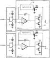
参见图2,本发明实施例公开了一种数字音频功放,包括PWM调制器(图2中未示出)、两路DAC电流源和两路功放环路,其中:Referring to FIG. 2, an embodiment of the present invention discloses a digital audio power amplifier, including a PWM modulator (not shown in FIG. 2), two DAC current sources and two power amplifier loops, wherein:
数字音频信号经过所述PWM调制器调制后输出PWMP波和PWMN波,所述PWMP波经过一路DAC电流源、一路功放环路处理后输出电压VOUTP,所述PWMN波经过另一路DAC电流源、另一路功放环路处理后输出电压VOUTN;The digital audio signal outputs PWMP wave and PWMN wave after being modulated by the PWM modulator. The PWMP wave is processed by one DAC current source and one power amplifier loop to output the voltage VOUTP , and the PWMN wave passes through another DAC current source, The output voltage VOUTN after processing by another power amplifier loop;
每一路功放环路都包括运放U1、电容C1、功放输出级11、电阻R1、电阻R2、噪声控制单元12,其中:Each power amplifier loop includes an operational amplifier U1, a capacitor C1, a power
运放U1的反相输入端分别连接到电容C1的一端、噪声控制单元12的一端以及前级的所述DAC电流源的输出端;The inverting input end of the operational amplifier U1 is respectively connected to one end of the capacitor C1, one end of the
运放U1的输出端分别连接到功放输出级11的控制端和电容C1的另一端;The output end of the operational amplifier U1 is respectively connected to the control end of the power
功放输出级11的输出端依次经过电阻R1、电阻R2接地;The output terminal of the power
噪声控制单元12的另一端连接到电阻R1与电阻R2的连结点;The other end of the
电阻R1、R2的阻值设置满足R1/R2=(N-2)/2,N>2;参考电压VREF加在运放U1的同相输入端,参考电压VREF=PVDD/N,PVDD为功放输出级11的电源电压;The resistance settings of resistors R1 and R2 satisfy R1/R2=(N-2)/2, N>2; the reference voltage VREF is applied to the non-inverting input of the operational amplifier U1, the reference voltage VREF =PVDD/N, and PVDD is The supply voltage of the power
在一个实施方式中,噪声控制单元12为电阻模块。In one embodiment, the
在本发明实施例中,由于两路DAC电流源、两路功放环路的电路结构均相同,下面,仅以PWMP波→DAC电流源→功放环路→VOUTP这一路为例,详述本发明实施例所述数字音频功放的工作原理:In the embodiment of the present invention, since the circuit structures of the two DAC current sources and the two power amplifier loops are the same, the following only takes the path PWMP wave→DAC current source→power amplifier loop→VOUTP as an example to describe the The working principle of the digital audio power amplifier described in the embodiment of the invention:
相较于现有的功放环路,本发明实施例中公开的功放环路增加电阻R1和R2形成分压,电阻R1、R2的阻值大小以及功放环路的参考电压VREF大小以满足“功放环路中电容充放电平衡;以及当VOUTP达到电源电压PVDD时,功放环路的参考电压VREF小于PVDD/2”为准进行设置,本发明实施例中具体设置R1/R2=(N-2)/2,N>2,VREF=PVDD/N。为方便实际应用和简化计算,本发明实施例推荐取N为整数。例如,取N=3,即设置R2=2*R1,此时参考电压VREF=PVDD/3,这就意味着当PVDD等于10V时,VREF约等于3.33V,在电流源和功放环路能支持的最大工作电压等于5V的情况下,电路仍能正常工作。Compared with the existing power amplifier loop, the power amplifier loop disclosed in the embodiment of the present invention adds resistors R1 and R2 to form a voltage divider. The resistance values of the resistors R1 and R2 and the reference voltageVREF of the power amplifier loop meet the requirements of The capacitor charge and discharge balance in the power amplifier loop; and when VOUTP reaches the power supply voltage PVDD, the reference voltage VREF of the power amplifier loop is set to be less than PVDD/2". In the embodiment of the present invention, R1/R2 = (N -2)/2, N>2, VREF =PVDD/N. To facilitate practical applications and simplify calculations, it is recommended that N be an integer in the embodiment of the present invention. For example, take N=3, that is, set R2=2*R1, at this time, the reference voltage VREF =PVDD/3, which means that when PVDD is equal to 10V, VREF is about 3.33V, in the current source and power amplifier loop When the maximum operating voltage that can be supported is equal to 5V, the circuit can still work normally.
接下来,针对PWMP波→DAC电流源→功放环路→VOUTP这一路,以N=3为例,验证当R2=2*R1,VREF=PVDD/3时,数字音频功放能够正常工作。具体验证过程如下:Next, for the path of PWMP wave→DAC current source→power amplifier loop→VOUTP , taking N=3 as an example, it is verified that when R2=2*R1,VREF =PVDD/3, the digital audio power amplifier can work normally. The specific verification process is as follows:
定义噪声控制单元12的等效电阻为RF;DAC电流源的输出电流为IDAC;VOUT=VOUTP-VOUTN;电容C1的一个充放电周期T分为t1、t2、t3、t4四个时段,对应的PWMP波、VOUT、电容C1的充放电电流IC1、电容C1右边节点电位VC1的波形图如图3所示:Define the equivalent resistance of the
t1时段:PWMP波=高电平逻辑“1”,VOUT=高电平逻辑“1”,电流IDAC给电容C1充电,同时功放输出端(即功放输出级的输出端)通过等效电阻RF给电容C1充电(VOUT=高电平逻辑“1”时,VOUTP电压为PVDD,由于电阻R1和R2形成分压,所以电阻R1与R2的连结点电位等于PVDD*2/3;运放U1的反相输入端电位与同相输入端电位相等,为VREF=PVDD/3;由此可得,等效电阻RF两端电位差即为PVDD/3-PVDD*2/3=-1/3*PVDD,功放输出端通过等效电阻RF给电容C1充电的电流大小即为1/3*PVDD/RF),此时电容C1上的电流为t1 period: PWMP wave = high-level logic "1", VOUT = high-level logic "1", the current IDAC charges the capacitor C1, and the output terminal of the power amplifier (ie the output terminal of the power amplifier output stage) passes through the equivalent resistance RF charges capacitor C1 (VOUT = high level logic "1", VOUTP voltage is PVDD, since resistors R1 and R2 form a voltage divider, the potential of the connection point between resistors R1 and R2 is equal to PVDD*2/3; The potential of the inverting input terminal of the op amp U1 is equal to the potential of the non-inverting input terminal, which is VREF =PVDD/3; from this, the potential difference between the two ends of the equivalent resistance RF is PVDD/3-PVDD*2/3= -1/3*PVDD, the current of the power amplifier output to charge the capacitor C1 through the equivalent resistor RF is 1/3*PVDD/RF ), at this time the current on the capacitor C1 is
IC1_t1=IDAC+1/3*PVDD/RF 式(2.1)IC1_t1 =IDAC +1/3*PVDD /RF formula (2.1)
t2时段:PWMP波=高电平逻辑“1”,VOUT=低电平逻辑“0”,电流IDAC给电容C1充电,同时功放输出端通过等效电阻RF给电容C1放电(VOUT=低电平逻辑“0”时,VOUTP电压为零,由于电阻R1与R2的连结点电位也为零;运放U1的反相输入端电位与同相输入端电位相等,为VREF=PVDD/3;由此可得,等效电阻RF两端电位差即为PVDD/3,功放输出端通过等效电阻RF给电容C1放电的电流大小即为1/3*PVDD/R),此时电容C1上的电流为t2 period: PWMP wave = high-level logic "1", VOUT = low-level logic "0", the current IDAC charges the capacitor C1, and the output of the power amplifier discharges the capacitor C1 through the equivalent resistance RF (VOUT = When the low-level logic is "0", the voltage of VOUTP is zero, because the potential of the connection point of the resistors R1 and R2 is also zero; the potential of the inverting input terminal of the op amp U1 is equal to the potential of the non-inverting input terminal, which is VREF =PVDD /3; from this, the potential difference between the two ends of the equivalent resistor RF is PVDD/3, and the magnitude of the current that the output of the power amplifier discharges to the capacitor C1 through the equivalent resistor RF is 1/3*PVDD/R), At this time, the current on capacitor C1 is
IC1_t2=IDAC-1/3*PVDD/RF 式(2.2)IC1_t2 =IDAC -1/3*PVDD /RF formula (2.2)
t3时段:PWMP波=低电平逻辑“0”,VOUT=低电平逻辑“0”,电流IDAC给电容C1放电,同时功放输出端通过等效电阻RF给电容C1放电(与t2时段同理,当VOUT=低电平逻辑“0”时,功放输出端通过等效电阻RF给电容C1放电的电流大小即为1/3*PVDD/RF),此时电容C1上的电流为t3 period: PWMP wave = low-level logic "0", VOUT = low-level logic "0", the current IDAC discharges the capacitor C1, and the output of the power amplifier discharges the capacitor C1 through the equivalent resistance RF (same as t2). The period is the same, when VOUT = low level logic "0", the current of the power amplifier output to discharge the capacitor C1 through the equivalent resistance RF is 1/3*PVDD/RF ). At this time, the capacitor C1 is on The current is
IC1_t3=-IDAC-1/3*PVDD/RF 式(2.3)IC1_t3 = -IDAC -1/3*PVDD /RF formula (2.3)
t4时段:PWMP波=低电平逻辑“0”,VOUT=高电平逻辑“1”,电流IDAC给电容C1放电,同时功放输出端通过等效电阻RF给电容C1充电(与t1时段同理,当VOUT=高电平逻辑“1”时,功放输出端通过等效电阻RF给电容C1充电的电流大小即为1/3*PVDD/RF),此时电容C1上的电流为t4 period: PWMP wave = low-level logic "0", VOUT = high-level logic "1", the current IDAC discharges the capacitor C1, and the output of the power amplifier charges the capacitor C1 through the equivalent resistance RF (same as t1). Similarly for the time period, when VOUT = high level logic "1", the current of the power amplifier output to charge the capacitor C1 through the equivalent resistance RF is 1/3*PVDD /RF ). The current is
IC1_t4=-IDAC+1/3*PVDD/RF 式(2.4)数字音频功放正常工作时,电容C1在一个充放电周期T内充放电平衡,有IC1_t4 = -IDAC +1/3*PVDD /RF formula (2.4) When the digital audio power amplifier is working normally, the capacitor C1 is charged and discharged in a charge and discharge cycle T, and there are
IC1_t1*t1+IC1_t2*t2=-IC1_t3*t3-IC1_t4*t4 式(2.5)IC1_t1 *t1+IC1_t2 *t2=-IC1_t3 *t3-IC1_t4 *t4 Equation (2.5)
将式(2.1)~式(2.4)代入式(2.5),整理可得Substituting equations (2.1) to (2.4) into equations (2.5), we can get
IDAC*(t1+t2)-IDAC*(t3+t4)=1/3*PVDD/RF*(t2+t3)-1/3*PVDD/RF*(t1+t4) 式(2.6)IDAC *(t1 +t2 )-IDAC *(t3 +t4 )=1/3*PVDD /RF *(t2 +t3 )-1/3*PVDD /RF *(t1 +t4 ) Equation (2.6)
用DIN表示PWMP波输入占空比,则t1+t2=DIN*T,t3+t4=(1-DIN)*T,用DOUT表示PWMP波输出占空比,则t1+t4=DOUT*T,t2+t3=(1-DOUT)*T,基于此,式(2.6)整理可得Use DIN to represent the PWMP wave input duty cycle, then t1+t2=DIN *T, t3+t4=(1-DIN )*T, and use DOUT to represent the PWMP wave output duty cycle, then t1+t4= DOUT *T, t2+t3=(1-DOUT )*T, based on this, formula (2.6) can be sorted out

又由于VOUTP=DOUT*PVDD,则式(2.7)进一步整理可得And since VOUTP =DOUT *PVDD, the formula (2.7) can be further sorted out to obtain

式(2.8)表明VOUTP是一个以1/2*PVDD为共模点,50%输入占空比为中心的信号。Equation (2.8) shows that VOUTP is a signal centered on 1/2*PVDD as the common-mode point and 50% input duty cycle.
同理,可得VOUTN的关系式,
当设置R2=2*R1,VREF=PVDD/3时,从VOUTP和VOUTN的关系式可以看出,该数字音频功放能够正常工作,电容C1在一个充放电周期T内充放电平衡。When setting R2=2*R1 and VREF =PVDD/3, it can be seen from the relationship between VOUTP and VOUTN that the digital audio power amplifier can work normally, and the capacitor C1 is charged and discharged in a charge-discharge cycle T to balance.
本发明实施例中设置R1/R2=(N-2)/2,N>2,VREF=PVDD/N,N的取值越大,参考电压VREF的值越小,DAC电流源和功放环路留有的电压余量就越大,由于要预留的电压余量一般是固定的,所以电阻R1、R2一般推荐采用固定电阻。In the embodiment of the present invention, set R1/R2=(N-2)/2, N>2, VREF =PVDD/N, the larger the value of N, the smaller the value of the reference voltage VREF , the DAC current source and power amplifier The larger the voltage margin left in the loop, because the voltage margin to be reserved is generally fixed, so the resistors R1 and R2 are generally recommended to use fixed resistors.
本发明实施例中,噪声控制单元12的等效电阻RF阻值大小直接影响功放环路的增益,具体分析如下:In the embodiment of the present invention, the value of the equivalent resistance RF of the
将VOUTP、VOUTN的关系式代入VOUT=VOUTP-VOUTN,可得Substitute the relationship between VOUTP and VOUTN into VOUT =VOUTP -VOUTN , we can get
VOUT=3*RF*IDAC(2*DIN-1) 式(2.9)VOUT = 3*RF *IDAC (2*DIN -1) Equation (2.9)
由式(2.9)可知,功放环路的增益为3*RF*IDAC,与RF相关。通过调整噪声控制单元12的等效电阻RF阻值大小,可任意调整功放环路的增益。It can be known from equation (2.9) that the gain of the power amplifier loop is 3*RF *IDAC , which is related toRF . By adjusting the value of the equivalent resistance RF of the
高压数字音频功放中DAC电流源的噪声对输出噪声的影响最大,减小功放环路的增益能有效降低输出噪声,但是如果功放环路的增益过小,则功放环路在不失真的情况下只能输出非常小的功率,不满足实际应用中提升喇叭响度的要求,因此需要保证输出信号的信噪比(输出噪声在数字音频功放输出信号中所占的比重)保持在比较理想的状态。数字音频信号的幅值越小,功放环路输出功率越大,输出噪声在数字音频功放输出信号中所占的比重越大,越是需要更进一步降低输出噪声,所以需要根据数字音频信号的幅值大小来合理设置功放环路的增益,在输出功率和输出噪声之间取得良好的平衡,既保证了较大的输出功率,也降低了输出信号的噪声。The noise of the DAC current source in the high-voltage digital audio power amplifier has the greatest impact on the output noise. Reducing the gain of the power amplifier loop can effectively reduce the output noise. However, if the gain of the power amplifier loop is too small, the power amplifier loop will not be distorted. It can only output very small power, which does not meet the requirements of improving loudspeaker loudness in practical applications. Therefore, it is necessary to ensure that the signal-to-noise ratio of the output signal (the proportion of output noise in the output signal of the digital audio power amplifier) is kept in an ideal state. The smaller the amplitude of the digital audio signal, the greater the output power of the power amplifier loop, the greater the proportion of output noise in the output signal of the digital audio power amplifier, the more it is necessary to further reduce the output noise, so it is necessary to reduce the output noise according to the amplitude of the digital audio signal. The gain of the power amplifier loop is reasonably set by the value of the value, and a good balance is achieved between the output power and the output noise, which not only ensures a large output power, but also reduces the noise of the output signal.
噪声控制单元12可以为固定电阻模块,即阻值固定的电阻模块,但这样会导致数字音频功放对输入数字音频信号的适用范围有限,因此,本发明实施例推荐噪声控制单元12采用可调电阻模块,即阻值可调节的电阻模块,其阻值大小随所述数字音频信号的幅值降低而减小。The
进一步的,本发明实施例推荐设置可调电阻模块12的阻值随所述数字音频信号的幅值变化呈阶跃变化。此时噪声控制单元12的拓扑结构可采用如图4所示,噪声控制单元12包括k个串联电阻RF0~RF(k-1),k≥1,其中电阻RF1~RF(k-1)中的每一个都并联一个开关;为便于描述,将电阻RFX(X=1、2、…、k-1)并联的开关标识为TX,图4仅以k=3作为示例。RF的阻值随噪声控制单元12内开关组合状态的变化而变化,噪声控制单元12内的开关组合状态取决于数字音频信号的幅值大小。Further, in the embodiment of the present invention, it is recommended to set the resistance value of the
举个例子,假设k=3,则当开关T1和T2均断开时,功放环路的增益为3*(RF0+RF1+RF2)*IDAC;当开关T2导通、T1断开时,功放环路的增益为3*(RF0+RF1)*IDAC;当开关T1和T2均导通时,功放环路的增益为3*RF0*IDAC。设置电阻为RF1=RF0,RF2=2*RF0,则有下表1所示:For example, assuming k=3 , whenboth switches T1 and T2 are off, the gain of the power amplifier loop is 3*(RF0 +RF1 +RF2 )*IDAC ; when switch T2 is on , when T1 is disconnected, the gain of the power amplifier loop is 3*(RF0 +RF1 )*IDAC ; when both switches T1 and T2 are turned on, the gain of the power amplifier loop is3 *RF0 *IDAC . Set the resistance as RF1 = RF0 , RF2 = 2*RF0 , as shown in Table 1 below:
对应表1,当数字音频信号的幅值大于设定阈值1时,让功放环路工作于上述状态1;当数字音频信号的幅值低于设定阈值1但大于设定阈值2时(阈值1大于阈值2),经过一定延迟时间后,在数字音频信号过零处再切换电路状态(增益调整如果不在信号过零处,可能导致输出信号存在突变,影响体验),让功放环路工作于上述状态2;当数字音频信号的幅值低于设定阈值2时,经过一定延迟时间后,在数字音频信号过零处再切换电路状态,让功放环路工作于上述状态3。由此可见,当噪声控制单元12采用可调电阻模块,噪声控制单元12需要延时到输入到DAC电流源的数字音频信号过零点时调整自身阻值大小。Corresponding to Table 1, when the amplitude of the digital audio signal is greater than the
另外需要说明的是,减小功放的增益能有效降低输出噪声,但是为满足实际应用中提升喇叭响度的要求,避免喇叭响度忽大忽小的问题,有必要尽量保证数字音频功放的总增益不变,因此本发明实施例在减小功放环路的增益的同时,可以对应增大数字音频功放中的PWM调制器的增益。例如,对应表1,功放环路工作于上述状态1时,PWM调制器的增益不作处理;功放环路工作于上述状态2时,PWM调制器的增益增加到原来的2倍;功放环路工作于上述状态3时,PWM调制器的增益增加到原来的4倍。In addition, it should be noted that reducing the gain of the power amplifier can effectively reduce the output noise. However, in order to meet the requirements of improving the loudness of the speaker in practical applications and avoid the problem of the loudness of the speaker fluctuating, it is necessary to try to ensure that the total gain of the digital audio power amplifier does not Therefore, the embodiment of the present invention can correspondingly increase the gain of the PWM modulator in the digital audio power amplifier while reducing the gain of the power amplifier loop. For example, corresponding to Table 1, when the power amplifier loop works in the
如图5所示,本发明实施例还公开了一种功放环路,包括运放U1、电容C1、功放输出级、电阻R1、电阻R2和噪声控制单元,其中:As shown in FIG. 5 , an embodiment of the present invention further discloses a power amplifier loop, including an operational amplifier U1, a capacitor C1, a power amplifier output stage, a resistor R1, a resistor R2 and a noise control unit, wherein:
运放U1的反相输入端分别连接到电容C1的一端、所述噪声控制单元的一端以及前级的DAC电流源的输出端;The inverting input end of the operational amplifier U1 is respectively connected to one end of the capacitor C1, one end of the noise control unit and the output end of the front-stage DAC current source;
运放U1的输出端分别连接到所述功放输出级的控制端和电容C1的另一端;The output end of the operational amplifier U1 is respectively connected to the control end of the output stage of the power amplifier and the other end of the capacitor C1;
所述功放输出级的输出端依次经过电阻R1、电阻R2接地;The output end of the power amplifier output stage is grounded through the resistor R1 and the resistor R2 in sequence;
所述噪声控制单元的另一端连接到电阻R1与电阻R2的连结点;The other end of the noise control unit is connected to the connection point of the resistor R1 and the resistor R2;
电阻R1、R2的阻值设置满足R1/R2=(N-2)/2,N>2;参考电压加在运放U1的同相输入端,参考电压等于PVDD/N,PVDD为所述功放输出级的电源电压;The resistance values of resistors R1 and R2 are set to satisfy R1/R2=(N-2)/2, N>2; the reference voltage is applied to the non-inverting input of the operational amplifier U1, the reference voltage is equal to PVDD/N, and PVDD is the output of the power amplifier level supply voltage;
所述噪声控制单元为电阻模块。The noise control unit is a resistance module.
可选的,所述噪声控制单元为可调电阻模块,其阻值大小随所述数字音频信号的幅值的降低而减小。Optionally, the noise control unit is an adjustable resistance module, the resistance value of which decreases as the amplitude of the digital audio signal decreases.
可选的,所述可调电阻模块的阻值随所述数字音频信号幅值的变化呈阶跃变化。Optionally, the resistance value of the adjustable resistance module changes in steps with the change of the amplitude of the digital audio signal.
可选的,所述噪声控制单元包括多个串联电阻,其中每一个电阻都各自并联一个开关;不同开关的开关状态取决于所述数字音频信号的幅值大小。Optionally, the noise control unit includes a plurality of resistors in series, wherein each resistor is connected in parallel with a switch; the switch states of different switches depend on the amplitude of the digital audio signal.
可选的,所述噪声控制单元延时到所述数字音频信号过零点时再调整自身阻值大小。Optionally, the noise control unit adjusts its own resistance value after delaying until the digital audio signal crosses a zero point.
本说明书中各个数字音频功放实施例采用递进的方式描述,每个数字音频功放实施例重点说明的都是与其他数字音频功放实施例的不同之处,各个数字音频功放实施例之间相同相似部分互相参见即可。对于功放环路实施例而言,由于其与数字音频功放实施例公开的技术内容相对应,所以描述的比较简单,相关之处参见数字音频功放实施例部分的相关说明即可。Each digital audio power amplifier embodiment in this specification is described in a progressive manner, and each digital audio power amplifier embodiment focuses on the differences from other digital audio power amplifier embodiments, and the digital audio power amplifier embodiments are the same and similar. Some can refer to each other. As for the embodiment of the power amplifier loop, since it corresponds to the technical content disclosed in the embodiment of the digital audio power amplifier, the description is relatively simple, and for relevant details, please refer to the relevant description of the embodiment of the digital audio power amplifier.
在本文中,诸如第一和第二等之类的关系术语仅仅用来将一个实体或者操作与另一个实体或操作区分开来,而不一定要求或者暗示这些实体或操作之间存在任何这种实际的关系或者顺序。而且,术语“包括”、“包含”或者其任何其他变体意在涵盖非排他性的包含,从而使得包括一系列要素的过程、方法、商品或者设备不仅包括那些要素,而且还包括没有明确列出的其他要素,或者是还包括为这种过程、方法、商品或者设备所固有的要素。在没有更多限制的情况下,由语句“包括一个”限定的要素,并不排除在包括要素的过程、方法、商品或者设备中还存在另外的相同要素。In this document, relational terms such as first and second, etc. are used only to distinguish one entity or operation from another entity or operation, and do not necessarily require or imply any such existence between these entities or operations. The actual relationship or sequence. Moreover, the terms "comprising", "comprising" or any other variation thereof are intended to encompass non-exclusive inclusion such that a process, method, article of manufacture or device comprising a list of elements includes not only those elements, but also includes not explicitly listed or other elements inherent to such a process, method, commodity or apparatus. Without further limitation, an element qualified by the phrase "comprising a" does not preclude the presence of additional identical elements in the process, method, article of manufacture, or device that includes the element.
专业人员还可以进一步意识到,结合本文中所公开的实施例描述的各示例的单元及算法步骤,能够以电子硬件、计算机软件或者二者的结合来实现,为了清楚地说明硬件和软件的可互换性,在上述说明中已经按照功能一般性地描述了各示例的组成及步骤。这些功能究竟以硬件还是软件方式来执行,取决于技术方案的特定应用和设计约束条件。专业技术人员可以对每个特定的应用来使用不同方法来实现所描述的功能,但是这种实现不应认为超出本发明的范围。Professionals may further realize that the units and algorithm steps of each example described in conjunction with the embodiments disclosed herein can be implemented in electronic hardware, computer software, or a combination of the two, in order to clearly illustrate the possibilities of hardware and software. Interchangeability, the above description has generally described the components and steps of each example in terms of functionality. Whether these functions are performed in hardware or software depends on the specific application and design constraints of the technical solution. Skilled artisans may implement the described functionality using different methods for each particular application, but such implementations should not be considered beyond the scope of the present invention.
对所公开的实施例的上述说明,使本领域专业技术人员能够实现或使用本发明。对这些实施例的多种修改对本领域的专业技术人员来说将是显而易见的,本文中所定义的一般原理可以在不脱离本发明实施例的精神或范围的情况下,在其它实施例中实现。因此,本发明实施例将不会被限制于本文所示的这些实施例,而是要符合与本文所公开的原理和新颖特点相一致的最宽的范围。The above description of the disclosed embodiments enables any person skilled in the art to make or use the present invention. Various modifications to these embodiments will be readily apparent to those skilled in the art, and the general principles defined herein may be implemented in other embodiments without departing from the spirit or scope of the embodiments of the present invention . Thus, embodiments of the present invention are not to be limited to those shown herein, but are to be accorded the widest scope consistent with the principles and novel features disclosed herein.
Claims (10)
Translated fromChinesePriority Applications (4)
| Application Number | Priority Date | Filing Date | Title |
|---|---|---|---|
| CN201911217916.1ACN110868162A (en) | 2019-11-29 | 2019-11-29 | A digital audio power amplifier and power amplifier loop |
| KR1020227016221AKR20220082048A (en) | 2019-11-29 | 2020-11-18 | Digital Audio Power Amplifiers and Power Amplifier Loops |
| PCT/CN2020/129674WO2021104119A1 (en) | 2019-11-29 | 2020-11-18 | Digital audio power amplifier and power amplifier loop |
| US17/756,601US12301181B2 (en) | 2019-11-29 | 2020-11-18 | Digital audio power amplifier and power amplifier loop |
Applications Claiming Priority (1)
| Application Number | Priority Date | Filing Date | Title |
|---|---|---|---|
| CN201911217916.1ACN110868162A (en) | 2019-11-29 | 2019-11-29 | A digital audio power amplifier and power amplifier loop |
Publications (1)
| Publication Number | Publication Date |
|---|---|
| CN110868162Atrue CN110868162A (en) | 2020-03-06 |
Family
ID=69657348
Family Applications (1)
| Application Number | Title | Priority Date | Filing Date |
|---|---|---|---|
| CN201911217916.1APendingCN110868162A (en) | 2019-11-29 | 2019-11-29 | A digital audio power amplifier and power amplifier loop |
Country Status (4)
| Country | Link |
|---|---|
| US (1) | US12301181B2 (en) |
| KR (1) | KR20220082048A (en) |
| CN (1) | CN110868162A (en) |
| WO (1) | WO2021104119A1 (en) |
Cited By (1)
| Publication number | Priority date | Publication date | Assignee | Title |
|---|---|---|---|---|
| WO2021104119A1 (en)* | 2019-11-29 | 2021-06-03 | 上海艾为电子技术股份有限公司 | Digital audio power amplifier and power amplifier loop |
Citations (6)
| Publication number | Priority date | Publication date | Assignee | Title |
|---|---|---|---|---|
| EP3229371A1 (en)* | 2016-04-06 | 2017-10-11 | Nxp B.V. | Audio amplifier system |
| CN109068237A (en)* | 2018-08-27 | 2018-12-21 | 上海艾为电子技术股份有限公司 | A kind of digital audio power amplification system |
| CN208540150U (en)* | 2018-08-27 | 2019-02-22 | 上海艾为电子技术股份有限公司 | A kind of digital audio power amplification system |
| CN208754539U (en)* | 2018-08-27 | 2019-04-16 | 上海艾为电子技术股份有限公司 | A kind of digital audio power amplification system |
| CN109660917A (en)* | 2018-12-26 | 2019-04-19 | 上海艾为电子技术股份有限公司 | A kind of high-voltage digital audio power amplification system |
| CN110212871A (en)* | 2019-06-12 | 2019-09-06 | 上海艾为电子技术股份有限公司 | A kind of audio-frequency power amplifier and its gain control circuit and control method |
Family Cites Families (6)
| Publication number | Priority date | Publication date | Assignee | Title |
|---|---|---|---|---|
| US7262658B2 (en)* | 2005-07-29 | 2007-08-28 | Texas Instruments Incorporated | Class-D amplifier system |
| US8581661B2 (en) | 2011-10-24 | 2013-11-12 | Conexant Systems, Inc. | Audio programmable gain amplifier with automatic reconfiguration |
| CN104467710B (en)* | 2013-09-12 | 2018-05-04 | 意法半导体研发(深圳)有限公司 | Method and circuit for removing POP noise in audio equipment |
| CN106255005B (en) | 2016-09-23 | 2020-10-30 | 深圳市冠旭电子股份有限公司 | An audio ground isolation differential circuit and a speaker |
| GB2565293A (en) | 2017-08-07 | 2019-02-13 | Reid Acoustic Designs Ltd | An error amplifier |
| CN110868162A (en) | 2019-11-29 | 2020-03-06 | 上海艾为电子技术股份有限公司 | A digital audio power amplifier and power amplifier loop |
- 2019
- 2019-11-29CNCN201911217916.1Apatent/CN110868162A/enactivePending
- 2020
- 2020-11-18KRKR1020227016221Apatent/KR20220082048A/ennot_activeCeased
- 2020-11-18USUS17/756,601patent/US12301181B2/enactiveActive
- 2020-11-18WOPCT/CN2020/129674patent/WO2021104119A1/ennot_activeCeased
Patent Citations (6)
| Publication number | Priority date | Publication date | Assignee | Title |
|---|---|---|---|---|
| EP3229371A1 (en)* | 2016-04-06 | 2017-10-11 | Nxp B.V. | Audio amplifier system |
| CN109068237A (en)* | 2018-08-27 | 2018-12-21 | 上海艾为电子技术股份有限公司 | A kind of digital audio power amplification system |
| CN208540150U (en)* | 2018-08-27 | 2019-02-22 | 上海艾为电子技术股份有限公司 | A kind of digital audio power amplification system |
| CN208754539U (en)* | 2018-08-27 | 2019-04-16 | 上海艾为电子技术股份有限公司 | A kind of digital audio power amplification system |
| CN109660917A (en)* | 2018-12-26 | 2019-04-19 | 上海艾为电子技术股份有限公司 | A kind of high-voltage digital audio power amplification system |
| CN110212871A (en)* | 2019-06-12 | 2019-09-06 | 上海艾为电子技术股份有限公司 | A kind of audio-frequency power amplifier and its gain control circuit and control method |
Non-Patent Citations (1)
| Title |
|---|
| 赵海亮;刘诺;周长胜;: "D类功放中输入斩波运放电路的设计", no. 06* |
Cited By (2)
| Publication number | Priority date | Publication date | Assignee | Title |
|---|---|---|---|---|
| WO2021104119A1 (en)* | 2019-11-29 | 2021-06-03 | 上海艾为电子技术股份有限公司 | Digital audio power amplifier and power amplifier loop |
| US12301181B2 (en) | 2019-11-29 | 2025-05-13 | Shanghai Awinic Technology Co., LTD | Digital audio power amplifier and power amplifier loop |
Also Published As
| Publication number | Publication date |
|---|---|
| US20220416734A1 (en) | 2022-12-29 |
| WO2021104119A1 (en) | 2021-06-03 |
| US12301181B2 (en) | 2025-05-13 |
| KR20220082048A (en) | 2022-06-16 |
Similar Documents
| Publication | Publication Date | Title |
|---|---|---|
| TWI499202B (en) | Class-d power amplifier capable of reducing electromagnetic interference and triangular wave generator thereof | |
| KR101814311B1 (en) | Class-d amplifier circuits | |
| TWI661669B (en) | Multi-stage amplifier | |
| CN103326680B (en) | D-type audio power amplifier and audio signal processing method thereof | |
| CN109660917B (en) | High-voltage digital audio power amplifier system | |
| CN206272476U (en) | Jitter frequency control circuit and switching power supply | |
| CN112713858B (en) | Oscillator | |
| CN102931837A (en) | Duty cycle adjustment circuit and signal generating device | |
| WO2024041267A1 (en) | Audio power amplifier circuit, and duty ratio modulation circuit and noise suppression circuit thereof | |
| CN109639135B (en) | Charge pump circuit | |
| CN110868162A (en) | A digital audio power amplifier and power amplifier loop | |
| US20060071697A1 (en) | Pwm generator | |
| US9825600B2 (en) | Class D amplifier and electronic devices including the same | |
| CN119109319A (en) | Multi-level buck converter | |
| TW201925953A (en) | Method and circuit for low-noise reference signal generation | |
| CN102938635A (en) | Frequency multiplication circuit | |
| CN222215704U (en) | Class D amplifier circuit, audio processing chip, and information processing apparatus | |
| TW201735529A (en) | Programmable amplifier circuit | |
| CN209448886U (en) | A kind of high-voltage digital audio power amplification system | |
| CN209314030U (en) | A kind of high-voltage digital audio power amplification system | |
| CN108304021B (en) | Clamping circuit | |
| CN110829983A (en) | Digital audio power amplifier | |
| US20250219600A1 (en) | Amplification device and operation method thereof | |
| CN212850438U (en) | A waveform generating circuit and electronic equipment | |
| CN210693873U (en) | Automatic correction circuit for output offset voltage of class-D power amplifier circuit |
Legal Events
| Date | Code | Title | Description |
|---|---|---|---|
| PB01 | Publication | ||
| PB01 | Publication | ||
| SE01 | Entry into force of request for substantive examination | ||
| SE01 | Entry into force of request for substantive examination | ||
| RJ01 | Rejection of invention patent application after publication | Application publication date:20200306 | |
| RJ01 | Rejection of invention patent application after publication |