CN110838565B - Metal mask, display panel and display device - Google Patents
Metal mask, display panel and display deviceDownload PDFInfo
- Publication number
- CN110838565B CN110838565BCN201911172698.4ACN201911172698ACN110838565BCN 110838565 BCN110838565 BCN 110838565BCN 201911172698 ACN201911172698 ACN 201911172698ACN 110838565 BCN110838565 BCN 110838565B
- Authority
- CN
- China
- Prior art keywords
- metal
- present
- groove
- display panel
- reticle
- Prior art date
- Legal status (The legal status is an assumption and is not a legal conclusion. Google has not performed a legal analysis and makes no representation as to the accuracy of the status listed.)
- Active
Links
Images


Classifications
- C—CHEMISTRY; METALLURGY
- C23—COATING METALLIC MATERIAL; COATING MATERIAL WITH METALLIC MATERIAL; CHEMICAL SURFACE TREATMENT; DIFFUSION TREATMENT OF METALLIC MATERIAL; COATING BY VACUUM EVAPORATION, BY SPUTTERING, BY ION IMPLANTATION OR BY CHEMICAL VAPOUR DEPOSITION, IN GENERAL; INHIBITING CORROSION OF METALLIC MATERIAL OR INCRUSTATION IN GENERAL
- C23C—COATING METALLIC MATERIAL; COATING MATERIAL WITH METALLIC MATERIAL; SURFACE TREATMENT OF METALLIC MATERIAL BY DIFFUSION INTO THE SURFACE, BY CHEMICAL CONVERSION OR SUBSTITUTION; COATING BY VACUUM EVAPORATION, BY SPUTTERING, BY ION IMPLANTATION OR BY CHEMICAL VAPOUR DEPOSITION, IN GENERAL
- C23C14/00—Coating by vacuum evaporation, by sputtering or by ion implantation of the coating forming material
- C23C14/04—Coating on selected surface areas, e.g. using masks
- C23C14/042—Coating on selected surface areas, e.g. using masks using masks
- H—ELECTRICITY
- H10—SEMICONDUCTOR DEVICES; ELECTRIC SOLID-STATE DEVICES NOT OTHERWISE PROVIDED FOR
- H10K—ORGANIC ELECTRIC SOLID-STATE DEVICES
- H10K50/00—Organic light-emitting devices
- H10K50/80—Constructional details
- H10K50/84—Passivation; Containers; Encapsulations
- H10K50/844—Encapsulations
- H—ELECTRICITY
- H10—SEMICONDUCTOR DEVICES; ELECTRIC SOLID-STATE DEVICES NOT OTHERWISE PROVIDED FOR
- H10K—ORGANIC ELECTRIC SOLID-STATE DEVICES
- H10K59/00—Integrated devices, or assemblies of multiple devices, comprising at least one organic light-emitting element covered by group H10K50/00
- H10K59/10—OLED displays
- H10K59/12—Active-matrix OLED [AMOLED] displays
- H—ELECTRICITY
- H10—SEMICONDUCTOR DEVICES; ELECTRIC SOLID-STATE DEVICES NOT OTHERWISE PROVIDED FOR
- H10K—ORGANIC ELECTRIC SOLID-STATE DEVICES
- H10K71/00—Manufacture or treatment specially adapted for the organic devices covered by this subclass
- H—ELECTRICITY
- H10—SEMICONDUCTOR DEVICES; ELECTRIC SOLID-STATE DEVICES NOT OTHERWISE PROVIDED FOR
- H10K—ORGANIC ELECTRIC SOLID-STATE DEVICES
- H10K59/00—Integrated devices, or assemblies of multiple devices, comprising at least one organic light-emitting element covered by group H10K50/00
- H10K59/80—Constructional details
- H10K59/87—Passivation; Containers; Encapsulations
- H10K59/873—Encapsulations
Landscapes
- Chemical & Material Sciences (AREA)
- Engineering & Computer Science (AREA)
- Chemical Kinetics & Catalysis (AREA)
- Materials Engineering (AREA)
- Mechanical Engineering (AREA)
- Metallurgy (AREA)
- Organic Chemistry (AREA)
- Physics & Mathematics (AREA)
- Optics & Photonics (AREA)
- Microelectronics & Electronic Packaging (AREA)
- Manufacturing & Machinery (AREA)
- Electroluminescent Light Sources (AREA)
Abstract
Translated fromChinese
Description
Translated fromChinese技术领域technical field
本发明涉及显示制作技术领域,具体的,本发明涉及金属掩模版、显示面板和显示装置。The present invention relates to the technical field of display manufacturing, and in particular, the present invention relates to a metal mask, a display panel and a display device.
背景技术Background technique
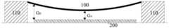
现阶段的有源矩阵有机发光二极体(AMOLED)薄膜封装技术中,采用金属掩模版(Mask)对封装无机层进行图案化。参考图1,由于金属掩模版100在重力作用下会出现下垂现象,造成其中心区A和边缘区B与衬底200之间的间隙(Gap)值G不同,从而导致不同位置处的封装无机层的膜厚度不均匀,特别是参考图2,造成膜厚度在10%~90%的厚度渐变区(Shadow)C的不均匀性范围越长。In the current active matrix organic light emitting diode (AMOLED) thin film encapsulation technology, a metal mask (Mask) is used to pattern the encapsulated inorganic layer. Referring to FIG. 1 , due to the sagging phenomenon of the
发明内容SUMMARY OF THE INVENTION
本发明是基于发明人的下列发现而完成的:The present invention is accomplished based on the following findings of the inventors:
本发明人在研究过程中发现,可以在金属掩模版的周边区引入特定的半刻蚀结构设计,可以有效改善金属掩模版的下垂量,从而提高不同位置处的封装无机层的厚度均匀性,缩小厚度渐变区的范围,进而使显示面板的制作良品率更高。During the research process, the inventors found that a specific half-etching structure design can be introduced in the peripheral area of the metal mask, which can effectively improve the sag of the metal mask, thereby improving the thickness uniformity of the encapsulated inorganic layer at different positions. The range of the thickness gradient area is narrowed, so that the production yield of the display panel is higher.
在本发明的第一方面,本发明提出了一种金属掩模版。In a first aspect of the present invention, the present invention provides a metal mask.
根据本发明的实施例,所述金属掩模版包括开口区和周边区,所述周边区环绕所述开口区设置,且所述周边区设置有第一半刻槽,并且,所述第一半刻槽环绕所述开口区设置。According to an embodiment of the present invention, the metal reticle includes an opening area and a peripheral area, the peripheral area is arranged around the opening area, and the peripheral area is provided with a first half notch, and the first half A notch is arranged around the open area.
本发明实施例的金属掩模版,通过在周边区引入环绕开口区设置的第一半刻槽,可以有效地改善金属掩模版的下垂量,且能降低金属掩模版的张网力,从而提高使用该金属掩模版形成的无机封装层在不同位置的厚度均匀性,进而使显示面板的制作良品率更高。The metal mask of the embodiment of the present invention can effectively improve the sag of the metal mask and reduce the tension of the metal mask by introducing the first half-grooves arranged around the opening area in the peripheral area, thereby improving the use of the metal mask. The thickness uniformity of the inorganic encapsulation layer formed by the reticle at different positions further increases the production yield of the display panel.
另外,根据本发明上述实施例的金属掩模版,还可以具有如下附加的技术特征:In addition, the metal mask according to the above embodiments of the present invention may also have the following additional technical features:
根据本发明的实施例,所述第一半刻槽到所述金属掩模版的边缘在第一方向上的最小距离为零,所述第一半刻槽到所述金属掩模版的边缘在第二方向上的距离大于零,且所述第一方向与所述第二方向交叉设置。According to an embodiment of the present invention, the minimum distance from the first half groove to the edge of the metal reticle in the first direction is zero, and the first half groove to the edge of the metal reticle is in the first direction. The distance in the two directions is greater than zero, and the first direction and the second direction are arranged to intersect.
根据本发明的实施例,所述第一半刻槽在所述第一方向或所述第二方向上的宽度为6~30mm。According to an embodiment of the present invention, the width of the first half-carved groove in the first direction or the second direction is 6˜30 mm.
根据本发明的实施例,所述第一半刻槽的深度为所述周边区的厚度的50%~60%。According to an embodiment of the present invention, the depth of the first half-cut groove is 50%-60% of the thickness of the peripheral region.
根据本发明的实施例,所述第一半刻槽在所述第一方向或所述第二方向上的截面形状包括方形、倒梯形和圆形。According to an embodiment of the present invention, the cross-sectional shape of the first half-carved groove in the first direction or the second direction includes a square, an inverted trapezoid and a circle.
根据本发明的实施例,所述周边区还设置有第二半刻槽,所述第二半刻槽沿所述第一方向延伸且设置在所述第一半刻槽与所述开口区之间。According to an embodiment of the present invention, the peripheral area is further provided with a second half-carved groove, and the second half-carved groove extends along the first direction and is disposed between the first half-carved groove and the opening area between.
根据本发明的实施例,所述第二半刻槽的深度大于所述第一半刻槽的深度。According to an embodiment of the present invention, the depth of the second half notch is greater than the depth of the first half notch.
根据本发明的实施例,所述开口区设置有呈阵列排布的多个开口,任意相邻两行沿所述第一方向排列的所述开口之间设置有第三半刻槽,且所述第三半刻槽沿所述第一方向延伸。According to an embodiment of the present invention, the opening area is provided with a plurality of openings arranged in an array, and a third half-carved groove is provided between the openings arranged in any two adjacent rows along the first direction, and all the openings are arranged in an array. The third half-notch extends along the first direction.
在本发明的第二方面,本发明提出了一种显示面板。In a second aspect of the present invention, the present invention provides a display panel.
根据本发明的实施例,所述显示面板包括无机封装层,所述无机封装层是通过上述的金属掩模版进行图案化处理的。According to an embodiment of the present invention, the display panel includes an inorganic encapsulation layer, and the inorganic encapsulation layer is patterned through the above-mentioned metal mask.
本发明实施例的显示面板,其无机封装层是通过使用下垂量更小的金属掩模版进行图案化,如此,无机封装层的厚度均匀性更好,从而使显示面板的制作良品率更高。本领域技术人员能够理解的是,前面针对制作显示面板的方法所描述的特征和优点,仍适用于该显示面板,在此不再赘述。In the display panel of the embodiment of the present invention, the inorganic encapsulation layer is patterned by using a metal mask with a smaller sag, so that the thickness uniformity of the inorganic encapsulation layer is better, so that the production yield of the display panel is higher. Those skilled in the art can understand that the features and advantages described above with respect to the method for manufacturing a display panel are still applicable to the display panel, and details are not repeated here.
在本发明的第三方面,本发明提出了一种显示装置。In a third aspect of the present invention, the present invention provides a display device.
根据本发明的实施例,所述显示装置包括上述的显示面板。According to an embodiment of the present invention, the display device includes the above-mentioned display panel.
本发明实施例的显示装置,其显示面板上的无机封装层的厚度均匀性更好,从而使显示面板的良品率更高,进而使该显示装置的长期使用稳定性更高。本领域技术人员能够理解的是,前面针对显示面板所描述的特征和优点,仍适用于该显示装置,在此不再赘述。In the display device of the embodiment of the present invention, the thickness uniformity of the inorganic encapsulation layer on the display panel is better, so that the yield of the display panel is higher, and the long-term use stability of the display device is higher. Those skilled in the art can understand that the features and advantages described above with respect to the display panel are still applicable to the display device, and are not repeated here.
本发明的附加方面和优点将在下面的描述中部分给出,部分将从下面的描述中变得明显,或通过本发明的实践了解到。Additional aspects and advantages of the present invention will be set forth, in part, from the following description, and in part will be apparent from the following description, or may be learned by practice of the invention.
附图说明Description of drawings
本发明的上述的方面结合下面附图对实施例的描述进行解释,其中:The above-described aspects of the present invention are explained with reference to the following drawings to illustrate the description of the embodiments, in which:
图1是封装无机层图案化使用的金属掩模版中间下垂的示意图;1 is a schematic diagram of the middle sag of a metal mask used for patterning an encapsulated inorganic layer;
图2是金属掩模版中间下垂导致封装无机层厚度渐变的示意图;Fig. 2 is a schematic diagram of the thickness gradient of the encapsulated inorganic layer caused by the sagging in the middle of the metal mask;
图3是本发明一个实施例的金属掩模版的仰视结构示意图;3 is a schematic view of the bottom structure of a metal reticle according to an embodiment of the present invention;
图4是本发明另一个实施例的金属掩模版的仰视结构示意图;Fig. 4 is the bottom view structure schematic diagram of the metal reticle of another embodiment of the present invention;
图5是本发明另一个实施例的金属掩模版的截面结构示意图;5 is a schematic cross-sectional structure diagram of a metal mask according to another embodiment of the present invention;
图6是本发明三个实施例的金属掩模版的下垂量对比图;6 is a comparison diagram of the sag of the metal mask of three embodiments of the present invention;
图7是本发明一个实施例的金属掩模版的下垂量改善量图。FIG. 7 is a graph showing the amount of sag improvement of the metal reticle according to an embodiment of the present invention.
附图标记reference number
100 金属掩模版100 Metal Reticles
101 第一半刻槽101 First half notches
102 第二半刻槽102 Second half notch
103 第三半刻槽103 Third half groove
104 开口104 Openings
110 框架110 frames
200 衬底200 substrates
201 功能层结构201 Functional Layer Structure
202 第一挡墙202 First retaining wall
203 第二挡墙203 Second retaining wall
204 有机封装层204 organic encapsulation layer
205 第一无机封装层205 The first inorganic encapsulation layer
206 第二无机封装层206 Second inorganic encapsulation layer
具体实施方式Detailed ways
下面详细描述本发明的实施例,本技术领域人员会理解,下面实施例旨在用于解释本发明,而不应视为对本发明的限制。除非特别说明,在下面实施例中没有明确描述具体技术或条件的,本领域技术人员可以按照本领域内的常用的技术或条件或按照产品说明书进行。The embodiments of the present invention are described in detail below, and those skilled in the art will understand that the following embodiments are intended to explain the present invention and should not be regarded as a limitation of the present invention. Unless otherwise specified, specific techniques or conditions are not explicitly described in the following examples, and those skilled in the art can follow common techniques or conditions in the art or follow product specifications.
在本发明的一个方面,本发明提出了一种金属掩模版。In one aspect of the present invention, the present invention provides a metal reticle.
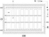
根据本发明的实施例,参考图3,金属掩模版100包括开口区O和周边区R,周边区R环绕开口区O设置,且周边区R设置有第一半刻槽101,并且,第一半刻槽101环绕开口区O设置。如此,在目前的金属掩模版的结构设计基础上,在周边区R中引入环绕开口区O的半刻设计,能够有效地改善金属掩模版100的下垂量,并降低其张网力,从而有利于提高金属掩模版100的精度。According to an embodiment of the present invention, referring to FIG. 3 , the
在本发明的一些实施例中,参考图4,第一半刻槽101到金属掩模版100的边缘在第一方向上的最小距离可以为零,第一半刻槽101到金属掩模版100的边缘在第二方向上的距离可以大于零,且第一方向与第二方向交叉设置,具体的,第一方向可以与第二方向垂直设置。如此,第一半刻槽101到金属掩模版100的边缘距离越近,对边缘区的下垂量改善越明显。In some embodiments of the present invention, referring to FIG. 4 , the minimum distance from the
根据本发明的实施例,参考图4,周边区R还可以设置有第二半刻槽102,第二半刻槽102沿第一方向延伸且设置在第一半刻槽101与开口区O之间,如此,可以进一步改善金属掩模版在第二方向上的下垂量,从而进一步提高使用该金属掩模版形成的无机封装层在不同位置的厚度均匀性。According to an embodiment of the present invention, referring to FIG. 4 , the peripheral region R may further be provided with a second half-carved
根据本发明的实施例,参考图4,开口区O可以设置有呈阵列排布的多个开口104,任意相邻两行沿第一方向排列的开口104之间还可以设置有第三半刻槽103,且第三半刻槽103是沿第一方向延伸的。如此,不仅能更进一步改善金属掩模版在第二方向上的下垂量,还可以减轻金属掩模版中间区的重量,从而进一步改善金属掩模版在第一方向上的下垂量。According to an embodiment of the present invention, referring to FIG. 4 , the opening area O may be provided with a plurality of
在本发明的一些实施例中,参考图5,第一半刻槽101在第一方向或第二方向上的宽度d1可以为6~30mm,具体例如20mm等,如此,采用上述宽度的第一半刻槽101,虽然金属掩模版的中心区下垂量基本保持不变,但是,可以显著降低边缘区的下垂量,从而使金属掩模版的整体下垂量更均匀,进而使金属掩模版形成的无机封装层的厚度渐变区范围有效缩小。In some embodiments of the present invention, referring to FIG. 5 , the width d1 of the first half-carved
在一些具体示例中,第二半刻槽102在第二方向上的宽度d2可以为6~30mm,如此,采用上述宽度的第二半刻槽102,可以更进一步降低边缘区的下垂量,从而使金属掩模版的整体下垂量更加地均匀。在另一些具体示例中,第三半刻槽103在第二方向上的宽度d3可以为5~15mm,如此,采用上述宽度的第三半刻槽103,不仅可以更进一步降低边缘区地下垂量,还可使金属掩模版在两个垂直的方向上都更均匀。In some specific examples, the width d2 of the second half-
在一些具体示例中,第一半刻槽101的深h1度可以为周边区R的厚度H的50%~60%,如此,采用上述深度的第一半刻槽101,在充分降低边缘区下垂量的同时,又不造成金属掩模版在使用时的形变。In some specific examples, the depth h1 of the first half-
在本发明的一些实施例中,参考图5,第二半刻槽102的深度h2可以大于第一半刻槽101的深度h1,如此,深度更浅的第一半刻槽101可以分散更多的内应力,从而进一步降低金属掩模版边缘区的下垂量。在一些具体示例中,第三半刻槽103的深度h3也可以与第二半刻槽102的深度h2相同,如此,开口104两侧的深度相同的半刻槽,不容易造成开口104的变形。In some embodiments of the present invention, referring to FIG. 5 , the depth h2 of the second half-
在一些具体示例中,第一半刻槽101、第二半刻槽102和第三半刻槽103,在第一方向或第二方向上的截面形状可以包括方形、倒梯形和圆形,例如图5所示的方形槽,如此,通过将各个半刻槽的截面形状设计成特定的形状,可以进一步分散应力作用下的金属掩模版的内应力,从而有效地改善金属掩模版的下垂量。In some specific examples, the cross-sectional shapes of the
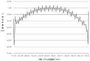
具体的,将5mm、20mm宽的第一半刻槽101与没有设置第一半刻槽101的金属掩模版进行比较,其沿第二方向的下垂量如图6所示;再将20mm宽的第一半刻槽101的金属掩模版下垂量与没有设置第一半刻槽101的金属掩模版下垂量进行差值处理,可获得如图7所示的下垂量改善量。并且,将20mm宽的第一半刻槽101与没有设置第一半刻槽101的金属掩模版进行比较,其下垂量极值对比结果如表1所示。从表1和图6、图7中都可看出,20mm宽的第一半刻槽101,可有效使金属掩模版的边缘下垂量改善在20~30微米Specifically, comparing the first half-
表1.有无第一半刻槽的金属掩模版的下垂量极值对比(单位为微米)Table 1. Comparison of extreme values of sag of metal reticle with and without the first half groove (in microns)

综上所述,根据本发明的实施例,本发明提出了一种金属掩模版,通过在周边区引入环绕开口区设置的第一半刻槽,可以有效地改善金属掩模版的下垂量,且能降低金属掩模版的张网力,从而提高使用该金属掩模版形成的无机封装层在不同位置的厚度均匀性,进而使显示面板的制作良品率更高。To sum up, according to the embodiments of the present invention, the present invention proposes a metal reticle. By introducing the first half-grooves arranged around the opening area in the peripheral area, the sag of the metal reticle can be effectively improved, and The tensioning force of the metal mask can be reduced, thereby improving the thickness uniformity of the inorganic encapsulation layer formed by using the metal mask at different positions, thereby making the production yield of the display panel higher.
在本发明的另一个方面,本发明提出了一种显示面板。根据本发明的实施例,显示面板的无机封装层,是通过上述的金属掩模版进行图案化处理的。如此,在进行图案化处理的过程中,金属掩模版由于重力作用的下垂量被有效改善,从而使图案化后的无机封装层的厚度渐变区有效地缩小,进而使显示面板的封装效果更佳。In another aspect of the present invention, the present invention provides a display panel. According to an embodiment of the present invention, the inorganic encapsulation layer of the display panel is patterned by the above-mentioned metal mask. In this way, during the patterning process, the sag of the metal mask due to the action of gravity is effectively improved, so that the thickness gradient area of the patterned inorganic encapsulation layer is effectively reduced, so that the encapsulation effect of the display panel is better. .
需要说明的是,显示面板上除了无机封装层以外,还包括必要的结构和组成,以有机发光二极管(OLED)显示面板为例,还可包括衬底、功能层结构、挡墙、有机封装层等,本领域技术人员可根据该显示面板的实际功能要求进行相应设计,在此不再赘述。It should be noted that in addition to the inorganic encapsulation layer, the display panel also includes necessary structures and compositions. Taking an organic light emitting diode (OLED) display panel as an example, it may also include a substrate, a functional layer structure, a retaining wall, and an organic encapsulation layer. etc., those skilled in the art can make corresponding designs according to the actual functional requirements of the display panel, which will not be repeated here.
综上所述,根据本发明的实施例,本发明提出了一种显示面板,其无机封装层是通过使用下垂量更小的金属掩模版进行图案化,如此,无机封装层的厚度均匀性更好,从而使显示面板的制作良品率更高。本领域技术人员能够理解的是,前面针对制作显示面板的方法所描述的特征和优点,仍适用于该显示面板,在此不再赘述。To sum up, according to the embodiments of the present invention, the present invention provides a display panel in which the inorganic encapsulation layer is patterned by using a metal mask with a smaller sag, so that the thickness uniformity of the inorganic encapsulation layer is better. good, so that the production yield of the display panel is higher. Those skilled in the art can understand that the features and advantages described above with respect to the method for manufacturing a display panel are still applicable to the display panel, and details are not repeated here.
在本发明的另一个方面,本发明提出了一种显示装置。根据本发明的实施例,显示装置包括上述的显示面板。In another aspect of the present invention, the present invention provides a display device. According to an embodiment of the present invention, a display device includes the above-mentioned display panel.
根据本发明的实施例,该显示装置的具体类型不受特别的限制,本领域内常用的显示装置的类型均可,具体例如显示屏、手机、全彩电脑或可穿戴设备等,本领域技术人员可根据显示装置的具体使用要求进行相应地选择,在此不再赘述。需要说明的是,显示装置除了上述显示面板以外,还包括其他必要的组件和结构,以OLED显示器为例,具体例如盖板、触控面板、电源和外壳等,本领域技术人员可根据显示装置的具体使用要求进行相应地补充,在此不再赘述。According to the embodiment of the present invention, the specific type of the display device is not particularly limited, and any type of display device commonly used in the art can be used, such as a display screen, a mobile phone, a full-color computer or a wearable device, etc. Personnel can make corresponding selections according to the specific usage requirements of the display device, which will not be repeated here. It should be noted that, in addition to the above-mentioned display panel, the display device also includes other necessary components and structures, taking an OLED display as an example, such as a cover plate, a touch panel, a power supply and a casing, etc., and those skilled in the art can use the display device according to the The specific use requirements of the system should be supplemented accordingly, and will not be repeated here.
综上所述,根据本发明的实施例,本发明提出了一种显示装置,其显示面板上的无机封装层的厚度均匀性更好,从而使显示面板的良品率更高,进而使该显示装置的长期使用稳定性更高。本领域技术人员能够理解的是,前面针对显示面板所描述的特征和优点,仍适用于该显示装置,在此不再赘述。To sum up, according to the embodiments of the present invention, the present invention proposes a display device in which the thickness uniformity of the inorganic encapsulation layer on the display panel is better, so that the yield rate of the display panel is higher, and the display panel is further improved. The long-term use stability of the device is higher. Those skilled in the art can understand that the features and advantages described above with respect to the display panel are still applicable to the display device, and are not repeated here.
在本发明的描述中,需要理解的是,术语“中心”、“纵向”、“横向”、“长度”、“宽度”、“厚度”、“上”、“下”、“前”、“后”、“左”、“右”、“竖直”、“水平”、“顶”、“底”、“内”、“外”、“顺时针”、“逆时针”、“轴向”、“径向”、“周向”等指示的方位或位置关系为基于附图所示的方位或位置关系,仅是为了便于描述本发明和简化描述,而不是指示或暗示所指的装置或元件必须具有特定的方位、以特定的方位构造和操作,因此不能理解为对本发明的限制。In the description of the present invention, it should be understood that the terms "center", "longitudinal", "lateral", "length", "width", "thickness", "upper", "lower", "front", " Back, Left, Right, Vertical, Horizontal, Top, Bottom, Inner, Outer, Clockwise, Counterclockwise, Axial , "radial", "circumferential" and other indicated orientations or positional relationships are based on the orientations or positional relationships shown in the accompanying drawings, and are only for the convenience of describing the present invention and simplifying the description, rather than indicating or implying the indicated device or Elements must have a particular orientation, be constructed and operate in a particular orientation and are therefore not to be construed as limitations of the invention.
在本发明的描述中,除非另有明确的规定和限定,术语“安装”、“相连”、“连接”、“固定”等术语应做广义理解,例如,可以是固定连接,也可以是可拆卸连接,或成一体;可以是机械连接,也可以是电连接;可以是直接相连,也可以通过中间媒介间接相连,可以是两个元件内部的连通或两个元件的相互作用关系。对于本领域的普通技术人员而言,可以根据具体情况理解上述术语在本发明中的具体含义。In the description of the present invention, unless otherwise expressly specified and limited, the terms "installed", "connected", "connected", "fixed" and other terms should be understood in a broad sense, for example, it may be a fixed connection or a It can be a mechanical connection or an electrical connection; it can be a direct connection or an indirect connection through an intermediate medium, and it can be the internal communication between the two elements or the interaction relationship between the two elements. For those of ordinary skill in the art, the specific meanings of the above terms in the present invention can be understood according to specific situations.
此外,术语“第一”、“第二”仅用于描述目的,而不能理解为指示或暗示相对重要性或者隐含指明所指示的技术特征的数量。由此,限定有“第一”、“第二”的特征可以明示或者隐含地包括至少一个该特征。在本发明的描述中,“多个”的含义是至少两个,例如两个,三个等,除非另有明确具体的限定。In addition, the terms "first" and "second" are only used for descriptive purposes, and should not be construed as indicating or implying relative importance or implying the number of indicated technical features. Thus, a feature delimited with "first", "second" may expressly or implicitly include at least one of that feature. In the description of the present invention, "plurality" means at least two, such as two, three, etc., unless otherwise expressly and specifically defined.
在本说明书的描述中,参考术语“一个实施例”、“一些实施例”、“示例”、“具体示例”、或“一些示例”等的描述意指结合该实施例或示例描述的具体特征、结构、材料或者特点包含于本发明的至少一个实施例或示例中。在本说明书中,对上述术语的示意性表述不必须针对的是相同的实施例或示例。而且,描述的具体特征、结构、材料或者特点可以在任一个或多个实施例或示例中以合适的方式结合。此外,在不相互矛盾的情况下,本领域的技术人员可以将本说明书中描述的不同实施例或示例以及不同实施例或示例的特征进行结合和组合。In the description of this specification, description with reference to the terms "one embodiment," "some embodiments," "example," "specific example," or "some examples", etc., mean specific features described in connection with the embodiment or example , structure, material or feature is included in at least one embodiment or example of the present invention. In this specification, schematic representations of the above terms are not necessarily directed to the same embodiment or example. Furthermore, the particular features, structures, materials or characteristics described may be combined in any suitable manner in any one or more embodiments or examples. Furthermore, those skilled in the art may combine and combine the different embodiments or examples described in this specification, as well as the features of the different embodiments or examples, without conflicting each other.
尽管上面已经示出和描述了本发明的实施例,可以理解的是,上述实施例是示例性的,不能理解为对本发明的限制,本领域的普通技术人员在本发明的范围内可以对上述实施例进行变化、修改、替换和变型。Although the embodiments of the present invention have been shown and described above, it should be understood that the above embodiments are exemplary and should not be construed as limiting the present invention. Embodiments are subject to variations, modifications, substitutions and variations.
Claims (7)
Translated fromChinesePriority Applications (2)
| Application Number | Priority Date | Filing Date | Title |
|---|---|---|---|
| CN201911172698.4ACN110838565B (en) | 2019-11-26 | 2019-11-26 | Metal mask, display panel and display device |
| US16/989,389US11545646B2 (en) | 2019-11-26 | 2020-08-10 | Metal mask having groove within peripheral region thereof, display panel and display device |
Applications Claiming Priority (1)
| Application Number | Priority Date | Filing Date | Title |
|---|---|---|---|
| CN201911172698.4ACN110838565B (en) | 2019-11-26 | 2019-11-26 | Metal mask, display panel and display device |
Publications (2)
| Publication Number | Publication Date |
|---|---|
| CN110838565A CN110838565A (en) | 2020-02-25 |
| CN110838565Btrue CN110838565B (en) | 2022-07-29 |
Family
ID=69577539
Family Applications (1)
| Application Number | Title | Priority Date | Filing Date |
|---|---|---|---|
| CN201911172698.4AActiveCN110838565B (en) | 2019-11-26 | 2019-11-26 | Metal mask, display panel and display device |
Country Status (2)
| Country | Link |
|---|---|
| US (1) | US11545646B2 (en) |
| CN (1) | CN110838565B (en) |
Families Citing this family (4)
| Publication number | Priority date | Publication date | Assignee | Title |
|---|---|---|---|---|
| US7753751B2 (en)* | 2004-09-29 | 2010-07-13 | Semiconductor Energy Laboratory Co., Ltd. | Method of fabricating the display device |
| CN111621742B (en)* | 2020-05-19 | 2021-07-23 | 武汉华星光电半导体显示技术有限公司 | Mask plate, application method thereof and preparation method of packaging layer |
| TWI798775B (en)* | 2021-07-30 | 2023-04-11 | 達運精密工業股份有限公司 | Method for manufacturing metal mask and metal mask |
| CN114540787B (en)* | 2021-11-23 | 2024-08-09 | 京东方科技集团股份有限公司 | Mask plate, manufacturing method thereof and display panel |
Citations (10)
| Publication number | Priority date | Publication date | Assignee | Title |
|---|---|---|---|---|
| JP2000096211A (en)* | 1998-09-24 | 2000-04-04 | Stanley Electric Co Ltd | Vacuum film forming mask and method for manufacturing thin film element using the same |
| JP5534093B1 (en)* | 2013-01-11 | 2014-06-25 | 大日本印刷株式会社 | Metal mask and metal mask manufacturing method |
| CN103911584A (en)* | 2012-12-31 | 2014-07-09 | 上海天马微电子有限公司 | Mask plate |
| CN106119773A (en)* | 2016-08-03 | 2016-11-16 | 京东方科技集团股份有限公司 | Mask plate and manufacture method, evaporation mask plate assembly and manufacture method thereof |
| CN106480404A (en)* | 2016-12-28 | 2017-03-08 | 京东方科技集团股份有限公司 | A kind of mask integrated framework and evaporation coating device |
| CN107675128A (en)* | 2017-11-17 | 2018-02-09 | 京东方科技集团股份有限公司 | Mask plate framework |
| CN108385083A (en)* | 2018-02-26 | 2018-08-10 | 京东方科技集团股份有限公司 | Mask plate and preparation method thereof, display panel and its packaging method, display device |
| CN109023235A (en)* | 2018-08-13 | 2018-12-18 | 京东方科技集团股份有限公司 | mask substrate, mask assembly, display panel and display device |
| CN109536886A (en)* | 2018-12-17 | 2019-03-29 | 福建华佳彩有限公司 | A kind of evaporation coating device and oled panel evaporation coating method |
| CN109913805A (en)* | 2019-03-27 | 2019-06-21 | 京东方科技集团股份有限公司 | a mask |
Family Cites Families (10)
| Publication number | Priority date | Publication date | Assignee | Title |
|---|---|---|---|---|
| JPS53570A (en) | 1976-06-25 | 1978-01-06 | Hitachi Ltd | Aligning apparatus for rod-like articles |
| JP2001185350A (en)* | 1999-12-24 | 2001-07-06 | Sanyo Electric Co Ltd | Worn mask, its manufacturing method, electroluminescent display device and its manufacturing method |
| JP2002175878A (en)* | 2000-09-28 | 2002-06-21 | Sanyo Electric Co Ltd | Layer forming method and color light emitting device manufacturing method |
| JP6078818B2 (en)* | 2013-07-02 | 2017-02-15 | 株式会社ブイ・テクノロジー | Film-forming mask and film-forming mask manufacturing method |
| CN105047829B (en)* | 2015-09-18 | 2017-05-10 | 京东方科技集团股份有限公司 | Packaging structure and packaging method of organic electroluminescent device, flexible display device |
| JP6465075B2 (en)* | 2016-05-26 | 2019-02-06 | 大日本印刷株式会社 | Vapor deposition mask, vapor deposition mask with frame, method for producing organic semiconductor element, and method for producing organic EL display |
| CN106086781B (en)* | 2016-06-15 | 2018-09-11 | 京东方科技集团股份有限公司 | Mask assembly and its manufacturing method, display device |
| JP7017032B2 (en)* | 2016-06-28 | 2022-02-08 | 大日本印刷株式会社 | A vapor deposition mask, a method for manufacturing an organic semiconductor device, and a method for manufacturing an organic EL display. |
| WO2018062300A1 (en)* | 2016-09-30 | 2018-04-05 | 大日本印刷株式会社 | Evaporation mask, evaporation mask provided with frame, evaporation mask prepared body, method for forming vapor deposition pattern, method for manufacturing organic semiconductor element, and method for manufacturing organic el display |
| CN110747431B (en)* | 2019-11-20 | 2022-04-08 | 京东方科技集团股份有限公司 | Fine mask and fabrication method thereof, combined mask and display substrate |
- 2019
- 2019-11-26CNCN201911172698.4Apatent/CN110838565B/enactiveActive
- 2020
- 2020-08-10USUS16/989,389patent/US11545646B2/enactiveActive
Patent Citations (10)
| Publication number | Priority date | Publication date | Assignee | Title |
|---|---|---|---|---|
| JP2000096211A (en)* | 1998-09-24 | 2000-04-04 | Stanley Electric Co Ltd | Vacuum film forming mask and method for manufacturing thin film element using the same |
| CN103911584A (en)* | 2012-12-31 | 2014-07-09 | 上海天马微电子有限公司 | Mask plate |
| JP5534093B1 (en)* | 2013-01-11 | 2014-06-25 | 大日本印刷株式会社 | Metal mask and metal mask manufacturing method |
| CN106119773A (en)* | 2016-08-03 | 2016-11-16 | 京东方科技集团股份有限公司 | Mask plate and manufacture method, evaporation mask plate assembly and manufacture method thereof |
| CN106480404A (en)* | 2016-12-28 | 2017-03-08 | 京东方科技集团股份有限公司 | A kind of mask integrated framework and evaporation coating device |
| CN107675128A (en)* | 2017-11-17 | 2018-02-09 | 京东方科技集团股份有限公司 | Mask plate framework |
| CN108385083A (en)* | 2018-02-26 | 2018-08-10 | 京东方科技集团股份有限公司 | Mask plate and preparation method thereof, display panel and its packaging method, display device |
| CN109023235A (en)* | 2018-08-13 | 2018-12-18 | 京东方科技集团股份有限公司 | mask substrate, mask assembly, display panel and display device |
| CN109536886A (en)* | 2018-12-17 | 2019-03-29 | 福建华佳彩有限公司 | A kind of evaporation coating device and oled panel evaporation coating method |
| CN109913805A (en)* | 2019-03-27 | 2019-06-21 | 京东方科技集团股份有限公司 | a mask |
Also Published As
| Publication number | Publication date |
|---|---|
| US11545646B2 (en) | 2023-01-03 |
| US20210159454A1 (en) | 2021-05-27 |
| CN110838565A (en) | 2020-02-25 |
Similar Documents
| Publication | Publication Date | Title |
|---|---|---|
| CN110838565B (en) | Metal mask, display panel and display device | |
| CN102569673B (en) | The method of solder mask frame assembly, its manufacture method and manufacture organic light emitting display | |
| US10934613B2 (en) | Mask plate, mask plate assembly including mask plate and method for manufacturing same | |
| CN104952884B (en) | AMOLED back board structure and preparation method thereof | |
| US20150013601A1 (en) | Mask frame assembly for thin layer deposition and organic light emitting display device | |
| US10818696B2 (en) | Display panel and fabricating method thereof | |
| CN109023235B (en) | Mask substrate, mask assembly, display panel and display device | |
| TWI618804B (en) | Mask sheet and method of manufacturing organic light emitting diode display using same | |
| CN206706184U (en) | Mask plate and mask sheet | |
| US11800780B2 (en) | Mask device and manufacturing method thereof, evaporation method and display device | |
| JP6977140B2 (en) | Mask and its manufacturing method | |
| WO2016004698A1 (en) | Oled display device and manufacturing method thereof, display device and evaporation-deposition mask plate | |
| US9891463B2 (en) | Mask for forming color filter layer, method for fabricating color filter substrate, and color filter substrate | |
| WO2020113751A1 (en) | Mask | |
| CN113403573B (en) | mask | |
| WO2020143217A1 (en) | Masking unit, and mask plate assembly provided with masking unit | |
| CN104377229A (en) | Array substrate and display device | |
| WO2019007136A1 (en) | Array substrate and preparation method therefor, and display panel | |
| WO2019033856A1 (en) | Mask plate, oled display substrate, display device, and manufacturing methods | |
| CN110098239A (en) | Dot structure, display base plate, mask plate and evaporation coating method | |
| JP2013112854A (en) | Film deposition apparatus and film deposition method | |
| WO2021238439A1 (en) | Oled display panel and manufacturing method therefor | |
| US20220064780A1 (en) | Mask assembly | |
| CN114335374A (en) | Display substrate, manufacturing method thereof and display device | |
| TW201342683A (en) | Distributor and coating device using the same |
Legal Events
| Date | Code | Title | Description |
|---|---|---|---|
| PB01 | Publication | ||
| PB01 | Publication | ||
| SE01 | Entry into force of request for substantive examination | ||
| SE01 | Entry into force of request for substantive examination | ||
| GR01 | Patent grant | ||
| GR01 | Patent grant |