CN110831300A - LED matrix dimming circuit and method and electronic equipment - Google Patents
LED matrix dimming circuit and method and electronic equipmentDownload PDFInfo
- Publication number
- CN110831300A CN110831300ACN201911354547.0ACN201911354547ACN110831300ACN 110831300 ACN110831300 ACN 110831300ACN 201911354547 ACN201911354547 ACN 201911354547ACN 110831300 ACN110831300 ACN 110831300A
- Authority
- CN
- China
- Prior art keywords
- circuit
- led matrix
- switch
- dimming
- switch tube
- Prior art date
- Legal status (The legal status is an assumption and is not a legal conclusion. Google has not performed a legal analysis and makes no representation as to the accuracy of the status listed.)
- Pending
Links
Images


Landscapes
- Circuit Arrangement For Electric Light Sources In General (AREA)
Abstract
Description
Translated fromChinese技术领域technical field
本发明涉及LED技术领域,尤其涉及一种LED矩阵调光电路、LED矩阵调光方法及电子设备。The present invention relates to the field of LED technology, in particular to an LED matrix dimming circuit, an LED matrix dimming method and electronic equipment.
背景技术Background technique
为了应对当前在显示器领域中MINI LED及Micro LED高昂的成本及复杂的驱动系统,越来越多地应用矩阵调光,然而,由于背光LED系统中存在寄生电容,当背光系统开通或者关断的瞬间由于寄生电容存储的电荷放电,背光就会出现灯光拖影(俗称鬼影)现象,这种现象对我们的观看体验和画质的提升带来了极大的困扰。In order to cope with the high cost and complex driving system of MINI LED and Micro LED in the display field, matrix dimming is increasingly applied. However, due to the parasitic capacitance in the backlight LED system, when the backlight system is turned on or off, the Instantaneously, due to the discharge of the charge stored in the parasitic capacitor, the backlight will have a phenomenon of light smear (commonly known as ghosting), which brings great trouble to our viewing experience and the improvement of image quality.
发明内容SUMMARY OF THE INVENTION
本发明的主要目的在于提出一种LED矩阵调光电路、LED矩阵调光方法及电子设备,旨在解决现有技术中LED显示器出现灯光拖影的问题。The main purpose of the present invention is to provide an LED matrix dimming circuit, an LED matrix dimming method and an electronic device, aiming at solving the problem of light smear in the LED display in the prior art.
为实现上述目的,本发明提供一种LED矩阵调光电路,所述LED矩阵调光电路包括控制电路、开关电路、LED矩阵电路、调光电路以及预充电电路,其中:In order to achieve the above object, the present invention provides an LED matrix dimming circuit, the LED matrix dimming circuit includes a control circuit, a switch circuit, an LED matrix circuit, a dimming circuit and a pre-charging circuit, wherein:
所述控制电路,用于对应输出第一电平信号和第二电平信号至所述开关电路以及所述预充电电路,以控制所述开关电路关断时预充电电路导通;the control circuit, for correspondingly outputting the first level signal and the second level signal to the switch circuit and the precharge circuit, so as to control the precharge circuit to be turned on when the switch circuit is turned off;
所述预充电电路,与所述LED矩阵电路的输出端连接,用于在所述开关电路关断时,输出充电电压;the precharge circuit, connected to the output end of the LED matrix circuit, is used for outputting a charging voltage when the switch circuit is turned off;
所述调光电路,与所述LED矩阵电路的输出端连接,用于接收所述控制电路的驱动信号以调节背光电流。The dimming circuit is connected to the output end of the LED matrix circuit, and is used for receiving the driving signal of the control circuit to adjust the backlight current.
可选地,所述LED矩阵调光电路还包括放电电路;Optionally, the LED matrix dimming circuit further includes a discharge circuit;
所述控制电路,还用于输出第一电平信号至所述放电电路,以控制所述开关电路关断时放电电路导通;The control circuit is further configured to output a first level signal to the discharge circuit, so as to control the discharge circuit to be turned on when the switch circuit is turned off;
所述放电电路,与所述LED矩阵电路的输入端连接,用于在所述开关电路关断时,对所述LED矩阵电路进行放电。The discharge circuit is connected to the input end of the LED matrix circuit, and is used for discharging the LED matrix circuit when the switch circuit is turned off.
可选地,所述放电电路包括多个放电单元,每个放电单元与所述LED矩阵电路的一LED单元行的输入端连接;Optionally, the discharge circuit includes a plurality of discharge units, and each discharge unit is connected to an input end of a row of LED units of the LED matrix circuit;
每个放电单元包括第一开关管、第一电阻以及第二电阻;所述第一开关管的受控端分别连接第一电阻的第一端以及所述控制电路,所述第一电阻的第二端连接第一电源,所述第一开关管的电源端通过第二电阻与对应LED单元行的输入端连接,所述第一开关管的输出端接地。Each discharge unit includes a first switch tube, a first resistor and a second resistor; the controlled end of the first switch tube is respectively connected to the first end of the first resistor and the control circuit, and the first end of the first resistor is connected to the control circuit. The two terminals are connected to the first power supply, the power supply terminal of the first switch tube is connected to the input terminal of the corresponding LED unit row through the second resistor, and the output terminal of the first switch tube is grounded.
可选地,所述预充电电路包括多个预充电单元,每个预充电单元与所述LED矩阵电路的一LED单元列的输出端连接;Optionally, the precharge circuit includes a plurality of precharge units, and each precharge unit is connected to an output end of an LED unit column of the LED matrix circuit;
每个预充电单元包括第二开关管、第三电阻以及第四电阻;所述第二开关管的输出端连接对应LED单元列的输出端,所述第二开关管的受控端通过第三电阻与控制电路连接,所述第二开关管的电源端连接第二电源;所述第四电阻设置在所述第二开关管的电源端及受控端之间。Each precharge unit includes a second switch tube, a third resistor and a fourth resistor; the output end of the second switch tube is connected to the output end of the corresponding LED unit column, and the controlled end of the second switch tube is connected to the output end of the second switch tube through the third The resistor is connected to the control circuit, and the power terminal of the second switch tube is connected to the second power source; the fourth resistor is arranged between the power terminal and the controlled terminal of the second switch tube.
可选地,所述开关电路包括多个开关单元,每个开关单元与所述LED矩阵电路的一LED单元行的输入端连接;Optionally, the switch circuit includes a plurality of switch units, and each switch unit is connected to an input end of a row of LED units of the LED matrix circuit;
每个开关单元包括:第三开关管以及第五电阻;所述第三开关管的输出端与对应LED单元行的输入端连接,所述第三开关管的受控端连接所述控制电路,所述第三开关管的电源端连接第三电源;所述第五电阻设置在所述第三开关管的电源端及控制端之间。Each switch unit includes: a third switch tube and a fifth resistor; the output end of the third switch tube is connected to the input end of the corresponding LED unit row, and the controlled end of the third switch tube is connected to the control circuit, The power supply terminal of the third switch tube is connected to the third power supply; the fifth resistor is arranged between the power supply terminal and the control terminal of the third switch tube.
可选地,所述调光电路包括多个调光单元,每个调光单元与所述LED矩阵电路的一LED单元列的输出端连接,每个调光单元包括第四开关管;Optionally, the dimming circuit includes a plurality of dimming units, each dimming unit is connected to an output end of an LED unit column of the LED matrix circuit, and each dimming unit includes a fourth switch tube;
所述第四开关管的输入端连接对应LED矩阵电路单元列的输出端,所述第四开关管的受控端连接所述控制电路,所述第四开关管的输出端接地。The input end of the fourth switch tube is connected to the output end of the corresponding LED matrix circuit unit column, the controlled end of the fourth switch tube is connected to the control circuit, and the output end of the fourth switch tube is grounded.
可选地,所述第二开关管、第三开关管以及第四开关管为三极管或MOS管。Optionally, the second switch transistor, the third switch transistor and the fourth switch transistor are triode transistors or MOS transistors.
此外,为实现上述目的,本发明还提供一种LED矩阵调光方法,所述方法包括:In addition, in order to achieve the above object, the present invention also provides an LED matrix dimming method, the method comprising:
对应输出第一电平信号和第二电平信号至开关电路以及预充电电路,以控制所述预充电电路在所述开关电路关断时输出充电电压至连接的LED矩阵电路的输出端。Correspondingly output the first level signal and the second level signal to the switch circuit and the precharge circuit, so as to control the precharge circuit to output a charging voltage to the output terminal of the connected LED matrix circuit when the switch circuit is turned off.
可选地,所述方法还包括:Optionally, the method further includes:
发送第一电平信号至放电电路,以使所述放电电路在所述开关电路关断之后对所述LED矩阵电路的输入端进行放电。A first level signal is sent to the discharge circuit, so that the discharge circuit discharges the input terminal of the LED matrix circuit after the switch circuit is turned off.
此外,为实现上述目的,本发明还提供一种电子设备,所述电子设备包括LED矩阵调光电路,所述LED矩阵调光电路被配置为如上所述的LED矩阵调光电路或者应用于如上所述的LED矩阵调光方法。In addition, in order to achieve the above object, the present invention also provides an electronic device, the electronic device includes an LED matrix dimming circuit, and the LED matrix dimming circuit is configured as the above LED matrix dimming circuit or applied to the above The described LED matrix dimming method.
本发明实施例在所述LED矩阵调光电路设置有控制电路、开关电路、LED矩阵电路、调光电路以及预充电电路,其中:所述控制电路,用于对应输出第一电平信号和第二电平信号至所述开关电路以及所述预充电电路,以控制所述开关电路关断时预充电电路导通;所述预充电电路,与所述LED矩阵电路的输出端连接,用于在所述开关电路关断时,输出充电电压;所述调光电路,与所述LED矩阵电路的输出端连接,用于接收所述控制电路的驱动信号以调节背光电流。其中通过设置预充电电路,在开关电路阻断时,迅速提升LED矩阵电路的负端电压,使对应LED压差低于启动电压,以迅速关断LED,避免出现灯光拖影。In the embodiment of the present invention, the LED matrix dimming circuit is provided with a control circuit, a switch circuit, an LED matrix circuit, a dimming circuit and a precharge circuit, wherein: the control circuit is used for correspondingly outputting the first level signal and the second level signal. A two-level signal is sent to the switch circuit and the precharge circuit to control the precharge circuit to be turned on when the switch circuit is turned off; the precharge circuit is connected to the output end of the LED matrix circuit for When the switch circuit is turned off, the charging voltage is output; the dimming circuit is connected to the output end of the LED matrix circuit, and is used for receiving the driving signal of the control circuit to adjust the backlight current. Among them, by setting a pre-charging circuit, when the switching circuit is blocked, the negative terminal voltage of the LED matrix circuit is rapidly increased, so that the corresponding LED voltage difference is lower than the starting voltage, so as to quickly turn off the LED and avoid light smearing.
附图说明Description of drawings
为了更清楚地说明本发明实施例或现有技术中的技术方案,下面将对实施例或现有技术描述中所需要使用的附图作简单地介绍,显而易见地,下面描述中的附图仅仅是本发明的一些实施例,对于本领域普通技术人员来讲,在不付出创造性劳动的前提下,还可以根据这些附图示出的结构获得其他的附图。In order to explain the embodiments of the present invention or the technical solutions in the prior art more clearly, the following briefly introduces the accompanying drawings that need to be used in the description of the embodiments or the prior art. Obviously, the accompanying drawings in the following description are only These are some embodiments of the present invention, and for those of ordinary skill in the art, other drawings can also be obtained according to the structures shown in these drawings without creative efforts.
图1为本发明LED矩阵调光电路一实施例的功能模块图;FIG. 1 is a functional block diagram of an embodiment of an LED matrix dimming circuit of the present invention;
图2为本发明LED矩阵调光电路另一实施例的功能模块图;FIG. 2 is a functional block diagram of another embodiment of the LED matrix dimming circuit of the present invention;
图3为本发明LED矩阵调光电路应用在图2实施例中的电路结构图。FIG. 3 is a circuit structure diagram of the LED matrix dimming circuit of the present invention applied in the embodiment of FIG. 2 .
本发明目的的实现、功能特点及优点将结合实施例,参照附图做进一步说明。The realization, functional characteristics and advantages of the present invention will be further described with reference to the accompanying drawings in conjunction with the embodiments.
附图标号说明:Description of reference numbers:


具体实施方式Detailed ways
应当理解,此处所描述的具体实施例仅仅用以解释本发明,并不用于限定本发明。It should be understood that the specific embodiments described herein are only used to explain the present invention, but not to limit the present invention.
下面将结合本发明实施例中的附图,对本发明实施例中的技术方案进行清楚、完整地描述,显然,所描述的实施例仅仅是本发明的一部分实施例,而不是全部的实施例。基于本发明中的实施例,本领域普通技术人员在没有作出创造性劳动前提下所获得的所有其他实施例,都属于本发明保护的范围。The technical solutions in the embodiments of the present invention will be clearly and completely described below with reference to the accompanying drawings in the embodiments of the present invention. Obviously, the described embodiments are only a part of the embodiments of the present invention, not all of the embodiments. Based on the embodiments of the present invention, all other embodiments obtained by those of ordinary skill in the art without creative efforts shall fall within the protection scope of the present invention.
需要说明,本发明实施例中所有方向性指示(诸如上、下、左、右、前、后......)仅用于解释在某一特定姿态(如附图所示)下各部件之间的相对位置关系、运动情况等,如果该特定姿态发生改变时,则该方向性指示也相应地随之改变。It should be noted that all directional indications (such as up, down, left, right, front, back...) in the embodiments of the present invention are only used to explain the The relative positional relationship between the components, the movement situation, etc., if the specific posture changes, the directional indication also changes accordingly.
另外,在本发明中涉及“第一”、“第二”等的描述仅用于描述目的,而不能理解为指示或暗示其相对重要性或者隐含指明所指示的技术特征的数量。由此,限定有“第一”、“第二”的特征可以明示或者隐含地包括至少一个该特征。另外,各个实施例之间的技术方案可以相互结合,但是必须是以本领域普通技术人员能够实现为基础,当技术方案的结合出现相互矛盾或无法实现时应当认为这种技术方案的结合不存在,也不在本发明要求的保护范围之内。In addition, the descriptions involving "first", "second", etc. in the present invention are only for descriptive purposes, and should not be understood as indicating or implying their relative importance or implying the number of indicated technical features. Thus, a feature delimited with "first", "second" may expressly or implicitly include at least one of that feature. In addition, the technical solutions between the various embodiments can be combined with each other, but must be based on the realization by those of ordinary skill in the art. When the combination of technical solutions is contradictory or cannot be realized, it should be considered that the combination of such technical solutions does not exist. , is not within the scope of protection required by the present invention.
本发明提供一种LED矩阵调光电路,应用于电子设备中,该电子设备可以是洗衣机、微波炉以及电视机等,请参见图1,图1为本发明LED矩阵调光电路一实施例的功能模块图。在该实施例中,所述LED矩阵调光电路包括控制电路100、开关电路200、LED矩阵电路400、调光电路500以及预充电电路300;所述控制电路100的输出端分别与开关电路200、预充电电路300及调光电路500连接,所述开关电路200的输出端与LED矩阵电路400的输入端连接,所述LED矩阵电路400的输出端分别与预充电电路300及调光电路500连接。其中:The present invention provides an LED matrix dimming circuit, which is applied to electronic equipment. The electronic equipment can be a washing machine, a microwave oven, a TV, etc. Please refer to FIG. 1 , which shows the functions of an embodiment of the LED matrix dimming circuit of the present invention. Module diagram. In this embodiment, the LED matrix dimming circuit includes a
所述控制电路100,用于对应输出第一电平信号和第二电平信号G_L至所述开关电路200以及所述预充电电路300,以控制所述开关电路200关断时预充电电路300导通;The
所述预充电电路300,与所述LED矩阵电路400的输出端连接,用于在所述开关电路200关断时,输出充电电压;The
所述调光电路500,与所述LED矩阵电路400的输出端连接,用于接收所述控制电路100的驱动信号以调节背光电流。The
上述第一电平信号和第二电平信号G_L的状态相反。当上述开关电路200接收到的来自所述控制电路100发送的第一电平信号为低电平时,输出电压至LED矩阵电路400的输入端,此时第二电平信号G_L为高电平;当上述预充电电路300接收到来自所述控制电路100发送的第二电平信号G_L为低电平时,输出电压至LED矩阵电路400的输出端,此时第一电平信号为高电平。上述调光电路500用于在根据来自所述控制电路100发送的驱动信号调节背光电流。本实施例通过设置预充电电路300,在开关电路200阻断时,迅速提升LED矩阵电路400的负端电压,使对应LED电压差低于启动电压,以迅速关断LED,避免出现灯光拖影。The states of the first level signal and the second level signal G_L are opposite. When the first level signal received by the
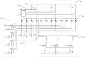
进一步地,请一并参见图2与图3,在另一实施例中,所述LED矩阵调光电路还包括放电电路600;所述放电电路600的受控端与所述控制电路100连接,所述放电电路600的电源端与所述LED矩阵电路400的输入端连接。所述放电电路600用于在接收到来自所述控制电路100发送的第一电平信号为高电平时,对所述LED矩阵电路400进行放电。即所述开关电路200与放电电路600同时接收来自控制电路100的第一电平信号,当上述开关电路200接收到来自控制电路100发送的第一电平信号为低电平时,输出电压值至LED矩阵电路400的输入端,此时放电电路600处于关断状态。当上述开关电路200接收到来自控制电路100发送的第一电平信号为高电平时,开关电路处于关断状态,上述放电电路600导通,将所述LED矩阵电路400中残留的电荷放掉。本实施例通过设置放电电路600,在开关电路200关断时,迅速放掉LED矩阵电路中的残留电荷,使对应LED正极无电压,以迅速关断LED,避免出现灯光拖影。同时放电电路600和预充电电路300结合设置,能够更好地保障显示效果。Further, please refer to FIG. 2 and FIG. 3 together, in another embodiment, the LED matrix dimming circuit further includes a
其中,所述放电电路600包括多个放电单元(未标示),每个放电单元与所述LED矩阵电路400的一LED单元行(未标示)的输入端连接;每个放电单元包括第一开关管Q1、第一电阻R1以及第二电阻R2;所述第一开关管Q1的受控端分别连接第一电阻R1的第一端以及所述控制电路100,所述第一电阻R1的第二端连接第一电源3.3V,所述第一开关管Q1的电源端通过第二电阻R2与对应LED单元行的输入端连接,所述第一开关管Q1的输出端接地。The
所述预充电电路300包括多个预充电单元(未标示),每个预充电单元与所述LED矩阵电路400的一LED单元列(未标示)的输出端连接;每个预充电单元包括第二开关管Q2、第三电阻R3以及第四电阻R4;所述第二开关管Q2的输出端连接对应LED单元列的输出端,所述第二开关管Q2的受控端通过第三电阻R3与控制电路连接,所述第二开关管Q2的电源端连接第二电源VLED+;第四电阻R4设置在所述第二开关管Q2的电源端及受控端之间。The
当所述第一开关管Q1关断时,预充电电路300接受的第二电平信号G_L变为低电平,此时第二开关管Q2导通,第二开关管Q2给LED矩阵电路400提供电压,以使得连接的LED单元列的LED负极电压升高,以至于该LED正负极电压差小于LED点亮电压,能够迅速关断,避免灯光拖影。When the first switch transistor Q1 is turned off, the second level signal G_L received by the
进一步地,所述开关电路200包括多个开关单元(未标示),每个开关单元与所述LED矩阵电路400的一LED单元行的输入端连接;每个开关单元包括:第三开关管Q3以及第五电阻R5;所述第三开关管Q3的输出端与对应LED单元行的输入端连接,所述第三开关管Q3的受控端连接所述控制电路,所述第三开关管Q3的电源端连接第三电源VBUS;第五电阻R5设置在所述第三开关管Q3的电源端及控制端之间。所述调光电路500包括多个调光单元(未标示),每个调光单元与所述LED矩阵电路400的一LED单元列的输出端连接,每个调光单元包括第四开关管Q4;所述第四开关管Q4的输入端连接对应LED矩阵电路单元列的输出端,所述第四开关管Q4的受控端连接所述控制电路,所述第四开关管Q4的输出端接地。Further, the
所述开关电路200中的每个开关单元的第三开关管Q3依次分时错相导通,通过调节所述调光电路500中的调光单元的第四开关管Q4的占空比来调节背光电流,一次实现LED背光系统的矩阵调光(分时调节),例如,当处于第一导通优先级的第三开关管Q3接收到低电平信号导通的同时,第四开关管Q4接收到高点平信号关断,则LED单元列A中A1点亮,当下一个场同步信号周期到来,处于第一导通优先级的第三开关管Q3接收到高电平信号而关断,处于第二导通优先级的第三开关管Q3接收到低电平信号导通,则LED单元列A中A2点亮。通过在每行设置开关电路及在每列设置调光电路来对所有LED的开关进行控制,无需为每个LED设置独立开关,节省了成本。The third switch transistor Q3 of each switch unit in the
其中,上述开关管可以为三极管;具体地,所述第四开关管Q4为PNP型三极管,第四开关管的受控端、输入端及输出端分别对应三极管的基极、发射极及集电极;所述第二开关管Q2与第三开关管Q3为NPN型三极管,上述第二开关管Q2和第三开关管Q3的受控端、电源端及控制端分别对应三极管的基极、集电极及发射极。所述第一开关管Q1为三极管时为PNP型三极管,第一开关管Q1的受控端、电源端及输出端分别对应三极管的基极、发射极及集电极。Wherein, the above-mentioned switch tube may be a triode; specifically, the fourth switch tube Q4 is a PNP type triode, and the controlled end, the input end and the output end of the fourth switch tube correspond to the base, emitter and collector of the triode respectively The second switch tube Q2 and the third switch tube Q3 are NPN type triodes, and the controlled end, the power supply end and the control end of the above-mentioned second switch tube Q2 and the third switch tube Q3 correspond to the base and collector of the triode respectively. and emitter. When the first switch Q1 is a triode, it is a PNP type triode, and the controlled terminal, the power terminal and the output terminal of the first switch Q1 correspond to the base, emitter and collector of the triode respectively.
上述开关管也可以任一个为MOS管。当第四开关管为MOS管时,所述第四开关管Q4为PMOS管,第四开关管Q4的受控端、输入端及输出端分别对应PMOS管的源极、栅极及漏极;所述第二开关管Q2与第三开关管Q3为MOS管时为NMOS管,上述第二开关管Q2和第三开关管Q3的受控端、电源端及控制端分别对应MOS管的源极、漏极及栅极。所述第一开关管Q1为MOS管时为PMOS管,第一开关管Q1的受控端、电源端及输出端分别对应MOS管的源极、栅极及漏极。本方案提供了多种可供选择的开关控制方案,相比集成芯片,节约了成本,同时与LED矩阵电路对应分布,结构排布合理。Any one of the above-mentioned switch tubes can also be a MOS tube. When the fourth switch tube is a MOS tube, the fourth switch tube Q4 is a PMOS tube, and the controlled end, the input end and the output end of the fourth switch tube Q4 correspond to the source, gate and drain of the PMOS tube respectively; When the second switch transistor Q2 and the third switch transistor Q3 are MOS transistors, they are NMOS transistors, and the controlled terminal, the power supply terminal and the control terminal of the second switch transistor Q2 and the third switch transistor Q3 respectively correspond to the source electrodes of the MOS transistors. , drain and gate. When the first switch transistor Q1 is a MOS transistor, it is a PMOS transistor, and the controlled terminal, the power terminal and the output terminal of the first switch transistor Q1 correspond to the source, gate and drain of the MOS transistor, respectively. This solution provides a variety of switch control solutions to choose from. Compared with integrated chips, the cost is saved. At the same time, it is distributed corresponding to the LED matrix circuit, and the structure is arranged reasonably.
此外,本发明还保护一种LED矩阵调光方法,所述方法包括:In addition, the present invention also protects an LED matrix dimming method, the method comprising:
步骤S10,对应输出第一电平信号和第二电平信号至开关电路以及预充电电路,以控制所述预充电电路在所述开关电路关断时输出充电电压至连接的LED矩阵电路的输出端。Step S10, correspondingly output the first level signal and the second level signal to the switch circuit and the precharge circuit, so as to control the precharge circuit to output a charging voltage to the output of the connected LED matrix circuit when the switch circuit is turned off end.
进一步地,所述方法还包括:Further, the method also includes:
步骤S20,发送第一电平信号至放电电路,以使所述放电电路在所述开关电路关断之后对所述LED矩阵电路的输入端进行放电。Step S20, sending a first level signal to the discharge circuit, so that the discharge circuit discharges the input end of the LED matrix circuit after the switch circuit is turned off.
本方法应用于LED矩阵调光电路,该LED矩阵调光电路的结构可参照上述实施例,在此不再赘述。其实现过程与前述结构实施例一致,可以参照执行。The method is applied to an LED matrix dimming circuit, and the structure of the LED matrix dimming circuit can be referred to the above-mentioned embodiments, which will not be repeated here. The implementation process thereof is consistent with the foregoing structural embodiments, and can be executed with reference.
本发明还保护一种电子设备,该电子设备包括LED矩阵调光电路,该LED矩阵调光电路的结构可参照上述实施例,在此不再赘述。理所应当地,由于本实施例的保护装置采用了上述LED矩阵调光电路的技术方案,因此该保护装置具有上述LED矩阵调光电路所有的有益效果。The present invention also protects an electronic device, the electronic device includes an LED matrix dimming circuit, and the structure of the LED matrix dimming circuit can be referred to the above-mentioned embodiments, which will not be repeated here. As a matter of course, since the protection device of this embodiment adopts the technical solution of the above-mentioned LED matrix dimming circuit, the protection device has all the beneficial effects of the above-mentioned LED matrix dimming circuit.
需要说明的是,在本文中,术语“包括”、“包含”或者其任何其他变体意在涵盖非排他性的包含,从而使得包括一系列要素的过程、方法、物品或者系统不仅包括那些要素,而且还包括没有明确列出的其他要素,或者是还包括为这种过程、方法、物品或者系统所固有的要素。在没有更多限制的情况下,由语句“包括一个......”限定的要素,并不排除在包括该要素的过程、方法、物品或者系统中还存在另外的相同要素。上述本发明实施例序号仅仅为了描述,不代表实施例的优劣。It should be noted that, herein, the terms "comprising", "comprising" or any other variation thereof are intended to encompass non-exclusive inclusion, such that a process, method, article or system comprising a series of elements includes not only those elements, It also includes other elements not expressly listed or inherent to such a process, method, article or system. Without further limitation, an element qualified by the phrase "comprising a..." does not preclude the presence of additional identical elements in the process, method, article or system that includes the element. The above-mentioned serial numbers of the embodiments of the present invention are only for description, and do not represent the advantages or disadvantages of the embodiments.
以上仅为本发明的优选实施例,并非因此限制本发明的专利范围,凡是利用本发明说明书及附图内容所作的等效结构或等效流程变换,或直接或间接运用在其他相关的技术领域,均同理包括在本发明的专利保护范围内。The above are only preferred embodiments of the present invention, and are not intended to limit the scope of the present invention. Any equivalent structure or equivalent process transformation made by using the contents of the description and drawings of the present invention, or directly or indirectly applied in other related technical fields , are similarly included in the scope of patent protection of the present invention.
Claims (10)
Translated fromChinesePriority Applications (1)
| Application Number | Priority Date | Filing Date | Title |
|---|---|---|---|
| CN201911354547.0ACN110831300A (en) | 2019-12-24 | 2019-12-24 | LED matrix dimming circuit and method and electronic equipment |
Applications Claiming Priority (1)
| Application Number | Priority Date | Filing Date | Title |
|---|---|---|---|
| CN201911354547.0ACN110831300A (en) | 2019-12-24 | 2019-12-24 | LED matrix dimming circuit and method and electronic equipment |
Publications (1)
| Publication Number | Publication Date |
|---|---|
| CN110831300Atrue CN110831300A (en) | 2020-02-21 |
Family
ID=69546273
Family Applications (1)
| Application Number | Title | Priority Date | Filing Date |
|---|---|---|---|
| CN201911354547.0APendingCN110831300A (en) | 2019-12-24 | 2019-12-24 | LED matrix dimming circuit and method and electronic equipment |
Country Status (1)
| Country | Link |
|---|---|
| CN (1) | CN110831300A (en) |
Cited By (4)
| Publication number | Priority date | Publication date | Assignee | Title |
|---|---|---|---|---|
| WO2021174805A1 (en)* | 2020-03-04 | 2021-09-10 | 深圳创维-Rgb电子有限公司 | Mini-led light source and driving circuit and driving method therefor |
| CN113490307A (en)* | 2021-09-06 | 2021-10-08 | 成都利普芯微电子有限公司 | Control circuit of LED display screen pre-charging circuit and pre-charging circuit |
| US11538427B1 (en) | 2022-01-07 | 2022-12-27 | Stmicroelectronics S.R.L. | High efficiency ghost illumination cancelation in emissive and non-emissive display panels |
| US11978416B2 (en) | 2022-01-07 | 2024-05-07 | Stmicroelectronics S.R.L. | High efficiency ghost illumination cancelation in emissive and non-emissive display panels |
Citations (6)
| Publication number | Priority date | Publication date | Assignee | Title |
|---|---|---|---|---|
| JPH11311970A (en)* | 1998-04-30 | 1999-11-09 | Sony Corp | Matrix driving method for current type display elements and matrix driving device for current type display elements |
| US20040041760A1 (en)* | 2002-08-30 | 2004-03-04 | Makoto Tsumura | Liquid crystal display |
| US20080231199A1 (en)* | 2007-03-20 | 2008-09-25 | Sony Corporation | Driving method for organic electroluminescence light emitting section |
| CN103680406A (en)* | 2013-12-12 | 2014-03-26 | 京东方科技集团股份有限公司 | Pixel circuit, driving method thereof and display device |
| CN104091568A (en)* | 2014-07-31 | 2014-10-08 | 无锡力芯微电子股份有限公司 | Light-emitting diode (LED) display system capable of eliminating residual shadow of LED display screen, and line scanning circuit of system |
| CN104091569A (en)* | 2014-07-31 | 2014-10-08 | 无锡力芯微电子股份有限公司 | LED display system capable of eliminating ghosting image on LED display screen and driving circuit thereof |
- 2019
- 2019-12-24CNCN201911354547.0Apatent/CN110831300A/enactivePending
Patent Citations (6)
| Publication number | Priority date | Publication date | Assignee | Title |
|---|---|---|---|---|
| JPH11311970A (en)* | 1998-04-30 | 1999-11-09 | Sony Corp | Matrix driving method for current type display elements and matrix driving device for current type display elements |
| US20040041760A1 (en)* | 2002-08-30 | 2004-03-04 | Makoto Tsumura | Liquid crystal display |
| US20080231199A1 (en)* | 2007-03-20 | 2008-09-25 | Sony Corporation | Driving method for organic electroluminescence light emitting section |
| CN103680406A (en)* | 2013-12-12 | 2014-03-26 | 京东方科技集团股份有限公司 | Pixel circuit, driving method thereof and display device |
| CN104091568A (en)* | 2014-07-31 | 2014-10-08 | 无锡力芯微电子股份有限公司 | Light-emitting diode (LED) display system capable of eliminating residual shadow of LED display screen, and line scanning circuit of system |
| CN104091569A (en)* | 2014-07-31 | 2014-10-08 | 无锡力芯微电子股份有限公司 | LED display system capable of eliminating ghosting image on LED display screen and driving circuit thereof |
Non-Patent Citations (1)
| Title |
|---|
| ——2014广州LED展的启示 蔡宗达: "小点间距显示屏常见问题与驱动芯片解决方案——2014广州LED展的启示", 《电子科学技术》* |
Cited By (4)
| Publication number | Priority date | Publication date | Assignee | Title |
|---|---|---|---|---|
| WO2021174805A1 (en)* | 2020-03-04 | 2021-09-10 | 深圳创维-Rgb电子有限公司 | Mini-led light source and driving circuit and driving method therefor |
| CN113490307A (en)* | 2021-09-06 | 2021-10-08 | 成都利普芯微电子有限公司 | Control circuit of LED display screen pre-charging circuit and pre-charging circuit |
| US11538427B1 (en) | 2022-01-07 | 2022-12-27 | Stmicroelectronics S.R.L. | High efficiency ghost illumination cancelation in emissive and non-emissive display panels |
| US11978416B2 (en) | 2022-01-07 | 2024-05-07 | Stmicroelectronics S.R.L. | High efficiency ghost illumination cancelation in emissive and non-emissive display panels |
Similar Documents
| Publication | Publication Date | Title |
|---|---|---|
| CN110831300A (en) | LED matrix dimming circuit and method and electronic equipment | |
| JP7114461B2 (en) | Pixel circuit, display panel, and driving method | |
| US10902811B2 (en) | Shift register, GOA circuit, display device and driving method | |
| US10490149B2 (en) | Discharging circuit and driving method thereof, display device | |
| CN111477162B (en) | Pixel circuit and driving method thereof, and display device | |
| US8624524B2 (en) | Power management and control module and liquid crystal display device | |
| US9830874B2 (en) | Electronic device having smaller number of drive chips | |
| CN104835531B (en) | A kind of shift register cell and its driving method, shift register and display device | |
| US10217422B2 (en) | Array substrate, driving method thereof and electronic paper | |
| KR20080111233A (en) | Driving device of liquid crystal display and liquid crystal display including the same | |
| US7489758B2 (en) | Shift register apparatus and shift register thereof | |
| WO2018040405A1 (en) | Starting voltage generating apparatus for gate electrode of liquid crystal display device | |
| CN112086071A (en) | Display panel, driving method thereof and display device | |
| US11367469B2 (en) | Shift register unit circuit and driving method, shift register, gate drive circuit, and display apparatus | |
| US7719510B2 (en) | Flat panel display, display driving apparatus thereof and shift register thereof | |
| CN115578965A (en) | A shift register circuit, display panel and display device | |
| CN108230989B (en) | Gate drive circuit and its output module, display panel | |
| US20200043431A1 (en) | Goa circuit and liquid crystal display device | |
| CN110689839A (en) | Shifting register unit, driving method, grid driving circuit and display device | |
| CN114360429A (en) | Drive circuit and display device | |
| TWI699744B (en) | Driving method, shift register, and display device using the same | |
| US20110227959A1 (en) | Liquid crystal display and data driving device | |
| CN116110327B (en) | LED driver chip and LED display | |
| CN116798344A (en) | Signal driving circuit and driving method thereof, display panel and display device | |
| CN110880285A (en) | Shift register, grid drive circuit and display panel |
Legal Events
| Date | Code | Title | Description |
|---|---|---|---|
| PB01 | Publication | ||
| PB01 | Publication | ||
| SE01 | Entry into force of request for substantive examination | ||
| SE01 | Entry into force of request for substantive examination | ||
| RJ01 | Rejection of invention patent application after publication | Application publication date:20200221 | |
| RJ01 | Rejection of invention patent application after publication |