CN110829827A - CRM boost-buck PFC converter with constant switching frequency - Google Patents
CRM boost-buck PFC converter with constant switching frequencyDownload PDFInfo
- Publication number
- CN110829827A CN110829827ACN201810889244.8ACN201810889244ACN110829827ACN 110829827 ACN110829827 ACN 110829827ACN 201810889244 ACN201810889244 ACN 201810889244ACN 110829827 ACN110829827 ACN 110829827A
- Authority
- CN
- China
- Prior art keywords
- circuit
- resistor
- output
- operational amplifier
- input
- Prior art date
- Legal status (The legal status is an assumption and is not a legal conclusion. Google has not performed a legal analysis and makes no representation as to the accuracy of the status listed.)
- Pending
Links
- 238000004804windingMethods0.000claimsabstractdescription34
- 230000007274generation of a signal involved in cell-cell signalingEffects0.000claimsabstractdescription8
- 239000003990capacitorSubstances0.000claimsdescription29
- 238000005070samplingMethods0.000claimsdescription13
- 238000001514detection methodMethods0.000claimsdescription9
- 238000000034methodMethods0.000claimsdescription3
- NTSBMKIZRSBFTA-AIDOXSFESA-NDigoxigenin bisdigitoxosideChemical groupC1[C@H](O)[C@H](O)[C@@H](C)O[C@H]1O[C@@H]1[C@@H](C)O[C@@H](O[C@@H]2C[C@@H]3[C@]([C@@H]4[C@H]([C@]5(CC[C@@H]([C@@]5(C)[C@H](O)C4)C=4COC(=O)C=4)O)CC3)(C)CC2)C[C@@H]1ONTSBMKIZRSBFTA-AIDOXSFESA-N0.000claims1
- 238000010586diagramMethods0.000description7
- 238000000354decomposition reactionMethods0.000description2
- 238000004146energy storageMethods0.000description2
- NAWXUBYGYWOOIX-SFHVURJKSA-N(2s)-2-[[4-[2-(2,4-diaminoquinazolin-6-yl)ethyl]benzoyl]amino]-4-methylidenepentanedioic acidChemical compoundC1=CC2=NC(N)=NC(N)=C2C=C1CCC1=CC=C(C(=O)N[C@@H](CC(=C)C(O)=O)C(O)=O)C=C1NAWXUBYGYWOOIX-SFHVURJKSA-N0.000description1
- TVEXGJYMHHTVKP-UHFFFAOYSA-N6-oxabicyclo[3.2.1]oct-3-en-7-oneChemical compoundC1C2C(=O)OC1C=CC2TVEXGJYMHHTVKP-UHFFFAOYSA-N0.000description1
- 238000006243chemical reactionMethods0.000description1
- 238000011217control strategyMethods0.000description1
- 238000005516engineering processMethods0.000description1
Images


Classifications
- H—ELECTRICITY
- H02—GENERATION; CONVERSION OR DISTRIBUTION OF ELECTRIC POWER
- H02M—APPARATUS FOR CONVERSION BETWEEN AC AND AC, BETWEEN AC AND DC, OR BETWEEN DC AND DC, AND FOR USE WITH MAINS OR SIMILAR POWER SUPPLY SYSTEMS; CONVERSION OF DC OR AC INPUT POWER INTO SURGE OUTPUT POWER; CONTROL OR REGULATION THEREOF
- H02M1/00—Details of apparatus for conversion
- H02M1/44—Circuits or arrangements for compensating for electromagnetic interference in converters or inverters
- H—ELECTRICITY
- H02—GENERATION; CONVERSION OR DISTRIBUTION OF ELECTRIC POWER
- H02M—APPARATUS FOR CONVERSION BETWEEN AC AND AC, BETWEEN AC AND DC, OR BETWEEN DC AND DC, AND FOR USE WITH MAINS OR SIMILAR POWER SUPPLY SYSTEMS; CONVERSION OF DC OR AC INPUT POWER INTO SURGE OUTPUT POWER; CONTROL OR REGULATION THEREOF
- H02M1/00—Details of apparatus for conversion
- H02M1/12—Arrangements for reducing harmonics from AC input or output
- H—ELECTRICITY
- H02—GENERATION; CONVERSION OR DISTRIBUTION OF ELECTRIC POWER
- H02M—APPARATUS FOR CONVERSION BETWEEN AC AND AC, BETWEEN AC AND DC, OR BETWEEN DC AND DC, AND FOR USE WITH MAINS OR SIMILAR POWER SUPPLY SYSTEMS; CONVERSION OF DC OR AC INPUT POWER INTO SURGE OUTPUT POWER; CONTROL OR REGULATION THEREOF
- H02M1/00—Details of apparatus for conversion
- H02M1/42—Circuits or arrangements for compensating for or adjusting power factor in converters or inverters
- H02M1/4208—Arrangements for improving power factor of AC input
- H02M1/4225—Arrangements for improving power factor of AC input using a non-isolated boost converter
- H—ELECTRICITY
- H02—GENERATION; CONVERSION OR DISTRIBUTION OF ELECTRIC POWER
- H02M—APPARATUS FOR CONVERSION BETWEEN AC AND AC, BETWEEN AC AND DC, OR BETWEEN DC AND DC, AND FOR USE WITH MAINS OR SIMILAR POWER SUPPLY SYSTEMS; CONVERSION OF DC OR AC INPUT POWER INTO SURGE OUTPUT POWER; CONTROL OR REGULATION THEREOF
- H02M3/00—Conversion of DC power input into DC power output
- H02M3/02—Conversion of DC power input into DC power output without intermediate conversion into AC
- H02M3/04—Conversion of DC power input into DC power output without intermediate conversion into AC by static converters
- H02M3/10—Conversion of DC power input into DC power output without intermediate conversion into AC by static converters using discharge tubes with control electrode or semiconductor devices with control electrode
- H02M3/145—Conversion of DC power input into DC power output without intermediate conversion into AC by static converters using discharge tubes with control electrode or semiconductor devices with control electrode using devices of a triode or transistor type requiring continuous application of a control signal
- H02M3/155—Conversion of DC power input into DC power output without intermediate conversion into AC by static converters using discharge tubes with control electrode or semiconductor devices with control electrode using devices of a triode or transistor type requiring continuous application of a control signal using semiconductor devices only
- H02M3/156—Conversion of DC power input into DC power output without intermediate conversion into AC by static converters using discharge tubes with control electrode or semiconductor devices with control electrode using devices of a triode or transistor type requiring continuous application of a control signal using semiconductor devices only with automatic control of output voltage or current, e.g. switching regulators
- H—ELECTRICITY
- H02—GENERATION; CONVERSION OR DISTRIBUTION OF ELECTRIC POWER
- H02M—APPARATUS FOR CONVERSION BETWEEN AC AND AC, BETWEEN AC AND DC, OR BETWEEN DC AND DC, AND FOR USE WITH MAINS OR SIMILAR POWER SUPPLY SYSTEMS; CONVERSION OF DC OR AC INPUT POWER INTO SURGE OUTPUT POWER; CONTROL OR REGULATION THEREOF
- H02M7/00—Conversion of AC power input into DC power output; Conversion of DC power input into AC power output
- H02M7/02—Conversion of AC power input into DC power output without possibility of reversal
- H02M7/04—Conversion of AC power input into DC power output without possibility of reversal by static converters
- H02M7/12—Conversion of AC power input into DC power output without possibility of reversal by static converters using discharge tubes with control electrode or semiconductor devices with control electrode
- H02M7/21—Conversion of AC power input into DC power output without possibility of reversal by static converters using discharge tubes with control electrode or semiconductor devices with control electrode using devices of a triode or transistor type requiring continuous application of a control signal
- H02M7/217—Conversion of AC power input into DC power output without possibility of reversal by static converters using discharge tubes with control electrode or semiconductor devices with control electrode using devices of a triode or transistor type requiring continuous application of a control signal using semiconductor devices only
- Y—GENERAL TAGGING OF NEW TECHNOLOGICAL DEVELOPMENTS; GENERAL TAGGING OF CROSS-SECTIONAL TECHNOLOGIES SPANNING OVER SEVERAL SECTIONS OF THE IPC; TECHNICAL SUBJECTS COVERED BY FORMER USPC CROSS-REFERENCE ART COLLECTIONS [XRACs] AND DIGESTS
- Y02—TECHNOLOGIES OR APPLICATIONS FOR MITIGATION OR ADAPTATION AGAINST CLIMATE CHANGE
- Y02B—CLIMATE CHANGE MITIGATION TECHNOLOGIES RELATED TO BUILDINGS, e.g. HOUSING, HOUSE APPLIANCES OR RELATED END-USER APPLICATIONS
- Y02B70/00—Technologies for an efficient end-user side electric power management and consumption
- Y02B70/10—Technologies improving the efficiency by using switched-mode power supplies [SMPS], i.e. efficient power electronics conversion e.g. power factor correction or reduction of losses in power supplies or efficient standby modes
Landscapes
- Engineering & Computer Science (AREA)
- Power Engineering (AREA)
- Physics & Mathematics (AREA)
- Electromagnetism (AREA)
- Dc-Dc Converters (AREA)
Abstract
Translated fromChineseDescription
Translated fromChinese技术领域technical field
本发明涉及电能变换装置的交流-直流变换器技术领域,特别是一种恒定开关频率的CRM升压-降压PFC变换器。The invention relates to the technical field of AC-DC converters of electric energy conversion devices, in particular to a CRM boost-buck PFC converter with constant switching frequency.
背景技术Background technique
功率因数校正(Power Factor Correction,PFC)变换器可以减小输入电流谐波,提高输入功率因数,已得到广泛应用。PFC变换器分为有源和无源两种方式,相对于无源方式来说,有源方式具有输入功率因数高、体积小、成本低的优点。因此,有源功率因数校正(active power factor correction,APFC)技术获得越来越广泛的应用。The power factor correction (Power Factor Correction, PFC) converter can reduce the harmonics of the input current and improve the input power factor, and has been widely used. PFC converters are divided into two modes: active and passive. Compared with passive mode, active mode has the advantages of high input power factor, small size and low cost. Therefore, active power factor correction (active power factor correction, APFC) technology is more and more widely used.
有源PFC变换器可以采用多种电路拓和控制方法,其中Buck-Boost PFC变换器是最常用的几种APFC变换器之一。根据反激PFC变换器开关管关断期间内副边二极管电流是否持续导通,可将其分为三种工作模式,即电感电流连续模式(Continuous Current Mode,CCM)、电感电流临界连续模式(Critical Continuous Current Mode,CRM)和电感电流断续模式(Discontinuous Current Mode,DCM)。Active PFC converters can use a variety of circuit topology and control methods, among which Buck-Boost PFC converters are one of the most commonly used APFC converters. According to whether the secondary diode current continues to conduct during the turn-off period of the switch tube of the flyback PFC converter, it can be divided into three operating modes, namely the inductor current continuous mode (CCM), the inductor current critical continuous mode ( Critical Continuous Current Mode, CRM) and inductor current discontinuous mode (Discontinuous Current Mode, DCM).
CRM Buck-Boost PFC变换器一般应用于中小功率场合,其优点是成本低、结构简单、开关管损耗低。但是其开关频率随输入电压和负载的变化而变化,电感和EMI滤波器的设计较复杂。The CRM Buck-Boost PFC converter is generally used in small and medium power applications, and its advantages are low cost, simple structure, and low switch loss. However, its switching frequency varies with input voltage and load, and the design of inductors and EMI filters is complicated.
发明内容SUMMARY OF THE INVENTION
本发明的目的在于提供一种恒定开关频率的CRM升压-降压(Buck-Boost)PFC变换器,采用变导通时间控制,使得工频周期内开关频率为恒定值。The purpose of the present invention is to provide a CRM boost-buck (Buck-Boost) PFC converter with constant switching frequency, which adopts variable on-time control to make the switching frequency constant in the power frequency period.
实现本发明目的的技术解决方案为:一种恒定开关频率的CRM升压-降压PFC变换器,包括主功率电路和控制电路;The technical solution for realizing the purpose of the present invention is: a CRM boost-buck PFC converter with constant switching frequency, including a main power circuit and a control circuit;
所述主功率电路包括输入电压源vin、EMI滤波器、二极管整流电路RB、电感Lb、开关管Qb、采样电阻Rd、二极管Db、滤波电容Co和负载RLd;其中输入电压源vin与EMI滤波器的输入端口连接,EMI滤波器的输出端口与二极管整流电路RB的输入端口连接,二极管整流电路RB的输出负极为参考电位零点,二极管整流电路RB的输出正极与开关管Qb的源极连接,电感Lb的绕组Lb的同名端接入开关管Qb的漏极,采样电阻Rd与驱动信号生成电路连接,电感Lb的辅助绕组Lz的异名端与参考电位零点连接,电感Lb的绕组Lb的同名端与二极管Db的阳极连接,二极管Db的阴极分别与滤波电容Co的一端和负载RLd的一端连接,滤波电容Co的另一端和负载RLd的另一端均连接参考电位零点,负载RLd两端的电压为输出电压Vo;The main power circuit includes an input voltage source vin , an EMI filter, a diode rectifier circuit RB, an inductance Lb , a switch tube Qb , a sampling resistor Rd , a diode Db , a filter capacitor Co and a load RLd ; The voltage source vin is connected to the input port of the EMI filter, the output port of the EMI filter is connected to the input port of the diode rectifier circuit RB, the output cathode of the diode rectifier circuit RB is the reference potential zero point, and the output anode of the diode rectifier circuit RB is connected to the switch The source of the tube Qb is connected, the same name terminal of the winding Lb of the inductor Lb is connected to the drain of the switching tube Qb , the sampling resistor Rd is connected to the driving signal generating circuit, and the auxiliary winding Lz of the inductor Lb is the same name The terminal is connected to the reference potential zero point, the same name terminal of the winding Lb of the inductor Lb is connected to the anode of the diode Db , and the cathode of the diode Db is respectively connected to one end of the filter capacitor Co and one end of the load RLd , the filter capacitor Co The other end of the load RLd and the other end of the load R Ld are both connected to the reference potential zero point, and the voltage across the load RLd is the output voltage Vo ;
所述的控制电路包括辅助绕组整流电路、CRM驱动信号生成电路、第一分压跟随电路、第二分压跟随电路、加法电路、乘法器和反馈误差调节电路;其中辅助绕组整流电路的输出端A与第一分压跟随电路的一个输入端连接,CRM驱动信号生成电路的输出端与开关管Qb的门极连接,第一分压跟随电路的输出端B分别与加法电路的一个输入端和乘法器的第一输入端vx连接,第二分压跟随电路的输出端C与加法电路的另一个输入端连接,加法电路的输出端D与乘法器的第三输入端vz连接,乘法器的输出端vp接入CRM驱动信号生成电路的输入端,反馈误差调节电路的输出端与乘法器的第二输入端vy连接。The control circuit includes an auxiliary winding rectifier circuit, a CRM drive signal generation circuit, a first voltage divider follower circuit, a second voltage divider follower circuit, an addition circuit, a multiplier and a feedback error adjustment circuit; wherein the output end of the auxiliary winding rectifier circuit A is connected to an input end of the first voltage divider follower circuit, the output end of the CRM drive signal generation circuit is connected to the gate of the switch Qb , and the output end B of the first voltage divider follower circuit is respectively connected to an input end of the summing circuit It is connected with the first input terminalvx of the multiplier, the output terminal C of the second voltage divider follower circuit is connected with another input terminal of the adding circuit, and the output terminal D of the adding circuit is connected with the third input terminalvz of the multiplier, The output terminal vp of the multiplier is connected to the input terminal of the CRM driving signal generating circuit, and the output terminal of the feedback error adjusting circuit is connected to the second input terminal vy of the multiplier.
进一步地,所述的控制电路采用导通时间变化规律为KT/(1+Vm|sinωt|/Vo)的输出信号驱动开关管Qb,其中:Further, the control circuit adopts the output signal whose on-time variation law is KT /(1+Vm |sinωt|/Vo ) to drive the switch tube Qb , wherein:

Vm和ω分别为输入交流电压的幅值和角频率,Po为输出功率,Lb为电感。Vm and ω are the amplitude and angular frequency of the input AC voltage, respectively, Po is the output power, and Lb is the inductance.
进一步地,所述的辅助绕组整流电路包括第一二极管D1、第一电容C1;第一二极管D1的正极与主功率电路的输出电压Vo的正极连接,第一电容C1的一端与第一二极管D1的负极连接、另一端接参考电位零点,第一电容C1与第一二极管D1的公共端即整流电路的输出端A接入第一分压跟随电路。Further, the auxiliary winding rectifier circuit includes a first diode D1 and a first capacitor C1 ; the anode of the first diode D1 is connected to the anode of the output voltage Vo of the main power circuit, and the first capacitorOne end of C1 is connected to the negative electrode of thefirst diode D1, and the other end is connected to the reference potential zero point. The common end of thefirst capacitorC1 and the first diode D1, that is, the output end A of the rectifier circuit, is connected to the first Voltage divider follower circuit.
进一步地,所述的CRM驱动信号生成电路包括过零检测、RS触发器、驱动、第一运算放大器A1;过零检测的输入端与电感Lb的辅助绕组Lz的异名端连接,过零检测的输出端与RS触发器的S端连接,RS触发器的R端与第一运算放大器A1的输出端连接,RS触发器的Q端与驱动的输入端连接,第一运算放大器A1的正向输入端与采样电阻Rd连接,第一运算放大器A1的反向输入端即CRM驱动信号生成电路的输入端与乘法器的输出端vp连接。Further, the CRM driving signal generating circuit includes zero-crossing detection, RS trigger, driving, and a first operational amplifier A1 ; the input terminal of the zero-crossing detection is connected to the different end of the auxiliary winding Lz of the inductor Lb , The output terminal of the zero-crossing detection is connected to the S terminal of the RS flip-flop, the R terminal of the RS flip-flop is connected to the output terminal of thefirst operational amplifier A1, the Q terminal of the RS flip-flop is connected to the input terminal of the drive, and the first operational amplifierThe forward input terminal of A1 is connected to the sampling resistorRd , and the reverse input terminal of thefirst operational amplifier A1, that is, the input terminal of the CRM driving signal generating circuit, is connected to the output terminalvp of the multiplier.
进一步地,所述第一分压跟随电路包括第一电阻R1、第二电阻R2、第二运算放大器A2;其中第一电阻R1的一端与辅助绕组整流电路的输出端A连接,第一电阻R1的另一端与第二电阻R2一端连接且公共端接入第二运算放大器A2的正向输入端,第二电阻R2的另一端与参考电位零点连接,第二运算放大器A2的反向输入端与输出端B直接连接,构成同相电压跟随器。Further, the first voltage division follower circuit includes a first resistor R1 , a second resistor R2 , and a second operational amplifier A2 ; wherein one end of the first resistor R1 is connected to the output end A of the auxiliary winding rectifier circuit, The other end of the first resistor R1 is connected toone end of thesecond resistor R2 and the common end is connected to the forward input end of thesecond operational amplifier A2, the other end of thesecond resistor R2 is connected to the reference potential zero point, the second operation The inverting input end of amplifier A2 is directly connected with output end B to form a non-inverting voltage follower.
进一步地,所述第二分压跟随电路包括第三电阻R3、第四电阻R4、第三运算放大器A3;其中第三电阻R3的一端与输入电压采样点Vg即二极管整流电路RB的输出正极连接,第三电阻R3的另一端与第四电阻R4一端连接且公共端接入第二运算放大器A3的正向输入端,第四电阻R4的另一端与参考电位零点连接,第三运算放大器A3的反向输入端与输出端C直接连接,构成同相电压跟随器。Further, the second voltage divider follower circuit includes a third resistor R3 , a fourth resistor R4 , and a third operational amplifier A3 ; wherein one end of the third resistor R3 and the input voltage sampling point Vg are diode rectifier circuits. The output positive pole of RB is connected, the other end of the third resistorR3 is connected to one end of thefourth resistor R4 and the common end is connected to the positive input endof the second operational amplifier A3, and the other end of thefourth resistor R4 is connected to the reference potential The zero point is connected, and the inverting input terminal of thethird operational amplifier A3 is directly connected with the output terminal C, forming a non-inverting voltage follower.
进一步地,所述加法电路包括第七电阻R7、第八电阻R8、第九电阻R9、第十电阻R10、第十一电阻R11、第四运算放大器A4;其中第七电阻R7一端与第二分压跟随电路的输出端C连接、另一端接入第四运算放大器A4的正向输入端,第八电阻R8的一端与第一分压跟随电路的输出端B连接、另一端接入第四运算放大器A4的正向输入端,第九电阻R9一端与第十一电阻R11的一端连接且公共端接入第四运算放大器A4的反向输入端、另一端接入参考电位零点,第十电阻R10一端接入第四运算放大器A4的正向输入端、另一端接入参考电位零点,第十一电阻R11接入第四运算放大器A4的反向输入端和输出端D之间。Further, the adding circuit includes a seventh resistor R7 , an eighth resistor R8 , a ninth resistor R9 , a tenth resistor R10 , an eleventh resistor R11 , and a fourth operational amplifier A4 ; wherein the seventh resistor One end ofR7 is connected to the output end C of the second voltage divider follower circuit, the other end is connected to the forward input end of thefourth operational amplifier A4, and one end of the eighth resistorR8 is connected to the output end B of the first voltage divider follower circuit Connect, the other end is connected to the forward input end of thefourth operational amplifier A4, one end of the ninth resistorR9 is connected to one end of theeleventh resistor R11 and the common end is connected to the reverse input end of thefourth operational amplifier A4 , the other end is connected to the reference potential zero point, one end of thetenth resistor R10 is connected to the forward input end of thefourth operational amplifier A4, the other end is connected to the reference potential zero point, theeleventh resistor R11 is connected to the fourth operational amplifier A4 between the inverting input terminal and output terminal D.
进一步地,所述反馈误差调节电路包括第五电阻R5、第六电阻R6、第十二电阻R12、第二电容C2、第五运算放大器A5;其中第五电阻R5的一端与主功率电路的输出电压Vo的正极连接、另一端接入第五运算放大器A5的反相输入端,第六电阻R6的一端接入第五运算放大器A5的反向输入端、另一端接入参考电位零点,第十二电阻R12与第二电容C2串联后接入第五运算放大器A5的反向输入端和输出端之间,第五运算放大器A5的正向输入端与输入电压参考点Vref连接。Further, the feedback error adjustment circuit includes a fifth resistor R5 , a sixth resistor R6 , a twelfth resistor R12 , a second capacitor C2 , and a fifth operational amplifier A5 ; one end of the fifth resistor R5 It is connected to the positive pole of the output voltage Vo of the main power circuit, the other end is connected to the inverting input terminal of thefifth operational amplifier A5, and one end of thesixth resistor R6 is connected to the inverting input terminal of thefifth operational amplifier A5, The other end is connected to the reference potential zero point, the twelfth resistor R12 is connected in series with the second capacitor C2 and then connected between the reverse input end and the output end of the fifth operational amplifier A5 , the forward direction of the fifth operational amplifier A5 The input terminal is connected to the input voltage reference pointVref .
本发明与现有技术相比,其显著优点是:(1)将工频周期内变化的开关频率变为恒定的开关频率,在90VAC、175VAC、264VAC输入电压下,工频周期内的开关频率最大值与最小值之比分别从16.55、11.31、6.30降至1;(2)输出电压纹波减小,在90VAC、175VAC、265VAC输入电压下,输出电压纹波分别降至原先的58.3%、46.2%、38.5%。Compared with the prior art, the present invention has the following significant advantages: (1) The switching frequency that changes in the power frequency cycle is changed to a constant switching frequency. Under the input voltages of 90VAC, 175VAC and 264VAC, the switching frequency in the power frequency cycle is changed. The ratio of the maximum value to the minimum value is reduced from 16.55, 11.31, 6.30 to 1; (2) The output voltage ripple is reduced. Under the input voltage of 90VAC, 175VAC, and 265VAC, the output voltage ripple is reduced to 58.3% of the original, 46.2%, 38.5%.
附图说明Description of drawings
图1是Buck-Boost PFC变换器主电路示意图。Fig. 1 is a schematic diagram of the main circuit of the Buck-Boost PFC converter.
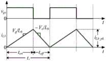
图2是CRM Buck-Boost PFC变换器的电感电流波形图。Figure 2 is the inductor current waveform diagram of the CRM Buck-Boost PFC converter.
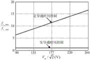
图3是变导通时间控制时开关频率随输入电压的变化曲线图。FIG. 3 is a graph showing the change of switching frequency with input voltage during variable on-time control.
图4是两种控制方式下PF值与Vm的关系曲线图。Figure 4 is a graph showing the relationship between PF value and Vm under two control modes.
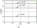
图5是3、5、7次谐波与输入电压的关系曲线图。Figure 5 is a graph showing the relationship between the 3rd, 5th and 7th harmonics and the input voltage.
图6是不同输入电压下的临界电感值变化曲线图。FIG. 6 is a graph showing the change of the critical inductance value under different input voltages.
图7是fs在半个工频周期内的变化曲线图,其中(a)为定导通时间控制的变化曲线图,(b)为变导通时间控制的变化曲线图。FIG. 7 is a change curve diagram of fs in half a power frequency cycle, wherein (a) is a change curve diagram of constant on-time control, and (b) is a change curve diagram of variable on-time control.
图8是两种控制方式下最大与最小开关频率之比随输入电压的变化曲线图。Figure 8 is a graph showing the variation of the ratio of the maximum and minimum switching frequencies with the input voltage under the two control modes.
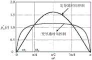
图9是两种控制方式下瞬时输入功率标幺值在半个工频周期内的变化曲线图。FIG. 9 is a graph showing the variation of the per-unit value of instantaneous input power in half a power frequency cycle under two control modes.
图10是两种控制方式下输出纹波的变化曲线图。Fig. 10 is the change curve diagram of the output ripple under two control modes.
图11是本发明恒定开关频率的CRM Buck-Boost PFC变换器的电路结构示意图。11 is a schematic diagram of the circuit structure of the CRM Buck-Boost PFC converter with constant switching frequency of the present invention.
具体实施方式Detailed ways
1CRM Buck-Boost PFC变换器的工作原理1CRM Buck-Boost PFC Converter Working Principle
图1是Buck-Boost PFC变换器主电路。Fig. 1 is the main circuit of Buck-Boost PFC converter.
作如下假设:1.所有器件均为理想元件;2.输出电压纹波与其直流量相比很小;3.开关频率远高于输入电压频率。The following assumptions are made: 1. All devices are ideal components; 2. The output voltage ripple is small compared to its DC value; 3. The switching frequency is much higher than the input voltage frequency.
不失一般性,定义输入交流电压的表达式为:Without loss of generality, the expression defining the input AC voltage is:
vin=Vmsinωt (1)vin =Vm sinωt (1)
其中Vm和ω分别为输入交流电压的幅值和角频率。where Vm and ω are the amplitude and angular frequency of the input AC voltage, respectively.
那么输入整流后的电压为:Then the input voltage after rectification is:
vg=Vm|sinωt| (2)vg =Vm |sinωt| (2)
图2为一个开关周期内变换器的电感电流波形。当开关管Qb导通时,二极管Db截止,电感Lb储能,电感两端的电压为vg,其电流iL由零开始以vg/Lb的斜率线性上升,那么iLb的峰值为:Figure 2 shows the inductor current waveform of the converter in one switching cycle. When the switch tube Qb is turned on, the diode Db is turned off, the inductor Lb stores energy, the voltage across the inductor is vg , and the current iL starts from zero and rises linearly with the slope of vg /Lb , then the value of iLb The peaks are:
其中ton为Qb的导通时间。where ton is the on-time of Qb .
当开关管Qb关断,二极管Db导通时,通过电感Lb电流iLb续流,此时Lb两端的电压为-Vo,iLb以Vo/Lb的斜率从电感电流峰值iLb_pk下降,其下降到零的时间toff为:When the switch tube Qb is turned off and the diode Db is turned on, the current iLb continues to flow through the inductor Lb . At this time, the voltage acrossLb is-Vo .Lb_pkdrops , and the time toff that it drops to zero is:

由于Buck-Boost变换器工作在CRM模式,因此当二极管Db的电流下降到零时,开关管Qb开通,开始新的开关周期。Since the Buck-Boost converter works in the CRM mode, when the current of the diode Db drops to zero, the switch tube Qb is turned on, and a new switching cycle begins.
由式(4)可以看出,如果在一个工频周期内,开关管Qb导通时间ton是固定的,开关管Qb关断时间toff是随输入电压瞬时值变化的,即一个工频周期中开关频率不断变化。It can be seen from equation (4) that if in a power frequency cycle, the on-time ton of the switch Qb is fixed, and the off time toff of the switch Qb varies with the instantaneous value of the input voltage, that is, a The switching frequency is constantly changing during the power frequency cycle.
由式(4)可得占空比为:From equation (4), the duty cycle can be obtained as:
d(t)=ton/(ton+toff)=Vo/(Vo+Vm|sinωt) (5)d(t)=ton /(ton+ tff )=Vo/(Vo+ Vm |sinωt) (5)
由式(3)和(5),一个开关周期内,电感电流的平均值iL_av为:From equations (3) and (5), the average value of the inductor current iL _av in one switching cycle is:

那么,输入电流iin为:Then, the input current iin is:

由式(1)和式(7),可以求出在半个工频周期内输入功率的平均值Pin:From equations (1) and (7), the average value Pin of the input power in half the power frequency cycle can be obtained:

设定变换器效率为100%,那么输入功率等于输出功率,即Pin=Po。由式(8)可得开关管Qb导通时间ton:Assuming that the converter efficiency is 100%, then the input power is equal to the output power, that is, Pin =Po . From the formula (8), the conduction time ton of the switch tube Qb can be obtained:

由式(7)、式(8)和式(9)可以求得PF值的表达式为:From formula (7), formula (8) and formula (9), the expression of PF value can be obtained as:

由式(4)和式(9)可得:From formula (4) and formula (9), we can get:

通过式(11)可知,工频周期中开关频率最大和最小的时刻分别为输入电压过零和峰值处,即ωt=0和ωt=π/2时,即:According to formula (11), the maximum and minimum switching frequency in the power frequency cycle are the zero-crossing and peak values of the input voltage, respectively, that is, when ωt=0 and ωt=π/2, that is:


二者之比为:The ratio of the two is:

由式(13)可知,如果限定最低开关频率,则最大电感值的表达式为:It can be seen from equation (13) that if the minimum switching frequency is limited, the expression of the maximum inductance value is:

2恒定开关频率的控制策略2 Control strategy for constant switching frequency
观察传统定导通时间控制CRM Buck-Boost PFC变换器的开关频率表达式(11),如果取导通时间为:Observe the switching frequency expression (11) of the traditional constant on-time control CRM Buck-Boost PFC converter, if the on-time is taken as:

式中KT为一个常数,则开关频率fs可表示为:Where KT is a constant, the switching frequency fs can be expressed as:
由式(17)可知,如果使CRM Buck-Boost PFC变换器的开关管Qb的导通时间ton在一个工频周期内按照式(16)变化,则可以使开关频率在工频周期内为恒定值。It can be seen from equation (17) that if the on-time ton of the switching tube Qb of the CRM Buck-Boost PFC converter is changed according to equation (16) within a power frequency period, the switching frequency can be made within the power frequency period. is a constant value.
把式(16)代入式(8),可以求出在半个工频周期内输入功率的平均值Pin:Substituting Equation (16) into Equation (8), the average value Pin of the input power in half the power frequency cycle can be obtained:

由式(18)可得常数KT为:From equation (18), the constant KT can be obtained as:
把式(19)代入式(16)中,可得:Substituting equation (19) into equation (16), we can get:

结合式(17)和式(19)可知:Combining equations (17) and (19), it can be known that:

由式(21)可知,当输入电压Vm一定时,半个工频周期内fs为恒定值。结合3.1节设计指标,取变导通时间控制下的电感值Lb=86uH,根据式(21)作出开关频率fs随输入电压Vm的变化规律曲线,如图3所示。It can be known from formula (21) that when the input voltage Vm is constant, fs is a constant value in half the power frequency cycle. Combined with the design index in Section 3.1, take the inductance value Lb = 86uH under the control of the on-time, and make the change rule curve of the switching frequency fs with the input voltage Vm according to formula (21), as shown in Figure 3.
3性能对比3 Performance comparison
3.1PF变化3.1PF changes
设计参数如下:The design parameters are as follows:
输入电压有效值Vin_rms=90~264VAC;输出功率Po=60W;输出电压Vo=24V;最低开关频率fs_min=30kHz。The effective value of the input voltage Vin_rms =90~264VAC; the output power Po =60W; the output voltage Vo =24V; the minimum switching frequency fs_min =30kHz.
由式(7)、式(16)和式(18)可得PF值的表达式为:The expression for the PF value that can be obtained from equations (7), (16) and (18) is:

根据变换器的设计参数,由式(10)和式(22)可作出两种控制方式下PF值与Vm的关系曲线,如图4所示。从图中可以看出,在90V~264V AC输入电压范围内,采用变导通时间控制后,PF值有所降低,输入电压越高,降低幅度越大,当输入电压为264VAC时,PF值从0.943降到0.604。According to the design parameters of the converter, the relationship curve between the PF value and Vm under the two control modes can be made by formula (10) and formula (22), as shown in Figure 4. It can be seen from the figure that within the input voltage range of 90V ~ 264V AC, after the variable on-time control is used, the PF value is reduced. The higher the input voltage, the greater the reduction range. When the input voltage is 264VAC, the PF value From 0.943 to 0.604.
将式(16)代入式(7)可得输入电流:Substitute equation (16) into equation (7) to obtain the input current:

为了分析输入电流的谐波,可以对其进行傅里叶分解。输入电流的傅立叶分解形式为:In order to analyze the harmonics of the input current, it can be Fourier decomposition. The Fourier decomposition form of the input current is:

其中in

式中Tline是输入电压周期。Where Tline is the input voltage period.
将式(23)代入式(25),经计算可得变导通时间控制下输入电流所含的各次谐波。其中,余弦成分和偶次正弦成分均为0,即:Substitute Equation (23) into Equation (25), and after calculation, the harmonics contained in the input current under the control of variable on-time can be obtained. Among them, the cosine component and the even sine component are both 0, namely:
由式(23)、式(25)和式(26)可得:From formula (23), formula (25) and formula (26), we can get:
其中
根据IEC61000-3-2,Class D标准要求,输入电流3、5、7次谐波与输入功率之比应满足式(28)According to the requirements of IEC61000-3-2, Class D standard, the ratio of the 3rd, 5th, and 7th harmonics of the input current to the input power should satisfy the formula (28)

即which is


根据变换器的设计参数,Vm从

3.2临界电感值及开关频率的变化3.2 Changes in critical inductance value and switching frequency
由式(21)可知,如果限定最低开关频率为fs_min,则最大电感值的表达式为:It can be known from equation (21) that if the minimum switching frequency is limited to fs_min , the expression of the maximum inductance value is:

根据变换器的设计参数,由式(15)和式(30)可得到图6。从图中可以看出,定导通时间控制和变导通时间控制下的临界电感值分别为Lb1=48uH和Lb2=58uH。According to the design parameters of the converter, Figure 6 can be obtained from equation (15) and equation (30). It can be seen from the figure that the critical inductance values under constant on-time control and variable on-time control are Lb1 =48uH and Lb2 =58uH, respectively.
将Lb1=48uH代入式(11),将Lb2=58uH代入式(21),由变换器的参数,可作出两种控制方式下fs在半个工频周期内的变化曲线,如图7(a)~(b)所示。Substitute Lb1 =48uH into equation (11), and substitute Lb2 =58uH into equation (21), from the parameters of the converter, the change curve of fs in half the power frequency cycle under the two control modes can be drawn, as shown in the figure 7(a) to (b).
由式(21)可知,工频周期内开关频率最大值等于最小值,即开关频率为恒定值,因此可知变导通时间控制时It can be seen from equation (21) that the maximum value of the switching frequency in the power frequency cycle is equal to the minimum value, that is, the switching frequency is a constant value, so it can be seen that when the on-time control is variable

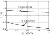
根据式(14)和式(31)作出图8,从图中可以看出,采用变导通时间控制后,开关频率最大值与最小值之比降低为1,输入电压越高,降低幅度越大。Figure 8 is made according to formula (14) and formula (31). It can be seen from the figure that after the variable on-time control is adopted, the ratio of the maximum value to the minimum value of the switching frequency is reduced to 1. The higher the input voltage, the greater the reduction range. big.
3.3输出电压纹波的减小3.3 Reduction of output voltage ripple
采用定导通时间控制时,由式(1)、式(7)和式(9)可得变换器的瞬时输入功率标幺值(基准值为输出功率)为:When the constant on-time control is adopted, the instantaneous input power per unit value of the converter (the reference value is the output power) can be obtained from equations (1), (7) and (9) as:

采用变导通时间控制时,由式(1)、式(18)和式(23)可得变换器的瞬时输入功率标幺值(基准值为输出功率)为:When the variable on-time control is used, the instantaneous input power per unit value of the converter (the reference value is the output power) can be obtained from equations (1), (18) and (23) as:

由式(32)和式(33)可以作出两种控制方式下的瞬时输入功率标幺值在半个工频周期内的变化曲线,如图9所示。From the formula (32) and the formula (33), the change curve of the per-unit value of the instantaneous input power in half the power frequency cycle under the two control modes can be obtained, as shown in Figure 9.
当


根据电容储能的计算公式,

其中ΔVo1和ΔVo2分别是定导通时间和变导通时间控制下的输出电压纹波值。Among them, ΔVo1 and ΔVo2 are the output voltage ripple values under the control of constant on-time and variable on-time, respectively.
由式(36)和式(37)可得输出电压纹波为:From equation (36) and equation (37), the output voltage ripple can be obtained as:

由式(38)可作出图10,从图中可以看出,采用变导通时间控制后,当输入电压为90VAC时,输出电压纹波减小为原来的58.3%,当输入电压为264VAC时,输出电压纹波减小为原来的38.5%。Figure 10 can be drawn from equation (38). It can be seen from the figure that after the variable on-time control is adopted, when the input voltage is 90VAC, the output voltage ripple is reduced to 58.3% of the original, and when the input voltage is 264VAC , the output voltage ripple is reduced to 38.5% of the original.
4本发明恒定开关频率的CRM Buck-Boost PFC变换器4 CRM Buck-Boost PFC converter with constant switching frequency of the present invention
结合图11,第一电容C1和第一二极管D1组成辅助绕组整流电路,电感Lb的辅助绕组Lz的异名端经该辅助绕组整流电路后得到vA=Vo,vA经第一电阻R1和第二电阻R2分压得到vB=R2vA/(R1+R2)。输入电压vg经第三电阻R3和第四电阻R4分压得到vC=R4Vm|sinωt|/(R3+R4)。vB与vC接入加法电路,其中R7=R8=R10=R11=2R9,则输出vD==R2vA/(R1+R2)+R4Vm|sinωt|/(R3+R4)。通过设定R1、R2、R3和R4的值,使其满足关系R2/(R1+R2)=R4/(R3+R4),则vB=VoR4/(R3+R4),vD=[(Vo/Vm|sinωt|)R4]/(R3+R4),输出电压Vo经整流电路和反馈误差调节电路得到误差信号vEA,vB、vD与vEA接入乘法器,其输出vp=vEA/(1+Vm|sinωt|/Vo),将vp与采样电阻Rd比较后可得到如式(20)所示变化规律的导通时间。其中vA、vB、vC、vD、vp分别为辅助绕组整流电路2、第一分压跟随电路4、第二分压跟随电路5、加法电路6、乘法器7的电压输出值。Referring to Fig. 11, the first capacitorC1 and thefirst diode D1 form an auxiliary winding rectifier circuit, and the synonymous end of the auxiliary winding Lz of the inductorLb obtainsvA =Vo , v after passing through the auxiliary winding rectifier circuitA is divided by the first resistor R1 and the second resistor R2 to obtain vB =R2 vA /(R1 +R2 ). The input voltage vg is divided by the third resistor R3 and the fourth resistor R4 to obtain vC =R4 Vm |sinωt|/(R3 +R4 ). vB and vC are connected to the adding circuit, wherein R7 =R8 =R10 =R11 =2R9 , then the output vD ==R2 vA /(R1 +R2 )+R4 Vm | sinωt|/(R3 +R4 ). By setting the values of R1 , R2 , R3 and R4 to satisfy the relation R2 /(R1 +R2 )=R4 /(R3 +R4 ), then vB =Vo R4 /(R3 +R4 ), vD =[(Vo /Vm |sinωt|)R4 ]/(R3 +R4 ), the output voltage Vo obtains the error through the rectifier circuit and the feedback error adjustment circuit The signals vEA , vB , vD and vEA are connected to the multiplier, and the output vp =vEA /(1+Vm |sinωt|/Vo ) can be obtained by comparing vp with the sampling resistor Rd As shown in formula (20), the on-time of the variation law is shown. Wherein vA , vB , vC , vD , vp are the voltage output values of the auxiliary winding
具体电路如下:The specific circuit is as follows:
本发明的恒定开关频率的CRM Buck-Boost PFC变换器,包括主功率电路1和控制电路;The CRM Buck-Boost PFC converter with constant switching frequency of the present invention includes a main power circuit 1 and a control circuit;
所述主功率电路1包括输入电压源vin、EMI滤波器、二极管整流电路RB、电感Lb、开关管Qb、采样电阻Rd、二极管Db、滤波电容Co和负载RLd;其中输入电压源vin与EMI滤波器的输入端口连接,EMI滤波器的输出端口与二极管整流电路RB的输入端口连接,二极管整流电路RB的输出负极为参考电位零点,二极管整流电路RB的输出正极与开关管Qb的源极连接,电感Lb的绕组Lb的同名端接入开关管Qb的漏极,采样电阻Rd与驱动信号生成电路连接,电感Lb的辅助绕组Lz的异名端与参考电位零点连接,电感Lb的绕组Lb的同名端与二极管Db的阳极连接,二极管Db的阴极分别与滤波电容Co的一端和负载RLd的一端连接,滤波电容Co的另一端和负载RLd的另一端均连接参考电位零点,负载RLd两端的电压为输出电压Vo;The main power circuit 1 includes an input voltage source vin , an EMI filter, a diode rectifier circuit RB, an inductor Lb , a switch tube Qb , a sampling resistor Rd , a diode Db , a filter capacitor Co and a load RLd ; wherein The input voltage source vin is connected to the input port of the EMI filter, the output port of the EMI filter is connected to the input port of the diode rectifier circuit RB, the output cathode of the diode rectifier circuit RB is the reference potential zero point, and the output anode of the diode rectifier circuit RB is connected to the The source of the switch tube Qb is connected, the same-named end of the winding Lb of the inductor Lb is connected to the drain of the switch tube Qb , the sampling resistor Rd is connected to the driving signal generating circuit, and the difference of the auxiliary winding Lz of the inductor Lb is different. The name terminal is connected to the reference potential zero point, the same name terminal of the winding Lb of the inductor Lb is connected to the anode of the diode Db , and the cathode of the diode Db is connected to one end of the filter capacitor Co and one end of the load RLd respectively, and the filter capacitor C The other end ofo and the other end of the load RLd are both connected to the reference potential zero point, and the voltage across the load RLd is the output voltage Vo ;
所述的控制电路采用导通时间变化规律为KT/(1+Vm|sinωt|/Vo)的输出信号驱动开关管Qb,包括辅助绕组整流电路2、CRM驱动信号生成电路3、第一分压跟随电路4、第二分压跟随电路5、加法电路6、乘法器7和原边反馈误差调节电路8,其中辅助绕组整流电路2的输入端与变压器T1的绕组Nz的同名端连接,辅助绕组整流电路2的输出端A分别与第一分压跟随电路4的一个输入端和原边反馈误差调节电路8的一个输入端连接,CRM驱动信号生成电路3的输出端与开关管Qb的门极连接,第一分压跟随电路4的输出端B分别与加法电路6的一个输入端和乘法器7的第一输入端vx连接,第二分压跟随电路5的输入端与输入电压采样点Vg即二极管整流电路RB的输出正极连接,第二分压跟随电路5的输出端C与加法电路6的另一个输入端连接,加法电路6的输出端D与乘法器7的第三输入端vz连接,乘法器7的输出端vp接入CRM驱动信号生成电路3的输入端,原边反馈误差调节电路8的输出端与乘法器7的第二输入端vy连接。The control circuit uses an output signal whose on-time variation law is KT /(1+Vm |sinωt|/Vo ) to drive the switch tube Qb , and includes an auxiliary winding
所述的控制电路采用导通时间变化规律为KT/(1+Vm|sinωt|/Vo)的输出信号驱动开关管Qb,其中:The control circuit uses an output signal whose on-time variation law is KT /(1+Vm |sinωt|/Vo ) to drive the switch Qb , wherein:
Vm和ω分别为输入交流电压的幅值和角频率,Po为输出功率,Lb为电感。Vm and ω are the amplitude and angular frequency of the input AC voltage, respectively, Po is the output power, and Lb is the inductance.
所述的辅助绕组整流电路2包括第一二极管D1、第一电容C1;第一二极管D1的正极与变压器T1的绕组Nz的同名端连接,第一电容C1的一端与第一二极管D1的负极连接、另一端接参考电位零点,第一电容C1与第一二极管D1的公共端即辅助绕组整流电路2的输出端A接入第一分压跟随电路4。The auxiliary winding
所述的CRM驱动信号生成电路3包括过零检测、RS触发器、驱动、锯齿波发生器、第一运算放大器A1;过零检测的输入端与变压器T1的绕组Nz的同名端连接,过零检测的输出端与RS触发器的S端连接,RS触发器的R端与第一运算放大器A1的输出端连接,RS触发器的Q端与驱动的输入端和锯齿波发生器的输入端连接,锯齿波发生器的输出端与第一运算放大器A1的正向输入端连接,第一运算放大器A1的反向输入端即CRM驱动信号生成电路3的输入端与乘法器7的输出端vp连接。The CRM drive signal generating circuit 3 includes zero-crossing detection, RS trigger, driving, sawtooth wave generator, and a first operational amplifier A1 ; the input end of the zero-crossing detection is connected to the same-named end of the winding Nz of the transformer T1 . , the output terminal of zero-crossing detection is connected with the S terminal of the RS flip-flop, the R terminal of the RS flip-flop is connected with the output terminal of thefirst operational amplifier A1, the Q terminal of the RS flip-flop is connected with the input terminal of the drive and the sawtooth wave generator The input end of the sawtooth wave generator is connected to the forward input end of thefirst operational amplifier A1, the reverse input end of thefirst operational amplifier A1 is the input end of the CRM drive signal generating circuit 3 and the multiplier The output of 7 is connected tovp .
所述第一分压跟随电路4包括第一电阻R1、第二电阻R2、第二运算放大器A2;其中第一电阻R1的一端与辅助绕组整流电路2的输出端A连接,第一电阻R1的另一端与第二电阻R2一端连接且公共端接入第二运算放大器A2的正向输入端,第二电阻R2的另一端与参考电位零点连接,第二运算放大器A2的反向输入端与输出端B直接连接,构成同相电压跟随器。The first voltage
所述第二分压跟随电路5包括第三电阻R3、第四电阻R4、第三运算放大器A3;其中第三电阻R3的一端与输入电压采样点Vg即二极管整流电路RB的输出正极连接,第三电阻R3的另一端与第四电阻R4一端连接且公共端接入第二运算放大器A3的正向输入端,第四电阻R4的另一端与参考电位零点连接,第三运算放大器A3的反向输入端与输出端C直接连接,构成同相电压跟随器。The second voltage
所述加法电路6包括第七电阻R7、第八电阻R8、第九电阻R9、第十电阻R10、第十一电阻R11、第四运算放大器A4;其中第七电阻R7一端与第二分压跟随电路5的输出端C连接、另一端接入第四运算放大器A4的正向输入端,第八电阻R8的一端接入第一分压跟随电路4的输出端B连接、另一端接入第四运算放大器A4的正向输入端,第九电阻R9一端接入第四运算放大器A4的反向输入端、另一端接入参考电位零点,第十电阻R10一端接入第四运算放大器A4的正向输入端、另一端接入参考电位零点,第十一电阻R11接入第四运算放大器A4的反向输入端和输出端D之间。The adding
所述原边反馈误差调节电路8包括第五电阻R5、第六电阻R6、第十二电阻R12、第二电容C2、第五运算放大器A5;其中第五电阻R5的一端与辅助绕组整流电路2的输出端A连接、另一端接入第五运算放大器A5的反向输入端,第六电阻R6的一端接入第五运算放大器A5的反向输入端、另一端接入参考电位零点,第十二电阻R12与第二电容C2串联后接入第五运算放大器A5的反向输入端和输出端之间,第五运算放大器A5的正向输入端与输入电压参考点Vref连接。The primary-side feedback error adjustment circuit 8 includes a fifth resistor R5 , a sixth resistor R6 , a twelfth resistor R12 , a second capacitor C2 , and a fifth operational amplifier A5 ; one end of the fifth resistor R5 It is connected to the output end A of the auxiliary winding
综上所述,本发明的恒定开关频率的CRM Buck-Boost PFC变换器,采用变导通时间控制实现了工频周期内开关频率为恒定值,即最大值与最小值之比为1,并减小了输出电压纹波。To sum up, the CRM Buck-Boost PFC converter with constant switching frequency of the present invention adopts variable on-time control to realize that the switching frequency in the power frequency cycle is a constant value, that is, the ratio of the maximum value to the minimum value is 1, and the Reduced output voltage ripple.
Claims (8)
Priority Applications (1)
| Application Number | Priority Date | Filing Date | Title |
|---|---|---|---|
| CN201810889244.8ACN110829827A (en) | 2018-08-07 | 2018-08-07 | CRM boost-buck PFC converter with constant switching frequency |
Applications Claiming Priority (1)
| Application Number | Priority Date | Filing Date | Title |
|---|---|---|---|
| CN201810889244.8ACN110829827A (en) | 2018-08-07 | 2018-08-07 | CRM boost-buck PFC converter with constant switching frequency |
Publications (1)
| Publication Number | Publication Date |
|---|---|
| CN110829827Atrue CN110829827A (en) | 2020-02-21 |
Family
ID=69533706
Family Applications (1)
| Application Number | Title | Priority Date | Filing Date |
|---|---|---|---|
| CN201810889244.8APendingCN110829827A (en) | 2018-08-07 | 2018-08-07 | CRM boost-buck PFC converter with constant switching frequency |
Country Status (1)
| Country | Link |
|---|---|
| CN (1) | CN110829827A (en) |
Cited By (3)
| Publication number | Priority date | Publication date | Assignee | Title |
|---|---|---|---|---|
| CN111541387A (en)* | 2020-04-30 | 2020-08-14 | 南京理工大学 | A CRM Boost Converter Based on Variable Inductance Frequency Optimal Control |
| CN112366940A (en)* | 2021-01-18 | 2021-02-12 | 四川大学 | Voltage and current quasi-fixed frequency control device and method |
| CN113922664A (en)* | 2021-09-30 | 2022-01-11 | 南京理工大学 | Power conversion device with low-frequency large-pulse current output and no-pulse current input |
Citations (1)
| Publication number | Priority date | Publication date | Assignee | Title |
|---|---|---|---|---|
| CN104734487A (en)* | 2015-03-13 | 2015-06-24 | 南京理工大学 | CRM Flyback PFC converter achieving constant switching frequency |
- 2018
- 2018-08-07CNCN201810889244.8Apatent/CN110829827A/enactivePending
Patent Citations (1)
| Publication number | Priority date | Publication date | Assignee | Title |
|---|---|---|---|---|
| CN104734487A (en)* | 2015-03-13 | 2015-06-24 | 南京理工大学 | CRM Flyback PFC converter achieving constant switching frequency |
Non-Patent Citations (1)
| Title |
|---|
| XUESHAN LIU等: "Single-Inductor Dual-Output Buck–Boost Power Factor Correction Converter", 《IEEE》* |
Cited By (6)
| Publication number | Priority date | Publication date | Assignee | Title |
|---|---|---|---|---|
| CN111541387A (en)* | 2020-04-30 | 2020-08-14 | 南京理工大学 | A CRM Boost Converter Based on Variable Inductance Frequency Optimal Control |
| CN111541387B (en)* | 2020-04-30 | 2022-07-05 | 南京理工大学 | A CRM Boost Converter Based on Variable Inductance Frequency Optimal Control |
| CN112366940A (en)* | 2021-01-18 | 2021-02-12 | 四川大学 | Voltage and current quasi-fixed frequency control device and method |
| CN112366940B (en)* | 2021-01-18 | 2021-04-23 | 四川大学 | Voltage and current quasi-fixed frequency control device and method |
| CN113922664A (en)* | 2021-09-30 | 2022-01-11 | 南京理工大学 | Power conversion device with low-frequency large-pulse current output and no-pulse current input |
| CN113922664B (en)* | 2021-09-30 | 2024-04-16 | 南京理工大学 | Low-frequency large-ripple current output power conversion device without ripple current input |
Similar Documents
| Publication | Publication Date | Title |
|---|---|---|
| CN104242692B (en) | CRM Boost PFC Converter with Optimal Frequency Variation Range | |
| CN101764528B (en) | High power factor DCM Boost PFC converter | |
| CN104967323B (en) | Low Output Voltage Ripple Discontinuous Mode Flyback Power Factor Correction Converter | |
| CN105226931B (en) | Improve the control device of DCM Buck pfc converter PF values | |
| CN103813591B (en) | The CRM Flyback LED driver of low output current peak-to-average force ratio | |
| CN103414334B (en) | PF is the long-life DCM Boost pfc converter of 1 | |
| CN111541386B (en) | High PF (positive-frequency) fixed switching frequency boost converter of parallel active filter | |
| CN111865117B (en) | DCM buck-boost PFC converter controlled by segmented fixed duty ratio | |
| CN104734487A (en) | CRM Flyback PFC converter achieving constant switching frequency | |
| CN106533152A (en) | Device and method for improving PF of Boost three-level converter | |
| CN116191862A (en) | Bridgeless buck PFC converter based on buck and flyback conversion unit | |
| CN109149963A (en) | The DCM of switch periods optimal utilization rate control is depressured pfc converter | |
| CN104702131A (en) | CRM Buck PFC convertor with optimal frequency variation range | |
| CN110829827A (en) | CRM boost-buck PFC converter with constant switching frequency | |
| CN104702108A (en) | Critical continuous boost converter employing constant-frequency control | |
| CN116722734A (en) | Bridgeless buck PFC converter based on buck-boost conversion unit | |
| CN109309447B (en) | Constant switching frequency controlled CRM buck PFC converter | |
| CN119010560B (en) | A four-tube Buck-Boost PFC converter control method and control circuit | |
| CN110518818A (en) | CRM decompression-flyback pfc converter of fixed-frequency control | |
| CN112421943B (en) | A power factor correction control circuit and driving power supply | |
| CN110289755B (en) | High Power Factor DCM Buck-Flyback PFC Converter | |
| CN116961400B (en) | High-efficiency bridgeless buck PFC converter without input diode | |
| CN110932576B (en) | DCM Buck-Boost PFC Converter with Constant Switching Cycle Utilization | |
| CN110829822B (en) | CRM Boost PFC converter for optimizing frequency variation range | |
| CN111865065B (en) | High power factor DCM buck-boost PFC converter |
Legal Events
| Date | Code | Title | Description |
|---|---|---|---|
| PB01 | Publication | ||
| PB01 | Publication | ||
| SE01 | Entry into force of request for substantive examination | ||
| SE01 | Entry into force of request for substantive examination | ||
| RJ01 | Rejection of invention patent application after publication | Application publication date:20200221 | |
| RJ01 | Rejection of invention patent application after publication |