CN110829552A - Wireless charging system, charging cable, electronic device and wireless charging method thereof - Google Patents
Wireless charging system, charging cable, electronic device and wireless charging method thereofDownload PDFInfo
- Publication number
- CN110829552A CN110829552ACN201911038156.8ACN201911038156ACN110829552ACN 110829552 ACN110829552 ACN 110829552ACN 201911038156 ACN201911038156 ACN 201911038156ACN 110829552 ACN110829552 ACN 110829552A
- Authority
- CN
- China
- Prior art keywords
- charging
- receiving
- electronic device
- transmitting
- magnetic
- Prior art date
- Legal status (The legal status is an assumption and is not a legal conclusion. Google has not performed a legal analysis and makes no representation as to the accuracy of the status listed.)
- Pending
Links
Images


Classifications
- H—ELECTRICITY
- H02—GENERATION; CONVERSION OR DISTRIBUTION OF ELECTRIC POWER
- H02J—CIRCUIT ARRANGEMENTS OR SYSTEMS FOR SUPPLYING OR DISTRIBUTING ELECTRIC POWER; SYSTEMS FOR STORING ELECTRIC ENERGY
- H02J50/00—Circuit arrangements or systems for wireless supply or distribution of electric power
- H02J50/10—Circuit arrangements or systems for wireless supply or distribution of electric power using inductive coupling
- H02J50/12—Circuit arrangements or systems for wireless supply or distribution of electric power using inductive coupling of the resonant type
- H—ELECTRICITY
- H02—GENERATION; CONVERSION OR DISTRIBUTION OF ELECTRIC POWER
- H02J—CIRCUIT ARRANGEMENTS OR SYSTEMS FOR SUPPLYING OR DISTRIBUTING ELECTRIC POWER; SYSTEMS FOR STORING ELECTRIC ENERGY
- H02J50/00—Circuit arrangements or systems for wireless supply or distribution of electric power
- H02J50/40—Circuit arrangements or systems for wireless supply or distribution of electric power using two or more transmitting or receiving devices
- H—ELECTRICITY
- H02—GENERATION; CONVERSION OR DISTRIBUTION OF ELECTRIC POWER
- H02J—CIRCUIT ARRANGEMENTS OR SYSTEMS FOR SUPPLYING OR DISTRIBUTING ELECTRIC POWER; SYSTEMS FOR STORING ELECTRIC ENERGY
- H02J50/00—Circuit arrangements or systems for wireless supply or distribution of electric power
- H02J50/70—Circuit arrangements or systems for wireless supply or distribution of electric power involving the reduction of electric, magnetic or electromagnetic leakage fields
- H—ELECTRICITY
- H02—GENERATION; CONVERSION OR DISTRIBUTION OF ELECTRIC POWER
- H02J—CIRCUIT ARRANGEMENTS OR SYSTEMS FOR SUPPLYING OR DISTRIBUTING ELECTRIC POWER; SYSTEMS FOR STORING ELECTRIC ENERGY
- H02J50/00—Circuit arrangements or systems for wireless supply or distribution of electric power
- H02J50/80—Circuit arrangements or systems for wireless supply or distribution of electric power involving the exchange of data, concerning supply or distribution of electric power, between transmitting devices and receiving devices
- H—ELECTRICITY
- H02—GENERATION; CONVERSION OR DISTRIBUTION OF ELECTRIC POWER
- H02J—CIRCUIT ARRANGEMENTS OR SYSTEMS FOR SUPPLYING OR DISTRIBUTING ELECTRIC POWER; SYSTEMS FOR STORING ELECTRIC ENERGY
- H02J50/00—Circuit arrangements or systems for wireless supply or distribution of electric power
- H02J50/90—Circuit arrangements or systems for wireless supply or distribution of electric power involving detection or optimisation of position, e.g. alignment
Landscapes
- Engineering & Computer Science (AREA)
- Computer Networks & Wireless Communication (AREA)
- Power Engineering (AREA)
- Physics & Mathematics (AREA)
- Electromagnetism (AREA)
- Charge And Discharge Circuits For Batteries Or The Like (AREA)
Abstract
Translated fromChinese
Description
Translated fromChinese技术领域technical field
本申请实施例涉及无线充电技术领域,尤其涉及一种无线充电系统、电子设备、充电线缆以及一种无线充电方法。The embodiments of the present application relate to the technical field of wireless charging, and in particular, to a wireless charging system, an electronic device, a charging cable, and a wireless charging method.
背景技术Background technique
目前,充电器可通过无线充电方式对电子设备(例如手机等)进行充电。电子设备用于实现无线充电的接收线圈采用扁平螺旋线构造,充电器用于实现无线充电的发射线圈也采用扁平螺旋线构造。由于接收线圈的外径尺寸较大,需要占用较大的面积,因此安装在电子设备的具有较大平面的一侧,例如电子设备的后盖。充电器也由于发射线圈的外径尺寸较大,而采用面积较大的扁平式结构。电子设备充电时,需要放置在充电器上方并且电子设备的后盖接触充电器,使得接收线圈正对发射线圈。如此一来,用户无法在电子设备进行无线充电时握持和使用电子设备,导致无线充电的使用体验较差。Currently, chargers can charge electronic devices (such as mobile phones, etc.) through wireless charging. The receiving coil used by the electronic device to realize wireless charging adopts a flat spiral structure, and the transmitting coil used by the charger to realize wireless charging also adopts a flat spiral structure. Since the outer diameter of the receiving coil is large, it needs to occupy a large area, so it is installed on the side of the electronic device with a large plane, such as the back cover of the electronic device. The charger also adopts a flat structure with a larger area due to the larger outer diameter of the transmitting coil. When charging the electronic device, it needs to be placed above the charger and the back cover of the electronic device is in contact with the charger, so that the receiving coil is facing the transmitting coil. As a result, the user cannot hold and use the electronic device while the electronic device is being wirelessly charged, resulting in a poor experience in using wireless charging.
发明内容SUMMARY OF THE INVENTION
本申请的目的在于提供了一种无线充电系统、电子设备、充电线缆以及无线充电方法。无线充电系统中的电子设备通过充电线缆进行无线充电时,用户能够握持和使用电子设备,从而提高了无线充电场景下的用户使用体验。The purpose of the present application is to provide a wireless charging system, an electronic device, a charging cable and a wireless charging method. When the electronic device in the wireless charging system is wirelessly charged through the charging cable, the user can hold and use the electronic device, thereby improving the user experience in the wireless charging scenario.
第一方面,本申请实施例提供一种无线充电系统。无线充电系统包括电子设备和充电线缆。充电线缆用于对电子设备进行充电。In a first aspect, an embodiment of the present application provides a wireless charging system. A wireless charging system includes an electronic device and a charging cable. Charging cables are used to charge electronic devices.
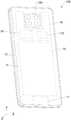
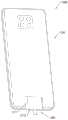
电子设备包括后盖、边框、接收磁棒、接收线圈以及电池。边框环绕地连接于后盖的周缘。接收磁棒位于边框内侧。接收磁棒包括第一接收耦合面和与第一接收耦合面相交的第二接收耦合面,第二接收耦合面的面积大于第一接收耦合面的面积,第一接收耦合面面向边框设置,第二接收耦合面面向后盖设置。接收线圈缠绕于接收磁棒的中部。电池位于边框内侧且电连接接收线圈。The electronic device includes a back cover, a frame, a receiving magnetic rod, a receiving coil and a battery. The frame is circumferentially connected to the periphery of the back cover. The receiving magnet is located inside the frame. The receiving magnetic bar includes a first receiving coupling surface and a second receiving coupling surface intersecting with the first receiving coupling surface, the area of the second receiving coupling surface is larger than that of the first receiving coupling surface, the first receiving coupling surface is arranged facing the frame, and the second receiving coupling surface is arranged toward the frame. Two receiving coupling surfaces are arranged facing the back cover. The receiving coil is wound around the middle of the receiving magnet bar. The battery is located inside the frame and is electrically connected to the receiving coil.
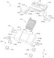
充电线缆包括充电头外壳、发射磁棒以及发射线圈。充电头外壳包括外壳端面和连接于外壳端面周缘的外壳侧面。发射磁棒位于充电头外壳的内部。发射磁棒包括第一发射耦合面和与第一发射耦合面相交的第二发射耦合面,第二发射耦合面的面积大于第一发射耦合面的面积,第一发射耦合面面向外壳端面,第二发射耦合面面向外壳侧面。发射线圈缠绕于发射磁棒的中部。The charging cable includes the charging head shell, the transmitting magnet and the transmitting coil. The housing of the charging head includes an end surface of the housing and a side surface of the housing connected to the periphery of the end surface of the housing. The launch magnet is located inside the housing of the charging head. The emission magnetic rod includes a first emission coupling surface and a second emission coupling surface intersecting with the first emission coupling surface, the area of the second emission coupling surface is larger than that of the first emission coupling surface, the first emission coupling surface faces the end face of the housing, and the The second emission coupling surface faces the side of the casing. The transmitting coil is wound around the middle of the transmitting magnetic rod.
无线充电系统处于第一充电模式时,外壳端面接触边框,第一发射耦合面正对第一接收耦合面,发射线圈与接收线圈相耦合且耦合系数为第一耦合系数。When the wireless charging system is in the first charging mode, the end surface of the casing contacts the frame, the first transmitting coupling surface faces the first receiving coupling surface, the transmitting coil is coupled with the receiving coil and the coupling coefficient is the first coupling coefficient.
无线充电系统处于第二充电模式时,外壳侧面接触后盖,第二发射耦合面正对第二接收耦合面,发射线圈与接收线圈相耦合且耦合系数为第二耦合系数,第二耦合系数大于第一耦合系数。When the wireless charging system is in the second charging mode, the side of the casing contacts the back cover, the second transmitting coupling surface faces the second receiving coupling surface, the transmitting coil is coupled with the receiving coil and the coupling coefficient is the second coupling coefficient, and the second coupling coefficient is greater than first coupling coefficient.
在本实施例中,通过充电线缆对电子设备进行充电,由于充电线缆体积小、重量轻,充电线缆可以移动和变形,因此充电线缆能够随电子设备移动,使得用户能够在电子设备进行无线充电时握持和使用电子设备,实现边充边玩,从而提高了电子设备和无线充电系统在无线充电场景下的用户使用体验。同时,无线充电系统的充电线缆作为电子设备的充电装置,相较于传统的无线充电底座(具有扁平的发射线圈),体积更为小巧,易于携带。In this embodiment, the electronic device is charged through the charging cable. Since the charging cable is small in size and light in weight, the charging cable can be moved and deformed, so the charging cable can move with the electronic device, so that the user can Holding and using the electronic device during wireless charging enables playing while charging, thereby improving the user experience of the electronic device and the wireless charging system in the wireless charging scenario. At the same time, the charging cable of the wireless charging system, as a charging device for electronic devices, is smaller in size and easier to carry than a traditional wireless charging base (with a flat transmitting coil).
充电线缆的发射磁棒的磁力线既可以通过第一发射耦合面、耦合到接收磁棒的第一接收耦合面,以在第一充电模式下对电子设备进行充电,发射磁棒的磁力线也可以通过第二发射耦合面、耦合到接收磁棒的第二接收耦合面,以在第二充电模式下对电子设备进行充电,因此无线充电系统具有两种充电模式,两种充电模式下充电线缆连接电子设备的方式不同,故而无线充电系统的充电方式更为多样化,有利于无线充电的多场景覆盖,使得电子设备的无线充电体验更佳。The magnetic field lines of the transmitting magnet bar of the charging cable can either pass through the first transmitting coupling surface and be coupled to the first receiving coupling surface of the receiving magnetic bar to charge the electronic device in the first charging mode, and the magnetic field lines of the transmitting magnet bar can also The second transmitting coupling surface is coupled to the second receiving coupling surface of the receiving magnetic rod to charge the electronic device in the second charging mode. Therefore, the wireless charging system has two charging modes. In the two charging modes, the charging cable The ways of connecting electronic devices are different, so the charging methods of the wireless charging system are more diverse, which is conducive to the multi-scenario coverage of wireless charging, and makes the wireless charging experience of electronic devices better.
由于第二耦合系数大于第一耦合系数,电子设备在第二充电模式下的充电速度比在第一充电模式下的充电速度更快,第一充电模式对应于普通充电,第二充电模式对应于快速充电,以实现无线充电的多场景模式覆盖。用户能够依据其具体需求,灵活的选择电子设备的充电速度,使得电子设备的无线充电体验更佳。例如,普通充电相较于快速充电,由于其充电功率低,可以延长电子设备的电池的循环寿命,从而减轻电池的容量退化问题,所以在时间宽松的情况下(例如晚上睡觉),用户可以选择普通充电,在时间较为仓促时(例如急需出门),用户可以选择快速充电。Since the second coupling coefficient is greater than the first coupling coefficient, the charging speed of the electronic device in the second charging mode is faster than that in the first charging mode, the first charging mode corresponds to the normal charging, and the second charging mode corresponds to Fast charging for multi-scene mode coverage of wireless charging. Users can flexibly select the charging speed of the electronic device according to their specific needs, so that the wireless charging experience of the electronic device is better. For example, compared with fast charging, ordinary charging can prolong the cycle life of the battery of electronic devices due to its low charging power, thereby reducing the capacity degradation problem of the battery. Therefore, in the case of loose time (such as sleeping at night), users can choose Ordinary charging, when the time is relatively short (for example, when you need to go out urgently), users can choose fast charging.
此外,由于充电端部搭接在电子设备上即可对电子设备充电,无需在电子设备上开设凹陷的插接端口并在插接端口内设置外露的连接端子,因此电子设备的外观一致性更佳,密封性能更好,也能够避免发生因连接端子老化或变形而导致电子设备充电慢、无法充电等问题。In addition, since the charging end is overlapped on the electronic device to charge the electronic device, there is no need to open a recessed plug port on the electronic device and set exposed connection terminals in the plug port, so the appearance of the electronic device is more consistent. It has better sealing performance, and can also avoid problems such as slow charging and inability to charge electronic devices due to aging or deformation of connecting terminals.
此外,电子设备为满足轻薄化和大屏显示需求,宽度方向的尺寸及长度方向的尺寸较大,而厚度方向的尺寸较小。本实施例中,接收磁棒的第一接收端部、中部及第二接收端部的排列方向平行于电子设备的宽度方向,面向边框的第一接收耦合面的面积小于面向后盖的第二接收耦合面的面积,因此接收磁棒在电子设备的厚度方向上的尺寸小于在电子设备的长度方向上的尺寸,使得接收磁棒充分利用电子设备的内部空间,既能够设置有面积较大的耦合面,以获得较快的充电速度,还能避免增加电子设备的厚度。In addition, in order to meet the requirements of thinning and large-screen display, electronic devices have larger dimensions in the width direction and length direction, but smaller dimensions in the thickness direction. In this embodiment, the arrangement direction of the first receiving end portion, the middle portion and the second receiving end portion of the receiving magnet bar is parallel to the width direction of the electronic device, and the area of the first receiving coupling surface facing the frame is smaller than that of the second receiving end facing the back cover. The area of the receiving coupling surface, so the size of the receiving magnetic bar in the thickness direction of the electronic device is smaller than the size in the length direction of the electronic device, so that the receiving magnetic bar can make full use of the internal space of the electronic device. Coupling surface to obtain faster charging speed and avoid increasing the thickness of electronic equipment.
充电端部大致呈扁平状结构,发射磁棒的形状与充电端部的形状相似,且安装于充电端部的充电头外壳的内部时,其面积较小的面(也即第一发射耦合面)与充电头外壳的外壳端面正对,其面积较大的面(也即第二发射耦合面)与充电头外壳的外壳侧面正对,以充分利用充电头外壳的内部空间,从而既能够设置有面积较大的耦合面,以获得较快的充电速度,还能避免明显增加充电端部的体积。The charging end is generally in a flat structure, and the shape of the emitting magnetic rod is similar to that of the charging end. ) is facing the end face of the shell of the charging head shell, and its larger surface (that is, the second emission coupling surface) is facing the side of the shell of the charging head shell, so as to make full use of the inner space of the charging head shell, so that it can not only set There is a larger coupling surface to obtain a faster charging speed, and it can also avoid significantly increasing the volume of the charging end.
其中,边框与后盖可以为一体成型的结构,也可以通过组装(例如卡扣连接、粘接等)形成一体式结构。Wherein, the frame and the back cover may be integrally formed, or may be assembled (eg, snap connection, bonding, etc.) to form an integral structure.
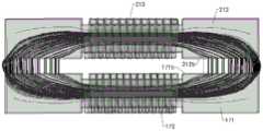
一种可选的实施例中,接收磁棒包括依次连接的第一接收端部、中部以及第二接收端部。示例性的,接收磁棒大致呈长方柱状。接收磁棒的中部相对第一接收端部和第二接收端部内凹,以在接收磁棒的中部的周边形成凹陷空间。接收线圈可位于凹陷空间,使得接收磁棒与接收线圈组装后的结构的体积较小。其中,接收线圈绕中部的延伸方向缠绕,中部的延伸方向即为其连接第一接收端部的一端向连接第二接收端部的一端延伸的方向。In an optional embodiment, the receiving magnet bar includes a first receiving end portion, a middle portion, and a second receiving end portion that are connected in sequence. Exemplarily, the receiving magnet bar is substantially rectangular. The middle portion of the receiving magnet bar is concave relative to the first receiving end portion and the second receiving end portion to form a concave space around the middle portion of the receiving magnet bar. The receiving coil can be located in the concave space, so that the volume of the structure assembled with the receiving magnet bar and the receiving coil is small. Wherein, the receiving coil is wound around the extending direction of the middle portion, and the extending direction of the middle portion is the direction in which the end connected to the first receiving end portion extends toward the end connecting to the second receiving end portion.
一种可选的实施例中,第一接收端部包括端面以及环绕地依次连接于端面周缘的第一侧面、第二侧面、第三侧面以及第四侧面。第一接收端部的第一侧面与第三侧面相背设置,第二侧面与第四侧面相背设置。第一接收端部的第二侧面的面积大于第一侧面的面积。第二接收端部包括端面以及环绕地依次连接于端面周缘的第一侧面、第二侧面、第三侧面以及第四侧面。第二接收端部的第一侧面与第三侧面相背设置,第二侧面与第四侧面相背设置。第一接收端部的第二侧面的面积大于第一侧面的面积。In an optional embodiment, the first receiving end portion includes an end surface and a first side surface, a second side surface, a third side surface and a fourth side surface that are circumferentially connected to the periphery of the end surface in sequence. The first side surface of the first receiving end is arranged opposite to the third side surface, and the second side surface is arranged opposite to the fourth side surface. The area of the second side of the first receiving end is greater than the area of the first side. The second receiving end portion includes an end surface and a first side surface, a second side surface, a third side surface and a fourth side surface that are circumferentially connected to the periphery of the end surface in sequence. The first side surface of the second receiving end is arranged opposite to the third side surface, and the second side surface is arranged opposite to the fourth side surface. The area of the second side of the first receiving end is greater than the area of the first side.
第二接收端部的第一侧面与第一接收端部的第一侧面朝向相同,第二接收端部的第二侧面与第一接收端部的第二侧面朝向相同。示例性的,第二接收端部的第一侧面与第一接收端部的第一侧面共面,第二接收端部的第二侧面与第一接收端部的第二侧面共面。第一接收耦合面包括第一接收端部的第一侧面和第二接收端部的第一侧面。第二接收耦合面包括第一接收端部的第二侧面和第二接收端部的第二侧面。The first side surface of the second receiving end portion faces the same as the first side surface of the first receiving end portion, and the second side surface of the second receiving end portion faces the same as the second side surface of the first receiving end portion. Exemplarily, the first side surface of the second receiving end portion is coplanar with the first side surface of the first receiving end portion, and the second side surface of the second receiving end portion is coplanar with the second side surface of the first receiving end portion. The first receiving coupling surface includes a first side surface of the first receiving end portion and a first side surface of the second receiving end portion. The second receiving coupling surface includes a second side surface of the first receiving end portion and a second side surface of the second receiving end portion.
一种可选的实施例中,发射磁棒包括依次连接的第一发射端部、中部以及第二发射端部。示例性的,发射磁棒大致呈长方柱状。发射磁棒的中部相对第一发射端部和第二发射端部内凹,以在发射磁棒的中部的周边形成凹陷空间。发射线圈可位于凹陷空间,使得发射磁棒与发射线圈组装后的结构的体积较小。其中,发射线圈绕中部的延伸方向缠绕,中部的延伸方向即为其连接第一发射端部的一端向连接及第二发射端部的一端延伸的方向。In an optional embodiment, the emitting magnet bar includes a first emitting end portion, a middle portion, and a second emitting end portion that are connected in sequence. Exemplarily, the emitting magnetic rod is substantially rectangular. The middle portion of the emitting magnet bar is concave relative to the first emitting end portion and the second emitting end portion, so as to form a concave space around the middle portion of the emitting magnet bar. The transmitting coil can be located in the concave space, so that the volume of the structure assembled with the transmitting magnetic rod and the transmitting coil is small. The transmitting coil is wound around the extending direction of the middle portion, and the extending direction of the middle portion is the direction in which the end connected to the first transmitting end portion extends toward the end connecting to the second transmitting end portion.
一种可选的实施例中,第一发射端部包括端面以及环绕地依次连接于端面周缘的第一侧面、第二侧面、第三侧面以及第四侧面。第一发射端部的第一侧面与第三侧面相背设置,第二侧面与第四侧面相背设置。第一发射端部的第二侧面和第四侧面的面积大于第一侧面和第三侧面的面积。第二发射端部包括端面以及环绕地依次连接于端面周缘的第一侧面、第二侧面、第三侧面以及第四侧面。第二发射端部的第一侧面与第三侧面相背设置,第二侧面与第四侧面相背设置。第二发射端部的第二侧面和第四侧面的面积大于第一侧面和第三侧面的面积。In an optional embodiment, the first emitting end portion includes an end surface and a first side surface, a second side surface, a third side surface and a fourth side surface that are circumferentially connected to the periphery of the end surface in sequence. The first side surface of the first emitting end is arranged opposite to the third side surface, and the second side surface and the fourth side surface are arranged opposite to each other. The areas of the second side surface and the fourth side surface of the first emitting end portion are larger than the areas of the first side surface and the third side surface. The second emitting end portion includes an end surface and a first side surface, a second side surface, a third side surface and a fourth side surface that are circumferentially connected to the periphery of the end surface in sequence. The first side surface of the second emitting end portion is arranged opposite to the third side surface, and the second side surface is arranged opposite to the fourth side surface. The areas of the second side surface and the fourth side surface of the second emitting end portion are larger than the areas of the first side surface and the third side surface.
第二发射端部的第一侧面与第一发射端部的第一侧面朝向相同,第二发射端部的第二侧面与第一发射端部的第二侧面朝向相同。示例性的,第二发射端部的第一侧面与第一发射端部的第一侧面共面,第二发射端部的第二侧面与第一发射端部的第二侧面共面。第一发射耦合面包括第一发射端部的第一侧面和第二发射端部的第一侧面。第二发射耦合面包括第一发射端部的第二侧面和第二发射端部的第二侧面。第二发射耦合面的面积大于第一发射耦合面的面积。其中,第二发射耦合面的数量可以为两个,另一个第二发射耦合面可以包括第一发射端部的第四侧面和第二发射端部的第四侧面。The first side surface of the second emitting end portion faces the same as the first side surface of the first emitting end portion, and the second side surface of the second emitting end portion faces the same as the second side surface of the first emitting end portion. Exemplarily, the first side surface of the second emitting end portion is coplanar with the first side surface of the first emitting end portion, and the second side surface of the second emitting end portion is coplanar with the second side surface of the first emitting end portion. The first emission coupling surface includes a first side surface of the first emission end portion and a first side surface of the second emission end portion. The second emission coupling surface includes a second side surface of the first emission end portion and a second side surface of the second emission end portion. The area of the second emission coupling surface is larger than that of the first emission coupling surface. The number of the second emission coupling surfaces may be two, and the other second emission coupling surface may include a fourth side surface of the first emission end portion and a fourth side surface of the second emission end portion.
无线充电系统处于第二充电模式时,充电头外壳的两个外壳侧面均可接触后盖,以实现充电。具体的,无线充电系统对接收线圈和发射线圈的极性(也即缠绕方向)没有限制,充电头外壳无需区分正反,两个外壳侧面中的任一者接触后盖后,发射线圈均可以与接收线圈相耦合,故而充电线缆任意方向连接后均能够实现充电,用户体验好。When the wireless charging system is in the second charging mode, both sides of the housing of the charging head can be in contact with the back cover for charging. Specifically, the wireless charging system has no restrictions on the polarities (that is, the winding direction) of the receiving coil and the transmitting coil, and the charging head shell does not need to distinguish between positive and negative. It is coupled with the receiving coil, so the charging cable can be charged in any direction, and the user experience is good.
一种可选的实施例中,发射磁棒采用软磁性材料制作,以获得较大的饱和磁感应强度。软磁性材料可以为但不限于为铁氧体、铁基纳米晶合金、铁基非晶合金、坡莫合金等材料。发射线圈采用铜线,线类型可以为利兹线,以减小趋肤效应、降低交流损耗。接收磁棒的材料与接收磁棒相同。接收线圈的材料与发射线圈相同。In an optional embodiment, the emitting magnetic rod is made of soft magnetic material, so as to obtain a larger saturation magnetic induction intensity. The soft magnetic material can be, but is not limited to, ferrite, iron-based nanocrystalline alloy, iron-based amorphous alloy, permalloy and other materials. The transmitting coil adopts copper wire, and the wire type can be Litz wire to reduce skin effect and AC loss. The material of the receiving magnet is the same as the receiving magnet. The material of the receiver coil is the same as that of the transmitter coil.
一种可选的实施例中,电子设备还包括绝缘层,绝缘层覆盖接收磁棒的外表面。绝缘层可采用绝缘泡棉、绝缘漆或者绝缘薄膜等。可以理解的,由于接收磁棒的电阻率很低,是良导体,若接收线圈表层的绝缘保护层出现破损、接收线圈直接接触接收磁棒,则很容易通过接收磁棒表面短路。In an optional embodiment, the electronic device further includes an insulating layer covering the outer surface of the receiving magnet bar. The insulating layer can be insulating foam, insulating paint or insulating film. It is understandable that because the resistivity of the receiving magnetic rod is very low, it is a good conductor. If the insulating protective layer on the surface of the receiving coil is damaged and the receiving coil directly contacts the receiving magnetic rod, it is easy to short-circuit through the surface of the receiving magnetic rod.
本实施例中,绝缘层的设置能够防止接收线圈通过接收磁棒发生短路,从而增加充电组件的可靠性。其中,发射磁棒的外表面也可以覆盖有绝缘层,以防止发射线圈经发射磁棒发生短路。In this embodiment, the arrangement of the insulating layer can prevent the receiving coil from short-circuiting through the receiving magnetic rod, thereby increasing the reliability of the charging assembly. Wherein, the outer surface of the emitting magnetic rod can also be covered with an insulating layer to prevent the short circuit of the emitting coil through the emitting magnetic rod.
一种可选的实施例中,电子设备还包括屏蔽罩,屏蔽罩套设于接收线圈的外侧,屏蔽罩用于屏蔽接收线圈产生的电场。此时,屏蔽罩可以在接收线圈的外侧形成法拉第笼,从而屏蔽接收线圈产生的电场,以降低接收线圈对外的电磁干扰。屏蔽罩可采用铜箔等电屏蔽材料。其中,屏蔽罩的材料采用磁导率低的材料,以使磁力线更多地在接收磁棒中传输。其中,充电端部也可以包括屏蔽罩,屏蔽罩套设于发射线圈的外侧,用于屏蔽发射线圈产生的电场。In an optional embodiment, the electronic device further includes a shielding cover, the shielding cover is sleeved on the outer side of the receiving coil, and the shielding cover is used for shielding the electric field generated by the receiving coil. At this time, the shielding cover can form a Faraday cage outside the receiving coil, so as to shield the electric field generated by the receiving coil, so as to reduce the external electromagnetic interference of the receiving coil. The shield can be made of electrical shielding materials such as copper foil. Among them, the material of the shield is made of materials with low magnetic permeability, so that more magnetic lines of force are transmitted in the receiving magnetic rod. Wherein, the charging end portion may also include a shielding cover, and the shielding cover is sleeved on the outer side of the transmitting coil for shielding the electric field generated by the transmitting coil.
一种可选的实施例中,电子设备还包括第一磁吸组件,第一磁吸组件位于边框内侧且排布于接收磁棒周边。充电线缆还包括第二磁吸组件,第二磁吸组件位于充电头外壳的内部且排布于发射磁棒的周边。无线充电系统处于第一充电模式和第二充电模式时,第一磁吸组件和第二磁吸组件彼此吸引。In an optional embodiment, the electronic device further includes a first magnetic attraction component, and the first magnetic attraction component is located inside the frame and arranged around the receiving magnet bar. The charging cable further includes a second magnetic attracting component, and the second magnetic attracting component is located inside the housing of the charging head and arranged on the periphery of the emitting magnetic rod. When the wireless charging system is in the first charging mode and the second charging mode, the first magnetic attraction component and the second magnetic attraction component attract each other.
在本申请实施例中,无线充电系统处于第一充电模式和第二充电模式时,电子设备的第一磁吸组件和充电线缆的充电端部的第二磁吸组件彼此吸引,以使充电端部靠近电子设备后能够自动对齐到预定区域,使得发射磁棒与接收磁棒对位精确,而且充电端部能够稳定地吸附在电子设备上,使得无线充电系统的充电过程的可靠性高。In the embodiment of the present application, when the wireless charging system is in the first charging mode and the second charging mode, the first magnetic component of the electronic device and the second magnetic component of the charging end of the charging cable attract each other, so that the charging After the end is close to the electronic device, it can be automatically aligned to the predetermined area, so that the transmitting magnet bar and the receiving magnet bar are accurately aligned, and the charging end can be stably attached to the electronic device, making the charging process of the wireless charging system highly reliable.
一种可选的实施例中,第一磁吸组件包括两个第一磁吸块和两个第二磁吸块,两个第一磁吸块分别排布于接收磁棒的两侧,两个第二磁吸块分别排布于接收磁棒的两侧,第一磁吸块位于边框与第二磁吸块之间。In an optional embodiment, the first magnetic attraction component includes two first magnetic attraction blocks and two second magnetic attraction blocks, and the two first magnetic attraction blocks are respectively arranged on both sides of the receiving magnet bar, and the two The second magnetic attraction blocks are respectively arranged on both sides of the receiving magnet bar, and the first magnetic attraction blocks are located between the frame and the second magnetic attraction blocks.
第二磁吸组件包括两个第三磁吸块和两个第四磁吸块,两个第三磁吸块分别排布于发射磁棒的两侧,两个第四磁吸块分别排布于发射磁棒的两侧,第三磁吸块位于外壳端面与第四磁吸块之间。The second magnetic attraction assembly includes two third magnetic attraction blocks and two fourth magnetic attraction blocks, the two third magnetic attraction blocks are respectively arranged on both sides of the emitting magnetic rod, and the two fourth magnetic attraction blocks are respectively arranged On both sides of the emitting magnet bar, the third magnetic attraction block is located between the end surface of the casing and the fourth magnetic attraction block.
无线充电系统处于第一充电模式时,两个第一磁吸块一一对应地与两个第三磁吸块彼此吸引。无线充电系统处于第二充电模式时,两个第一磁吸块一一对应地与两个第四磁吸块彼此吸引,两个第二磁吸块一一对应地与两个第三磁吸块彼此吸引。When the wireless charging system is in the first charging mode, the two first magnetic attraction blocks and the two third magnetic attraction blocks attract each other in a one-to-one correspondence. When the wireless charging system is in the second charging mode, the two first magnetic attraction blocks and the two fourth magnetic attraction blocks attract each other in a one-to-one correspondence, and the two second magnetic attraction blocks are in a one-to-one correspondence with the two third magnetic attraction blocks. Blocks attract each other.
在本实施例中,由于两个第一磁吸块与两个第三磁吸块能够彼此吸引,使得充电端部被吸附在电子设备的边框的充电区域处,发射磁棒与接收磁棒对位准确,充电端部的外壳端面稳定且定位准确地接触边框的充电区域,从而保证发射线圈与接收线圈的耦合效果,使得无线充电系统在第一充电模式时的充电过程可靠。In this embodiment, since the two first magnetic attraction blocks and the two third magnetic attraction blocks can attract each other, the charging end is adsorbed at the charging area of the frame of the electronic device, and the transmitting magnetic bar and the receiving magnetic bar are opposite to each other. The position is accurate, and the end face of the shell of the charging end is stable and accurately positioned to contact the charging area of the frame, thereby ensuring the coupling effect of the transmitting coil and the receiving coil, and making the charging process of the wireless charging system in the first charging mode reliable.
由于两个第一磁吸块与两个第四磁吸块能够彼此吸引,两个第二磁吸块与两个第三磁吸块能够彼此吸引,使得充电端部被吸附在电子设备的后盖的充电区域处,使得发射磁棒与接收磁棒对位准确,充电端部的外壳端面稳定且定位准确地接触后盖的充电区域,从而保证发射线圈与接收线圈的耦合效果,使得无线充电系统在第一充电模式时的充电过程可靠。Since the two first magnetic blocks and the two fourth magnetic blocks can attract each other, the two second magnetic blocks and the two third magnetic blocks can attract each other, so that the charging end is attracted to the rear of the electronic device At the charging area of the cover, the transmitting magnetic rod and the receiving magnetic rod are accurately aligned, and the end face of the shell of the charging end is stably and accurately positioned to contact the charging area of the back cover, so as to ensure the coupling effect of the transmitting coil and the receiving coil, making wireless charging The charging process of the system in the first charging mode is reliable.
一种可选的实施例中,充电组件还包括固定件。固定件用于将接收磁棒固定于边框内侧。其中,固定件采用非铁磁材料,以防止无线充电电磁场从固定件通过,从而降低对无线充电效率的影响。非铁磁材料可以为但不限于为奥氏体不锈钢。In an optional embodiment, the charging assembly further includes a fixing member. The fixing piece is used to fix the receiving magnetic rod on the inner side of the frame. Wherein, the fixing member adopts non-ferromagnetic material to prevent the wireless charging electromagnetic field from passing through the fixing member, thereby reducing the influence on the wireless charging efficiency. The non-ferromagnetic material may be, but is not limited to, austenitic stainless steel.
其他实施例中,也可以通过点胶方式将接收磁棒固定于边框内侧。例如,通过粘接件将接收磁棒粘接至边框、中板或后盖。或者,通过粘接件将固定接收磁棒的中间结构件粘接至边框、中板或后盖,从而固定接收磁棒。In other embodiments, the receiving magnetic rod can also be fixed on the inner side of the frame by dispensing glue. For example, the receiving magnet bar is bonded to the frame, the mid-board or the back cover by means of an adhesive. Alternatively, the intermediate structural member for fixing and receiving the magnetic bar is bonded to the frame, the middle plate or the back cover through an adhesive member, so as to fix the receiving magnetic bar.
一种可选的实施例中,边框包括第一框部和与第一框部相交的第二框部。接收磁棒的数量为至少两个,其中一个接收磁棒的第一接收耦合面面向第一框部,另一个接收磁棒的第一接收耦合面面向第二框部。接收线圈的数量与接收磁棒的数量相同,至少两个接收线圈一一对应地缠绕于至少两个接收磁棒,所有的接收线圈均电连接电池。In an optional embodiment, the frame includes a first frame portion and a second frame portion intersecting with the first frame portion. The number of receiving magnetic bars is at least two, wherein the first receiving coupling surface of one receiving magnetic bar faces the first frame portion, and the first receiving coupling surface of the other receiving magnetic bar faces the second frame portion. The number of receiving coils is the same as the number of receiving magnetic bars, at least two receiving coils are wound around at least two receiving magnetic bars in one-to-one correspondence, and all receiving coils are electrically connected to the battery.
在本实施例中,电子设备具有对应于多个接收磁棒的多个充电位置,用户可以依据竖屏握持或横屏握持的需求,灵活地选择充电位置,从而在多种场景下实现边充边玩,电子设备的无线充电体验更佳。In this embodiment, the electronic device has multiple charging positions corresponding to multiple receiving magnetic bars, and the user can flexibly select the charging position according to the requirements of holding the vertical screen or holding the horizontal screen, so as to realize the realization in various scenarios. Play while charging, and the wireless charging experience of electronic devices is better.
一种可选的实施例中,电子设备还包括接收匹配电路、无线充电接收控制芯片、一级变换器、二级变换器以及充电控制芯片,接收线圈、接收匹配电路、无线充电接收控制芯片、一级变换器、二级变换器、充电控制芯片以及电池依次连接。无线充电系统处于第一充电模式时,一级变换器处于旁路模式,二级变换器实现降压;无线充电系统处于第二充电模式时,一级变换器实现一级降压,二级变换器实现二级降压。In an optional embodiment, the electronic device further includes a receiving matching circuit, a wireless charging receiving control chip, a primary converter, a secondary converter and a charging control chip, a receiving coil, a receiving matching circuit, a wireless charging receiving control chip, The primary converter, the secondary converter, the charging control chip and the battery are connected in sequence. When the wireless charging system is in the first charging mode, the first-level converter is in the bypass mode, and the second-level converter realizes step-down; when the wireless charging system is in the second charging mode, the first-level converter realizes the first-level step-down and the second-level converter The device achieves a secondary step-down.
在本实施例中,由于第一充电模式的充电速度较慢,因此电压转换器通过一次降压将无线充电接收控制芯片输出的直流电压降低至预定范围内,而第二充电模式的充电速度较快,因此电压转换器通过连续的二次降压将无线充电接收控制芯片输出的直流电压降低至预定范围内,故而电压转换器的降压范围广,电子设备能够适用于多种充电模式。In this embodiment, since the charging speed of the first charging mode is relatively slow, the voltage converter reduces the DC voltage output by the wireless charging receiving control chip to a predetermined range through a step-down, while the charging speed of the second charging mode is faster than that in the second charging mode. Therefore, the voltage converter reduces the DC voltage output by the wireless charging receiver control chip to a predetermined range through continuous secondary step-down, so the voltage converter has a wide step-down range, and the electronic device can be applied to various charging modes.
一种可选的实施例中,充电线缆包括依次连接的充电端部、线缆部以及适配器端部。充电端部包括前述充电头外壳、前述发射磁棒以及前述发射线圈。线缆部可以移动和变形。充电端部用于可拆卸地搭接于电子设备,从而与电子设备相耦合,以传输能量和信号。线缆部用于在充电端部与适配器端部之间传输能量和信号。适配器端部用于可拆卸地插接电源适配器或电源。In an optional embodiment, the charging cable includes a charging end portion, a cable portion, and an adapter end portion that are connected in sequence. The charging end includes the aforementioned charging head housing, the aforementioned transmitting magnetic rod, and the aforementioned transmitting coil. The cable portion can move and deform. The charging end is used to be detachably attached to the electronic device so as to be coupled with the electronic device to transmit energy and signals. The cable portion is used to transfer energy and signals between the charging end and the adapter end. The adapter end is used to removably plug the power adapter or power supply.
一种可选的实施例中,适配器端部包括升压电路,升压电路经线缆部电连接发射线圈。由于充电线缆的适配器端部设有升压电路,因此若适配器端部连接至不支持调压功能的电源适配器(例如老的电源适配器只支持5V的输出,不支持升压)时,升压电路能够实现调压功能,使得充电线缆的发射功率满足多种充电模式的需求,故而充电线缆的兼容性更好。In an optional embodiment, the end of the adapter includes a booster circuit, and the booster circuit is electrically connected to the transmitting coil through the cable portion. Since the adapter end of the charging cable is equipped with a boost circuit, if the adapter end is connected to a power adapter that does not support voltage regulation (for example, the old power adapter only supports 5V output and does not support boost), the boost will The circuit can realize the voltage regulation function, so that the transmission power of the charging cable can meet the requirements of various charging modes, so the compatibility of the charging cable is better.
此外,由于升压电路位于充电线缆的适配器端部,充电线缆的其他主要硬件电路位于充电端部,也即升压电路与其他硬件电路分别位于充电线缆的两端,在物理上实现隔离,从而能够将容易发热的升压电路与其他热源分散开,以防止充电线缆的局部温度过高。In addition, since the booster circuit is located at the adapter end of the charging cable, other main hardware circuits of the charging cable are located at the charging end, that is, the booster circuit and other hardware circuits are located at both ends of the charging cable, which is physically realized isolation, so that the heat-prone boost circuit can be separated from other heat sources to prevent the local temperature of the charging cable from being too high.
一种可选的实施例中,无线充电系统还可以包括电源适配器。电源适配器用于将高压交流电转换成低压直流电。充电线缆的适配器端部用于可拆卸地插接电源适配器。此时,充电线缆能够将低压直流电转换成低压交流电,以耦合至电子设备。电源适配器插入电源插座后,电源插座中电量可通过电源适配器和充电线缆传输给电子设备,以对电子设备进行充电。In an optional embodiment, the wireless charging system may further include a power adapter. The power adapter is used to convert high voltage alternating current to low voltage direct current. The adapter end of the charging cable is used to detachably plug in the power adapter. At this point, the charging cable can convert the low-voltage direct current to low-voltage alternating current for coupling to the electronic device. After the power adapter is inserted into the power socket, the power in the power socket can be transmitted to the electronic device through the power adapter and the charging cable, so as to charge the electronic device.
另一种可选的实施例中,适配器端部还可以用于可拆卸地插接充电宝等电源,电源通过充电线缆对电子设备进行充电。示例性的,某些携带电池的电子设备(例如笔记本电脑)也可以作为电源,为待充电的电子设备供电。In another optional embodiment, the end of the adapter can also be used to detachably plug in a power source such as a power bank, and the power source charges the electronic device through a charging cable. Exemplarily, some electronic devices (such as notebook computers) that carry batteries can also be used as power sources to supply power to the electronic devices to be charged.
第二方面,本申请实施例还提供一种电子设备。电子设备包括边框、后盖、接收磁棒、接收线圈以及电池,边框环绕地连接于后盖的周缘,接收磁棒位于边框内侧,接收磁棒包括第一接收耦合面和与第一接收耦合面相交的第二接收耦合面,第二接收耦合面的面积大于第一接收耦合面的面积,第一接收耦合面面向边框设置,第二接收耦合面面向后盖设置,接收线圈缠绕于接收磁棒的中部,电池位于边框内侧且电连接接收线圈。In a second aspect, the embodiments of the present application further provide an electronic device. The electronic device includes a frame, a back cover, a receiving magnetic rod, a receiving coil and a battery, the frame is connected to the periphery of the back cover in a surrounding manner, the receiving magnetic rod is located inside the frame, and the receiving magnetic rod includes a first receiving coupling surface and a first receiving coupling surface. The intersecting second receiving coupling surface, the area of the second receiving coupling surface is larger than the area of the first receiving coupling surface, the first receiving coupling surface is disposed facing the frame, the second receiving coupling surface is disposed facing the back cover, the receiving coil is wound around the receiving magnetic rod In the middle of the frame, the battery is located inside the frame and is electrically connected to the receiving coil.
接收线圈用于在第一充电模式中,经第一接收耦合面与充电线缆的发射线圈相耦合且耦合系数为第一耦合系数。接收线圈还用于在第二充电模式中,经第二接收耦合面与充电线缆的发射线圈相耦合且耦合系数为第二耦合系数,第二耦合系数大于第一耦合系数。The receiving coil is used for coupling with the transmitting coil of the charging cable through the first receiving coupling surface in the first charging mode, and the coupling coefficient is the first coupling coefficient. The receiving coil is also used to couple with the transmitting coil of the charging cable through the second receiving coupling surface in the second charging mode, and the coupling coefficient is a second coupling coefficient, and the second coupling coefficient is greater than the first coupling coefficient.
在本实施例中,电子设备通过充电线缆进行充电,由于充电线缆体积小、重量轻,充电线缆可以移动和变形,因此充电线缆能够随电子设备移动,使得用户能够在电子设备进行无线充电时握持和使用电子设备,实现边充边玩,从而提高了电子设备在无线充电场景下的用户使用体验。In this embodiment, the electronic device is charged through a charging cable. Since the charging cable is small in size and light in weight, the charging cable can be moved and deformed, so the charging cable can move with the electronic device, so that the user can Holding and using the electronic device during wireless charging can realize playing while charging, thereby improving the user experience of the electronic device in the wireless charging scenario.
充电线缆的发射线圈的磁力线既可以耦合到接收磁棒的第一接收耦合面,以在第一充电模式下对电子设备进行充电,发射线圈的磁力线也可以耦合到接收磁棒的第二接收耦合面,以在第二充电模式下对电子设备进行充电,因此电子设备具有两种充电模式,两种充电模式下充电线缆连接电子设备的方式不同,故而电子设备的充电方式更为多样化,有利于无线充电的多场景覆盖,使得电子设备的无线充电体验更佳。The magnetic lines of force of the transmitting coil of the charging cable can be coupled to the first receiving coupling surface of the receiving magnetic rod to charge the electronic device in the first charging mode, and the magnetic lines of force of the transmitting coil can also be coupled to the second receiving surface of the receiving magnetic rod. The coupling surface is used to charge the electronic device in the second charging mode. Therefore, the electronic device has two charging modes. In the two charging modes, the charging cable is connected to the electronic device in different ways, so the charging methods of the electronic device are more diverse. , which is conducive to the multi-scenario coverage of wireless charging, making the wireless charging experience of electronic devices better.
由于第二耦合系数大于第一耦合系数,电子设备在第二充电模式下的充电速度比在第一充电模式下的充电速度更快,第一充电模式对应于普通充电,第二充电模式对应于快速充电,以实现无线充电的多场景模式覆盖。用户能够依据其具体需求,灵活的选择电子设备的充电速度,使得电子设备的无线充电体验更佳。例如,普通充电相较于快速充电,由于其充电功率低,可以延长电子设备的电池的循环寿命,从而减轻电池的容量退化问题,所以在时间宽松的情况下(例如晚上睡觉),用户可以选择普通充电,在时间较为仓促时(例如急需出门),用户可以选择快速充电。Since the second coupling coefficient is greater than the first coupling coefficient, the charging speed of the electronic device in the second charging mode is faster than that in the first charging mode, the first charging mode corresponds to the normal charging, and the second charging mode corresponds to Fast charging for multi-scene mode coverage of wireless charging. Users can flexibly select the charging speed of the electronic device according to their specific needs, so that the wireless charging experience of the electronic device is better. For example, compared with fast charging, ordinary charging can prolong the cycle life of the battery of electronic devices due to its low charging power, thereby reducing the capacity degradation problem of the battery. Therefore, in the case of loose time (such as sleeping at night), users can choose Ordinary charging, when the time is relatively short (for example, when you need to go out urgently), users can choose fast charging.
此外,由于充电端部搭接在电子设备上即可对电子设备充电,无需在电子设备上开设凹陷的插接端口并在插接端口内设置外露的连接端子,因此电子设备的外观一致性更佳,密封性能更好,也能够避免发生因连接端子老化或变形而导致电子设备充电慢、无法充电等问题。In addition, since the charging end is overlapped on the electronic device to charge the electronic device, there is no need to open a recessed plug port on the electronic device and set exposed connection terminals in the plug port, so the appearance of the electronic device is more consistent. It has better sealing performance, and can also avoid problems such as slow charging and inability to charge electronic devices due to aging or deformation of connecting terminals.
此外,电子设备为满足轻薄化和大屏显示需求,宽度方向的尺寸及长度方向的尺寸较大,而厚度方向的尺寸较小。本实施例中,接收磁棒的第一接收端部、中部及第二接收端部的排列方向平行于电子设备的宽度方向,面向边框的第一接收耦合面的面积小于面向后盖的第二接收耦合面的面积,因此接收磁棒在电子设备的厚度方向上的尺寸小于在电子设备的长度方向上的尺寸,使得接收磁棒充分利用电子设备的内部空间,既能够设置有面积较大的耦合面,以获得较快的充电速度,还能避免增加电子设备的厚度。In addition, in order to meet the requirements of thinning and large-screen display, electronic devices have larger dimensions in the width direction and length direction, but smaller dimensions in the thickness direction. In this embodiment, the arrangement direction of the first receiving end portion, the middle portion and the second receiving end portion of the receiving magnet bar is parallel to the width direction of the electronic device, and the area of the first receiving coupling surface facing the frame is smaller than that of the second receiving end facing the back cover. The area of the receiving coupling surface, so the size of the receiving magnetic bar in the thickness direction of the electronic device is smaller than the size in the length direction of the electronic device, so that the receiving magnetic bar can make full use of the internal space of the electronic device. Coupling surface to obtain faster charging speed and avoid increasing the thickness of electronic equipment.
一种可选的实施例中,电子设备还包括第一磁吸组件,第一磁吸组件位于边框内侧且排布于接收磁棒周边,第一磁吸组件用于在第一充电模式和第二充电模式中,与充电线缆的第二磁吸组件彼此吸引。In an optional embodiment, the electronic device further includes a first magnetic attraction component, the first magnetic attraction component is located inside the frame and is arranged around the receiving magnet bar, and the first magnetic attraction component is used in the first charging mode and the second charging mode. In the second charging mode, the second magnetic attraction component of the charging cable attracts each other.
在本申请实施例中,在第一充电模式和第二充电模式中,电子设备的第一磁吸组件和充电线缆的充电端部的第二磁吸组件彼此吸引,以使充电线缆的充电头外壳靠近电子设备后能够自动对齐到预定区域,使得发射磁棒与接收磁棒对位精确,而且充电头外壳能够稳定地吸附在电子设备上,使得充电过程的可靠性高。In the embodiment of the present application, in the first charging mode and the second charging mode, the first magnetic attraction component of the electronic device and the second magnetic attraction component of the charging end of the charging cable are attracted to each other, so that the charging cable is attracted to each other. The housing of the charging head can be automatically aligned to a predetermined area after being close to the electronic device, so that the positioning of the transmitting magnet bar and the receiving magnetic bar is accurate, and the housing of the charging head can be stably attached to the electronic device, so that the reliability of the charging process is high.
一种可选的实施例中,边框包括第一框部和与第一框部相交的第二框部。接收磁棒的数量为至少两个,其中一个接收磁棒的第一接收耦合面面向第一框部,另一个接收磁棒的第一接收耦合面面向第二框部。接收线圈的数量与接收磁棒的数量相同,至少两个接收线圈一一对应地缠绕于至少两个接收磁棒,所有的接收线圈均电连接电池。In an optional embodiment, the frame includes a first frame portion and a second frame portion intersecting with the first frame portion. The number of receiving magnetic bars is at least two, wherein the first receiving coupling surface of one receiving magnetic bar faces the first frame portion, and the first receiving coupling surface of the other receiving magnetic bar faces the second frame portion. The number of receiving coils is the same as the number of receiving magnetic bars, at least two receiving coils are wound around at least two receiving magnetic bars in one-to-one correspondence, and all receiving coils are electrically connected to the battery.
在本实施例中,电子设备具有对应于多个接收磁棒的多个充电位置,用户可以依据竖屏握持或横屏握持的需求,灵活地选择充电位置,从而在多种场景下实现边充边玩,电子设备的无线充电体验更佳。In this embodiment, the electronic device has multiple charging positions corresponding to multiple receiving magnetic bars, and the user can flexibly select the charging position according to the requirements of holding the vertical screen or holding the horizontal screen, so as to realize the realization in various scenarios. Play while charging, and the wireless charging experience of electronic devices is better.
一种可选的实施例中,电子设备还包括接收匹配电路、无线充电接收控制芯片、一级变换器、二级变换器以及充电控制芯片,接收线圈、接收匹配电路、无线充电接收控制芯片、一级变换器、二级变换器、充电控制芯片以及电池依次连接。电子设备处于第一充电模式时,一级变换器处于旁路模式,二级变换器实现降压;电子设备处于第二充电模式时,一级变换器实现一级降压,二级变换器实现二级降压。In an optional embodiment, the electronic device further includes a receiving matching circuit, a wireless charging receiving control chip, a primary converter, a secondary converter and a charging control chip, a receiving coil, a receiving matching circuit, a wireless charging receiving control chip, The primary converter, the secondary converter, the charging control chip and the battery are connected in sequence. When the electronic device is in the first charging mode, the first-level converter is in the bypass mode, and the second-level converter realizes step-down; when the electronic device is in the second charging mode, the first-level converter realizes the first-level step-down, and the second-level converter realizes the step-down Secondary buck.
在本实施例中,由于第一充电模式的充电速度较慢,因此电压转换器通过一次降压将无线充电接收控制芯片输出的直流电压降低至预定范围内,而第二充电模式的充电速度较快,因此电压转换器通过连续的二次降压将无线充电接收控制芯片输出的直流电压降低至预定范围内,故而电压转换器的降压范围广,电子设备能够适用于多种充电模式。In this embodiment, since the charging speed of the first charging mode is relatively slow, the voltage converter reduces the DC voltage output by the wireless charging receiving control chip to a predetermined range through a step-down, while the charging speed of the second charging mode is faster than that in the second charging mode. Therefore, the voltage converter reduces the DC voltage output by the wireless charging receiver control chip to a predetermined range through continuous secondary step-down, so the voltage converter has a wide step-down range, and the electronic device can be applied to various charging modes.
第三方面,本申请实施例还提供一种充电线缆。充电线缆包括充电头外壳、发射磁棒以及发射线圈,充电头外壳包括外壳端面和连接于外壳端面周缘的外壳侧面,发射磁棒位于充电头外壳的内部,发射磁棒包括第一发射耦合面和与第一发射耦合面相交的第二发射耦合面,第二发射耦合面的面积大于第一发射耦合面的面积,第一发射耦合面面向外壳端面,第二发射耦合面面向外壳侧面,发射线圈缠绕于发射磁棒的中部。In a third aspect, an embodiment of the present application further provides a charging cable. The charging cable includes a charging head casing, a transmitting magnetic rod and a transmitting coil. The charging head casing includes an end surface of the casing and a side surface of the casing connected to the periphery of the end face of the casing. The transmitting magnetic rod is located inside the charging head casing, and the transmitting magnetic rod includes a first transmitting coupling surface. and the second emission coupling surface intersecting with the first emission coupling surface, the area of the second emission coupling surface is larger than that of the first emission coupling surface, the first emission coupling surface faces the end face of the housing, the second emission coupling surface faces the side surface of the housing, and the emission The coil is wound around the middle of the emitting magnet bar.
发射线圈用于在第一充电模式中,经第一发射耦合面与电子设备的接收线圈相耦合且耦合系数为第一耦合系数。发射线圈还用于在第二充电模式中,经第二发射耦合面与电子设备的接收线圈相耦合且耦合系数为第二耦合系数,第二耦合系数大于第一耦合系数。The transmitting coil is used to couple with the receiving coil of the electronic device through the first transmitting coupling surface in the first charging mode, and the coupling coefficient is the first coupling coefficient. The transmitting coil is also used to couple with the receiving coil of the electronic device through the second transmitting coupling surface in the second charging mode, and the coupling coefficient is the second coupling coefficient, and the second coupling coefficient is greater than the first coupling coefficient.
在本实施例中,通过充电线缆对电子设备进行充电,由于充电线缆体积小、重量轻,充电线缆可以移动和变形,因此充电线缆能够随电子设备移动,使得用户能够在电子设备进行无线充电时握持和使用电子设备,实现边充边玩,从而提高了电子设备在无线充电场景下的用户使用体验,使得充电线缆的使用范围更广。同时,无线充电系统的充电线缆作为电子设备的充电装置,相较于传统的无线充电底座(具有扁平的发射线圈),体积更为小巧,易于携带。In this embodiment, the electronic device is charged through the charging cable. Since the charging cable is small in size and light in weight, the charging cable can be moved and deformed, so the charging cable can move with the electronic device, so that the user can Holding and using the electronic device during wireless charging realizes playing while charging, thereby improving the user experience of the electronic device in the wireless charging scenario and making the charging cable more widely used. At the same time, the charging cable of the wireless charging system, as a charging device for electronic devices, is smaller in size and easier to carry than a traditional wireless charging base (with a flat transmitting coil).
充电线缆的发射磁棒的磁力线既可以通过第一发射耦合面耦合到电子设备的接收线圈,以在第一充电模式下对电子设备进行充电,发射磁棒的磁力线也可以通过第二发射耦合面、耦合到电子设备的接收线圈,以在第二充电模式下对电子设备进行充电,因此充电线缆具有两种充电模式,两种充电模式下充电线缆连接电子设备的方式不同,故而充电线缆对电子设备的充电方式更为多样化,有利于无线充电的多场景覆盖,提高无线充电体验。The magnetic field lines of the emitting magnet bar of the charging cable can be coupled to the receiving coil of the electronic device through the first emitting coupling surface to charge the electronic device in the first charging mode, and the magnetic field lines of the emitting magnet bar can also be coupled through the second emitting coupling surface, coupled to the receiving coil of the electronic device to charge the electronic device in the second charging mode, so the charging cable has two charging modes. The charging methods of cables to electronic devices are more diverse, which is conducive to the multi-scenario coverage of wireless charging and improves the wireless charging experience.
充电头外壳大致呈扁平状结构,发射磁棒的形状与充电头外壳的形状相似,且安装于充电头外壳的内部时,其面积较小的面(也即第一发射耦合面)与充电头外壳的外壳端面正对,其面积较大的面(也即第二发射耦合面)与充电头外壳的外壳侧面正对,以充分利用充电头外壳的内部空间,从而既能够设置有面积较大的耦合面,以获得较快的充电速度,还能避免明显增加充电头外壳的体积。The shell of the charging head is generally in a flat structure, and the shape of the emitting magnetic rod is similar to that of the shell of the charging head. The end face of the shell of the shell is facing, and the larger surface (that is, the second emission coupling surface) is facing the side of the shell of the charging head shell, so as to make full use of the inner space of the charging head shell, so that both a larger area can be set. The coupling surface can be used to obtain a faster charging speed, and it can also avoid significantly increasing the volume of the charging head shell.
一种可选的实施例中,充电线缆还包括第二磁吸组件,第二磁吸组件位于充电头外壳的内部且排布于发射磁棒的周边;第二磁吸组件用于在第一充电模式和第二充电模式中,与电子设备的第一磁吸组件彼此吸引。In an optional embodiment, the charging cable further includes a second magnetic attraction component, the second magnetic attraction component is located inside the housing of the charging head and is arranged on the periphery of the launching magnet bar; the second magnetic attraction component is used for In the first charging mode and the second charging mode, the first magnetic attraction component of the electronic device is attracted to each other.
在本申请实施例中,在第一充电模式和第二充电模式中,电子设备的第一磁吸组件和充电线缆的充电端部的第二磁吸组件彼此吸引,以使充电线缆的充电头外壳靠近电子设备后能够自动对齐到预定区域,使得发射磁棒与接收磁棒对位精确,而且充电头外壳能够稳定地吸附在电子设备上,使得充电过程的可靠性高。In the embodiment of the present application, in the first charging mode and the second charging mode, the first magnetic attraction component of the electronic device and the second magnetic attraction component of the charging end of the charging cable are attracted to each other, so that the charging cable is attracted to each other. The housing of the charging head can be automatically aligned to a predetermined area after being close to the electronic device, so that the positioning of the transmitting magnet bar and the receiving magnetic bar is accurate, and the housing of the charging head can be stably attached to the electronic device, so that the reliability of the charging process is high.
一种可选的实施例中,充电线缆包括依次连接的充电端部、线缆部以及适配器端部,充电端部包括充电头外壳、发射磁棒以及发射线圈,适配器端部包括升压电路,升压电路经线缆部电连接发射线圈。In an optional embodiment, the charging cable includes a charging end, a cable and an adapter end connected in sequence, the charging end includes a charging head shell, a transmitting magnetic rod and a transmitting coil, and the adapter end includes a booster circuit. , the booster circuit is electrically connected to the transmitting coil through the cable part.
在本实施例中,由于充电线缆的适配器端部设有升压电路,因此若适配器端部连接至不支持调压功能的电源适配器(例如老的电源适配器只支持5V的输出,不支持升压)时,升压电路能够实现调压功能,使得充电线缆的发射功率满足多种充电模式的需求,故而充电线缆的兼容性更好。In this embodiment, since the end of the adapter of the charging cable is provided with a booster circuit, if the end of the adapter is connected to a power adapter that does not support voltage regulation (for example, the old power adapter only supports 5V output and does not support boosting When the voltage is increased), the boost circuit can realize the voltage regulation function, so that the transmission power of the charging cable can meet the requirements of various charging modes, so the compatibility of the charging cable is better.
此外,由于升压电路位于充电线缆的适配器端部,充电线缆的其他主要硬件电路位于充电端部,也即升压电路与其他硬件电路分别位于充电线缆的两端,在物理上实现隔离,从而能够将容易发热的升压电路与其他热源分散开,以防止充电线缆的局部温度过高。In addition, since the booster circuit is located at the adapter end of the charging cable, other main hardware circuits of the charging cable are located at the charging end, that is, the booster circuit and other hardware circuits are located at both ends of the charging cable, which is physically realized isolation, so that the heat-prone boost circuit can be separated from other heat sources to prevent the local temperature of the charging cable from being too high.
第四方面,本申请实施例还提供一种电子设备的无线充电方法。无线充电方法可以应用于前述电子设备中。In a fourth aspect, an embodiment of the present application further provides a wireless charging method for an electronic device. The wireless charging method can be applied to the aforementioned electronic devices.
无线充电方法包括:Wireless charging methods include:
电子设备接收充电线缆发射的数字通信信号并回复确认信号;The electronic device receives the digital communication signal transmitted by the charging cable and replies with the confirmation signal;
电子设备判断是否处于第一充电模式或第二充电模式;The electronic device determines whether it is in the first charging mode or the second charging mode;
若电子设备处于第一充电模式,则电子设备向充电线缆传输第一调节信号,以使充电线缆依据第一调节信号调节发射线圈的电气参数后对电子设备进行普通充电;If the electronic device is in the first charging mode, the electronic device transmits a first adjustment signal to the charging cable, so that the charging cable adjusts the electrical parameters of the transmitting coil according to the first adjustment signal and then performs normal charging on the electronic device;
若电子设备处于第二充电模式,则电子设备向充电线缆传输第二调节信号,以使充电线缆依据第二调节信号调节发射线圈的电气参数后对电子设备进行快速充电。If the electronic device is in the second charging mode, the electronic device transmits a second adjustment signal to the charging cable, so that the charging cable adjusts the electrical parameters of the transmitting coil according to the second adjustment signal to quickly charge the electronic device.
在本实施例中,充电线缆能够依据电子设备传输的调节信号动态调节其发射线圈的电气参数,从而在对应的充电模式下,调节接收线圈的接收功率,以调整无线充电功率至需求功率,从而稳定地向电子设备传输能量,使得无线充电系统的充电过程的可靠性高。In this embodiment, the charging cable can dynamically adjust the electrical parameters of its transmitting coil according to the adjustment signal transmitted by the electronic device, so as to adjust the receiving power of the receiving coil in the corresponding charging mode, so as to adjust the wireless charging power to the required power, Therefore, energy is stably transmitted to the electronic device, so that the reliability of the charging process of the wireless charging system is high.
其中,电子设备的无线充电接收控制芯片可以依据电源管理模块传输的输入调节信号调制出第一调节信号或第二调节信号,并采用幅移键控调制方式,将第一调节信号或第二调节信号通过接收线圈耦合至充电端部的发射线圈,从而实现传输。充电端部的无线充电发射控制芯片能够解调第一调节信号或第二调节信号,以获得调节信息,然后依据调节信息调节发射线圈的电气参数,从而调节接收线圈的接收功率和无线充电系统的无线充电功率,以满足当前充电模式的充电功率需求。Among them, the wireless charging receiving control chip of the electronic device can modulate the first adjustment signal or the second adjustment signal according to the input adjustment signal transmitted by the power management module, and adopt the amplitude shift keying modulation method to adjust the first adjustment signal or the second adjustment signal. The signal is coupled to the transmitter coil at the charging end through the receiver coil to achieve transmission. The wireless charging transmission control chip at the charging end can demodulate the first adjustment signal or the second adjustment signal to obtain adjustment information, and then adjust the electrical parameters of the transmitting coil according to the adjustment information, thereby adjusting the receiving power of the receiving coil and the wireless charging system. Wireless charging power to meet the charging power requirements of the current charging mode.
一种实施例中,可通过定频调压方案实现无线充电功率调节。也即,固定发射线圈中交流电的频率,调整发射线圈中交流电的电压。具体的,第一调节信号和第二调节信号为调压信号,无线充电发射控制芯片解调第一调节信号或第二调节信号后获得的调节信息为调压信息。其中,调节信号可以携带升高或降低至某个需求电压信息的信号。In one embodiment, the wireless charging power regulation can be realized through a fixed-frequency voltage regulation scheme. That is, the frequency of the alternating current in the transmitting coil is fixed, and the voltage of the alternating current in the transmitting coil is adjusted. Specifically, the first adjustment signal and the second adjustment signal are voltage adjustment signals, and the adjustment information obtained after the wireless charging and transmission control chip demodulates the first adjustment signal or the second adjustment signal is the voltage adjustment information. Among them, the adjustment signal may carry a signal that increases or decreases to a certain demand voltage information.
一种示例中,电源适配器具有调压功能。无线充电发射控制芯片形成调压信息后,将调压信息通过线缆部、适配器端部传输给电源适配器的接口控制器,接口控制器将调压信息反馈给单端反激电源控制器,单端反激电源控制器依据调压信息控制变压器,使得电源适配器输出的低压直流电的电压调整到需求电压,具有需求电压的低压直流电经适配器端部和线缆部传输给充电端部的无线充电发射控制芯片,无线充电发射控制芯片将具有需求电压的低压直流电转换成交流电,使得充电线缆的发射线圈上的交流电的电压发生变化,从而实现无线充电功率的调节。In one example, the power adapter has a voltage regulation function. After the wireless charging transmission control chip forms the voltage regulation information, it transmits the voltage regulation information to the interface controller of the power adapter through the cable part and the end of the adapter, and the interface controller feeds back the voltage regulation information to the single-ended flyback power supply controller. The terminal flyback power supply controller controls the transformer according to the voltage regulation information, so that the voltage of the low-voltage DC output from the power adapter is adjusted to the required voltage, and the low-voltage DC with the required voltage is transmitted to the wireless charging transmitter of the charging terminal through the adapter terminal and the cable part. The control chip, the wireless charging transmission control chip converts the low-voltage direct current with the required voltage into alternating current, so that the voltage of the alternating current on the transmitting coil of the charging cable changes, so as to realize the adjustment of the wireless charging power.
另一种示例中,电源适配器不具有调压功能,充电线缆的适配器端部具有升压电路。无线充电发射控制芯片形成调压信息后,将调压信息通过线缆部传输给适配器端部的升压电路,升压电路依据调压信息将电源适配器输出的低压直流电调整到需求电压,然后通过线缆部传输给无线充电发射控制芯片,无线充电发射控制芯片将具有需求电压的低压直流电转换成交流电,使得充电线缆的发射线圈上的交流电的电压发生变化,从而实现无线充电功率的调节。In another example, the power adapter does not have a voltage regulation function, and the adapter end of the charging cable has a boost circuit. After the wireless charging transmission control chip forms the voltage regulation information, the voltage regulation information is transmitted to the booster circuit at the end of the adapter through the cable part. The cable part is transmitted to the wireless charging transmission control chip, and the wireless charging transmission control chip converts the low-voltage direct current with the required voltage into alternating current, so that the voltage of the alternating current on the transmitting coil of the charging cable changes, so as to realize the adjustment of the wireless charging power.
另一种实施例中,可通过定压调频方案实现无线充电功率调节。也即,固定发射线圈中交流电的电压,调整发射线圈中交流电的频率。具体的,第一调节信号和第二调节信号为调频信号,无线充电发射控制芯片解调第一调节信号或第二调节信号后获得的调节信息为调频信息。其中,调频信号可以携带升高或降低至某个需求频率信息的信号。无线充电发射控制芯片获得调频信息后,可以依据调频信息直接调节其输出的交流电的频率,以调节发射线圈上的交流电的频率,从而实现无线充电功率的调节。In another embodiment, the wireless charging power adjustment can be realized through a constant voltage and frequency modulation scheme. That is, the voltage of the alternating current in the transmitting coil is fixed, and the frequency of the alternating current in the transmitting coil is adjusted. Specifically, the first adjustment signal and the second adjustment signal are frequency modulation signals, and the adjustment information obtained after the wireless charging and transmission control chip demodulates the first adjustment signal or the second adjustment signal is the frequency modulation information. Among them, the FM signal can carry a signal that is raised or lowered to a certain desired frequency information. After the wireless charging transmission control chip obtains the frequency modulation information, it can directly adjust the frequency of the output AC power according to the frequency modulation information, so as to adjust the frequency of the AC power on the transmitting coil, thereby realizing the adjustment of the wireless charging power.
再一种实施例中,可通过调占空比实现无线充电功率调节。具体的,第一调节信号和第二调节信号为调占空比信号,无线充电发射控制芯片解调第一调节信号或第二调节信号后获得的调节信息为调占空比信息。其中,调占空比信号可以携带升高或降低至某个需求占空比信息的信号。无线充电发射控制芯片获得调占空比信息后,可以依据调占空比信息直接调节其输出的交流电的占空比,以调节发射线圈上的交流电的占空比,从而实现无线充电功率的调节。In yet another embodiment, the wireless charging power adjustment can be realized by adjusting the duty cycle. Specifically, the first adjustment signal and the second adjustment signal are duty ratio adjustment signals, and the adjustment information obtained after the wireless charging and transmission control chip demodulates the first adjustment signal or the second adjustment signal is the duty cycle adjustment information. Among them, the duty cycle modulation signal may carry a signal that increases or decreases to a certain required duty cycle information. After the wireless charging transmission control chip obtains the duty cycle information, it can directly adjust the duty cycle of the output AC power according to the duty cycle information, so as to adjust the duty cycle of the AC power on the transmitter coil, so as to realize the adjustment of the wireless charging power. .
一种可选的实施例中,电子设备判断是否处于第一充电模式或第二充电模式的方法包括:In an optional embodiment, the method for determining whether the electronic device is in the first charging mode or the second charging mode includes:
电子设备传输充电模式检测指令给充电线缆;The electronic device transmits the charging mode detection command to the charging cable;
电子设备接收充电线缆传输的发射线圈的电压V1;The electronic device receives the voltage V1 of the transmitting coil transmitted by the charging cable;
电子设备测量接收线圈的电压V2;The electronic device measures the voltage V2 of the receiving coil;
电子设备计算耦合系数k,其中,
若耦合系数k在第一阈值范围内,则电子设备处于第一充电模式;If the coupling coefficient k is within the first threshold range, the electronic device is in the first charging mode;
若耦合系数k在第二阈值范围内,则电子设备处于第二充电模式。If the coupling coefficient k is within the second threshold range, the electronic device is in the second charging mode.
本实施例中,电子设备可以通过发射线圈的测量电压和接收线圈的测量电压,确认充电线缆的发射线圈与电子设备的接收线圈的耦合系数;然后通过耦合系数与两个充电模式的耦合系数范围的比对,判断无线充电系统处于第一充电模式、处于第二充电模式或者异常状态,判断方式准确且易实现。In this embodiment, the electronic device can confirm the coupling coefficient between the transmitting coil of the charging cable and the receiving coil of the electronic device through the measured voltage of the transmitting coil and the measured voltage of the receiving coil; Comparing the range, judging whether the wireless charging system is in the first charging mode, in the second charging mode or in an abnormal state, the judgment method is accurate and easy to implement.
一种可选的实施例中,电子设备判断是否处于第一充电模式或第二充电模式的方法包括:In an optional embodiment, the method for determining whether the electronic device is in the first charging mode or the second charging mode includes:
电子设备传输充电模式检测指令给充电线缆;The electronic device transmits the charging mode detection command to the charging cable;
电子设备测量接收线圈的测量电压V’;The electronic device measures the measured voltage V' of the receiving coil;
电子设备计算耦合系数k,其中,
若耦合系数k在第一阈值范围内,则电子设备处于第一充电模式;If the coupling coefficient k is within the first threshold range, the electronic device is in the first charging mode;
若耦合系数k在第二阈值范围内,则电子设备处于第二充电模式。If the coupling coefficient k is within the second threshold range, the electronic device is in the second charging mode.
本实施例中,电子设备可以通过发射线圈的预设电压和接收线圈的测量电压,确认充电线缆的发射线圈与电子设备的接收线圈的耦合系数;然后通过耦合系数与两个充电模式的耦合系数范围的比对,判断无线充电系统处于第一充电模式、处于第二充电模式或者异常状态,判断方式准确且易实现。本实施例相对前述实施例,减少了一次充电线缆与电子设备的信号交互过程。In this embodiment, the electronic device can confirm the coupling coefficient between the transmitting coil of the charging cable and the receiving coil of the electronic device through the preset voltage of the transmitting coil and the measured voltage of the receiving coil; and then use the coupling coefficient to couple the two charging modes By comparing the coefficient ranges, it is determined that the wireless charging system is in the first charging mode, the second charging mode or an abnormal state, and the determination method is accurate and easy to implement. Compared with the foregoing embodiments, this embodiment reduces the signal interaction process between the primary charging cable and the electronic device.
一种可选的实施例中,电子设备判断是否处于第一充电模式或第二充电模式的方法包括:In an optional embodiment, the method for determining whether the electronic device is in the first charging mode or the second charging mode includes:
电子设备传输充电模式检测指令给充电线缆;The electronic device transmits the charging mode detection command to the charging cable;
电子设备接收充电线缆传输的发射线圈的电感值;The inductance value of the transmitting coil transmitted by the electronic device receiving the charging cable;
若电感值在第一电感范围内,则电子设备处于第一充电模式;If the inductance value is within the first inductance range, the electronic device is in the first charging mode;
若电感值在第二电感范围内,则电子设备处于第二充电模式。If the inductance value is within the second inductance range, the electronic device is in the second charging mode.
在本实施例中,充电线缆检测发射线圈的电感值,并将电感值传输给电子设备,电子设备的电源管理模块判断电感值是否在第一电感范围或第二电感范围内,从而判断无线充电系统的充电模式,判断方式准确且易实现。In this embodiment, the charging cable detects the inductance value of the transmitting coil and transmits the inductance value to the electronic device. The power management module of the electronic device determines whether the inductance value is within the first inductance range or the second inductance range, so as to determine whether the wireless The charging mode of the charging system can be judged accurately and easily.
一种可选的实施例中,无线充电方法还包括:In an optional embodiment, the wireless charging method further includes:
若电子设备处于第一充电模式,则电子设备旁路一级变换器、打开二级变换器,并调用第一充电曲线;If the electronic device is in the first charging mode, the electronic device bypasses the primary converter, turns on the secondary converter, and invokes the first charging curve;
若电子设备处于第二充电模式,则电子设备打开一级变换器和二级变换器,并调用第二充电曲线。If the electronic device is in the second charging mode, the electronic device turns on the primary inverter and the secondary inverter, and invokes the second charging profile.
在本实施例中,当电子设备的电源管理模块判断无线充电系统处于第一充电模式时,由于第一充电模式下充电线缆对电子设备的无线充电功率较小,电子设备的无线充电接收控制芯片输出的直流电压较低,因此电压转换器采用一级降压方式(也即旁路一级变换器、打开二级变换器),以将无线充电接收控制芯片输出的直流电压转换到充电控制芯片的接收范围内。当电子设备的电源管理模块判断无线充电系统处于第二充电模式时,由于第二充电模式下充电线缆对电子设备的无线充电功率较大,电子设备的无线充电接收控制芯片输出的直流电压较高,因此电压转换器采用二级降压方式(也即打开一级变换器和二级变换器),以将无线充电接收控制芯片输出的直流电压转换到充电控制芯片的接收范围内。In this embodiment, when the power management module of the electronic device determines that the wireless charging system is in the first charging mode, since the wireless charging power of the charging cable to the electronic device in the first charging mode is relatively small, the wireless charging receiving control of the electronic device is limited. The DC voltage output by the chip is relatively low, so the voltage converter adopts a one-stage step-down method (that is, bypassing the first-stage converter and turning on the second-stage converter) to convert the DC voltage output by the wireless charging receiving control chip to the charging control. within the receiving range of the chip. When the power management module of the electronic device determines that the wireless charging system is in the second charging mode, since the wireless charging power of the charging cable to the electronic device is relatively large in the second charging mode, the DC voltage output by the wireless charging receiving control chip of the electronic device is relatively high. Therefore, the voltage converter adopts a two-stage step-down method (that is, turning on the first-stage converter and the second-stage converter) to convert the DC voltage output by the wireless charging receiving control chip into the receiving range of the charging control chip.
当电子设备的电源管理模块判断无线充电系统处于第一充电模式时,电源管理模块通过充电控制芯片获取电池的当前容量,电源管理模块还调用第一充电曲线,并判断电池的当前容量在第一充电曲线的充电阶段,且依据充电阶段的电流需求形成输入调节信号和输出调节信号。电源管理模块将输入调节信号传输给无线充电接收控制芯片,以通过发射线圈与接收线圈之间的交互,将调节需求传输给充电线缆。电源管理模块将输出调节信号传输给充电控制芯片,充电控制芯片依据输出调节信号控制输出的电压和电流。When the power management module of the electronic device determines that the wireless charging system is in the first charging mode, the power management module obtains the current capacity of the battery through the charging control chip, and the power management module also calls the first charging curve, and determines that the current capacity of the battery is in the first charging mode. The charging stage of the charging curve, and the input regulation signal and the output regulation signal are formed according to the current demand in the charging stage. The power management module transmits the input adjustment signal to the wireless charging receiving control chip, so as to transmit the adjustment requirement to the charging cable through the interaction between the transmitting coil and the receiving coil. The power management module transmits the output regulation signal to the charging control chip, and the charging control chip controls the output voltage and current according to the output regulation signal.
当电子设备的电源管理模块判断无线充电系统处于第二充电模式时,电源管理模块通过充电控制芯片获取电池的当前容量,电源管理模块还调用第二充电曲线,并判断电池的当前容量在第二充电曲线的充电阶段,且依据充电阶段的电流需求形成输入调节信号和输出调节信号。电源管理模块将输入调节信号传输给无线充电接收控制芯片,以通过发射线圈与接收线圈之间的交互,将调节需求传输给充电线缆。电源管理模块将输出调节信号传输给充电控制芯片,充电控制芯片依据输出调节信号控制输出的电压和电流。When the power management module of the electronic device determines that the wireless charging system is in the second charging mode, the power management module obtains the current capacity of the battery through the charging control chip, and the power management module also calls the second charging curve, and determines that the current capacity of the battery is in the second charging mode. The charging stage of the charging curve, and the input regulation signal and the output regulation signal are formed according to the current demand in the charging stage. The power management module transmits the input adjustment signal to the wireless charging receiving control chip, so as to transmit the adjustment requirement to the charging cable through the interaction between the transmitting coil and the receiving coil. The power management module transmits the output regulation signal to the charging control chip, and the charging control chip controls the output voltage and current according to the output regulation signal.
一种可选的实施例中,无线充电方法还包括:In an optional embodiment, the wireless charging method further includes:
若电子设备处于第一充电模式,则电子设备显示普通充电图标;If the electronic device is in the first charging mode, the electronic device displays a normal charging icon;
若电子设备处于第二充电模式,则电子设备显示快速充电图标。If the electronic device is in the second charging mode, the electronic device displays a fast charging icon.
在本实施例中,电子设备通过显示不同充电图标,来提示用户此时电子设备处于何种充电功率状态,从而能够防止用户发生混淆、造成困扰(例如需要快速充电时,误入普通充电模式),进一步提高了用户的无线充电体验。In this embodiment, the electronic device displays different charging icons to remind the user which charging power state the electronic device is in at this time, so as to prevent the user from being confused and causing trouble (for example, when fast charging is required, it mistakenly enters the normal charging mode). , which further improves the user's wireless charging experience.
此外,若电子设备处于第一充电模式或第二充电模式,则电子设备显示当前电量。此时,用户能够清楚了解电子设备的电池当前的电量,以方便做出更合理的安排。In addition, if the electronic device is in the first charging mode or the second charging mode, the electronic device displays the current power level. At this time, the user can clearly understand the current power level of the battery of the electronic device, so as to facilitate making more reasonable arrangements.
一种可选的实施例中,无线充电方法还包括:In an optional embodiment, the wireless charging method further includes:
若无线充电系统不处于第一充电模式或第二充电模式,则电子设备显示充电异常图标。换言之,若无线充电系统处于异常充电状态时,则电子设备显示异常充电图标。示例性的,若充电线缆与电子设备对位不准,或者两者之间存有异物时,无线充电系统均容易出现异常充电状态。If the wireless charging system is not in the first charging mode or the second charging mode, the electronic device displays a charging abnormality icon. In other words, if the wireless charging system is in an abnormal charging state, the electronic device displays an abnormal charging icon. Exemplarily, if the alignment of the charging cable and the electronic device is not accurate, or there is a foreign object between the two, the wireless charging system is prone to an abnormal charging state.
在本实施例中,电子设备能够及时提醒用户当前充电状态异常,促使用户检查充电线缆与电子设备之间的连接关系是否准确、可靠,从而保证无线充电过程的顺利进行。In this embodiment, the electronic device can timely remind the user that the current charging state is abnormal, and prompt the user to check whether the connection between the charging cable and the electronic device is accurate and reliable, thereby ensuring the smooth progress of the wireless charging process.
第五方面,本申请实施例还提供一种芯片,芯片应用于电子设备。芯片包括:一个或多个处理器和一个或多个接口;接口用于接收代码指令并将代码指令传输至处理器,处理器用于运行代码指令以使得电子设备执行上述任一项电子设备的无线充电方法。In a fifth aspect, an embodiment of the present application further provides a chip, where the chip is applied to an electronic device. The chip includes: one or more processors and one or more interfaces; the interface is used to receive code instructions and transmit the code instructions to the processor, and the processor is used to run the code instructions to make the electronic device perform any wireless wireless communication of the electronic device. charging method.
第六方面,本申请实施例还提供一种芯片,芯片应用于电子设备。芯片包括:一个或多个处理器和一个或多个接口;接口用于接收代码指令并将代码指令传输至处理器,处理器用于运行代码指令以使得电子设备执行以下方法:In a sixth aspect, an embodiment of the present application further provides a chip, where the chip is applied to an electronic device. The chip includes: one or more processors and one or more interfaces; the interface is used to receive code instructions and transmit the code instructions to the processor, and the processor is used to run the code instructions to cause the electronic device to perform the following methods:
计算耦合系数k,其中,
若耦合系数k在第一阈值范围内,则确认电子设备处于第一充电模式;If the coupling coefficient k is within the first threshold range, confirming that the electronic device is in the first charging mode;
若耦合系数k在第二阈值范围内,则确认电子设备处于第二充电模式。If the coupling coefficient k is within the second threshold range, it is confirmed that the electronic device is in the second charging mode.
在一种示例中,发射线圈的电压V1和接收线圈的电压为V2实时测量的电压。在另一种示例中,发射线圈的电压V1为预设电压,接收线圈的电压为V2为实时测量的电压。In one example, the voltage V1 of the transmitting coil and the voltage of the receiving coil are the voltages measured in real time by V2 . In another example, the voltage V1 of the transmitting coil is a preset voltage, and the voltage V2 of the receiving coil is a real-time measured voltage.
第七方面,本申请实施例还提供一种芯片,芯片应用于电子设备。芯片包括:一个或多个处理器和一个或多个接口;接口用于接收代码指令并将代码指令传输至处理器,处理器用于运行代码指令以使得电子设备执行以下方法:In a seventh aspect, an embodiment of the present application further provides a chip, where the chip is applied to an electronic device. The chip includes: one or more processors and one or more interfaces; the interface is used to receive code instructions and transmit the code instructions to the processor, and the processor is used to run the code instructions to cause the electronic device to perform the following methods:
接收充电线缆的发射线圈的电感值;The inductance value of the transmitting coil of the receiving charging cable;
若电感值在第一电感范围内,则确认电子设备处于第一充电模式;If the inductance value is within the first inductance range, confirming that the electronic device is in the first charging mode;
若电感值在第二电感范围内,则确认电子设备处于第二充电模式。If the inductance value is within the second inductance range, it is confirmed that the electronic device is in the second charging mode.
第八方面,本申请实施例提供了一种可读存储介质,包括指令,当指令在电子设备上运行时,使得电子设备执行上述任一项的无线充电方法。In an eighth aspect, an embodiment of the present application provides a readable storage medium, including instructions, when the instructions are executed on an electronic device, the electronic device is caused to perform any one of the above wireless charging methods.
第九方面,本申请实施例提供了一种计算机程序产品,当计算机程序产品在电子设备上运行时,使得电子设备执行上述任一项的应用于电子设备的无线充电方法。In a ninth aspect, an embodiment of the present application provides a computer program product that, when the computer program product runs on an electronic device, enables the electronic device to execute any one of the above wireless charging methods applied to an electronic device.
附图说明Description of drawings
图1是本申请实施例提供的一种无线充电系统的结构示意图;FIG. 1 is a schematic structural diagram of a wireless charging system provided by an embodiment of the present application;
图2是图1所示无线充电系统的电子设备的结构示意图;FIG. 2 is a schematic structural diagram of an electronic device of the wireless charging system shown in FIG. 1;
图3是图2所示电子设备的充电组件的结构示意图;3 is a schematic structural diagram of a charging assembly of the electronic device shown in FIG. 2;
图4是图3所示充电组件的分解示意图;FIG. 4 is an exploded schematic view of the charging assembly shown in FIG. 3;
图5是图1所示充电线缆的充电端部的分解示意图;FIG. 5 is an exploded schematic view of the charging end of the charging cable shown in FIG. 1;
图6是图1所示充电线缆的充电端部的部分结构示意图;FIG. 6 is a partial structural schematic diagram of the charging end of the charging cable shown in FIG. 1;
图7是图1所示无线充电系统处于第一充电模式时的结构示意图;FIG. 7 is a schematic structural diagram of the wireless charging system shown in FIG. 1 when it is in a first charging mode;
图8是图7所示无线充电系统的部分结构的结构示意图;FIG. 8 is a schematic structural diagram of a partial structure of the wireless charging system shown in FIG. 7;
图9是图8所示结构工作时的磁力线分布示意图;9 is a schematic diagram of the distribution of magnetic lines of force when the structure shown in FIG. 8 works;
图10是图1所示无线充电系统处于第二充电模式时的结构示意图;FIG. 10 is a schematic structural diagram of the wireless charging system shown in FIG. 1 when it is in a second charging mode;
图11是图10所示无线充电系统的部分结构的结构示意图;FIG. 11 is a schematic structural diagram of a partial structure of the wireless charging system shown in FIG. 10;
图12是图11所示结构工作时的磁力线分布示意图;Figure 12 is a schematic diagram of the distribution of magnetic lines of force when the structure shown in Figure 11 works;
图13是图1所示无线充电系统的发射磁棒在一种可能的实施例中的结构示意图;FIG. 13 is a schematic structural diagram of a transmitting magnetic rod of the wireless charging system shown in FIG. 1 in a possible embodiment;
图14是图1所示无线充电系统在一种实施例中的结构示意图;FIG. 14 is a schematic structural diagram of the wireless charging system shown in FIG. 1 in an embodiment;
图15是图7所示无线充电系统的部分结构的结构示意图;FIG. 15 is a schematic structural diagram of a partial structure of the wireless charging system shown in FIG. 7;
图16是图10所示无线充电系统的部分结构的结构示意图;FIG. 16 is a schematic structural diagram of a partial structure of the wireless charging system shown in FIG. 10;
图17是图7所示无线充电系统的部分结构在另一实施例中的结构示意图;FIG. 17 is a schematic structural diagram of a part of the structure of the wireless charging system shown in FIG. 7 in another embodiment;
图18是图10所示无线充电系统的部分结构在另一实施例中的结构示意图;FIG. 18 is a schematic structural diagram of a part of the structure of the wireless charging system shown in FIG. 10 in another embodiment;
图19是图3所示接收磁棒和接收线圈在一些实施例中的结构示意图;FIG. 19 is a schematic structural diagram of the receiving magnet bar and the receiving coil shown in FIG. 3 in some embodiments;
图20是图1所示电子设备的部分结构在另一种实施例中的结构示意图;FIG. 20 is a schematic structural diagram of a part of the structure of the electronic device shown in FIG. 1 in another embodiment;
图21是图1所示无线充电系统的电子设备在再一种实施例中的结构示意图;FIG. 21 is a schematic structural diagram of the electronic device of the wireless charging system shown in FIG. 1 in still another embodiment;
图22是图21所示电子设备在另一角度的结构示意图;FIG. 22 is a schematic structural diagram of the electronic device shown in FIG. 21 at another angle;
图23是图21所示电子设备折叠后的结构示意图;FIG. 23 is a schematic structural diagram of the electronic device shown in FIG. 21 after being folded;
图24是图1所示无线充电系统的充电线缆的适配器端部的分解示意图;FIG. 24 is an exploded schematic view of the adapter end of the charging cable of the wireless charging system shown in FIG. 1;
图25是本申请实施例提供的无线充电系统的充电过程的示意图;FIG. 25 is a schematic diagram of a charging process of a wireless charging system provided by an embodiment of the present application;
图26是图25所示电源适配器的硬件电路的示意框图;Figure 26 is a schematic block diagram of the hardware circuit of the power adapter shown in Figure 25;
图27是图25所示充电线缆在一种实施例中的硬件电路的示意框图;FIG. 27 is a schematic block diagram of a hardware circuit of the charging cable shown in FIG. 25 in one embodiment;
图28是图25所示充电线缆在另一种实施例中的硬件电路的示意框图;FIG. 28 is a schematic block diagram of a hardware circuit of the charging cable shown in FIG. 25 in another embodiment;
图29是图25所示电子设备的电源管理模块与充电组件的硬件电路的示意框图;Fig. 29 is a schematic block diagram of the hardware circuit of the power management module and the charging assembly of the electronic device shown in Fig. 25;
图30是图29所示充电组件的部分电路的示意图;FIG. 30 is a schematic diagram of part of the circuit of the charging assembly shown in FIG. 29;
图31是本申请实施例提供的第一充电曲线的示意图;31 is a schematic diagram of a first charging curve provided by an embodiment of the present application;
图32是本申请实施例提供的第二充电曲线的示意图;32 is a schematic diagram of a second charging curve provided by an embodiment of the present application;
图33是本申请实施例提供的一种无线充电系统的无线充电方法的流程图;33 is a flowchart of a wireless charging method of a wireless charging system provided by an embodiment of the present application;
图34是本申请实施例提供的一种电子设备判断无线充电系统的充电模式的方法;34 is a method for determining a charging mode of a wireless charging system by an electronic device according to an embodiment of the present application;
图35是本申请实施例提供的另一种电子设备判断无线充电系统的充电模式的方法;FIG. 35 is another method for determining a charging mode of a wireless charging system by an electronic device according to an embodiment of the present application;
图36是本申请实施例提供的再一种电子设备判断无线充电系统的充电模式的方法;FIG. 36 is still another method for determining the charging mode of a wireless charging system by an electronic device according to an embodiment of the present application;
图37是发射线圈的谐振频率的检测方法的示意图;37 is a schematic diagram of a method for detecting the resonant frequency of a transmitting coil;
图38是电子设备在第一充电模式下的示例性的界面示意图;FIG. 38 is an exemplary interface diagram of the electronic device in the first charging mode;
图39是电子设备在第二充电模式下的示例性的界面示意图;FIG. 39 is an exemplary interface diagram of the electronic device in the second charging mode;
图40是电子设备在异常充电状态下的示例性的界面示意图。FIG. 40 is an exemplary interface diagram of an electronic device in an abnormal charging state.
具体实施方式Detailed ways
下面结合本申请实施例中的附图对本申请以下各个实施例进行描述。The following embodiments of the present application will be described below with reference to the accompanying drawings in the embodiments of the present application.
请参阅图1,图1是本申请实施例提供的一种无线充电系统1000的结构示意图。无线充电系统1000包括电子设备100和充电线缆200。电子设备100可以是手机、平板电脑、笔记本电脑、相机、可穿戴设备等。图1所示实施例以电子设备100是手机为例进行说明。充电线缆200用于对电子设备100进行充电。如图1所示,充电线缆200包括充电端部21、适配器端部22以及连接在充电端部21与适配器端部22之间的线缆部23。充电端部21用于可拆卸地搭接于电子设备100,从而与电子设备100相耦合,以传输能量和信号。线缆部23用于在充电端部21与适配器端部22之间传输能量和信号。Please refer to FIG. 1 . FIG. 1 is a schematic structural diagram of a
在本实施例中,充电线缆200通过充电端部21对电子设备100进行充电,充电端部21体积小、重量轻,充电线缆200的线缆部23可以移动和变形,因此充电端部21能够随电子设备100移动,使得用户能够在电子设备100进行无线充电时握持和使用电子设备100,实现边充边玩,从而提高了电子设备100和无线充电系统1000在无线充电场景下的用户使用体验。同时,无线充电系统1000的充电线缆200作为电子设备100的充电装置,相较于传统的无线充电底座(具有扁平的发射线圈),体积更为小巧,易于携带。In this embodiment, the charging
此外,由于充电端部21搭接在电子设备100上即可对电子设备100充电,无需在电子设备100上开设凹陷的插接端口并在插接端口内设置外露的连接端子,因此电子设备100的外观一致性更佳,密封性能更好,也能够避免发生因连接端子老化或变形而导致电子设备100充电慢、无法充电等问题。In addition, since the
可以理解的是,本申请实施例中的无线充电,是指充电部件(例如充电线缆200)和待充电部件(例如电子设备100)之间能够通过电磁感应或磁共振等方式进行耦合,以实现能量传输,充电部件得以对待充电部件进行充电。It can be understood that, wireless charging in the embodiments of the present application means that the charging component (for example, the charging cable 200 ) and the component to be charged (for example, the electronic device 100 ) can be coupled through electromagnetic induction or magnetic resonance, etc. The energy transmission is realized, and the charging part can charge the to-be-charged part.
一些实施例中,如图1所示,无线充电系统1000还可以包括电源适配器300。电源适配器300用于将高压交流电转换成低压直流电。例如,电源适配器300能够将电压为220V、频率为50Hz的高压交流电转换成5V至12V的低压直流电。充电线缆200的适配器端部22用于可拆卸地插接电源适配器300。此时,充电线缆200能够将低压直流电转换成低压交流电(例如电压在5V至12V范围内,频率为127.7KHz),以耦合至电子设备100。电源适配器300插入电源插座后,电源插座中电量可通过电源适配器300和充电线缆200传输给电子设备100,以对电子设备100进行充电。In some embodiments, as shown in FIG. 1 , the
另一些实施例中,适配器端部22还可以用于可拆卸地插接充电宝等电源,电源通过充电线缆200对电子设备100进行充电。示例性的,某些携带电池16的电子设备(例如笔记本电脑)也可以作为电源,为待充电的电子设备100供电。In other embodiments, the
请一并参阅图1和图2,图2是图1所示无线充电系统1000的电子设备100的结构示意图。图2所示电子设备100所在视角为图1所示电子设备100所在视角翻转后的视角。Please refer to FIG. 1 and FIG. 2 together. FIG. 2 is a schematic structural diagram of the
电子设备100包括后盖11、边框12、显示屏13、第一摄像模组14、听筒模组15、电池16、充电组件17、主电路板18、处理器19、存储器110以及第二摄像模组120。The
如图1和图2所示,边框12环绕地连接于后盖11的周缘。显示屏13安装于边框12远离后盖11的一侧,也即显示屏13和后盖11分别安装于边框12的相背两侧。边框12内侧形成电子设备100的整机内腔,显示屏13和后盖11分别覆盖于整机内腔的两侧,也即显示屏13、边框12及后盖11共同围设出整机内腔。本实施例中,以电子设备100为平板式结构为例进行说明。其中,边框12与后盖11可以为一体成型的结构,也可以通过组装(例如卡扣连接、粘接等)形成一体式结构。As shown in FIG. 1 and FIG. 2 , the
一些实施例中,电子设备100还可以包括中板(图中未示出)。中板固定于边框12内侧,中板与边框12共同形成电子设备100的中框。中板上可以设有一个或多个定位柱、定位孔等定位结构,用于固定电子设备100的安装于整机内腔的部件。In some embodiments, the
如图1所示,显示屏13包括前盖板131及固定于前盖板131的显示模组132,显示模组132位于前盖板131朝向后盖11的一侧。显示模组132可以集成显示和触控功能。前盖板131设有听筒通孔1321和透光区域1322。As shown in FIG. 1 , the
听筒模组15位于边框12内侧,听筒模组15用于将电信号转换成声音信号,听筒模组15可以通过听筒通孔1321向电子设备100的外部发出声音。第一摄像模组14位于边框12内侧,第一摄像模组14用于实现拍摄,第一摄像模组14可以通过透光区域1322采集图像。The
如图2所示,电池16位于边框12内侧。电池16用于为电子设备100的各用电部件供电。电池16可以为能够循环充放电的锂电池。充电组件17位于边框12内侧。本实施例中,以充电组件17位于电子设备100的底部区域为例进行说明。充电组件17连接电池16,充电组件17用于为电池16充电。As shown in FIG. 2 , the
主电路板18可以为印刷电路板(printed circuit board,PCB)。主电路板18连接电池16。处理器19及存储器110固定在主电路板18上。存储器110用于存储计算机程序代码。计算机程序代码包括计算机指令。处理器19用于调用计算机指令以使电子设备100执行相应的操作。第一摄像模组14、听筒模组15、充电组件17以及第二摄像模组120等连接主电路板18,以电连接处理器19。第二摄像模组120的拍摄方向与第一摄像模组14的拍摄方向相反。第二摄像模组120可以包括多个镜头,以实现普通拍摄、长焦拍摄、广角拍摄等多种拍摄模式。The
一些实施例中,电子设备100还可以包括天线模组、移动通信模组、传感器模组、马达、麦克风模组、扬声器模组等模组。天线模组用于发射和接收电磁波信号,天线模组可以包括多个天线,每个天线可用于覆盖单个或多个通信频带。不同的天线还可以复用,以提高天线的利用率。移动通信模组可以提供应用在电子设备100上的包括2G/3G/4G/5G等无线通信的解决方案。传感器模组可以包括压力传感器、陀螺仪传感器、气压传感器、磁传感器、加速度传感器、距离传感器、接近光传感器、指纹传感器、温度传感器、触摸传感器或环境光传感器的一者或多者。马达可以产生振动提示。马达可以用于来电振动提示,也可以用于触摸振动反馈。麦克风模组用于将声音信号转换为电信号。扬声器模组用于将电信号转换为声音信号。In some embodiments, the
一些实施例中,电子设备100采用骨传导模组替代听筒模组15。骨传导模组采用通过骨头引起听觉。此时,前盖板131无需设置听筒通孔1321。In some embodiments, the
请一并参阅图3和图4,图3是图2所示电子设备100的充电组件17的结构示意图,图4是图3所示充电组件17的分解示意图。Please refer to FIGS. 3 and 4 together. FIG. 3 is a schematic structural diagram of the charging
电子设备100的充电组件17包括接收磁棒171、接收线圈172、固定件173、第一磁吸组件174、第一电路板175以及安装在第一电路板175上的多个电子元器件176。结合参阅图2和图3,充电组件17位于边框12内侧,也即,充电组件17的接收磁棒171、第一磁吸组件174等部件均位于边框12内侧。The charging
如图3和图4所示,接收磁棒171包括依次连接的第一接收端部1711、中部1712以及第二接收端部1713。接收线圈172缠绕于接收磁棒171的中部1712。示例性的,接收磁棒171大致呈长方柱状。接收磁棒171的中部1712相对第一接收端部1711和第二接收端部1713内凹,以在接收磁棒171的中部1712的周边形成凹陷空间。接收线圈172可位于凹陷空间,使得接收磁棒171与接收线圈172组装后的结构的体积较小。其中,接收线圈172绕中部1712的延伸方向缠绕,中部1712的延伸方向即为其连接第一接收端部1711的一端向连接第二接收端部1713的一端延伸的方向。As shown in FIGS. 3 and 4 , the receiving
示例性的,如图4所示,第一接收端部1711包括端面1711a以及环绕地依次连接于端面1711a周缘的第一侧面1711b、第二侧面1711c、第三侧面1711d以及第四侧面1711e。第一接收端部1711的第一侧面1711b与第三侧面1711d相背设置,第二侧面1711c与第四侧面1711e相背设置。第一接收端部1711的第二侧面1711c的面积大于第一侧面1711b的面积。Exemplarily, as shown in FIG. 4 , the first receiving
第二接收端部1713包括端面1713a以及环绕地依次连接于端面1713a周缘的第一侧面1713b、第二侧面1713c、第三侧面1713d以及第四侧面1713e。第二接收端部1713的第一侧面1713b与第三侧面1713d相背设置,第二侧面1713c与第四侧面1713e相背设置。第一接收端部1713的第二侧面1713c的面积大于第一侧面1713b的面积。The second
第二接收端部1713的第一侧面1713b与第一接收端部1711的第一侧面1711b朝向相同,第二接收端部1713的第二侧面1713c与第一接收端部1711的第二侧面1711c朝向相同。示例性的,第二接收端部1713的第一侧面1713b与第一接收端部1711的第一侧面1711b共面,第二接收端部1713的第二侧面1713c与第一接收端部1711的第二侧面1711c共面。The
接收磁棒171包括第一接收耦合面1714和与第一接收耦合面1714相交的第二接收耦合面1715。第一接收耦合面1714包括第一接收端部1711的第一侧面1711b和第二接收端部1713的第一侧面1713b。第二接收耦合面1715包括第一接收端部1711的第二侧面1711c和第二接收端部1713的第二侧面1713c。第二接收耦合面1715的面积大于第一接收耦合面1714的面积。The receiving
请结合参阅图2和图4,接收磁棒171的第一接收耦合面1714可以面向边框12设置,第二接收耦合面1715可以面向后盖11设置。本实施例中,定义电子设备100的宽度方向为第一方向X,长度方向为第二方向Y,厚度方向为第三方向Z。电子设备100为满足轻薄化和大屏显示需求,宽度方向X的尺寸及长度方向Y的尺寸较大,而厚度方向Z的尺寸较小。本实施例中,接收磁棒171的第一接收端部1711、中部1712及第二接收端部1713的排列方向平行于电子设备100的宽度方向X,面向边框12的第一接收耦合面1714的面积小于面向后盖11的第二接收耦合面1715的面积,因此接收磁棒171在电子设备100的厚度方向Z上的尺寸小于在电子设备100的长度方向Y上的尺寸,使得接收磁棒171充分利用电子设备100的内部空间,既能够设置有面积较大的耦合面,以获得较快的充电速度,还能避免增加电子设备100的厚度。Please refer to FIG. 2 and FIG. 4 in combination, the first receiving
如图3和图4所示,固定件173用于将接收磁棒171固定于边框12内侧。本实施例中,固定件173包括固定本体1731及紧固件1732,固定本体1731安装在接收磁棒171外侧,紧固件1732用于将固定本体1731锁紧至中板,以间接固定接收磁棒171。其他实施例中,紧固件1732也可以将固定本体1731锁紧至边框12或后盖11。As shown in FIG. 3 and FIG. 4 , the fixing
示例性的,固定本体1731包括第一板部1731a、第二板部1731b、第三板部1731c、第一板块1731d、第二板块1731e、第一紧固部1731f及第二紧固部1731g。第一板部1731a及第三板部1731c分别连接在第二板部1731b的两侧,且相对第二板部1731b弯折。第一板部1731a设有走线通孔1731h。第一板块1731d连接第一板部1731a及第二板部1731b,并相对第一板部1731a和第二板部1731b弯折。第二板块1731e连接第二板部1731b及第三板部1731c,并相对第二板部1731b和第三板部1731c弯折。第一紧固部1731f连接第一板部1731a且位于第一板部1731a远离第三板部1731c的一侧,第一紧固部1731f设有紧固孔1731i。第二紧固部1731g连接第三板部1731c,且位于第三板部1731c远离第一板部1731a的一侧,第二紧固部1731g设有紧固孔1731j。Exemplarily, the fixing
固定件173固定接收磁棒171时,第二板部1731b接触第一接收端部1711的第三侧面1711d和第二接收端部1713的第三侧面1713d,接收线圈172部分穿过走线通孔1731h,第一板部1731a接触第一接收端部1711的端面1711a,第三板部1731c接触第二接收端部1713的端面1713a,第一板块1731d接触第一接收端部1711的第二侧面1711c,第二板块1731e接触第二接收端部1713的第二侧面1713c,部分紧固件1732穿过第一紧固部1731f的紧固孔1731i以固定第一紧固部1731f,另一部分紧固件1732穿过第二紧固部1731g的紧固孔1731j以固定第二紧固部1731g。可以理解的,固定件173也可以有其他结构,与接收磁棒171的安装及固定也可以有其他实现方式,本申请对此不做严格限定。When the fixing
示例性的,固定件173采用非铁磁材料,以防止无线充电电磁场从固定件173通过,从而降低对无线充电效率的影响。非铁磁材料可以为但不限于为奥氏体不锈钢。Exemplarily, the fixing
其他实施例中,也可以通过点胶方式将接收磁棒171固定于边框12内侧。例如,通过粘接件将接收磁棒171粘接至边框12、中板或后盖11。或者,通过粘接件将固定接收磁棒171的中间结构件粘接至边框12、中板或后盖11,从而固定接收磁棒171。In other embodiments, the receiving
如图3和图4所示,第一磁吸组件174排布于接收磁棒171周边。第一磁吸组件174用于与充电线缆200的第二磁吸组件(见后文)彼此吸引。示例性的,第一磁吸组件174的磁吸块成对地对称排布于接收磁棒171的两侧。例如,第一磁吸组件174包括两个第一磁吸块1741和两个第二磁吸块1742。如图3所示,两个第一磁吸块1741分别排布于接收磁棒171的两侧,第二磁吸块1742分别排布于接收磁棒171的两侧。接收磁棒171的两侧是指第一接收端部1711远离中部1712的一侧和第二接收端部1713远离中部1712的一侧。As shown in FIGS. 3 and 4 , the first
其中,在接收磁棒171的同一侧,第一磁吸块1741位于边框12(参阅图2)与第二磁吸块1742之间。两个第一磁吸块1741靠近第一接收耦合面1714设置,两个第二磁吸块1742靠近第一接收端部1711的第三侧面1711d以及第二接收端部1713的第三侧面1713d设置。位于接收磁棒171同一侧的第一磁吸块1741和第二磁吸块1742彼此间隔设置。示例性的,第一磁吸块1741和第二磁吸块1742可以为正方块或长方块。其他实施例中,第一磁吸块1741和第二磁吸块1742也可以有其他形状,本申请对此不做严格限定。The first
如图3和图4所示,第一电路板175上安装有多个电子元器件176,接收线圈172的两个端部连接第一电路板175,以电连接多个电子元器件176。第一电路板175可以为印刷电路板。多个电子元器件176的具体描述详见后文。第一电路板175电连接电池16,使得接收线圈172电连接电池16。其他实施例中,第一电路板175也可以集成于电子设备100的主电路板18中,此时,接收线圈172的两个端部连接主电路板18,多个电子元器件176安装于主电路板18或者集成于主电路板18上的电子元器件(例如处理器19)中,本申请对此不作严格限定。As shown in FIGS. 3 and 4 , a plurality of
请一并参阅图5和图6,图5是图1所示充电线缆200的充电端部21的分解示意图,图6是图1所示充电线缆200的充电端部21的部分结构示意图。Please refer to FIGS. 5 and 6 together. FIG. 5 is an exploded schematic view of the charging
充电线缆200的充电端部21包括充电头外壳211、发射磁棒212、发射线圈213、第二磁吸组件214、补强套215、第二电路板216以及安装在第二电路板216上的多个电子元器件217。发射磁棒212、发射线圈213、第二磁吸组件214、补强套215、第二电路板216以及安装在第二电路板216上的多个电子元器件217均位于充电头外壳211的内部。充电头外壳211可以通过注塑成型的方式制成。位于充电头外壳211的内部的各部件的外表面与充电头外壳211的外表面之间形成间隙,充电头外壳211能够起到充分保护的作用,避免其内部器件发生磨损、氧化等问题。The charging
如图5所示,充电头外壳211包括外壳端面2111和连接于外壳端面2111周缘的外壳侧面2112。示例性的,充电头外壳211大致呈扁平板状,充电头外壳211包括两个相背设置的外壳侧面2112和两个相背设置的外壳侧弧面2113。外壳侧面2112为平面,两个外壳侧面2112可以平行设置。两个外壳侧弧面2113也连接于外壳端面2111周缘,两个外壳侧弧面2113连接在两个外壳侧面2112之间。As shown in FIG. 5 , the charging
充电头外壳211还包括连接端面2114和线缆保护部2115,连接端面2114与外壳端面2111相背设置,连接端面2114连接外壳侧面2112和外壳侧弧面2113。充电线缆200的线缆部23(参阅图1)经连接端面2114伸入充电头外壳211内部、以连接充电端部21。线缆保护部2115设于连接端面2114处,用于保护部分线缆部23。The charging
如图5和图6所示,发射磁棒212的结构与电子设备100的接收磁棒171的结构相同或相近。发射磁棒212包括依次连接的第一发射端部2121、中部2122以及第二发射端部2123。发射线圈213缠绕于发射磁棒212的中部2122。示例性的,发射磁棒212大致呈长方柱状。发射磁棒212的中部2122相对第一发射端部2121和第二发射端部2123内凹,以在发射磁棒212的中部2122的周边形成凹陷空间。发射线圈213可位于凹陷空间,使得发射磁棒212与发射线圈213组装后的结构的体积较小。其中,发射线圈213绕中部2122的延伸方向缠绕,中部2122的延伸方向即为其连接第一发射端部2121的一端向连接及第二发射端部2123的一端延伸的方向。As shown in FIGS. 5 and 6 , the structure of the transmitting
示例性的,如图5所示,第一发射端部2121包括端面2121a以及环绕地依次连接于端面2121a周缘的第一侧面2121b、第二侧面2121c、第三侧面2121d以及第四侧面2121e。第一发射端部2121的第一侧面2121b与第三侧面2121d相背设置,第二侧面2121c与第四侧面2121e相背设置。第一发射端部2121的第二侧面2121c和第四侧面2121e的面积大于第一侧面2121b和第三侧面2121d的面积。Exemplarily, as shown in FIG. 5 , the first emitting
第二发射端部2123包括端面2123a以及环绕地依次连接于端面2123a周缘的第一侧面2123b、第二侧面2123c、第三侧面2123d以及第四侧面2123e。第二发射端部2123的第一侧面2123b与第三侧面2123d相背设置,第二侧面2123c与第四侧面2123e相背设置。第二发射端部2123的第二侧面2123c和第四侧面2123e的面积大于第一侧面2123b和第三侧面2123d的面积。The second
第二发射端部2123的第一侧面2123b与第一发射端部2121的第一侧面2121b朝向相同,第二发射端部2123的第二侧面2123c与第一发射端部2121的第二侧面2121c朝向相同。示例性的,第二发射端部2123的第一侧面2123b与第一发射端部2121的第一侧面2121b共面,第二发射端部2123的第二侧面2123c与第一发射端部2121的第二侧面2121c共面。The
发射磁棒212包括第一发射耦合面2124和与第一发射耦合面2124相交的第二发射耦合面2125。第一发射耦合面2124包括第一发射端部2121的第一侧面2121b和第二发射端部2123的第一侧面2123b。第二发射耦合面2125包括第一发射端部2121的第二侧面2121c和第二发射端部2123的第二侧面2123c。第二发射耦合面2125的面积大于第一发射耦合面2124的面积。其中,第二发射耦合面2125的数量可以为两个,另一个第二发射耦合面2125可以包括第一发射端部2121的第四侧面2121e和第二发射端部2123的第四侧面2123e。The
结合参阅图5和图6,发射磁棒212的第一发射耦合面2124可以面向外壳端面2111,第二发射耦合面2125可以面向外壳侧面2112。本实施例中,充电端部21大致呈扁平状结构,发射磁棒212的形状与充电端部21的形状相似,且安装于充电端部21的充电头外壳211的内部时,其面积较小的面(也即第一发射耦合面2124)与充电头外壳211的外壳端面2111正对,其面积较大的面(也即第二发射耦合面2125)与充电头外壳211的外壳侧面2112正对,以充分利用充电头外壳211的内部空间,从而既能够设置有面积较大的耦合面,以获得较快的充电速度,还能避免明显增加充电端部21的体积。Referring to FIG. 5 and FIG. 6 , the first
如图5和图6所示,第二电路板216位于发射磁棒212远离外壳端面2111的一侧。第二电路板216可以为印刷电路板。第二电路板216上安装有多个电子元器件217,发射线圈213的两个端部连接第二电路板216,以电连接多个电子元器件217。多个电子元器件217的具体描述详见后文。第二电路板216电连接充电线缆200的线缆部23中的走线。As shown in FIG. 5 and FIG. 6 , the
一种实施例中,充电端部21还可以包括固定粘胶(图中未示出),固定粘胶固定于第二电路板216,并覆盖第二电路板216上的电子元器件217,以保护电子元器件217。其中,固定粘胶可以采用紫外线固化胶或者热熔胶,本申请对固定粘胶的实现方式不做严格限定。In an embodiment, the charging
如图5和图6所示,补强套215位于发射磁棒212远离外壳端面2111的一侧。补强套215套设于第二电路板216和固定粘胶的外侧,以形成物理防护。示例性的,补强套215可以采用钢材料、不锈钢材料等强度较高的材料。As shown in FIG. 5 and FIG. 6 , the reinforcing
如图5和图6所示,第二磁吸组件214排布于发射磁棒212的周边。第二磁吸组件214用于与电子设备100的第一磁吸组件174彼此吸引。示例性的,第二磁吸组件214的磁吸块成对地对称排布于发射磁棒212的两侧。例如,第二磁吸组件214包括两个第三磁吸块2141和两个第四磁吸块2142。如图6所示,两个第三磁吸块2141分别排布于发射磁棒212的两侧,两个第四磁吸块2142分别排布于发射磁棒212的两侧。发射磁棒212的两侧是指第一发射端部2121远离中部2122的一侧和第二发射端部2123远离中部2122的一侧。As shown in FIG. 5 and FIG. 6 , the second
结合参阅图5和图6,在发射磁棒212的同一侧,第三磁吸块2141位于外壳端面2111与第四磁吸块2142之间。两个第三磁吸块2141靠近第一发射耦合面2124设置,两个第四磁吸块2142靠近第一发射端部2121的第三侧面2121d以及第二发射端部2123的第三侧面2123d设置。位于发射磁棒212同一侧的第三磁吸块2141和第四磁吸块2142彼此间隔设置。示例性的,第三磁吸块2141和第四磁吸块2142可以为正方块或长方块。其他实施例中,第三磁吸块2141和第四磁吸块2142也可以有其他形状,本申请对此不做严格限定。Referring to FIG. 5 and FIG. 6 , on the same side of the emitting
可以理解的是,电子设备100的第一磁吸组件174和充电端部21的第二磁吸组件214彼此吸引,两者的材料可以有多种组合方式:例如,一种实施例中,第一磁吸组件174采用磁铁(例如钕铁硼),第二磁吸组件214采用磁铁,两者的磁性相反。另一种实施例中,第一磁吸组件174采用铁磁性材料(例如铁、钴、镍及其合金),第二磁吸组件214采用磁铁。此时,电子设备100的第一磁吸组件174不会吸附环境中的一些铁磁性杂物,例如钥匙扣、铁屑等,有利于电子设备100的外表面保持清洁。It can be understood that the first
在本申请实施例中,无线充电系统1000的充电线缆200对电子设备100进行充电的方式包括第一充电模式和第二充电模式,无线充电系统1000能够实现双模耦合,第一充电模式和第二充电模式的充电连接方式不同,使得无线充电系统1000的充电方式更为多样化,用户体验更佳,适用范围更广。以下进行举例说明。In this embodiment of the present application, the manner in which the charging
请一并参阅图7和图8,图7是图1所示无线充电系统1000处于第一充电模式时的结构示意图,图8是图7所示无线充电系统1000的部分结构的结构示意图。图8示出了充电线缆200的发射磁棒212和发射线圈213以及电子设备100的接收磁棒171和接收线圈172。Please refer to FIG. 7 and FIG. 8 together. FIG. 7 is a schematic structural diagram of the
无线充电系统1000处于第一充电模式时,充电线缆200的充电头外壳211的外壳端面2111接触电子设备100的边框12,第一发射耦合面2124正对第一接收耦合面1714。此时,第一发射端部2121的第一侧面2121b与第一接收端部1711的第一侧面1711b面对面设置,第二发射端部2123的第一侧面2123b与第二接收端部1713的第一侧面1713b面对面设置。When the
请参阅图9,图9是图8所示结构工作时的磁力线分布示意图。无线充电系统1000处于第一充电模式时,充电线缆200的交变电流通过发射线圈213,产生交变的磁场,发射磁棒212引导磁力线方向,发射磁棒212的磁力线通过第一发射耦合面2124和第一接收耦合面1714、耦合到电子设备100的接收磁棒171,缠绕于接收磁棒171的接收线圈172感应出交变电流,该交变电流经过整流稳压(后文描述)后即可为电子设备100的电池16充电。简言之,无线充电系统1000处于第一充电模式时,发射线圈213与接收线圈172相耦合。此时,充电线缆200的能量从发射线圈213耦合至接收线圈172,从而对电子设备100的电池16进行无线充电。Please refer to FIG. 9 . FIG. 9 is a schematic diagram of the distribution of magnetic lines of force when the structure shown in FIG. 8 is working. When the
请一并参阅图10和图11,图10是图1所示无线充电系统1000处于第二充电模式时的结构示意图,图11是图10所示无线充电系统1000的部分结构的结构示意图。图11示出了充电线缆200的发射磁棒212和发射线圈213以及电子设备100的接收磁棒171和接收线圈172。Please refer to FIGS. 10 and 11 together. FIG. 10 is a schematic structural diagram of the
无线充电系统1000处于第二充电模式时,充电线缆200的充电头外壳211的外壳侧面2112接触电子设备100的后盖11,第二发射耦合面2125正对第二接收耦合面1715。此时,第一发射端部2121的第二侧面2121c与第一接收端部1711的第二侧面1711c面对面设置,第二发射端部2123的第二侧面2123c与第二接收端部1713的第二侧面1713c面对面设置。When the
请参阅图12,图12是图11所示结构工作时的磁力线分布示意图。无线充电系统1000处于第二充电模式时,充电线缆200的交变电流通过发射线圈213,产生交变的磁场,发射磁棒212引导磁力线方向,发射磁棒212的磁力线通过第二发射耦合面2125和第二接收耦合面1715、耦合到电子设备100的接收磁棒171,缠绕于接收磁棒171的接收线圈172感应出交变电流,该交变电流经过整流稳压(后文描述)后即可为电子设备100的电池16充电。简言之,无线充电系统1000处于第二充电模式时,发射线圈213与接收线圈172相耦合。此时,充电线缆200的能量从发射线圈213耦合至接收线圈172,从而对电子设备100的电池16进行无线充电。Please refer to FIG. 12 . FIG. 12 is a schematic diagram of the distribution of magnetic force lines when the structure shown in FIG. 11 is working. When the
故而,在本申请实施例中,充电线缆200的发射磁棒212的磁力线既可以通过第一发射耦合面2124、耦合到接收磁棒171的第一接收耦合面1714,以在第一充电模式下对电子设备100进行充电,发射磁棒212的磁力线也可以通过第二发射耦合面2125、耦合到接收磁棒171的第二接收耦合面1715,以在第二充电模式下对电子设备100进行充电,因此无线充电系统1000具有两种充电模式,两种充电模式下充电线缆200连接电子设备100的方式不同,故而无线充电系统1000的充电方式更为多样化,有利于无线充电的多场景覆盖,使得电子设备100的无线充电体验更佳。Therefore, in the embodiment of the present application, the magnetic field lines of the transmitting
可以理解的是,无线充电系统1000处于第二充电模式时,充电头外壳211的两个外壳侧面2112均可接触后盖11,以实现充电。具体的,无线充电系统1000对接收线圈172和发射线圈213的极性(也即缠绕方向)没有限制,充电头外壳211无需区分正反,两个外壳侧面2112中的任一者接触后盖11后,发射线圈213均可以与接收线圈172相耦合,故而充电线缆200任意方向连接后均能够实现充电,用户体验好。It can be understood that, when the
在本申请实施例中,无线充电系统1000处于第一充电模式时,发射线圈213与接收线圈172的耦合系数为第一耦合系数,无线充电系统1000处于第二充电模式时,发射线圈213与接收线圈172的耦合系数为第二耦合系数,第二耦合系数大于第一耦合系数。In the embodiment of the present application, when the
此时,电子设备100在第二充电模式下的充电速度比在第一充电模式下的充电速度更快,第一充电模式对应于普通充电,第二充电模式对应于快速充电,以实现无线充电的多场景模式覆盖。用户能够依据其具体需求,灵活的选择电子设备100的充电速度,使得电子设备100的无线充电体验更佳。例如,普通充电相较于快速充电,由于其充电功率低,可以延长电子设备100的电池16的循环寿命,从而减轻电池16的容量退化问题,所以在时间宽松的情况下(例如晚上睡觉),用户可以选择普通充电,在时间较为仓促时(例如急需出门),用户可以选择快速充电。At this time, the charging speed of the
请参阅图13,图13是图1所示无线充电系统1000的发射磁棒212在一种可能的实施例中的结构示意图。在一种示例性的实施例中,发射磁棒212在第一方向X的外形尺寸为20毫米,在第二方向Y的外形尺寸为10毫米,在第三方向Z的外形尺寸为3.7毫米,也即发射磁棒212的外形尺寸为20mm x 10mm x 3.7mm。发射磁棒212的第一发射端部2121与第二发射端部2123对称设置。第一发射端部2121在第一方向X的尺寸为6毫米。发射磁棒212的中部2122在第二方向Y的尺寸为8.9毫米,在第三方向Z的尺寸为2.6毫米。发射磁棒212的材料为铁基纳米晶合金,相对磁导率为6000,饱和磁感应强度为1.2特斯拉(T)。接收磁棒171的材料、尺寸及结构与发射磁棒212相同。Please refer to FIG. 13 , which is a schematic structural diagram of the transmitting
结合参阅图4和图5,发射线圈213缠绕在发射磁棒212的中部2122的外侧,采用利兹线,线径为0.5毫米,发射线圈213的圈数为13匝。接收线圈172缠绕在接收磁棒171的中部1712的外侧,采用利兹线,线径为0.5毫米,发射线圈213的圈数为12匝。4 and 5, the transmitting
通过仿真可知,在第一充电模式下,发射线圈213的电感值为8.8微亨(uH),接收线圈172的电感值为7.5uH,接收线圈172与发射线圈213之间的耦合系数(也即第一耦合系数)k=0.4,无线充电功率可达10瓦(W)、电压为10伏(V)、电流为1.0安(A)。此时,发射线圈213的电流为6A,发射磁棒212中最大磁感应强度688mT;接收线圈172的电流为2A,接收磁棒171的最大磁感应强度487mT,接收磁棒171和发射磁棒212中的最大磁感应强度均低于纳米晶材料的饱和磁感应强度(典型值1.2T)。It can be seen from the simulation that in the first charging mode, the inductance value of the transmitting
在第二充电模式下,发射线圈213的电感值为11.4uH,接收线圈172的电感值为9.7uH,接收线圈172与发射线圈213之间的耦合系数(也即第二耦合系数)k=0.6,充电线缆200对电子设备100的无线充电功率可达30W、电压为20V、电流为1.5A。此时,发射线圈213的电流为5.4A,发射磁棒212中最大磁感应强度625mT;接收线圈172的电流为3A,接收磁棒171的最大磁感应强度581mT,接收磁棒171和发射磁棒212中的最大磁感应强度均低于纳米晶材料的饱和磁感应强度(典型值1.2T)。In the second charging mode, the inductance value of the transmitting
在本实施例中,接收磁棒171和发射磁棒212的外形尺寸只需要20mm x 10mm x3.7mm,就能实现30W的无线充电,相比于传统的扁平螺旋式充电线圈(例如Qi规范中,A11线圈的外径达到44mm)小了很多,因此无线充电线缆200的充电端部21尺寸小,方便携带,而且充电端部21在无线充电时可吸附在电子设备100上,实现边充边玩的功能。In this embodiment, the external dimensions of the receiving
此外,本实施例的无线充电系统1000在第二充电模式下,充电线缆200对电子设备100的无线充电功率可达30W,和传统有线快充的充电功率相当,高于传统无线充电技术的功率(最高20W)。传统无线充电技术的功率难以提升,主要是由于现有Qi规范下的无线充电线圈均为扁平螺旋线结构,在厚度方面非常薄(铜导电层的典型厚度是0.15mm),这就导致无线充电线圈的直流阻抗较大(典型值为225mΩ),进而导致无线充电时发热严重。同时,由于无线充电线圈尺寸大,且必须位于电子设备的中心位置,会使得无线充电线圈与电池重叠(一般无线充电线圈覆盖在电池表面),线圈的发热容易传导给电池。而电池安全与充电温度强相关(充电时需低于45℃),当电池温度达到上限时,必须限制充电功率以保证安全,从而导致充电速度慢。In addition, in the second charging mode of the
可以理解的是,在无线充电系统1000的充电过程中,发射线圈213处形成发射功率,接收线圈172处形成接收功率,由于接收线圈172与发射线圈213的耦合度的原因,发射功率并不能全部传输至接收线圈172,因此接收功率小于发射功率,接收线圈213中的电流也小于发射线圈172中的电流。在电子设备100中,接收线圈213中的交流电被无线充电接收控制芯片整流为直流电,该直流电可以直接被后级电路使用,本申请实施例中将无线充电接收控制芯片输出的直流电的功率定义为无线充电系统1000的无线充电功率。若不考虑无线充电接收控制芯片的整流效率和接收线圈213的损耗,则接收线圈213的接收功率等于无线充电功率,本申请以此为例进行说明。It can be understood that during the charging process of the
本申请实施例的接收磁棒171和接收线圈172组装后尺寸小,可以避开电池16的位置,放在电子设备100的底部或侧边,从而避免增加电子设备100的厚度尺寸。同时,接收线圈172采用利兹线,利兹线的线径大(约为0.5mm),可以极大的降低线圈阻抗(可降低至20mΩ),约为传统无线充电线圈的十分之一,这样同等电流的发热量可以降低90%,从而可以持续高功率地进行无线充电,缩短充电时间,提升无线充电体验。The receiving
在本实施例中,接收线圈172与发射线圈213之间的耦合系数决定了无线充电系统1000的充电速度。可以理解的是,线圈间的耦合系数通常与磁棒的耦合面之间的耦合面积、耦合间距以及电磁棒材料相关。本实施例中,由于第二接收耦合面1715的面积大于第一接收耦合面1714的面积,第二发射耦合面2125的面积大于第一发射耦合面2124的面积,因此更易实现第二耦合系数大于第一耦合系数,从而实现多种充电模式的充电速度的区别,以满足充电速度多样化的需求。示例性的,第二接收耦合面1715的面积与第一发射耦合面2124的面积相同或相似,第一接收耦合面1714的面积与第一发射耦合面2124的面积相同或相近。In this embodiment, the coupling coefficient between the receiving
此外,无线充电系统1000还可以通过设置发射磁棒212的位置、接收磁棒171的位置、充电头外壳211与电子设备100的边框12及后盖11的配合关系,使得发射线圈213与接收线圈172的耦合间距较小,从而提高两者之间的耦合系数。In addition, the
示例性的,接收磁棒171的第一接收耦合面1714尽量靠近边框12设置,可以是接触边框12,也可以是与边框12之间形成小间隙,例如小于或等于1.5毫米的间隙。此时,发射线圈213通过第一接收耦合面1714耦合接收线圈172时,耦合系数较大,从而具有较快的充电速度。同样的,接收磁棒171的第二接收耦合面1715尽量靠近后盖11设置,例如接触后盖11或者与后盖11之间形成小于或等于1.5毫米的间隙,以使发射线圈213通过第二接收耦合面1715耦合接收线圈172时,耦合系数较大,从而具有较快的充电速度。Exemplarily, the first receiving
可以理解的,在充电线缆200的充电端部21处,在保证充电头外壳211能够充分保护发射磁棒212的情况下,发射磁棒212的第一发射耦合面2124可以尽量靠近外壳端面2111设置,第二发射耦合面2125可以尽量靠近外壳侧面2112设置,以使发射线圈213与接收线圈172之间的耦合系数较大。It can be understood that, at the charging
一种实施例中,请参阅图14,图14是图1所示无线充电系统1000在一种实施例中的结构示意图。边框12的外表面包括充电区域121,该充电区域121为平面,充电头外壳211的外壳端面2111为平面。图14中为清楚显示充电区域121,对充电区域121进行了填充处理。无线充电系统1000处于第一充电模式时,充电头外壳211的外壳端面2111接触边框12的充电区域121,两者之间的配合度高,充电线缆200的第一发射耦合面2124与电子设备100的第一接收耦合面1714之间的间距较小(结合参阅图8),使得发射线圈213与接收线圈172之间的耦合间距较小,以提高耦合系数,使得无线充电系统1000的充电速度较高。In an embodiment, please refer to FIG. 14 , which is a schematic structural diagram of the
边框12的外表面还包括非充电区域122,非充电区域122连接充电区域121。一种示例中,非充电区域122呈弧面,此时充电区域121相对非充电区域122凹陷,在外观上较为显眼,能够起到提示作用,使得用户能够快速地将充电线缆200的第一发射耦合面2124对齐电子设备100的第一接收耦合面1714。另一种示例中,充电区域121与非充电区域122之间形成色差或者图案不同,使得充电区域121相对非充电区域122较为显眼,同样起到提示作用。The outer surface of the
如图14所示,后盖11的外表面包括充电区域111,该充电区域111为平面,充电头外壳211的外壳侧面2112为平面。图14中为清楚显示充电区域111,对充电区域111进行了填充处理。无线充电系统1000处于第二充电模式时,充电头外壳211的外壳侧面2112接触后盖11的充电区域111,两者之间的配合度高,使得发射线圈213与接收线圈172之间的耦合间距较小,以提高耦合系数,使得无线充电系统1000的充电速度较高。As shown in FIG. 14 , the outer surface of the
另一种实施例中,边框12的充电区域121也可以为凸起的弧面,此时,充电头外壳211的外壳端面2111为凹陷的弧面,充电头外壳211的外壳端面2111与边框12的充电区域121相适配,两者接触时配合度高。本实施例中,第一接收耦合面1714可以对应设置为凸起的弧面,第一发射耦合面2124可以对应设置为凹陷的弧面,充电头外壳211的外壳端面2111与边框12的充电区域121相接触时,第一发射耦合面2124与第一接收耦合面1714之间可以保持较小的间距,以使发射线圈213与接收线圈172具有较高的耦合系数。In another embodiment, the charging
如图14所示,一些实施例中,边框12的充电区域121采用非铁磁材料(例如奥氏体不锈钢),以避免边框12对发射线圈213与接收线圈172之间的耦合产生不良影响,使得充电线缆200对电子设备100的充电过程较为可靠。其中,边框12的非充电区域的材料可以与充电区域的材料相同,也可以不同。边框12的充电区域121与非充电区域122可以一体成型,也可以通过组装形成一体式结构。同样的,后盖11的充电区域111也采用非铁磁材料(例如奥氏体不锈钢)。As shown in FIG. 14 , in some embodiments, the charging
此外,一些实施例中,无线充电系统1000还可以通过设置发射磁棒212、发射线圈213、接收磁棒171以及接收线圈172的材料,以提高发射线圈213与接收线圈172之间的耦合系数。示例性的,发射磁棒212采用软磁性材料制作,以获得较大的饱和磁感应强度。软磁性材料可以为但不限于为铁氧体、铁基纳米晶合金、铁基非晶合金、坡莫合金等材料。发射线圈213采用铜线,线类型可以为利兹线(Litz Wire),以减小趋肤效应、降低交流损耗。接收磁棒171的材料与接收磁棒171相同。接收线圈172的材料与发射线圈213相同。In addition, in some embodiments, the
在本申请实施例中,无线充电系统1000处于第一充电模式和第二充电模式时,电子设备100的第一磁吸组件174和充电线缆200的充电端部21的第二磁吸组件214彼此吸引,以使充电端部21靠近电子设备100后能够自动对齐到预定区域,使得发射磁棒212与接收磁棒171对位精确,而且充电端部21能够稳定地吸附在电子设备100上,使得无线充电系统1000的充电过程的可靠性高。In the embodiment of the present application, when the
一种实施例中,请一并参阅图15和图16,图15是图7所示无线充电系统1000的部分结构的结构示意图,图16是图10所示无线充电系统1000的部分结构的结构示意图。In an embodiment, please refer to FIG. 15 and FIG. 16 together. FIG. 15 is a schematic structural diagram of a partial structure of the
图15和图16中所示第一磁吸组件174的结构与图3和图4所示第一磁吸组件174的结构相对应。图15和图16中所示第二磁吸组件214的结构与图5和图6中所示第二磁吸组件214的结构相对应。The structure of the first
如图15所示,无线充电系统1000处于第一充电模式时,两个第一磁吸块1741一一对应地与两个第三磁吸块2141彼此吸引。此时,结合参阅图14和图15,两个第一磁吸块1741与两个第三磁吸块2141彼此吸引,使得充电端部21被吸附在电子设备100的边框12的充电区域121处,使得发射磁棒212与接收磁棒171对位准确,充电端部21的外壳端面2111稳定且定位准确地接触边框12的充电区域121,从而保证发射线圈213与接收线圈172的耦合效果,使得无线充电系统1000的充电过程可靠。As shown in FIG. 15 , when the
如图16所示,无线充电系统1000处于第二充电模式时,两个第一磁吸块1741一一对应地与两个第四磁吸块2142彼此吸引,两个第二磁吸块1742一一对应地与两个第三磁吸块2141彼此吸引。此时,结合参阅图14和图16,两个第一磁吸块1741与两个第四磁吸块2142彼此吸引,两个第二磁吸块1742与两个第三磁吸块2141彼此吸引,使得充电端部21被吸附在电子设备100的后盖11的充电区域111处,使得发射磁棒212与接收磁棒171对位准确,充电端部21的外壳端面2111稳定且定位准确地接触后盖11的充电区域111,从而保证发射线圈213与接收线圈172的耦合效果,使得无线充电系统1000的充电过程可靠。As shown in FIG. 16 , when the
在另一种实施例中,请一并参阅图17和图18,图17是图7所示无线充电系统1000的部分结构在另一实施例中的结构示意图,图18是图10所示无线充电系统1000的部分结构在另一实施例中的结构示意图。In another embodiment, please refer to FIG. 17 and FIG. 18 together. FIG. 17 is a schematic structural diagram of a partial structure of the
本实施例中无线充电系统1000与前述实施例中无线充电系统1000的主要区别在于:The main differences between the
第一磁吸组件174包括两个第一磁吸条1743,两个第一磁吸条1743分别排布于接收磁棒171的两侧。第二磁吸组件214包括两个第二磁吸条2143,两个第二磁吸条2143分别排布于发射磁棒212的两侧。本实施例中,第一磁吸条1743的延伸方向平行于第二方向Y,第二磁吸条2143的延伸方向平行于第二方向Y。如图17所示,无线充电系统1000处于第一充电模式时,两个第一磁吸条1743的端面1743a与两个第二磁吸条2143的端面2143a彼此吸引。如图18所示,无线充电系统1000处于第二充电模式时,两个第一磁吸条1743的侧面1743b与两个第二磁吸条2143的侧面2143b彼此吸引。The first
其他实施例中,第一磁吸条1743和第二磁吸条2143的延伸方向也可以有其他方向,第一磁吸条1743和第二磁吸条2143也可以呈现其他形状。In other embodiments, the extending directions of the first
其他实施例中,第一磁吸组件174和第二磁吸组件214也可以有其他结构形式和配合关系,例如,第一磁吸组件174和第二磁吸组件214可以包括更多数量或更少数量的磁吸块,磁吸块的形状可以与前述实施例相同或不同;或者,第一磁吸组件174和第二磁吸组件214可以包括更多数量的磁吸条,磁吸条的形状可以与前述实施例相同或不同。In other embodiments, the first
请参阅图19,图19是图3所示接收磁棒171和接收线圈172在一些实施例中的结构示意图。Please refer to FIG. 19 . FIG. 19 is a schematic structural diagram of the receiving
一些实施例中,电子设备100的充电组件17还可以包括绝缘层(图中未示出),绝缘层覆盖接收磁棒171的外表面。绝缘层可采用绝缘泡棉、绝缘漆或者绝缘薄膜等。可以理解的,由于接收磁棒171的电阻率很低,例如铁基纳米晶合金材料的电阻率为130μΩ/cm,是良导体,若接收线圈172表层的绝缘保护层出现破损、接收线圈172直接接触接收磁棒171,则很容易通过接收磁棒171表面短路。本实施例中,绝缘层的设置能够防止接收线圈172通过接收磁棒171发生短路,从而增加充电组件17的可靠性。In some embodiments, the charging
其中,发射磁棒212的外表面也可以覆盖有绝缘层,以防止发射线圈213经发射磁棒212发生短路。Wherein, the outer surface of the transmitting
一些实施例中,如图19所示,电子设备100的充电组件17还可以包括屏蔽罩177,屏蔽罩177套设于接收线圈172的外侧,屏蔽罩177用于屏蔽接收线圈172产生的电场。此时,屏蔽罩177可以在接收线圈172的外侧形成法拉第笼,从而屏蔽接收线圈172产生的电场,以降低接收线圈172对外的电磁干扰。屏蔽罩177可采用铜箔等电屏蔽材料。其中,屏蔽罩177的材料采用磁导率低的材料,以使磁力线更多地在接收磁棒171中传输。In some embodiments, as shown in FIG. 19 , the charging
其中,充电端部21也可以包括屏蔽罩,屏蔽罩套设于发射线圈213的外侧,用于屏蔽发射线圈213产生的电场。Wherein, the charging
请参阅图20,图20是图1所示电子设备100的部分结构在另一种实施例中的结构示意图。图20中示意出电子设备100的边框12与充电组件17的部分结构的相对位置关系。Please refer to FIG. 20 , which is a schematic structural diagram of a part of the structure of the
一些实施例中,电子设备100的充电组件17的接收磁棒171的数量为至少两个,至少两个接收磁棒171位于电子设备100的不同位置。示例性的,边框12包括第一框部123和与第一框部123相交的第二框部124。第一框部123可以位于电子设备100的底部或顶部,第二框部124可以位于电子设备100的侧部。接收磁棒171的数量为至少两个,其中一个接收磁棒171的第一接收耦合面1714面向第一框部123,另一个接收磁棒171的第一接收耦合面1714面向第二框部124;接收线圈172的数量与接收磁棒171的数量相同,至少两个接收线圈172一一对应地缠绕于至少两个接收磁棒171,所有的接收线圈172均电连接电池16。In some embodiments, the number of the receiving
在本实施例中,电子设备100具有对应于多个接收磁棒171的多个充电位置,用户可以依据竖屏握持或横屏握持的需求,灵活地选择充电位置,从而在多种场景下实现边充边玩,电子设备100的无线充电体验更佳。In this embodiment, the
一些实施例中,边框12还可以包括第三框部125。第三框部125连接于第二框部124远离第一框部123的一端。第三框部125与第一框部123相背设置。电子设备100的至少两个接收磁棒171中的其中一个接收磁棒171的第一接收耦合面1714面向第三框部125,电子设备100的至少两个接收线圈172中的其中一个接收线圈172缠绕于该接收磁棒171。In some embodiments, the
前述实施例中,以电子设备100为平板式结构为例进行说明。在其他一些实施例中,电子设备100也可以采用折叠式结构。请一并参阅图21至图23,图21是图1所示无线充电系统1000的电子设备100在再一种实施例中的结构示意图,图22是图21所示电子设备100在另一角度的结构示意图,图23是图21所示电子设备100折叠后的结构示意图。In the foregoing embodiments, the
本实施例电子设备100与前述实施例电子设备100的主要区别在于,电子设备100为可折叠式装置。具体的,电子设备100的边框12包括第一框体12a和第二框体12b,电子设备100还包括折弯件130,折弯件130的两侧分别连接第一框体12a和第二框体12b,折弯件130能够发生形变,以使第一框体12a与第二框体12b相对展开或折叠。后盖11包括第一后盖板11a和第二后盖板11b,第一后盖板11a安装于第一框体12a,第二后盖板11b安装于第二框体12b。显示屏13为柔性显示屏,显示屏13连续地安装于第一框体12a、折弯件130以及第二框体12b。The main difference between the
一些实施例中,如图21至图23所示,充电组件17位于第一框体12a内侧,且位于第一后盖11与显示屏13之间。第一框体12a正对充电组件17的位置形成充电区域121a,第一后盖11正对充电组件17的位置形成充电区域111a。如图21和图22所示,当第一框体12a与第二框体12b相对展开时,第一框体12a的充电区域121a和第一后盖11的充电区域111a均暴露在外,因此充电线缆200的充电端部21可以选择任一充电区域对电子设备100进行充电,从而依据需求选择第一充电模式或第二充电模式。如图23所示,当第一框体12a与第二框体12b相对折叠时,第一框体12a的充电区域121a暴露在外,充电线缆200的充电端部21可以在第一框体12a的充电区域121a、以第一充电模式对电子设备100进行充电。In some embodiments, as shown in FIGS. 21 to 23 , the charging
可以理解的是,传统屏幕外折式的可折叠的电子设备设置有无线充电线圈和有线充电端口,无线充电线圈安装于电子设备的后盖,有线充电端口安装于电子设备的边框。当电子设备处于折叠状态时,无线充电线圈被折叠在机身内侧,无线充电线圈无法接触到无线充电底座,电子设备无法进行无线充电,只能通过采用有线充电线缆插入有线充电端口的方式进行充电、或者使电子设备处于展平状态后进行充电,故而电子设备需要同时设置两种充电端口、成本较高,且无线充电方式只能在电子设备处于展平状态时进行,无线充电体验差。It can be understood that, a conventional foldable electronic device with an outside screen is provided with a wireless charging coil and a wired charging port, the wireless charging coil is mounted on the back cover of the electronic device, and the wired charging port is mounted on the frame of the electronic device. When the electronic device is in a folded state, the wireless charging coil is folded inside the fuselage, the wireless charging coil cannot touch the wireless charging base, and the electronic device cannot be wirelessly charged, only by inserting a wired charging cable into the wired charging port. The electronic device needs to be equipped with two charging ports at the same time, which is expensive, and the wireless charging method can only be performed when the electronic device is in a flat state, and the wireless charging experience is poor.
而本申请中,若电子设备100处于折叠状态,则充电线缆200的充电端部21可通过第一充电模式对电子设备100进行充电;若电子设备100处于展平状态,则充电线缆200的充电端部21可通过第一充电模式或第二充电模式对电子设备100进行充电。故而,充电线缆200对电子设备100的充电方式多样化,在电子设备100的各种状态中均可以无障碍地对电子设备100进行充电。由于充电端部21可以搭接在电子设备100的边框12或后盖11靠近边框12的区域处,因此用户可握持处于充电状态的电子设备100,便于对电子设备100执行其他操作,使得电子设备100的无线充电的使用体验更佳。In this application, if the
可以理解的是,图23所示电子设备100为屏幕外折式结构,在其他实施例中,电子设备100也可以为屏幕内折式结构,此时第一后盖11的充电区域在电子设备100展开或折叠时均保持外露,用户能够更灵活地选择充电区域和充电模式,无线充电体验更佳。It can be understood that, the
请参阅图24,图24是图1所示无线充电系统1000的充电线缆200的适配器端部22的分解示意图。Please refer to FIG. 24 , which is an exploded schematic view of the
充电线缆200的适配器端部22包括保护壳221、通用串行总线(universal serialbus,USB)公头222、保护套223、第三电路板224以及安装在第三电路板224上的多个电子元器件225。第三电路板224电连接充电线缆200的线缆部23中的走线。通用串行总线公头222部分位于保护壳221内部,保护套223、第三电路板224及多个电子元器件225位于保护壳221内部。通用串行总线公头222电连接第三电路板224。保护壳221可以通过注塑成型的方式制成。位于保护壳221的内部的各部件的外表面与保护壳221的外表面之间形成间隙,保护壳221能够起到充分保护的作用,避免其内部器件发生磨损、氧化等问题。The
一种实施例中,适配器端部22还可以包括固定粘胶(图中未示出),固定粘胶固定于第三电路板224,并覆盖第三电路板224上的电子元器件225,以保护电子元器件225。其中,固定粘胶可以采用紫外线固化胶或者热熔胶,本申请对固定粘胶的实现方式不做严格限定。In an embodiment, the
如图24所示,保护套223位于通用串行走线公头222的一侧。保护套223套设于第三电路板224和固定粘胶的外侧,以形成物理防护。示例性的,补强套215可以采用钢材料、不锈钢材料等强度较高的材料。As shown in FIG. 24 , the
前文主要对无线充电系统1000的结构进行举例描述,后文将依据前文中无线充电系统1000的结构,对无线充电系统1000的电路及充电过程进行举例描述。可以理解的是,后文描述的电路及充电过程也可以适用于其他具有双充电模式的无线充电系统1000。The foregoing description mainly describes the structure of the
请参阅图25,图25是本申请实施例提供的无线充电系统1000的充电过程的示意图。Please refer to FIG. 25. FIG. 25 is a schematic diagram of a charging process of the
无线充电系统1000的充电过程包括:高压交流电进入电源适配器300,电源适配器300将高压交流电转换成低压直流电,低压直流电经过充电线缆200的适配器端部22和线缆部23后传输至充电线缆200的充电端部21,充电端部21通过发射线圈213与电子设备100的充电组件17的接收线圈172耦合,从而将电量传输给充电组件17,充电组件17输出低压直流电至电子设备100的电池16,从而实现充电。The charging process of the
请参阅图26,图26是图25所示电源适配器300的硬件电路的示意框图。Please refer to FIG. 26 , which is a schematic block diagram of the hardware circuit of the
电源适配器300的硬件电路包括高压整流桥301、滤波电路302、变压器303、单端反激电源控制器304、同步整流电路305和接口控制器306组成。其中,高压整流桥301用于将高压交流电整流成高压直流电。高压整流桥301用于接入高压交流电路中。滤波电路302连接高压整流桥301。滤波电路302用于降低高压直流的电压纹波。变压器303连接滤波电路302,同步整流电路305连接变压器303,接口控制器306连接同步整流电路305,单端反激电源控制器304连接接口控制器306和变压器303。变压器303、同步整流电路305、接口控制器306以及单端反激电源控制器304组合形成单端反激拓扑,实现高压直流到低压直流的电压转换功能。其中,变压器303用于实现调压。示例性的,变压器303可以通过调节开关的占空比,实现输出电压的调压。同步整流电路305用于整流。接口控制器306用于输出低压直流电。接口控制器306还负责与外部(例如充电线缆200的适配器端部22)通讯,以获得电压调节信息(升压信息或降压信息),然后反馈给单端反激电源控制器304,单端反激电源控制器304依据电压调节信息调节变压器303,使得变压器303的输出电压发生对应的调节,从而实现电源适配器300输出电压的调节。同时,接口控制器306还具有过流、过压检测功能,能在低压直流电的输出规格超过设定范围时,及时反馈给单端反激电源控制器304。本实施例中,电源适配器300具有调压功能。The hardware circuit of the
其中,接口控制器306可采用功率传输协议(power delivery,PD)或者快速充电协议(fast charge protocol,FCP)与外部通讯。接口控制器306可利用光耦器件将电压调整信息反馈给单端反激电源控制器304。The
请参阅图27,图27是图25所示充电线缆200在一种实施例中的硬件电路的示意框图。Please refer to FIG. 27 , which is a schematic block diagram of a hardware circuit of the charging
充电线缆200的适配器端部22能够用于与电源适配器300的接口控制器306通讯以及实现能量传输。充电线缆200的线缆部23用于传输信号和能量。充电线缆200的充电端部21的硬件电路包括前述发射线圈213,还包括无线充电发射控制芯片2171、功率开关元件2172以及发射匹配电路2173。无线充电发射控制芯片2171、功率开关元件2172以及发射匹配电路2173为安装于第二电路板216的电子元器件217的部分或全部(参阅图5)。The
无线充电发射控制芯片2171连接线缆部23。无线充电发射控制芯片2171用于将直流电变换成交流电,以及对双向通讯数据的调制和解调。功率开关元件2172连接无线充电发射控制芯片2171,功率开关元件2172用于输出功率足够的交流电。示例性的,功率开关元件2172可以采用晶体管实现,例如金属-氧化物半导体场效应晶体管(metal-oxide-semiconductor field-effect transistor,MOSFET)。发射匹配电路2173为串联谐振电容,发射匹配电路2173用于与发射线圈213共同形成LC谐振。The wireless charging
请参阅图28,图28是图25所示充电线缆200在另一种实施例中的硬件电路的示意框图。本实施例与前述实施例的主要区别在于,充电线缆200的适配器端部22的硬件电路包括升压电路2251,升压电路2251经线缆部23电连接发射线圈213。升压电路2251能够依据电子设备100的充电需求调节输出电压。升压电路2251为设于第三电路板224的电子元器件217的一部分(参阅图21)。示例性的,升压电路2251可以采用Boost架构实现,Boost架构是一种开关直流升压电路,它能够将直流电变为另一固定电压或可调电压的直流电,也称为直流—直流变换器。Please refer to FIG. 28 , which is a schematic block diagram of a hardware circuit of the charging
本实施例中,由于充电线缆200的适配器端部22设有升压电路2251,因此若适配器端部22连接至不支持调压功能的电源适配器(例如老的电源适配器只支持5V的输出,不支持升压)时,升压电路2251能够实现调压功能,使得充电线缆200的发射功率满足多种充电模式的需求,故而充电线缆200的兼容性更好。可以理解的,本实施例的充电线缆200一样可以连接具有调压功能的电源适配器300,这种场景下,升压电路2251可以旁路处理。In this embodiment, since the
在本实施例中,由于升压电路2251位于充电线缆200的适配器端部22,充电线缆200的其他主要硬件电路位于充电端部21,也即升压电路2251与其他硬件电路分别位于充电线缆200的两端,在物理上实现隔离,从而能够将容易发热的升压电路2251与其他热源分散开,以防止充电线缆200的局部温度过高。在其他实施例中,升压电路2251也可以设于充电线缆200的充电端部21。In this embodiment, since the booster circuit 2251 is located at the
请参阅图29,图29是图25所示电子设备100的电源管理模块140与充电组件17的硬件电路的示意框图。Please refer to FIG. 29 . FIG. 29 is a schematic block diagram of the hardware circuit of the power management module 140 and the charging
充电组件17的硬件电路包括前述接收线圈172,还包括接收匹配电路1761、无线充电接收控制芯片1762、电压转换器1763以及充电控制芯片(charger IC)1764。接收匹配电路1761、无线充电接收控制芯片1762、电压转换器1763及充电控制芯片1764可以为安装于第一电路板175的电子元器件176(参阅图4)的部分或全部。其他实施例中,接收匹配电路1761、无线充电接收控制芯片1762、电压转换器1763及充电控制芯片1764也可以部分安装于第一电路板175、部分安装于主电路板18。The hardware circuit of the charging
电子设备100还包括电源管理模块140。示例性的,电源管理模块140可以为处理器19的其中一个处理模块。或者,电源管理模块140也可以为独立的芯片,例如为电源管理芯片,此时电源管理模块140可以安装于第一电路板175或主电路板18。或者,电源管理模块140也可以与无线充电接收控制芯片1762和/或充电控制芯片1764集成为一个芯片。The
请参阅图30,图30是图29所示充电组件17的部分电路的示意图。接收匹配电路1761包括第一电容Cs和第二电容Cd。第一电容Cs与接收线圈172串联设置,第二电容Cd与第一电容Cs和接收线圈172的串联电路并联设置。具体的,第一电容Cs连接在接收线圈172与无线充电接收控制芯片1762的第一交流端口AC1之间,接收线圈172的另一端连接无线充电接收控制芯片1762的第二交流端口AC2,第二电容Cd的一端连接第一电容Cs与无线充电接收控制芯片1762的第一交流端口AC1之间的走线,第二电容Cd的另一端连接接收线圈172与无线充电接收控制芯片1762的第二交流端口AC2之间的走线。Please refer to FIG. 30 . FIG. 30 is a schematic diagram of part of the circuit of the charging
第一电容Cs与接收线圈172形成低频谐振,用于无线能量传输;第二电容Cd与接收线圈172形成高频谐振,用于协议交互中的选择阶段(Select Phase)。示例性的,发射线圈213与接收线圈172之间通过无线充电联盟(Wireless Power Consortium,WPC)的Qi(无线充电标准)规范进行交互,第一电容Cs能够与接收线圈172形成100KHz的低频谐振,第二电容Cd能够与接收线圈172形成1MHz的高频谐振。The first capacitor Cs forms a low frequency resonance with the receiving
如图30所示,无线充电接收控制芯片1762用于将交流电转换成直流电,直流电可由输出端口Vout输出。无线充电接收控制芯片1762可以采用同步整流方案或者异步整流方案将交流电转换成直流电。无线充电接收控制芯片1762还用于实现对双向通讯数据的调制和解调。无线充电接收控制芯片1762可以为独立的芯片,也可以集成在充电控制芯片1764中,也可以集成在电子设备100的其他芯片中,例如处理器19。As shown in FIG. 30 , the wireless charging receiving
如图29所示,电压转换器1763为直流-直流转换器,用于将无线充电接收控制芯片1762输出的直流电压变换到低压范围。示例性的,可将无线接收控制芯片输出的20V的直流电变换成5V的直流电。As shown in FIG. 29 , the voltage converter 1763 is a DC-DC converter for converting the DC voltage output by the wireless charging receiving
一种实施例中,电压转换器1763可以为降压式变换电路(Buck电路)。In one embodiment, the voltage converter 1763 may be a step-down converter circuit (Buck circuit).
另一种实施例中,如图29所示,电压转换器1763包括串联的一级变换器1763a和二级变换器1763b,一级变换器1763a及二级变换器1763b均用于实现降压。示例性的,一级变换器1763a和二级变换器1763b可以采用开关电容(switch capacitor,SC)变换器。采用两级开关电容变换器级联,可以优化电源转换效率(例如可达到98%),远高于降压式变换电路。In another embodiment, as shown in FIG. 29 , the voltage converter 1763 includes a series-connected primary converter 1763a and a secondary converter 1763b, both of which are used for step-down. Exemplarily, the one-stage converter 1763a and the two-stage converter 1763b may use switch capacitor (SC) converters. By using two-stage switched capacitor converters in cascade, the power conversion efficiency can be optimized (for example, it can reach 98%), which is much higher than that of the step-down conversion circuit.
一级变换器1763a连接充电控制芯片1764,二级变换器1763b连接充电控制芯片1764。也即,接收线圈172、接收匹配电路1761、无线充电接收控制芯片1762、一级变换器1763a、二级变换器1763b、充电控制芯片1764以及电池16依次连接。The primary converter 1763a is connected to the charging control chip 1764, and the secondary converter 1763b is connected to the charging control chip 1764. That is, the receiving
其中,无线充电系统1000处于第一充电模式时,一级变换器1763a处于旁路模式,二级变换器1763b实现降压。无线充电系统1000处于第二充电模式时,一级变换器1763a实现一级降压,二级变换器1763b实现二级降压。Wherein, when the
在本实施例中,由于第一充电模式的充电速度较慢,因此电压转换器1763通过一次降压将无线充电接收控制芯片1762输出的直流电压降低至预定范围内,而第二充电模式的充电速度较快,因此电压转换器1763通过连续的二次降压将无线充电接收控制芯片1762输出的直流电压降低至预定范围内,故而电压转换器1763的降压范围广,电子设备100能够适用于多种充电模式。In this embodiment, since the charging speed in the first charging mode is relatively slow, the voltage converter 1763 reduces the DC voltage output from the wireless charging receiving
示例性的,一级变换器1763a及二级变换器1763b均实现2:1的降压比例。无线充电系统1000处于第一充电模式时,无线接收控制芯片的输出电压为10V,一级变换器1763a处于旁路模式,二级变换器1763b实现降压,用于将10V电压变换为5V电压,5V电压为充电控制芯片1764的输入电压。无线充电系统1000处于第二充电模式时,无线接收控制芯片的输出电压为20V,一级变换器1763a实现一级降压,用于将20V电压变换为10V电压,二级变换器1763b实现二级降压,用于将10V电压变换为5V电压。Exemplarily, both the primary converter 1763a and the secondary converter 1763b implement a 2:1 step-down ratio. When the
充电控制芯片1764用于接收电压转换器1763输出的直流电,并依据预定的充电曲线控制其输出的电压和电流,从而稳定地给电池16充电。也即,无线充电接收控制芯片1762输出的直流功率,通过电压转换器1763转化到低压范围(例如5V),然后通过充电控制芯片1764,给电池16充电(充电电压可以为3.6V至4.2V)。其中,充电控制芯片1764主要是为了实现恒压充电和恒流充电功能,通过实时调整输出电压以保证充电电流(进入电池16的电流)曲线符合预期,以保证充电过程的可靠性。充电控制芯片1764还用于采集电池16的电压、电流及温度等参数。The charging control chip 1764 is configured to receive the DC power output from the voltage converter 1763 and control the output voltage and current according to a predetermined charging curve, so as to charge the
电源管理模块140与无线充电接收控制芯片1762之间为双向通讯,电源管理模块140能够向一级变换器1763a和二级变换器1763b单向发射信号,电源管理模块140与充电控制芯片1764为双向通讯。电源管理模块140具有数据处理和存储功能。There is two-way communication between the power management module 140 and the wireless charging receiving
电源管理模块140用于判断无线充电系统1000的充电模式、监测电池16的容量、实时监控无线充电系统1000的充电过程。一种实施例中,电源管理模块140判断无线充电系统1000的充电模式包括:依据接收线圈172的电气参数和/或发射线圈213的电气参数,判断无线充电系统1000是否处于第一充电模式或第二充电模式。其中,无线充电接收控制芯片1762可以采集接收线圈172的电气参数,然后传输至电源管理模块140。无线充电发射控制芯片2171可以采集发射线圈213的电气参数,然后通过发射线圈213与接收线圈172的耦合,传输至无线充电接收控制芯片1762,无线充电接收控制芯片1762再传输至电源管理模块140。The power management module 140 is used for judging the charging mode of the
电源管理模块140中存储有对应于第一充电模式的第一充电曲线和对应于第二充电模式的第二充电曲线。其中,充电曲线可以包括五个阶段,即涓流充电阶段、预充电阶段、恒流充电阶段、恒压充电阶段和充电截止阶段。The power management module 140 stores a first charging curve corresponding to the first charging mode and a second charging curve corresponding to the second charging mode. The charging curve may include five stages, namely, a trickle charging stage, a pre-charging stage, a constant-current charging stage, a constant-voltage charging stage, and a charging cut-off stage.
示例性的,如图31所示,图31是本申请实施例提供的第一充电曲线的示意图。图31中,横坐标为时间,纵坐标为充电电流,也即为电池16的输入电流需求、充电控制芯片1764的输出电流需求。第一充电曲线对应于第一充电模式。第一充电曲线在涓流阶段的充电电流为100毫安(mA),在预充电阶段的充电电流为200mA,在恒流充电阶段的充电电流为2A,在恒压充电的充电电流随时间下降,在充电截止阶段的充电电流为O。第一充电曲线下方的面积(充电电流乘以时间)与电池16容量相对应。Exemplarily, as shown in FIG. 31 , FIG. 31 is a schematic diagram of the first charging curve provided by the embodiment of the present application. In FIG. 31 , the abscissa is the time, and the ordinate is the charging current, that is, the input current demand of the
示例性的,如图32所示,图32是本申请实施例提供的第二充电曲线的示意图。图32中,横坐标为时间,纵坐标为充电电流,也即为电池16的输入电流需求、充电控制芯片1764的输出电流需求。第二充电曲线对应于第二充电模式。第二充电曲线在涓流阶段的充电电流为100毫安(mA),在预充电阶段的充电电流为200mA,在恒流充电阶段的充电电流为6A,在恒压充电的充电电流随时间下降,在充电截止阶段的充电电流为O。第二充电曲线下方的面积(充电电流乘以时间)与电池16容量相对应。Exemplarily, as shown in FIG. 32 , FIG. 32 is a schematic diagram of the second charging curve provided by the embodiment of the present application. In FIG. 32 , the abscissa is the time, and the ordinate is the charging current, that is, the input current demand of the
比对第二充电曲线和第一充电曲线可知,由于第二充电曲线在恒流充电阶段的充电电流高于第一充电曲线,电池16容量增加速度更快,因此第二充电曲线对应的第二充电模式的充电速度明显快于第一充电曲线对应的第一充电模式的充电速度。Comparing the second charging curve and the first charging curve, it can be seen that since the charging current of the second charging curve in the constant current charging stage is higher than that of the first charging curve, the capacity of the
一种实施例中,电源管理模块140实时监控无线充电系统1000的充电过程的动作包括:依据充电模式调用对应的充电曲线,实时判断电池16容量处于充电曲线的哪个阶段,并依据对应阶段的电流需求形成输入调节信号和输出调节信号;依据充电模式控制一级变换器1763a及二级变换器1763b旁路或打开。其中,输入调节信号经无线充电接收控制芯片1762传输至无线充电发射控制芯片2171,充电线缆200依据输入调节信号对应调节发射线圈213的电气参数,使得接收线圈172的接收功率发生变化,进而调整无线充电功率;输出调节信号传输至充电控制芯片1764,充电控制芯片1764依据输出调节信号,对应调节其输出的直流电的电压和电流,充电控制芯片1764输出的直流功率(也即无线充电功率)与接收线圈172的接收功率相匹配,从而稳定地给电池16充电。此外,电源管理模块140还可以监测电池16的循环次数和电池16的健康状态(漏电、阻抗)等参数。In one embodiment, the action of the power management module 140 to monitor the charging process of the
以下将结合充电线缆200的发射线圈213与电子设备100的接收线圈172之间的交互过程,对无线充电系统1000的充电过程进行举例说明。其中,无线充电系统1000的硬件电路参阅图25至图29。The charging process of the
请参阅图33,图33是本申请实施例提供的一种无线充电系统1000的无线充电方法的流程图。无线充电方法应用于具有充电线缆200和电子设备100的无线充电系统1000中。无线充电方法中,充电线缆200与电子设备100之间的信号交互及能量传输均通过接收线圈172与发射线圈213之间的耦合实现。其中,充电线缆200的无线充电发射控制芯片2171及电子设备100的无线充电接收控制芯片1762均能够调制信号及解调信号。Please refer to FIG. 33 . FIG. 33 is a flowchart of a wireless charging method of a
无线充电方法包括:Wireless charging methods include:
S010:充电线缆200发射模拟通讯信号。S010: The charging
当充电线缆200的适配器端部22检测到第一范围内的直流电压时,充电线缆200的充电端部21发射模拟通讯信号。其中,第一范围为4.25V至21V。本申请实施例中,A至B的范围包括端点A和端点B。When the
一种实施例中,用户需要进行充电时,将电源适配器300插入到220V电源插孔中,此时由于电源适配器300是空载且没有收到调压指令,所以电源适配器300输出5V直流电压,5V在第一范围内。若充电线缆200的适配器端部22插接于电源适配器300,则适配器端部22能够检测到第一范围内的直流电压,充电线缆200的充电端部21中的硬件电路开始工作。In one embodiment, when the user needs to charge, the
另一种实施例中,用户需要充电时,将充电线缆200的充电端部21插入充电宝等电源中,充电宝等电源也能够提供第一范围内的直流电压,因此适配器端部22能够检测到第一范围内的直流电压,充电线缆200的充电端部21中的硬件电路开始工作。In another embodiment, when the user needs to charge, the charging
当充电端部21中的硬件电路的无线充电发射控制芯片2171完成上电初始化后,无线充电系统1000进入选择阶段(Select Phase),此时无线充电发射控制芯片2171通过发射线圈213发出模拟通讯(analog ping)信号,模拟通讯信号用于检测是否有物体靠近。模拟通讯信号为低功率间歇信号,以降低充电端部21的待机功耗。示例性的,模拟通讯信号的发射间隔时间为500ms,持续时间为70us。After the wireless charging
S020:当模拟通讯信号满足触发条件时,充电线缆200发射数字通讯信号。S020: When the analog communication signal satisfies the trigger condition, the charging
当有物体靠近充电线缆200的充电端部21时,会影响到发射线圈213所形成的磁场,从而影响发射线圈213中传输的模拟通讯信号的电流波形,故而充电线缆200能够通过模拟通讯信号的电流波形变化判断有物体靠近。When an object approaches the charging
进一步地,充电线缆200通过设置触发条件以降低误判几率。示例性的,触发条件为模拟通讯信号的电流低于阈值。换言之,充电线缆200判断模拟通讯信号的电流是否低于阈值,若是,则充电线缆200发射数字通讯信号。Further, the charging
在本实施例中,当模拟通讯信号满足触发条件时,充电线缆200可以较为准确地判断有物体靠近,且靠近物体可能为电子设备100,靠近状态稳定,从而开始向外部发射数字通讯信号,无线充电系统1000进入通讯阶段(Ping Phase)。数字通讯信号用于确认靠近物体是否为电子设备100。在无线充电场景中,电子设备100靠近充电线缆200的充电端部21,则充电线缆200发射的数字通讯信号能够被电子设备100接收,也即充电线缆200能够向电子设备100传输数字通讯信号。示例性的,无线充电发射控制芯片2171可以采用频移键控(frequency shift keying,FSK)调制方式,将数字通讯信号通过发射线圈213耦合至电子设备100的接收线圈172,从而实现传输。In this embodiment, when the analog communication signal satisfies the trigger condition, the charging
S030:当电子设备100接收到数字通讯信号时,发射确认信号给充电线缆200,并判断无线充电系统1000是否处于第一充电模式或第二充电模式。换言之,电子设备100判断是否接收到数字通讯信号,若是,则电子设备100传输确认信号给充电线缆200,电子设备100判断无线充电系统1000是否处于第一充电模式、是否处于第二充电模式。无线充电系统1000所处充电模式,即为充电线缆200所处充电模式、电子设备100所处充电模式。S030: When the
当电子设备100接收到数字通讯信号时,电子设备100确认其处于充电环境,电子设备100的无线充电接收控制芯片1762开始工作,并且传输确认信号给充电线缆200。示例性的,确认信号可以为数字信号。无线充电接收控制芯片1762可以采用幅移键控(amplitude shift keying,ASK)调制方式,将确认信号通过接收线圈172耦合至充电端部21的发射线圈213,从而实现传输。充电线缆200收到确认信号后,确认靠近物体为电子设备100,充电线缆200进入充电准备阶段。此后,无线充电系统1000进入识别和配置阶段(Identification and Configuration Phase),电子设备100在该阶段确认无线充电系统1000的充电模式,也即电子设备100及充电线缆200的充电模式。When the
在本申请实施例中,电子设备100判断无线充电系统1000是否处于第一充电模式或第二充电模式的方法有多种:In the embodiment of the present application, there are various methods for the
一种实施例中,如图34所示,图34是本申请实施例提供的一种电子设备100判断无线充电系统1000的充电模式的方法。In an embodiment, as shown in FIG. 34 , FIG. 34 is a method for the
本实施例中,电子设备100可以通过发射线圈213的测量电压和接收线圈172的测量电压,确认充电线缆200的发射线圈213与电子设备100的接收线圈172的耦合系数;然后通过耦合系数与两个充电模式的耦合系数范围的比对,判断无线充电系统1000处于第一充电模式、处于第二充电模式或者异常状态(也即不处于第一充电模式且不处于第二充电模式)。In this embodiment, the
具体的:specific:
电子设备100判断无线充电系统1000是否处于第一充电模式或第二充电模式的方法包括:The method for the
S0311:电子设备100传输充电模式检测指令给充电线缆200。示例性的,在电子设备100的无线充电接收控制芯片1762传输确认信号给充电线缆200后,还传输充电模式检测指令给充电线缆200。充电模式检测指令通过接收线圈172与发射线圈213之间的耦合实现传输。S0311 : The
S0312:充电线缆200接收到充电模式检测指令后,测量发射线圈213的电压V1,然后将发射线圈213的电压V1传输至电子设备100。示例性的,充电线缆200的无线充电发射控制芯片2171可以通过数模转换器(analog to digital convertor,ADC)测量发射线圈213的电压V1,数模转换器为无线充电发射控制芯片2171的一部分。无线充电发射控制芯片2171通过发射线圈213与接收线圈172的耦合,将发射线圈213的电压V1传输给无线充电接收控制芯片1762。S0312 : After receiving the charging mode detection instruction, the charging
S0313:电子设备100测量接收线圈172的电压V2。电子设备100在传输充电模式检测指令给充电线缆200之后,间隔一段时间,再测量接收线圈172的电压V2。示例性的,电子设备100测量接收线圈172的电压V2的时刻与充电线缆200测量发射线圈213的电压V1的时刻相同或相近,以提高后续步骤中耦合系数k的计算准确度。S0313: The
示例性的,无线充电接收控制芯片1762可以通过数模转换器测量接收线圈172的电压V2,数模转换器为无线充电接收控制芯片1762的一部分。Exemplarily, the wireless charging receiving
S0314:电子设备100计算耦合系数k,
电子设备100的电源管理模块140从无线充电接收控制芯片1762获取发射线圈213的电压V1和接收线圈172的电压V2,然后通过发射线圈213的电压V1、接收线圈172的电压V2、发射线圈213的电感值L1以及接收线圈172的电感值L2,计算出耦合系数k。The power management module 140 of the
在其他示例中,与前述示例不同的是,电子设备100的数模转换器为电源管理模块140的一部分,电源管理模块140直接通过数模转换器测量获得接收线圈172的电压V2。In other examples, different from the previous examples, the digital-to-analog converter of the
S0315:若耦合系数k在第一阈值范围内,则电子设备100判断无线充电系统1000处于第一充电模式;若耦合系数k在第二阈值范围内,则电子设备100判断无线充电系统1000处于第二充电模式。S0315: If the coupling coefficient k is within the first threshold range, the
其中,一种示例中,如图34所示,电子设备100先判断耦合系数k是否处于第一阈值范围内,若是,无线充电系统1000处于第一充电模式,电子设备100不再判断耦合系数k是否处于第二阈值范围内,若否,则电子设备100接着判断耦合系数k是否处于第二阈值范围内。其他示例中,电子设备100也可以先判断耦合系数k是否处于第二阈值范围内,若是,无线充电系统1000处于第二充电模式,电子设备100不再判断耦合系数k是否处于第一阈值范围内,若否,则电子设备100接着判断耦合系数k是否处于第一阈值范围内。In one example, as shown in FIG. 34 , the
可以理解的,若耦合系数k既不在第一阈值范围内,也不在第二阈值范围内,则电子设备100判断无线充电系统1000处于异常充电状态。示例性的,第一阈值范围为0.35至0.45,第二阈值范围为0.55至0.65。若耦合系数k在0.35至0.45范围内,例如耦合系数k=0.4,则电子设备100判断无线充电系统1000处于第一充电模式;若耦合系数k在0.55至0.65范围内,例如耦合系数k=0.6,则电子设备100判断无线充电系统1000处于第二充电模式;若耦合系数k小于0.35、大于0.45且小于0.55、或者大于0.65,则电子设备100判断无线充电系统1000处于异常充电状态。It can be understood that if the coupling coefficient k is neither within the first threshold range nor within the second threshold range, the
示例性的,当充电线缆200的充电端部21与电子设备100的搭接位置不合格时,例如第一发射耦合面面向第一接收耦合面但两者之间正对面积不足,或者第二发射耦合面面向第二接收耦合面但两者之间正对面积不足,或者第一发射耦合面面向第二接收耦合面,或者第二发射耦合面面向第一接收耦合面,或者充电端部21与电子设备100之间存在异物等情况,耦合系数k既不在第一阈值范围内,也不在第二阈值范围内,电子设备100判断无线充电系统1000处于异常充电状态。Exemplarily, when the overlapping position between the charging
另一种实施例中,如图35所示,图35是本申请实施例提供的另一种电子设备100判断无线充电系统1000的充电模式的方法。In another embodiment, as shown in FIG. 35 , FIG. 35 is another method for determining the charging mode of the
本实施例中,电子设备100可以通过发射线圈213的预设电压和接收线圈172的测量电压,确认充电线缆200的发射线圈213与电子设备100的接收线圈172的耦合系数;然后通过耦合系数与两个充电模式的耦合系数范围的比对,判断无线充电系统1000处于第一充电模式、处于第二充电模式或者异常状态(也即不处于第一充电模式且不处于第二充电模式)。In this embodiment, the
具体的:specific:
电子设备100判断无线充电系统1000是否处于第一充电模式或第二充电模式的方法包括:The method for the
S0321:电子设备100传输充电模式检测指令给充电线缆200。示例性的,在电子设备100的无线充电接收控制芯片1762传输确认信号给充电线缆200后,还传输充电模式检测指令给充电线缆200。充电模式检测指令通过接收线圈172与发射线圈213之间的耦合实现传输。S0321: The
S0322:充电线缆200接收到充电模式检测指令后,设置发射线圈213的电压为预设电压V。充电线缆200的无线充电发射控制芯片2171接收并解调充电模式检测指令,通过控制其输出电流的电压,使得发射线圈213的电压调整为预设电压V。S0322: After the charging
S0323:电子设备100测量接收线圈172的测量电压V’。电子设备100在传输充电模式检测指令给充电线缆200之后,间隔一段时间(预先设置),再测量接收线圈172的测量电压V’,以提高后续步骤中耦合系数k的计算准确度。示例性的,无线充电接收控制芯片1762可以通过数模转换器测量接收线圈172的电压V’,数模转换器为无线充电接收控制芯片1762的一部分。S0323: The
S0324:电子设备100计算耦合系数k,
电子设备100的电源管理模块140从无线充电接收控制芯片1762获取接收线圈172的测量电压V’,然后通过发射线圈213的预设电压V、接收线圈172的测量电压V’、发射线圈213的电感值L1以及接收线圈172的电感值L2,计算出耦合系数k。本实施例相对前述实施例,减少了一次充电线缆200与电子设备100的信号交互过程。The power management module 140 of the
在其他示例中,与前述示例不同的是,电子设备100的数模转换器为电源管理模块140的一部分,电源管理模块140直接通过数模转换器测量获得接收线圈172的测量电压V’。In other examples, different from the previous examples, the digital-to-analog converter of the
S0325:若耦合系数k在第一阈值范围内,则电子设备100判断无线充电系统1000处于第一充电模式;若耦合系数k在第二阈值范围内,则电子设备100判断无线充电系统1000处于第二充电模式。S0325: If the coupling coefficient k is within the first threshold range, the
其中,一种示例中,如图33所示,电子设备100先判断耦合系数k是否处于第一阈值范围内,若是,无线充电系统1000处于第一充电模式,电子设备100不再判断耦合系数k是否处于第二阈值范围内,若否,则电子设备100接着判断耦合系数k是否处于第二阈值范围内。其他示例中,电子设备100也可以先判断耦合系数k是否处于第二阈值范围内,若是,无线充电系统1000处于第二充电模式,电子设备100不再判断耦合系数k是否处于第一阈值范围内,若否,则电子设备100接着判断耦合系数k是否处于第一阈值范围内。Among them, in an example, as shown in FIG. 33 , the
可以理解的,若耦合系数既不在第一阈值范围内,也不在第二阈值范围内,则电子设备100判断无线充电系统1000处于异常充电状态。示例性的,第一阈值范围为0.35至0.45,第二阈值范围为0.55至0.65。若耦合系数k在0.35至0.45范围内,例如耦合系数k=0.4,则电子设备100判断无线充电系统1000处于第一充电模式;若耦合系数k在0.55至0.65范围内,例如耦合系数k=0.6,则电子设备100判断无线充电系统1000处于第二充电模式;若耦合系数k小于0.35、大于0.45且小于0.55、或者大于0.65,则电子设备100判断无线充电系统1000处于异常充电状态。It can be understood that if the coupling coefficient is neither within the first threshold range nor within the second threshold range, the
再一种实施例中,如图36所示,图36是本申请实施例提供的再一种电子设备100判断无线充电系统1000的充电模式的方法。In still another embodiment, as shown in FIG. 36 , FIG. 36 is still another method for the
在无线充电系统1000中,充电线缆200的发射磁棒212与电子设备100的接收磁棒171之间的耦合面积在不同的充电模式下具有不同值,而耦合面积影响充电线缆200的发射线圈213的电感值,因此本实施例通过测量发射线圈213的电感值,能够判断无线充电系统1000处于第一充电模式、处于第二充电模式或者异常状态(也即不处于第一充电模式且不处于第二充电模式)。In the
具体的:specific:
电子设备100判断无线充电系统1000是否处于第一充电模式或第二充电模式的方法包括:The method for the
S0331:电子设备100传输充电模式检测指令给充电线缆200。示例性的,在电子设备100的无线充电接收控制芯片1762传输确认信号给充电线缆200后,还传输充电模式检测指令给充电线缆200。充电模式检测指令通过接收线圈172与发射线圈213之间的耦合实现传输。S0331: The
S0332:充电线缆200接收到充电模式检测指令后,检测发射线圈213的电感值并将电感值传输给电子设备100。S0332 : After receiving the charging mode detection instruction, the charging
其中,充电线缆200检测发射线圈213的电感值的方法包括:Wherein, the method for the charging
S03321:充电线缆200检测发射线圈213的谐振频率f。其中,谐振频率f为LC回路(L即为发射线圈213,C为作为发射匹配电路2173的电容)的谐振频率。充电线缆200的无线充电发射控制芯片2171能够检测发射线圈213的谐振频率f。S03321: The charging
其中,请参阅图37,图37是发射线圈213的谐振频率的检测方法的示意图。无线充电发射控制芯片2171对发射线圈213的谐振频率f的检测方法,可以通过给LC回路一个短暂脉冲激励,然后测量余振电压波形的周期T,通过公式f=1/T得到。Please refer to FIG. 37 , which is a schematic diagram of a method for detecting the resonant frequency of the transmitting
S03322:充电线缆200计算发射线圈213的电感值L。其中,充电线缆200的无线充电发射控制芯片2171可以通过公式
S0333:若电感值L在第一电感范围内,则电子设备100判断无线充电系统1000处于第一充电模式;若电感值L在第二电感范围内,则电子设备100判断无线充电系统1000处于第二充电模式。S0333: If the inductance value L is within the first inductance range, the
在本实施例中,充电线缆200检测发射线圈213的电感值,并将电感值传输给电子设备100,电子设备100的电源管理模块140判断电感值是否在第一电感范围或第二电感范围内,从而判断无线充电系统1000的充电模式。In this embodiment, the charging
一种示例中,如图36所示,电子设备100先判断电感值L是否处于第一电感范围内,若是,无线充电系统1000处于第一充电模式,电子设备100不再判断电感值L是否处于第二电感范围内,若否,则电子设备100接着判断电感值L是否处于第二电感范围内。其他示例中,电子设备100也可以先判断电感值L是否处于第二电感范围内,若是,无线充电系统1000处于第二充电模式,电子设备100不再判断电感值L是否处于第一电感范围内,若否,则电子设备100接着判断电感值L是否处于第一电感范围内。In an example, as shown in FIG. 36 , the
可以理解的,若电感值L既不在第一电感范围内,也不在第二电感范围内,则电子设备100判断无线充电系统1000处于异常充电状态。示例性的,在谐振电容C为222纳法(nF)的条件下,谐振频率f在第一充电模式下为114KHz,在第二充电模式下为100KHz,对应计算出电感值L在第一充电模式下为8.8uH,在第二充电模式下为11.4uH。由于电感值L在两种充电模式下发生明显变化,因此可以通过合理设置第一电感范围(例如8.3uH至9.3uH)和第二电感范围(例如10.9uH至11.9uH),准确判断出无线充电系统1000的充电模式。It can be understood that if the inductance value L is neither within the first inductance range nor within the second inductance range, the
示例性的,当充电线缆200的充电端部21与电子设备100的搭接位置不合格时,例如第一发射耦合面面向第一接收耦合面但两者之间正对面积不足,或者第二发射耦合面面向第二接收耦合面但两者之间正对面积不足,或者第一发射耦合面面向第二接收耦合面,或者第二发射耦合面面向第一接收耦合面,或者充电端部21与电子设备100之间存在异物等情况,电感值L既不在第一电感范围内,也不在第二电感范围内,电子设备100判断无线充电系统1000处于异常充电状态。Exemplarily, when the overlapping position between the charging
在其他实施例中,充电线缆200接收到充电模式检测指令后,也可以检测发射线圈213的LC谐振频率并传输给电子设备100,电子设备100的电源管理模块140根据公式计算出发射线圈213的电感值,然后比对电感值是否在第一电感范围内或第二电感范围内。In other embodiments, after the charging
请参阅图33,无线充电方法还包括:Referring to Figure 33, the wireless charging method also includes:
S041:若无线充电系统1000处于第一充电模式,则电子设备100旁路一级变换器1763a、打开二级变换器1763b,调用第一充电曲线;若无线充电系统1000处于第二充电模式,则电子设备100打开一级变换器1763a和二级变换器1763b,调用第二充电曲线。S041: If the
请结合参阅图29,当电子设备100的电源管理模块140判断无线充电系统1000处于第一充电模式时,由于第一充电模式下充电线缆200对电子设备100的无线充电功率较小,电子设备100的无线充电接收控制芯片1762输出的直流电压较低,因此电压转换器1763采用一级降压方式(也即旁路一级变换器1763a、打开二级变换器1763b),以将无线充电接收控制芯片1762输出的直流电压转换到充电控制芯片1764的接收范围内。当电子设备100的电源管理模块140判断无线充电系统1000处于第二充电模式时,由于第二充电模式下充电线缆200对电子设备100的无线充电功率较大,电子设备100的无线充电接收控制芯片1762输出的直流电压较高,因此电压转换器1763采用二级降压方式(也即打开一级变换器1763a和二级变换器1763b),以将无线充电接收控制芯片1762输出的直流电压转换到充电控制芯片1764的接收范围内。Please refer to FIG. 29 , when the power management module 140 of the
当电子设备100的电源管理模块140判断无线充电系统1000处于第一充电模式时,电源管理模块140通过充电控制芯片1764获取电池16的当前容量,电源管理模块140还调用第一充电曲线,并判断电池16的当前容量在第一充电曲线的充电阶段,且依据充电阶段的电流需求形成输入调节信号和输出调节信号。电源管理模块140将输入调节信号传输给无线充电接收控制芯片1762,以通过发射线圈213与接收线圈172之间的交互,将调节需求传输给充电线缆200。电源管理模块140将输出调节信号传输给充电控制芯片1764,充电控制芯片1764依据输出调节信号控制输出的电压和电流。When the power management module 140 of the
当电子设备100的电源管理模块140判断无线充电系统1000处于第二充电模式时,电源管理模块140通过充电控制芯片1764获取电池16的当前容量,电源管理模块140还调用第二充电曲线,并判断电池16的当前容量在第二充电曲线的充电阶段,且依据充电阶段的电流需求形成输入调节信号和输出调节信号。电源管理模块140将输入调节信号传输给无线充电接收控制芯片1762,以通过发射线圈213与接收线圈172之间的交互,将调节需求传输给充电线缆200。电源管理模块140将输出调节信号传输给充电控制芯片1764,充电控制芯片1764依据输出调节信号控制输出的电压和电流。When the power management module 140 of the
请参阅图33,无线充电方法还包括:Referring to Figure 33, the wireless charging method also includes:
S042:若无线充电系统1000处于第一充电模式,则电子设备100向充电线缆200传输第一调节信号,充电线缆200依据第一调节信号调节发射线圈213的电气参数,以对电子设备100进行普通充电;若无线充电系统1000处于第二充电模式,则电子设备100向充电线缆200传输第二调节信号,充电线缆200依据第二调节信号调节发射线圈213的电气参数,以对电子设备100进行快速充电。S042 : If the
在本实施例中,充电线缆200能够依据电子设备100传输的调节信号动态调节其发射线圈213的电气参数,从而在对应的充电模式下,调节接收线圈172的接收功率,以调整无线充电功率至需求功率,从而稳定地向电子设备100传输能量,使得无线充电系统1000的充电过程的可靠性高。In this embodiment, the charging
其中,电子设备100的无线充电接收控制芯片1762可以依据电源管理模块140传输的输入调节信号调制出第一调节信号或第二调节信号,并采用幅移键控调制方式,将第一调节信号或第二调节信号通过接收线圈172耦合至充电端部21的发射线圈213,从而实现传输。充电端部21的无线充电发射控制芯片2171能够解调第一调节信号或第二调节信号,以获得调节信息,然后依据调节信息调节发射线圈213的电气参数,从而调节接收线圈172的接收功率和无线充电系统1000的无线充电功率,以满足当前充电模式的充电功率需求。The wireless charging receiving
在本实施例中,无线充电功率的调节方案可以有多种,以下举例进行说明:In this embodiment, there can be various schemes for adjusting the wireless charging power. The following examples are used to illustrate:
一种实施例中,可通过定频调压方案实现无线充电功率调节。也即,固定发射线圈213中交流电的频率,调整发射线圈213中交流电的电压。具体的,第一调节信号和第二调节信号为调压信号,无线充电发射控制芯片2171解调第一调节信号或第二调节信号后获得的调节信息为调压信息。其中,调节信号可以携带升高或降低至某个需求电压信息的信号。示例性的,发射线圈213的频率可以为但不限于为127.7KHz,需求电压可以为但不限于为5V、7V、9V、12V、15V或20V。In one embodiment, the wireless charging power regulation can be realized through a fixed-frequency voltage regulation scheme. That is, the frequency of the alternating current in the transmitting
一种示例中,请一并参阅图26和图27,电源适配器300具有调压功能。无线充电发射控制芯片2171形成调压信息后,将调压信息通过线缆部23、适配器端部22传输给电源适配器300的接口控制器306,接口控制器306将调压信息反馈给单端反激电源控制器304,单端反激电源控制器304依据调压信息控制变压器303,使得电源适配器300输出的低压直流电的电压调整到需求电压,具有需求电压的低压直流电经适配器端部22和线缆部23传输给充电端部21的无线充电发射控制芯片2171,无线充电发射控制芯片2171将具有需求电压的低压直流电转换成交流电,使得充电线缆200的发射线圈213上的交流电的电压发生变化,从而实现无线充电功率的调节。In an example, please refer to FIG. 26 and FIG. 27 together, the
另一种示例中,请参阅图28,电源适配器300不具有调压功能,充电线缆200的适配器端部22具有升压电路2251。无线充电发射控制芯片2171形成调压信息后,将调压信息通过线缆部23传输给适配器端部22的升压电路2251,升压电路2251依据调压信息将电源适配器300输出的低压直流电调整到需求电压,然后通过线缆部23传输给无线充电发射控制芯片2171,无线充电发射控制芯片2171将具有需求电压的低压直流电转换成交流电,使得充电线缆200的发射线圈213上的交流电的电压发生变化,从而实现无线充电功率的调节。In another example, referring to FIG. 28 , the
另一种实施例中,可通过定压调频方案实现无线充电功率调节。也即,固定发射线圈213中交流电的电压,调整发射线圈213中交流电的频率。具体的,第一调节信号和第二调节信号为调频信号,无线充电发射控制芯片2171解调第一调节信号或第二调节信号后获得的调节信息为调频信息。其中,调频信号可以携带升高或降低至某个需求频率信息的信号。无线充电发射控制芯片2171获得调频信息后,可以依据调频信息直接调节其输出的交流电的频率,以调节发射线圈213上的交流电的频率,从而实现无线充电功率的调节。In another embodiment, the wireless charging power adjustment can be realized through a constant voltage and frequency modulation scheme. That is, the voltage of the alternating current in the transmitting
再一种实施例中,可通过调占空比实现无线充电功率调节。具体的,第一调节信号和第二调节信号为调占空比信号,无线充电发射控制芯片2171解调第一调节信号或第二调节信号后获得的调节信息为调占空比信息。其中,调占空比信号可以携带升高或降低至某个需求占空比信息的信号。无线充电发射控制芯片2171获得调占空比信息后,可以依据调占空比信息直接调节其输出的交流电的占空比,以调节发射线圈213上的交流电的占空比,从而实现无线充电功率的调节。In yet another embodiment, the wireless charging power adjustment can be realized by adjusting the duty cycle. Specifically, the first adjustment signal and the second adjustment signal are duty cycle adjustment signals, and the adjustment information obtained by the wireless charging
请一并参阅图33、图38以及图39,图38是电子设备100在第一充电模式下的示例性的界面示意图,图39是电子设备100在第二充电模式下的示例性的界面示意图。Please refer to FIGS. 33 , 38 and 39 together. FIG. 38 is an exemplary interface diagram of the
无线充电方法还包括:Wireless charging methods also include:
S043:若无线充电系统1000处于第一充电模式,则电子设备100显示普通充电图标(如图38所示);若无线充电系统1000处于第二充电模式,则电子设备100显示快速充电图标(如图39所示)。S043: If the
在本实施例中,电子设备100通过显示不同充电图标,来提示用户此时电子设备100处于何种充电功率状态,从而能够防止用户发生混淆、造成困扰(例如需要快速充电时,误入普通充电模式),进一步提高了用户的无线充电体验。In this embodiment, the
此外,若电子设备100处于第一充电模式或第二充电模式,则电子设备100显示当前电量。此时,用户能够清楚了解电子设备100的电池16当前的电量,以方便做出更合理的安排。In addition, if the
请参阅图40,图40是电子设备100在异常充电状态下的示例性的界面示意图。Please refer to FIG. 40, which is an exemplary interface diagram of the
无线充电方法还包括:Wireless charging methods also include:
S044:若无线充电系统1000不处于第一充电模式或第二充电模式,则电子设备100显示充电异常图标。换言之,若无线充电系统1000处于异常充电状态时,则电子设备100显示异常充电图标。示例性的,若充电线缆200与电子设备100对位不准,或者两者之间存有异物时,无线充电系统1000均容易出现异常充电状态。S044: If the
在本实施例中,电子设备100能够及时提醒用户当前充电状态异常,促使用户检查充电线缆200与电子设备100之间的连接关系是否准确、可靠,从而保证无线充电过程的顺利进行。In this embodiment, the
在其他实施例中,电子设备100也可以通过提示音的方式提示用户无线充电系统1000的充电模式。示例性的:若无线充电系统1000处于第一充电模式,则电子设备100发出短音提示,例如“滴”;若无线充电系统1000处于第二充电模式,则电子设备100发出长音提示,例如“滴——”;若无线充电系统1000不处于第一充电模式或第二充电模式,则电子设备100发出多个连续的短音提示,例如“滴-滴-滴”。In other embodiments, the
本申请的各实施方式可以任意进行组合,以实现不同的技术效果。在上述实施例中,可以全部或部分地通过软件、硬件、固件或者其任意组合来实现。当使用软件实现时,可以全部或部分地以计算机程序产品的形式实现。所述计算机程序产品包括一个或多个计算机指令。在计算机上加载和执行所述计算机程序指令时,全部或部分地产生按照本申请所述的流程或功能。所述计算机可以是通用计算机、专用计算机、计算机网络、或者其他可编程装置。所述计算机指令可以存储在计算机可读存储介质中,或者从一个计算机可读存储介质向另一个计算机可读存储介质传输,例如,所述计算机指令可以从一个网站站点、计算机、服务器或数据中心通过有线(例如同轴电缆、光纤、数字用户线)或无线(例如红外、无线、微波等)方式向另一个网站站点、计算机、服务器或数据中心进行传输。所述计算机可读存储介质可以是计算机能够存取的任何可用介质或者是包含一个或多个可用介质集成的服务器、数据中心等数据存储设备。所述可用介质可以是磁性介质,(例如,软盘、硬盘、磁带)、光介质(例如,DVD)、或者半导体介质(例如固态硬盘)等。Various embodiments of the present application can be arbitrarily combined to achieve different technical effects. In the above-mentioned embodiments, it may be implemented in whole or in part by software, hardware, firmware or any combination thereof. When implemented in software, it can be implemented in whole or in part in the form of a computer program product. The computer program product includes one or more computer instructions. The computer program instructions, when loaded and executed on a computer, produce, in whole or in part, the processes or functions described herein. The computer may be a general purpose computer, special purpose computer, computer network, or other programmable device. The computer instructions may be stored in or transmitted from one computer readable storage medium to another computer readable storage medium, for example, the computer instructions may be downloaded from a website site, computer, server or data center Transmission to another website site, computer, server, or data center by wire (eg, coaxial cable, optical fiber, digital subscriber line) or wireless (eg, infrared, wireless, microwave, etc.). The computer-readable storage medium may be any available medium that can be accessed by a computer or a data storage device such as a server, data center, etc. that includes an integration of one or more available media. The usable media may be magnetic media (eg, floppy disks, hard disks, magnetic tapes), optical media (eg, DVDs), or semiconductor media (eg, solid state drives), and the like.
本领域普通技术人员可以理解实现上述实施例方法中的全部或部分流程,该流程可以由计算机程序来指令相关的硬件完成,该程序可存储于计算机可读取存储介质中,该程序在执行时,可包括如上述各方法实施例的流程。而前述的存储介质包括:ROM或随机存储记忆体RAM、磁碟或者光盘等各种可存储程序代码的介质。Those of ordinary skill in the art can understand that all or part of the processes in the methods of the above embodiments can be implemented. The process can be completed by instructing the relevant hardware by a computer program, and the program can be stored in a computer-readable storage medium. When the program is executed , which may include the processes of the foregoing method embodiments. The aforementioned storage medium includes: ROM or random storage memory RAM, magnetic disk or optical disk and other mediums that can store program codes.
以上,仅为本申请的具体实施例,但本申请的保护范围并不局限于此,任何熟悉本技术领域的技术人员在本申请揭露的技术范围内,可轻易想到变化或替换,都应涵盖在本申请的保护范围之内;在不冲突的情况下,本申请的实施例及实施例中的特征可以相互组合。因此,本申请的保护范围应以权利要求的保护范围为准。The above are only specific embodiments of the present application, but the protection scope of the present application is not limited thereto. Any person skilled in the art can easily think of changes or replacements within the technical scope disclosed in the present application, and should cover Within the protection scope of the present application; the embodiments of the present application and the features in the embodiments may be combined with each other under the condition of no conflict. Therefore, the protection scope of the present application shall be subject to the protection scope of the claims.
Claims (23)


Priority Applications (2)
| Application Number | Priority Date | Filing Date | Title |
|---|---|---|---|
| CN201911038156.8ACN110829552A (en) | 2019-10-29 | 2019-10-29 | Wireless charging system, charging cable, electronic device and wireless charging method thereof |
| PCT/CN2020/120608WO2021082907A1 (en) | 2019-10-29 | 2020-10-13 | Wireless charging system, charging cable, electronic device, and wireless charging method therefor |
Applications Claiming Priority (1)
| Application Number | Priority Date | Filing Date | Title |
|---|---|---|---|
| CN201911038156.8ACN110829552A (en) | 2019-10-29 | 2019-10-29 | Wireless charging system, charging cable, electronic device and wireless charging method thereof |
Publications (1)
| Publication Number | Publication Date |
|---|---|
| CN110829552Atrue CN110829552A (en) | 2020-02-21 |
Family
ID=69551138
Family Applications (1)
| Application Number | Title | Priority Date | Filing Date |
|---|---|---|---|
| CN201911038156.8APendingCN110829552A (en) | 2019-10-29 | 2019-10-29 | Wireless charging system, charging cable, electronic device and wireless charging method thereof |
Country Status (2)
| Country | Link |
|---|---|
| CN (1) | CN110829552A (en) |
| WO (1) | WO2021082907A1 (en) |
Cited By (6)
| Publication number | Priority date | Publication date | Assignee | Title |
|---|---|---|---|---|
| WO2021082907A1 (en)* | 2019-10-29 | 2021-05-06 | 华为技术有限公司 | Wireless charging system, charging cable, electronic device, and wireless charging method therefor |
| CN112910055A (en)* | 2021-03-24 | 2021-06-04 | 深圳市零壹创新科技有限公司 | Quick charging output control method and system of wireless charging mobile power supply |
| CN113328478A (en)* | 2020-02-29 | 2021-08-31 | 华为技术有限公司 | Wireless charging method, electronic equipment and charging system |
| CN114019749A (en)* | 2021-11-17 | 2022-02-08 | 深圳市福鑫电子有限公司 | Waterproof motion camera |
| WO2022089001A1 (en)* | 2020-10-27 | 2022-05-05 | 华为技术有限公司 | Wireless charger and wireless charging system used for wearable apparatus |
| WO2022109837A1 (en)* | 2020-11-25 | 2022-06-02 | 华为技术有限公司 | Electronic device, charging base and charging method |
Families Citing this family (1)
| Publication number | Priority date | Publication date | Assignee | Title |
|---|---|---|---|---|
| CN114094680B (en)* | 2022-01-20 | 2022-05-24 | 浙江地芯引力科技有限公司 | Charging method and device for charging wire and storage medium |
Citations (4)
| Publication number | Priority date | Publication date | Assignee | Title |
|---|---|---|---|---|
| CN201829979U (en)* | 2010-09-27 | 2011-05-11 | 张志平 | Wireless induction charging plug |
| US20120074899A1 (en)* | 2011-08-04 | 2012-03-29 | Tsai Ming-Chiu | Wireless charging coil structure in electronic devices |
| US20120223673A1 (en)* | 2011-03-01 | 2012-09-06 | Shih-Hui Chen | Charging module |
| CN106655381A (en)* | 2016-12-26 | 2017-05-10 | 广东欧珀移动通信有限公司 | Wireless charging method and device |
Family Cites Families (2)
| Publication number | Priority date | Publication date | Assignee | Title |
|---|---|---|---|---|
| CN208890404U (en)* | 2018-09-05 | 2019-05-21 | Oppo广东移动通信有限公司 | Electronic equipment |
| CN110829552A (en)* | 2019-10-29 | 2020-02-21 | 华为技术有限公司 | Wireless charging system, charging cable, electronic device and wireless charging method thereof |
- 2019
- 2019-10-29CNCN201911038156.8Apatent/CN110829552A/enactivePending
- 2020
- 2020-10-13WOPCT/CN2020/120608patent/WO2021082907A1/ennot_activeCeased
Patent Citations (4)
| Publication number | Priority date | Publication date | Assignee | Title |
|---|---|---|---|---|
| CN201829979U (en)* | 2010-09-27 | 2011-05-11 | 张志平 | Wireless induction charging plug |
| US20120223673A1 (en)* | 2011-03-01 | 2012-09-06 | Shih-Hui Chen | Charging module |
| US20120074899A1 (en)* | 2011-08-04 | 2012-03-29 | Tsai Ming-Chiu | Wireless charging coil structure in electronic devices |
| CN106655381A (en)* | 2016-12-26 | 2017-05-10 | 广东欧珀移动通信有限公司 | Wireless charging method and device |
Cited By (8)
| Publication number | Priority date | Publication date | Assignee | Title |
|---|---|---|---|---|
| WO2021082907A1 (en)* | 2019-10-29 | 2021-05-06 | 华为技术有限公司 | Wireless charging system, charging cable, electronic device, and wireless charging method therefor |
| CN113328478A (en)* | 2020-02-29 | 2021-08-31 | 华为技术有限公司 | Wireless charging method, electronic equipment and charging system |
| WO2022089001A1 (en)* | 2020-10-27 | 2022-05-05 | 华为技术有限公司 | Wireless charger and wireless charging system used for wearable apparatus |
| CN114498787A (en)* | 2020-10-27 | 2022-05-13 | 华为技术有限公司 | A wireless charger and wireless charging system for wearable devices |
| EP4224668A4 (en)* | 2020-10-27 | 2024-04-17 | Huawei Technologies Co., Ltd. | Wireless charger and wireless charging system used for wearable apparatus |
| WO2022109837A1 (en)* | 2020-11-25 | 2022-06-02 | 华为技术有限公司 | Electronic device, charging base and charging method |
| CN112910055A (en)* | 2021-03-24 | 2021-06-04 | 深圳市零壹创新科技有限公司 | Quick charging output control method and system of wireless charging mobile power supply |
| CN114019749A (en)* | 2021-11-17 | 2022-02-08 | 深圳市福鑫电子有限公司 | Waterproof motion camera |
Also Published As
| Publication number | Publication date |
|---|---|
| WO2021082907A1 (en) | 2021-05-06 |
Similar Documents
| Publication | Publication Date | Title |
|---|---|---|
| CN110829552A (en) | Wireless charging system, charging cable, electronic device and wireless charging method thereof | |
| US10033231B2 (en) | System and method for providing wireless power transfer functionality to an electrical device | |
| US9148201B2 (en) | Systems and methods for calibration of a wireless power transmitter | |
| JP5550785B2 (en) | Circuit of contactless inductive power transmission system | |
| US20170256990A1 (en) | Receiver Coil Arrangements for Inductive Wireless Power Transfer for Portable Devices | |
| US20120206090A1 (en) | Charging device using magnets | |
| JP2012143091A (en) | Remotely and wirelessly driven charger | |
| TW201401708A (en) | Antenna sheet for contactless charging device and charging device using said sheet | |
| CN104578443B (en) | Power receiving unit, power reception control method, feeder system and electronic device | |
| US10389175B2 (en) | Electronic apparatus and feed system | |
| CN106910953B (en) | Battery pack and wireless charging system | |
| CN101820182A (en) | Wireless charging device | |
| CN105594230A (en) | Hearing aid and hearing-aid charging system | |
| US20140239893A1 (en) | Electronic device, feed unit, and feed system | |
| CN102142709B (en) | Wireless charging device | |
| JP2010284066A (en) | Communication device, communication terminal and communication system | |
| KR101251316B1 (en) | Power supply for charging a battery | |
| KR20130025668A (en) | Charging equipment using pad type electrode contect point | |
| TWI448032B (en) | Apparatus for inductive coupled power transfer and electrical-field coupled power transfer | |
| CN108448670A (en) | The portable non-plug-in type charging equipment of one kind and method | |
| CN105119357B (en) | A kind of remote-wireless charging equipment | |
| KR101712647B1 (en) | Auxiliary battery for wirelessly charging and discharging | |
| US20230402877A1 (en) | Wireless Charger for Wearable Device and Wireless Charging System | |
| KR101682664B1 (en) | Wire and wireless charging apparatus | |
| US9543771B2 (en) | Telescopic transmission cable device and mobile terminal |
Legal Events
| Date | Code | Title | Description |
|---|---|---|---|
| PB01 | Publication | ||
| PB01 | Publication | ||
| SE01 | Entry into force of request for substantive examination | ||
| SE01 | Entry into force of request for substantive examination | ||
| RJ01 | Rejection of invention patent application after publication | ||
| RJ01 | Rejection of invention patent application after publication | Application publication date:20200221 |