CN110828491A - Solid-state imaging device - Google Patents
Solid-state imaging deviceDownload PDFInfo
- Publication number
- CN110828491A CN110828491ACN201910159688.0ACN201910159688ACN110828491ACN 110828491 ACN110828491 ACN 110828491ACN 201910159688 ACN201910159688 ACN 201910159688ACN 110828491 ACN110828491 ACN 110828491A
- Authority
- CN
- China
- Prior art keywords
- opening
- solid
- wiring layer
- state imaging
- imaging device
- Prior art date
- Legal status (The legal status is an assumption and is not a legal conclusion. Google has not performed a legal analysis and makes no representation as to the accuracy of the status listed.)
- Withdrawn
Links
Images


Classifications
- H—ELECTRICITY
- H10—SEMICONDUCTOR DEVICES; ELECTRIC SOLID-STATE DEVICES NOT OTHERWISE PROVIDED FOR
- H10F—INORGANIC SEMICONDUCTOR DEVICES SENSITIVE TO INFRARED RADIATION, LIGHT, ELECTROMAGNETIC RADIATION OF SHORTER WAVELENGTH OR CORPUSCULAR RADIATION
- H10F39/00—Integrated devices, or assemblies of multiple devices, comprising at least one element covered by group H10F30/00, e.g. radiation detectors comprising photodiode arrays
- H10F39/80—Constructional details of image sensors
- H10F39/802—Geometry or disposition of elements in pixels, e.g. address-lines or gate electrodes
- H—ELECTRICITY
- H10—SEMICONDUCTOR DEVICES; ELECTRIC SOLID-STATE DEVICES NOT OTHERWISE PROVIDED FOR
- H10F—INORGANIC SEMICONDUCTOR DEVICES SENSITIVE TO INFRARED RADIATION, LIGHT, ELECTROMAGNETIC RADIATION OF SHORTER WAVELENGTH OR CORPUSCULAR RADIATION
- H10F39/00—Integrated devices, or assemblies of multiple devices, comprising at least one element covered by group H10F30/00, e.g. radiation detectors comprising photodiode arrays
- H10F39/10—Integrated devices
- H10F39/12—Image sensors
- H10F39/15—Charge-coupled device [CCD] image sensors
- H10F39/151—Geometry or disposition of pixel elements, address lines or gate electrodes
- H—ELECTRICITY
- H10—SEMICONDUCTOR DEVICES; ELECTRIC SOLID-STATE DEVICES NOT OTHERWISE PROVIDED FOR
- H10F—INORGANIC SEMICONDUCTOR DEVICES SENSITIVE TO INFRARED RADIATION, LIGHT, ELECTROMAGNETIC RADIATION OF SHORTER WAVELENGTH OR CORPUSCULAR RADIATION
- H10F39/00—Integrated devices, or assemblies of multiple devices, comprising at least one element covered by group H10F30/00, e.g. radiation detectors comprising photodiode arrays
- H10F39/80—Constructional details of image sensors
- H10F39/802—Geometry or disposition of elements in pixels, e.g. address-lines or gate electrodes
- H10F39/8023—Disposition of the elements in pixels, e.g. smaller elements in the centre of the imager compared to larger elements at the periphery
- H—ELECTRICITY
- H10—SEMICONDUCTOR DEVICES; ELECTRIC SOLID-STATE DEVICES NOT OTHERWISE PROVIDED FOR
- H10F—INORGANIC SEMICONDUCTOR DEVICES SENSITIVE TO INFRARED RADIATION, LIGHT, ELECTROMAGNETIC RADIATION OF SHORTER WAVELENGTH OR CORPUSCULAR RADIATION
- H10F39/00—Integrated devices, or assemblies of multiple devices, comprising at least one element covered by group H10F30/00, e.g. radiation detectors comprising photodiode arrays
- H10F39/80—Constructional details of image sensors
- H10F39/805—Coatings
- H10F39/8057—Optical shielding
- H—ELECTRICITY
- H10—SEMICONDUCTOR DEVICES; ELECTRIC SOLID-STATE DEVICES NOT OTHERWISE PROVIDED FOR
- H10F—INORGANIC SEMICONDUCTOR DEVICES SENSITIVE TO INFRARED RADIATION, LIGHT, ELECTROMAGNETIC RADIATION OF SHORTER WAVELENGTH OR CORPUSCULAR RADIATION
- H10F39/00—Integrated devices, or assemblies of multiple devices, comprising at least one element covered by group H10F30/00, e.g. radiation detectors comprising photodiode arrays
- H10F39/80—Constructional details of image sensors
- H10F39/806—Optical elements or arrangements associated with the image sensors
- H—ELECTRICITY
- H10—SEMICONDUCTOR DEVICES; ELECTRIC SOLID-STATE DEVICES NOT OTHERWISE PROVIDED FOR
- H10F—INORGANIC SEMICONDUCTOR DEVICES SENSITIVE TO INFRARED RADIATION, LIGHT, ELECTROMAGNETIC RADIATION OF SHORTER WAVELENGTH OR CORPUSCULAR RADIATION
- H10F39/00—Integrated devices, or assemblies of multiple devices, comprising at least one element covered by group H10F30/00, e.g. radiation detectors comprising photodiode arrays
- H10F39/80—Constructional details of image sensors
- H10F39/811—Interconnections
- H—ELECTRICITY
- H10—SEMICONDUCTOR DEVICES; ELECTRIC SOLID-STATE DEVICES NOT OTHERWISE PROVIDED FOR
- H10F—INORGANIC SEMICONDUCTOR DEVICES SENSITIVE TO INFRARED RADIATION, LIGHT, ELECTROMAGNETIC RADIATION OF SHORTER WAVELENGTH OR CORPUSCULAR RADIATION
- H10F39/00—Integrated devices, or assemblies of multiple devices, comprising at least one element covered by group H10F30/00, e.g. radiation detectors comprising photodiode arrays
- H10F39/80—Constructional details of image sensors
- H10F39/803—Pixels having integrated switching, control, storage or amplification elements
- H10F39/8037—Pixels having integrated switching, control, storage or amplification elements the integrated elements comprising a transistor
- H—ELECTRICITY
- H10—SEMICONDUCTOR DEVICES; ELECTRIC SOLID-STATE DEVICES NOT OTHERWISE PROVIDED FOR
- H10F—INORGANIC SEMICONDUCTOR DEVICES SENSITIVE TO INFRARED RADIATION, LIGHT, ELECTROMAGNETIC RADIATION OF SHORTER WAVELENGTH OR CORPUSCULAR RADIATION
- H10F39/00—Integrated devices, or assemblies of multiple devices, comprising at least one element covered by group H10F30/00, e.g. radiation detectors comprising photodiode arrays
- H10F39/80—Constructional details of image sensors
- H10F39/806—Optical elements or arrangements associated with the image sensors
- H10F39/8067—Reflectors
Landscapes
- Solid State Image Pick-Up Elements (AREA)
- Transforming Light Signals Into Electric Signals (AREA)
Abstract
Translated fromChinese
Description
Translated fromChinese本申请基于日本专利申请2018-152303号(申请日:2018年8月13日)主张优先权,这里引用其全部内容。This application claims priority based on Japanese Patent Application No. 2018-152303 (filing date: August 13, 2018 ), the entire contents of which are incorporated herein by reference.
技术领域technical field
实施方式主要涉及固体摄像装置。The embodiments mainly relate to solid-state imaging devices.
背景技术Background technique
在固体摄像装置中,已知由于向光电转换元件(像素)直接入射的光与由保护膜反射的光的干涉,而在分光特性中发生波动的现象。该波动成为产生图像的不均匀的原因。此外,做出了通过在保护膜上形成凹陷来减少波动的提案。In solid-state imaging devices, it is known that a phenomenon in which spectral characteristics fluctuate due to interference between light directly incident on a photoelectric conversion element (pixel) and light reflected by a protective film. This fluctuation causes unevenness of the image. In addition, a proposal has been made to reduce fluctuations by forming depressions in the protective film.
发明内容SUMMARY OF THE INVENTION
实施方式提供一种能够减少分光特性中的波动的固体摄像装置。Embodiments provide a solid-state imaging device capable of reducing fluctuations in spectral characteristics.
技术方案的固体摄像装置具备:基板;像素,设置在上述基板的表面;第1布线层,设置在上述基板之上,具有与上述像素对置的第1开口;第2布线层,设置在上述第1布线层之上,具有与上述第1开口对置的第2开口;以及绝缘膜,将上述像素、上述第1布线层及上述第2布线层覆盖,具有设置在与上述第2开口对置的区域的多个凹部。上述第2开口的边缘与上述第1开口的边缘相比向远离上述第1开口的中心的方向后退。上述凹部具有圆形状的开口和有曲率的凹面,配置在比上述第2开口的上述边缘靠内侧的区域。The solid-state imaging device according to the aspect of the invention includes: a substrate; pixels provided on a surface of the substrate; a first wiring layer provided on the substrate and having first openings facing the pixels; and a second wiring layer provided on the substrate On the first wiring layer, there is a second opening opposite to the first opening; and an insulating film covering the pixel, the first wiring layer, and the second wiring layer is provided opposite to the second opening. a plurality of recesses in the area to be placed. The edge of the said 2nd opening retreats in the direction away from the center of the said 1st opening rather than the edge of the said 1st opening. The said concave part has a circular opening and a curved concave surface, and is arrange|positioned in the area|region inside the said edge of the said 2nd opening.
附图说明Description of drawings
图1是实施方式的固体摄像装置的示意剖视图。FIG. 1 is a schematic cross-sectional view of a solid-state imaging device according to an embodiment.
图2是实施方式的固体摄像装置的示意平面图。2 is a schematic plan view of the solid-state imaging device according to the embodiment.
图3是实施方式的固体摄像装置的示意平面图。3 is a schematic plan view of the solid-state imaging device according to the embodiment.
图4是实施方式的固体摄像装置的示意剖视图。4 is a schematic cross-sectional view of the solid-state imaging device according to the embodiment.
图5是实施方式的固体摄像装置的示意平面图。5 is a schematic plan view of the solid-state imaging device according to the embodiment.
图6是实施方式的固体摄像装置的示意剖视图。6 is a schematic cross-sectional view of the solid-state imaging device according to the embodiment.
图7是实施方式的固体摄像装置的示意平面图。7 is a schematic plan view of the solid-state imaging device according to the embodiment.
图8是表示实施方式的固体摄像装置的凹部的形成方法的示意平面图。FIG. 8 is a schematic plan view showing a method of forming a concave portion of the solid-state imaging device according to the embodiment.
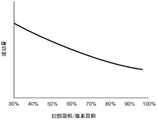
图9是表示分光特性的波动量与凹部的面积的关系的曲线图。FIG. 9 is a graph showing the relationship between the fluctuation amount of the spectral characteristics and the area of the concave portion.
具体实施方式Detailed ways
以下,参照附图对实施方式进行说明。另外,在各图中,对于相同的要素赋予相同的标号。Hereinafter, embodiments will be described with reference to the drawings. In addition, in each figure, the same code|symbol is attached|subjected to the same element.
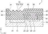
图1是第1实施方式的固体摄像装置1的示意剖视图。FIG. 1 is a schematic cross-sectional view of the solid-state imaging device 1 according to the first embodiment.
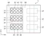
图2是第1实施方式的固体摄像装置1的示意平面图。FIG. 2 is a schematic plan view of the solid-state imaging device 1 according to the first embodiment.
图3是在图2中将绝缘膜50去除的示意平面图。FIG. 3 is a schematic plan view in which the
固体摄像装置1具有基板10、设置在基板10的表面的像素11、电荷转送晶体管20、第1布线层30、第2布线层40和绝缘膜50。The solid-state imaging device 1 includes a
设与基板10的表面平行且相互正交的两方向为X方向及Y方向。设与X方向及Y方向正交的方向为Z方向。图1是沿着图2的X方向的剖视图。Two directions parallel to the surface of the
像素11包括光电转换部。基板10例如是硅基板。像素11例如包含N型硅与P型硅的PN结。固体摄像装置1例如是线性传感器,如图3所示,多个像素11具有在Y方向上排列的像素列。The
电荷转送晶体管20具有扩散层21、栅极绝缘膜22和栅极电极23。扩散层21例如是掺杂有杂质的硅区域,在基板10的表面中设置在接近于像素11的区域中。The
在像素11与扩散层21之间的区域之上,经由栅极绝缘膜22设置有栅极电极23。Over the region between the
在基板10上的比栅极电极23靠上的层中设置有第1布线层30。第2布线层40设置在比第1布线层30靠上的层中。第1布线层30通过导通孔61与扩散层21连接。第1布线层30与电荷转送晶体管20电气地连接,与电荷转送晶体管20一起构成电路。The
第2布线层40不与电荷转送晶体管20电气地连接,主要承担遮光的功能。The
在基板10上设置有绝缘膜50,以将像素11、电荷转送晶体管20、第1布线层30及第2布线层40覆盖。此外,绝缘膜50将导通孔61的周围覆盖。An
第1布线层30及第2布线层40例如是含有铝的金属层,具有对于向像素11的入射对象的光的遮光性及反射性。The
绝缘膜50例如是硅氧化膜,具有对于向像素11的入射对象的光的透过性。The
第1布线层30在与像素11对置的区域具有第1开口31。如图3所示,沿着多个像素11的排列方向,在Y方向上排列有多个第1开口31。第1布线层30也设置于在Y方向上相邻的像素11之间。The
第1开口31的X方向的宽度比像素11的X方向的宽度小,第1开口31的边缘在像素11的上方位于与像素11重叠的区域中。The width of the
第2布线层40具有与第1布线层30的第1开口31对置的第2开口41。如图3所示,第2开口41沿着排列有多个第1开口31的区域在Y方向上以狭缝状延伸。The
第2开口41的边缘与第1开口31的边缘相比,向从第1开口31的中心远离的方向后退。第2开口41的边缘与第1开口31的边缘相比沿着X方向后退。The edge of the second opening 41 retreats in a direction away from the center of the first opening 31 than the edge of the first opening 31 . The edge of the second opening 41 retreats in the X direction than the edge of the first opening 31 .
绝缘膜50具有设置在与第2开口41对置的区域的多个凹部51。各个凹部51在俯视下具有圆形状的开口51a和有曲率的凹面51b。凹部51的开口51a的形状并不限于正圆。在图1所示的例子中,绝缘膜50的一部分以凸状设置于在X方向上相邻的凹部51之间。此外,绝缘膜50的一部分以凸状设置于在Y方向上相邻的凹部51之间。The
在1个像素11的上方区域配置有多个凹部51。多个凹部51配置在比第2开口41的边缘靠内侧的区域。凹部51的一部分与第1开口31的外侧的区域重叠。A plurality of
由第1布线层30和第2布线层40将基板10的表面的像素11以外的区域覆盖而遮光。The regions other than the
图8是表示多个凹部51的形成方法的示意平面图。FIG. 8 is a schematic plan view showing a method of forming the plurality of
在基板10上形成第1布线层30、第2布线层40、绝缘膜50等之后,在绝缘膜50上形成抗蚀剂70。After the
接着,通过对于抗蚀剂70的曝光及显影,在抗蚀剂70的位于像素11的上方的区域中形成多个开口71。以该抗蚀剂70为掩模,对绝缘膜50的表面进行湿式蚀刻。在绝缘膜50中,从在抗蚀剂70的开口71露出的部分起,如在图8中用虚线表示的那样,蚀刻各向同性地进展,形成多个凹部51。Next, by exposing and developing the resist 70 , a plurality of
没有直接向像素11入射而由基板10的表面反射而向上方返回的光能够由凹部51的有曲率的凹面51b反射。由该凹面51b反射的光通过凹透镜效果而扩散,变得难以向像素11入射。因而,能够抑制因这样的反射光与直接入射到像素11中的光的干涉造成的分光特性的波动。The light that is not directly incident on the
图9是表示分光特性的波动量与凹部51的面积的关系的曲线图。FIG. 9 is a graph showing the relationship between the amount of fluctuation in the spectral characteristics and the area of the
横轴表示多个凹部51(配置在1个像素11的上方的多个凹部51)的面积相对于1个像素11的面积的比。这里,凹部51的面积不是表示也包括凹面51b的凹部51的表面积,而是表示在俯视下配置有多个开口51a的区域的面积。The horizontal axis represents the ratio of the area of the plurality of concave portions 51 (the plurality of
根据图9的曲线图可以确认,凹部51的面积越大,波动抑制效果越大。From the graph of FIG. 9 , it can be confirmed that the larger the area of the
如果增大凹部51的面积,则担心发生凹部51与第2布线层40的交叠,而第2布线层40从绝缘膜50露出。第2布线层40的露出导致可靠性的下降。另一方面,以不与第2布线层40交叠的方式形成凹部51会阻碍凹部51的面积扩大。If the area of the
在固体摄像装置中,通常最上层的布线层承担遮光的功能。根据实施方式,不是仅由最上层的布线层(第2布线层40)承担遮光的功能,也由设置在第2布线层40之下的第1布线层30承担遮光的功能。即,用不同层的多个布线层将像素11以外的区域覆盖而遮光。In a solid-state imaging device, generally, the uppermost wiring layer has a function of shielding light. According to the embodiment, not only the uppermost wiring layer (second wiring layer 40 ) has the function of shielding light, but also the
像素11的外边缘的附近区域被第1布线层30遮光。因此,能够将第2布线层40的第2开口41的宽度(X方向的宽度)扩大为比像素11的宽度(X方向的宽度)大。相应于该第2开口41的宽度扩大,能够扩大凹部51的区域。因而,根据实施方式,能够在将最上层的第2布线层40用绝缘膜50可靠地覆盖、保护的同时,将凹部51的区域扩大而提高波动的抑制效果。The region near the outer edge of the
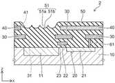
图4是第2实施方式的固体摄像装置2的示意剖视图。FIG. 4 is a schematic cross-sectional view of the solid-
图5是第2实施方式的固体摄像装置2的示意平面图。FIG. 5 is a schematic plan view of the solid-
图4是沿着图5的X方向的剖视图。FIG. 4 is a cross-sectional view taken along the X direction of FIG. 5 .
凹部51的圆形状的开口51a具有在俯视下与其他凹部51的开口51a重叠的区域。凹部51的开口51a的一部分与在X方向上相邻的其他凹部51的开口51a的一部分重叠。凹部51的开口51a的一部分与在Y方向上相邻的其他凹部51的开口51a的一部分重叠。The
如果在像素11的上方区域中的绝缘膜50上有平坦面,则由基板10的表面反射的光在该平坦面上反射而容易向像素11入射,容易引起直接入射光与反射光的干涉。根据第2实施方式,通过使多个凹部51的开口51a相互重叠,像素11的上方区域中的绝缘膜50的平坦部的面积减小,能够进一步提高波动抑制效果。If there is a flat surface on the insulating
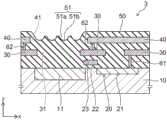
图6是第3实施方式的固体摄像装置3的示意剖视图。FIG. 6 is a schematic cross-sectional view of the solid-
图7是第3实施方式的固体摄像装置3的示意平面图。FIG. 7 is a schematic plan view of the solid-
图6是沿着图7的X方向的剖视图。FIG. 6 is a cross-sectional view taken along the X direction of FIG. 7 .
在第2开口41的边缘的附近的第2布线层40与第1布线层30之间,设置有多个导通孔62。导通孔62将第2布线层40与第1布线层30连接。导通孔62是对于向像素11的入射对象的光具有反射性的金属部件。A plurality of via
如图7所示,在像素11的X方向的边缘的附近,沿Y方向排列有多个导通孔62。以在X方向夹着像素11的上方区域的方式配置有多个导通孔62。As shown in FIG. 7 , in the vicinity of the edge in the X direction of the
能够使由凹部51的凹面51b反射而扩散的光由导通孔62反射而朝向像素11。这减少了不向像素11入射的反射光,使感度提高。The light reflected and diffused by the
说明了本发明的几个实施方式,但这些实施方式是作为例子提示的,不是要限定发明的范围。这些新的实施方式能够以其他各种各样的形态实施,在不脱离发明的主旨的范围内能够进行各种各样的省略、替换、变更。这些实施方式及其变形包含在发明的范围或主旨中,并且包含在权利要求书所记载的发明和其等价的范围中。Several embodiments of the present invention have been described, but these embodiments are presented as examples and are not intended to limit the scope of the invention. These new embodiments can be implemented in various other forms, and various omissions, substitutions, and changes can be made without departing from the gist of the invention. These embodiments and modifications thereof are included in the scope and spirit of the invention, and are included in the invention described in the claims and the scope of its equivalents.
Claims (14)
Applications Claiming Priority (2)
| Application Number | Priority Date | Filing Date | Title |
|---|---|---|---|
| JP2018152303AJP2020027887A (en) | 2018-08-13 | 2018-08-13 | Solid-state imaging apparatus |
| JP2018-152303 | 2018-08-13 |
Publications (1)
| Publication Number | Publication Date |
|---|---|
| CN110828491Atrue CN110828491A (en) | 2020-02-21 |
Family
ID=69406438
Family Applications (1)
| Application Number | Title | Priority Date | Filing Date |
|---|---|---|---|
| CN201910159688.0AWithdrawnCN110828491A (en) | 2018-08-13 | 2019-03-04 | Solid-state imaging device |
Country Status (3)
| Country | Link |
|---|---|
| US (1) | US10825852B2 (en) |
| JP (1) | JP2020027887A (en) |
| CN (1) | CN110828491A (en) |
Families Citing this family (1)
| Publication number | Priority date | Publication date | Assignee | Title |
|---|---|---|---|---|
| JP7624806B2 (en)* | 2020-04-03 | 2025-01-31 | 浜松ホトニクス株式会社 | Solid-state imaging device |
Citations (3)
| Publication number | Priority date | Publication date | Assignee | Title |
|---|---|---|---|---|
| JP2001267544A (en)* | 2000-03-21 | 2001-09-28 | Sharp Corp | Solid-state imaging device and method of manufacturing the same |
| US20110096214A1 (en)* | 2009-10-27 | 2011-04-28 | Kabushiki Kaisha Toshiba | Solid-state imaging device and method of manufacturing the same |
| US20120001292A1 (en)* | 2010-06-30 | 2012-01-05 | Kabushiki Kaisha Toshiba | Method for producing solid state imaging device and solid-state imaging device |
Family Cites Families (5)
| Publication number | Priority date | Publication date | Assignee | Title |
|---|---|---|---|---|
| KR100687102B1 (en)* | 2005-03-30 | 2007-02-26 | 삼성전자주식회사 | Image sensor and its manufacturing method. |
| JP2008177191A (en)* | 2007-01-16 | 2008-07-31 | Matsushita Electric Ind Co Ltd | Solid-state imaging device and camera using the same |
| JP5468353B2 (en)* | 2009-10-27 | 2014-04-09 | 株式会社東芝 | Solid-state image sensor |
| JP2012204686A (en) | 2011-03-25 | 2012-10-22 | Toshiba Corp | Solid state image pickup device and manufacturing method of the same |
| JP2016082133A (en) | 2014-10-20 | 2016-05-16 | ソニー株式会社 | Solid-state imaging device and electronic apparatus |
- 2018
- 2018-08-13JPJP2018152303Apatent/JP2020027887A/enactivePending
- 2019
- 2019-01-18USUS16/251,431patent/US10825852B2/enactiveActive
- 2019-03-04CNCN201910159688.0Apatent/CN110828491A/ennot_activeWithdrawn
Patent Citations (3)
| Publication number | Priority date | Publication date | Assignee | Title |
|---|---|---|---|---|
| JP2001267544A (en)* | 2000-03-21 | 2001-09-28 | Sharp Corp | Solid-state imaging device and method of manufacturing the same |
| US20110096214A1 (en)* | 2009-10-27 | 2011-04-28 | Kabushiki Kaisha Toshiba | Solid-state imaging device and method of manufacturing the same |
| US20120001292A1 (en)* | 2010-06-30 | 2012-01-05 | Kabushiki Kaisha Toshiba | Method for producing solid state imaging device and solid-state imaging device |
Also Published As
| Publication number | Publication date |
|---|---|
| JP2020027887A (en) | 2020-02-20 |
| US20200052023A1 (en) | 2020-02-13 |
| US10825852B2 (en) | 2020-11-03 |
Similar Documents
| Publication | Publication Date | Title |
|---|---|---|
| CN110137190B (en) | Photoelectric conversion apparatus and device | |
| JP5814626B2 (en) | Photoelectric conversion device and method of manufacturing photoelectric conversion device | |
| US9906743B2 (en) | Solid-state imaging apparatus and imaging system having a light shielding portion | |
| JP5513872B2 (en) | Solid-state imaging device | |
| CN109360829B (en) | Pixel array substrate | |
| US20160043123A1 (en) | Semiconductor structure and manufacturing method thereof | |
| US9837463B2 (en) | Solid-state imaging device and method of manufacturing the same | |
| US20070037406A1 (en) | Methods of fabricating a semiconductor device using a photosensitive polyimide layer and semiconductor devices fabricated thereby | |
| CN110828491A (en) | Solid-state imaging device | |
| US10431617B2 (en) | Photoelectric conversion device and apparatus | |
| JP2013182943A (en) | Method of manufacturing solid state imaging device | |
| JP2019186473A (en) | Semiconductor device and method for manufacturing the same | |
| US6809355B2 (en) | Solid-state imaging device | |
| US20170018595A1 (en) | Method of fabricating light pipe of image sensing device | |
| CN110401803B (en) | Solid-state image pickup device | |
| US11145685B2 (en) | Image capturing device and camera | |
| JP2009218374A (en) | Solid-state imaging device | |
| JP2016029704A (en) | Photoelectric conversion device and imaging system using the same | |
| CN112530983B (en) | Image sensor | |
| US20070290242A1 (en) | Solid-state imaging device having transmission gates which pass over part of photo diodes when seen from the thickness direction of the semiconductor substrate | |
| JP2012204686A (en) | Solid state image pickup device and manufacturing method of the same | |
| JP6268781B2 (en) | Semiconductor device and manufacturing method of semiconductor device | |
| JP2014041928A (en) | Semiconductor device | |
| JP2015060931A (en) | Photodetector and sensor package | |
| JP2012084687A (en) | Semiconductor device |
Legal Events
| Date | Code | Title | Description |
|---|---|---|---|
| PB01 | Publication | ||
| PB01 | Publication | ||
| SE01 | Entry into force of request for substantive examination | ||
| SE01 | Entry into force of request for substantive examination | ||
| WW01 | Invention patent application withdrawn after publication | Application publication date:20200221 | |
| WW01 | Invention patent application withdrawn after publication |