CN110828364B - Mass transfer method, manufacturing method of display device, and display device - Google Patents
Mass transfer method, manufacturing method of display device, and display deviceDownload PDFInfo
- Publication number
- CN110828364B CN110828364BCN201911141924.2ACN201911141924ACN110828364BCN 110828364 BCN110828364 BCN 110828364BCN 201911141924 ACN201911141924 ACN 201911141924ACN 110828364 BCN110828364 BCN 110828364B
- Authority
- CN
- China
- Prior art keywords
- micro
- substrate
- temporary substrate
- led array
- emitting diode
- Prior art date
- Legal status (The legal status is an assumption and is not a legal conclusion. Google has not performed a legal analysis and makes no representation as to the accuracy of the status listed.)
- Active
Links
- 238000012546transferMethods0.000titleclaimsabstractdescription71
- 238000000034methodMethods0.000titleclaimsabstractdescription65
- 238000004519manufacturing processMethods0.000titleclaimsabstractdescription15
- 239000000758substrateSubstances0.000claimsabstractdescription178
- 238000001039wet etchingMethods0.000claimsabstractdescription17
- 239000004065semiconductorSubstances0.000claimsabstractdescription13
- 239000012790adhesive layerSubstances0.000claimsdescription64
- 239000000463materialSubstances0.000claimsdescription15
- 239000000853adhesiveSubstances0.000claimsdescription10
- 230000001070adhesive effectEffects0.000claimsdescription10
- 238000010438heat treatmentMethods0.000claimsdescription9
- 238000000926separation methodMethods0.000claimsdescription5
- 230000000007visual effectEffects0.000claimsdescription2
- 230000005855radiationEffects0.000claims2
- 238000005260corrosionMethods0.000abstractdescription9
- 238000006073displacement reactionMethods0.000abstractdescription8
- 230000007797corrosionEffects0.000abstractdescription7
- 238000005530etchingMethods0.000description20
- 239000010410layerSubstances0.000description16
- 238000010586diagramMethods0.000description15
- 238000005516engineering processMethods0.000description11
- 230000001678irradiating effectEffects0.000description5
- 238000003491arrayMethods0.000description4
- 238000001312dry etchingMethods0.000description3
- 229920002120photoresistant polymerPolymers0.000description3
- 229910002704AlGaNInorganic materials0.000description2
- 229910002601GaNInorganic materials0.000description2
- 229910005540GaPInorganic materials0.000description2
- 229910001218Gallium arsenideInorganic materials0.000description2
- 230000000295complement effectEffects0.000description2
- 238000007689inspectionMethods0.000description2
- 239000004973liquid crystal related substanceSubstances0.000description2
- 229910044991metal oxideInorganic materials0.000description2
- 150000004706metal oxidesChemical class0.000description2
- 238000012986modificationMethods0.000description2
- 230000004048modificationEffects0.000description2
- 229910003465moissaniteInorganic materials0.000description2
- 230000035945sensitivityEffects0.000description2
- 229910010271silicon carbideInorganic materials0.000description2
- 239000010409thin filmSubstances0.000description2
- 238000006243chemical reactionMethods0.000description1
- 238000011161developmentMethods0.000description1
- 239000003292glueSubstances0.000description1
- 238000009776industrial productionMethods0.000description1
- 239000007788liquidSubstances0.000description1
- 238000002360preparation methodMethods0.000description1
- 238000012545processingMethods0.000description1
- 229910000679solderInorganic materials0.000description1
- 239000011345viscous materialSubstances0.000description1
Images


Classifications
- H—ELECTRICITY
- H01—ELECTRIC ELEMENTS
- H01L—SEMICONDUCTOR DEVICES NOT COVERED BY CLASS H10
- H01L21/00—Processes or apparatus adapted for the manufacture or treatment of semiconductor or solid state devices or of parts thereof
- H01L21/67—Apparatus specially adapted for handling semiconductor or electric solid state devices during manufacture or treatment thereof; Apparatus specially adapted for handling wafers during manufacture or treatment of semiconductor or electric solid state devices or components ; Apparatus not specifically provided for elsewhere
- H01L21/683—Apparatus specially adapted for handling semiconductor or electric solid state devices during manufacture or treatment thereof; Apparatus specially adapted for handling wafers during manufacture or treatment of semiconductor or electric solid state devices or components ; Apparatus not specifically provided for elsewhere for supporting or gripping
- H01L21/6835—Apparatus specially adapted for handling semiconductor or electric solid state devices during manufacture or treatment thereof; Apparatus specially adapted for handling wafers during manufacture or treatment of semiconductor or electric solid state devices or components ; Apparatus not specifically provided for elsewhere for supporting or gripping using temporarily an auxiliary support
- G—PHYSICS
- G09—EDUCATION; CRYPTOGRAPHY; DISPLAY; ADVERTISING; SEALS
- G09F—DISPLAYING; ADVERTISING; SIGNS; LABELS OR NAME-PLATES; SEALS
- G09F9/00—Indicating arrangements for variable information in which the information is built-up on a support by selection or combination of individual elements
- G09F9/30—Indicating arrangements for variable information in which the information is built-up on a support by selection or combination of individual elements in which the desired character or characters are formed by combining individual elements
- G09F9/33—Indicating arrangements for variable information in which the information is built-up on a support by selection or combination of individual elements in which the desired character or characters are formed by combining individual elements being semiconductor devices, e.g. diodes
- H—ELECTRICITY
- H10—SEMICONDUCTOR DEVICES; ELECTRIC SOLID-STATE DEVICES NOT OTHERWISE PROVIDED FOR
- H10H—INORGANIC LIGHT-EMITTING SEMICONDUCTOR DEVICES HAVING POTENTIAL BARRIERS
- H10H29/00—Integrated devices, or assemblies of multiple devices, comprising at least one light-emitting semiconductor element covered by group H10H20/00
- H10H29/10—Integrated devices comprising at least one light-emitting semiconductor component covered by group H10H20/00
- H10H29/14—Integrated devices comprising at least one light-emitting semiconductor component covered by group H10H20/00 comprising multiple light-emitting semiconductor components
- H—ELECTRICITY
- H01—ELECTRIC ELEMENTS
- H01L—SEMICONDUCTOR DEVICES NOT COVERED BY CLASS H10
- H01L2221/00—Processes or apparatus adapted for the manufacture or treatment of semiconductor or solid state devices or of parts thereof covered by H01L21/00
- H01L2221/67—Apparatus for handling semiconductor or electric solid state devices during manufacture or treatment thereof; Apparatus for handling wafers during manufacture or treatment of semiconductor or electric solid state devices or components; Apparatus not specifically provided for elsewhere
- H01L2221/683—Apparatus for handling semiconductor or electric solid state devices during manufacture or treatment thereof; Apparatus for handling wafers during manufacture or treatment of semiconductor or electric solid state devices or components; Apparatus not specifically provided for elsewhere for supporting or gripping
- H01L2221/68304—Apparatus for handling semiconductor or electric solid state devices during manufacture or treatment thereof; Apparatus for handling wafers during manufacture or treatment of semiconductor or electric solid state devices or components; Apparatus not specifically provided for elsewhere for supporting or gripping using temporarily an auxiliary support
- H01L2221/68381—Details of chemical or physical process used for separating the auxiliary support from a device or wafer
- H01L2221/68386—Separation by peeling
Landscapes
- Engineering & Computer Science (AREA)
- Physics & Mathematics (AREA)
- General Physics & Mathematics (AREA)
- Theoretical Computer Science (AREA)
- Condensed Matter Physics & Semiconductors (AREA)
- Manufacturing & Machinery (AREA)
- Computer Hardware Design (AREA)
- Microelectronics & Electronic Packaging (AREA)
- Power Engineering (AREA)
- Led Device Packages (AREA)
Abstract
Description
Translated fromChinese技术领域technical field
本申请涉及半导体器件制造技术领域,具体而言,涉及一种巨量转移方法、显示装置的制作方法和显示装置。The present application relates to the technical field of semiconductor device manufacturing, in particular, to a mass transfer method, a manufacturing method of a display device, and a display device.
背景技术Background technique
微型发光二极管(Micro-LED)就是“微”LED(发光二极管),微型发光二极管阵列显示作为一种新显示技术,与其它显示技术,比如液晶显示(Liquid Crystal Display,LCD)、有机电激光显示(OrganicLight-Emitting Diode,OLED)等离子显示(Plasma DisplayPanel,PDP)等相比,其核心的不同之处在于其采用无机LED作为发光像素。Micro-LED (Micro-LED) is "micro" LED (light-emitting diode). Micro-LED array display is a new display technology, and other display technologies, such as liquid crystal display (Liquid Crystal Display, LCD), organic electromechanical laser display (OrganicLight-Emitting Diode, OLED) Plasma Display (Plasma DisplayPanel, PDP), etc., the core difference is that it uses inorganic LEDs as light-emitting pixels.
制作好的微小的LED需要转移到做好驱动电路的基底上。无论是电视还是手机屏,其像素的数量都是相当巨大的,而像素的尺寸较小,并且显示产品对于像素错误的容忍度也很低,一块有“亮点”或“暗点”的显示屏无法满足用户需求,所以将这些小像素可靠地转移到做好驱动电路的衬底上并实现电路连接是十分困难、复杂的技术。实际上,“巨量转移”确实是目前Micro-LED商业化上面的一大瓶颈技术。其转移的效率,成功率都决定着商业化的成功与否。如何提高巨量转移后Micro-LED器件的良品率是值得研究的问题。The tiny LEDs that have been fabricated need to be transferred to the substrate on which the driving circuit is prepared. Whether it is a TV or a mobile phone screen, the number of pixels is quite large, and the size of the pixels is small, and the display product has a low tolerance for pixel errors. A display with "bright spots" or "dark spots" It cannot meet the needs of users, so it is very difficult and complicated technology to reliably transfer these small pixels to the substrate of the driver circuit and realize the circuit connection. In fact, "mass transfer" is indeed a major bottleneck technology in the commercialization of Micro-LED. The efficiency and success rate of its transfer determine the success of commercialization. How to improve the yield rate of Micro-LED devices after mass transfer is a problem worth studying.
发明内容Contents of the invention
有鉴于此,本申请的目的在于提供一种巨量转移方法、显示装置的制作方法和显示装置,以解决上述问题。In view of this, the object of the present application is to provide a mass transfer method, a manufacturing method of a display device and a display device, so as to solve the above problems.
本申请提供一种技术方案:The application provides a technical solution:
第一方面,实施例提供一种巨量转移方法,包括:In the first aspect, the embodiment provides a mass transfer method, including:
对制备有微型发光二极管阵列的原始基底进行湿法腐蚀,以使所述微型发光二极管阵列与所述原始基底的接触面积减小;performing wet etching on the original substrate prepared with the array of micro light emitting diodes, so that the contact area between the array of micro light emitting diodes and the original substrate is reduced;
将所述微型发光二极管阵列远离所述原始基底的一侧与第一临时衬底结合;combining the side of the miniature LED array away from the original substrate with a first temporary substrate;
再次对所述原始基底进行湿法腐蚀,以使所述微型发光二极管阵列与所述原始基底剥离,去除所述原始基底;performing wet etching on the original substrate again, so that the micro light emitting diode array is peeled off from the original substrate, and the original substrate is removed;
通过所述第一临时衬底,将所述微型发光二极管阵列与目标基板结合,完成巨量转移。Through the first temporary substrate, the micro light emitting diode array is combined with the target substrate to complete mass transfer.
在可选的实施方式中,所述通过所述第一临时衬底,将所述微型发光二极管阵列与目标基板结合的步骤包括:In an optional embodiment, the step of combining the micro-LED array with the target substrate through the first temporary substrate includes:
将位于所述第一临时衬底的微型发光二极管阵列远离所述第一临时衬底的一侧与第二临时衬底结合,并分离所述第一临时衬底与所述微型发光二极管阵列;combining the micro light emitting diode array located on the first temporary substrate away from the first temporary substrate with a second temporary substrate, and separating the first temporary substrate from the micro light emitting diode array;
将位于所述第二临时衬底的微型发光二极管阵列远离所述第二临时衬底的一侧与目标基板结合。Combining the side of the micro light emitting diode array located on the second temporary substrate away from the second temporary substrate with the target substrate.
在可选的实施方式中,所述微型发光二极管阵列通过第一粘合层与所述第一临时衬底结合,所述分离所述第一临时衬底与所述微型发光二极管阵列的步骤包括:In an optional embodiment, the micro-LED array is combined with the first temporary substrate through a first adhesive layer, and the step of separating the first temporary substrate from the micro-LED array includes :
加热所述第一粘合层,降低所述第一粘合层与所述微型发光二极管阵列相接触的区域的粘附力,从而分离所述第一临时衬底与所述微型发光二极管阵列。The first adhesive layer is heated to reduce the adhesive force of the area where the first adhesive layer is in contact with the micro-LED array, thereby separating the first temporary substrate from the micro-LED array.
在可选的实施方式中,所述微型发光二极管阵列通过第一粘合层与所述第一临时衬底结合,所述分离所述第一临时衬底与所述微型发光二极管阵列的步骤包括:In an optional embodiment, the micro-LED array is combined with the first temporary substrate through a first adhesive layer, and the step of separating the first temporary substrate from the micro-LED array includes :
使用紫外线照射所述第一粘合层,降低所述第一粘合层与所述微型发光二极管阵列相接触的区域的粘附力,以分离所述第一临时衬底与所述微型发光二极管阵列。Using ultraviolet rays to irradiate the first adhesive layer to reduce the adhesive force of the area where the first adhesive layer is in contact with the micro-LED array, so as to separate the first temporary substrate from the micro-LEDs array.
在可选的实施方式中,所述第一粘合层为光刻胶层。In an optional embodiment, the first adhesive layer is a photoresist layer.
在可选的实施方式中,所述微型发光二极管阵列通过第二粘合层与所述第二临时衬底结合。In an optional embodiment, the micro light emitting diode array is combined with the second temporary substrate through a second adhesive layer.
在可选的实施方式中,所述第二粘合层为粘合胶层。In an optional embodiment, the second adhesive layer is an adhesive glue layer.
在可选的实施方式中,所述原始基底采用半导体材料制成。In an optional implementation manner, the original substrate is made of semiconductor material.
第二方面,实施例提供一种显示装置的制作方法,采用前述实施方式任意一项所述的巨量转移方法实现微型发光二极管阵列的巨量转移。In a second aspect, the embodiment provides a method for manufacturing a display device, using the mass transfer method described in any one of the foregoing embodiments to realize mass transfer of micro-LED arrays.
第三方面,实施例提供一种显示装置,采用前述实施方式所述的显示装置制作方法制作形成。In a third aspect, the embodiment provides a display device, which is manufactured by using the method for manufacturing the display device described in the foregoing embodiments.
本申请实施例提供了一种巨量转移方法、显示装置的制作方法和显示装置,该巨量转移方法通过先对原始基底进行部分腐蚀,然后将微型发光二极管阵列与临时衬底粘合,继续腐蚀原始基底,直至腐蚀完全。最后通过临时衬底将阵列放置于目标基板,完成巨量转移,如此,通过采用临时衬底固定微型发光二极管阵列与逐次腐蚀相结合的方式减少了微型发光二极管阵列巨量转移过程中发生丢失的概率,减小了位移误差,从而提升了良品率。The embodiment of the present application provides a mass transfer method, a manufacturing method of a display device, and a display device. The mass transfer method first partially etches the original substrate, and then bonds the micro light-emitting diode array to the temporary substrate. Etch the original substrate until the corrosion is complete. Finally, the array is placed on the target substrate through the temporary substrate to complete the mass transfer. In this way, the combination of using the temporary substrate to fix the micro-LED array and sequential etching reduces the loss of the micro-LED array during the mass transfer process. Probability, reducing the displacement error, thereby improving the yield.
附图说明Description of drawings
为了更清楚地说明本申请实施例的技术方案,下面将对实施例中所需要使用的附图作简单地介绍,应当理解,以下附图仅示出了本申请的某些实施例,因此不应被看作是对范围的限定,对于本领域普通技术人员来讲,在不付出创造性劳动的前提下,还可以根据这些附图获得其他相关的附图。In order to more clearly illustrate the technical solutions of the embodiments of the present application, the accompanying drawings that are required in the embodiments will be briefly introduced below. It should be understood that the following drawings only show some embodiments of the present application, and thus It should be regarded as a limitation on the scope, and those skilled in the art can also obtain other related drawings based on these drawings without creative work.
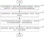
图1为本申请实施例提供的巨量转移方法的流程图。FIG. 1 is a flowchart of a mass transfer method provided by an embodiment of the present application.
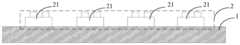
图2为本申请实施例提供的制备有微型发光二极管阵列的原始基底的结构示意图。FIG. 2 is a schematic structural view of an original substrate prepared with a micro-LED array provided in an embodiment of the present application.
图3为本申请实施例提供的巨量转移方法的步骤S1对应的示意图。FIG. 3 is a schematic diagram corresponding to step S1 of the bulk transfer method provided by the embodiment of the present application.
图4为本申请实施例提供的巨量转移方法的步骤S2对应的示意图。FIG. 4 is a schematic diagram corresponding to step S2 of the mass transfer method provided by the embodiment of the present application.
图5为本申请实施例提供的巨量转移方法的步骤S3对应的示意图。FIG. 5 is a schematic diagram corresponding to step S3 of the mass transfer method provided by the embodiment of the present application.
图6为本申请实施例提供的步骤S4的子步骤流程图。FIG. 6 is a flow chart of sub-steps of step S4 provided by the embodiment of the present application.
图7为本申请实施例提供的巨量转移方法的步骤S41对应的示意图之一。FIG. 7 is one of the schematic diagrams corresponding to step S41 of the mass transfer method provided by the embodiment of the present application.
图8为本申请实施例提供的巨量转移方法的步骤S41对应的示意图之二。FIG. 8 is the second schematic diagram corresponding to step S41 of the mass transfer method provided by the embodiment of the present application.
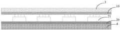
图9为本申请实施例提供的巨量转移方法的步骤S42对应的示意图。FIG. 9 is a schematic diagram corresponding to step S42 of the mass transfer method provided by the embodiment of the present application.
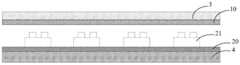
图10为本申请实施例提供的一种显示装置的示意图。FIG. 10 is a schematic diagram of a display device provided by an embodiment of the present application.
图标:1-原始基底;2-微型发光二极管阵列;21-微型发光二极管;3-第一临时衬底;4-第二临时衬底;5-目标基板;10-第一粘合层;20-第二粘合层;100-显示装置;110-显示面板。Icons: 1-original substrate; 2-micro-LED array; 21-micro-LED; 3-first temporary substrate; 4-second temporary substrate; 5-target substrate; 10-first adhesive layer; 20 - second adhesive layer; 100 - display device; 110 - display panel.
具体实施方式Detailed ways
为使本申请实施例的目的、技术方案和优点更加清楚,下面将结合本申请实施例中的附图,对本申请实施例中的技术方案进行清楚、完整地描述,显然,所描述的实施例是本申请一部分实施例,而不是全部的实施例。通常在此处附图中描述和示出的本申请实施例的组件可以以各种不同的配置来布置和设计。In order to make the purposes, technical solutions and advantages of the embodiments of the present application clearer, the technical solutions in the embodiments of the present application will be clearly and completely described below in conjunction with the drawings in the embodiments of the present application. Obviously, the described embodiments It is a part of the embodiments of this application, not all of them. The components of the embodiments of the application generally described and illustrated in the figures herein may be arranged and designed in a variety of different configurations.
因此,以下对在附图中提供的本申请的实施例的详细描述并非旨在限制要求保护的本申请的范围,而是仅仅表示本申请的选定实施例。基于本申请中的实施例,本领域普通技术人员在没有作出创造性劳动前提下所获得的所有其他实施例,都属于本申请保护的范围。Accordingly, the following detailed description of the embodiments of the application provided in the accompanying drawings is not intended to limit the scope of the claimed application, but merely represents selected embodiments of the application. Based on the embodiments in this application, all other embodiments obtained by persons of ordinary skill in the art without creative efforts fall within the protection scope of this application.
在本申请的描述中,还需要说明的是,除非另有明确的规定和限定,术语“设置”、“连接”以及“结合”应做广义理解,例如,可以是固定连接,也可以是可拆卸连接,或一体地连接。可以是机械连接,也可以是电连接。可以是直接相连,也可以通过中间媒介间接相连,可以是两个元件内部的连通。对于本领域的普通技术人员而言,可以具体情况理解上述术语在本申请中的具体含义。In the description of this application, it should also be noted that, unless otherwise clearly specified and limited, the terms "arrangement", "connection" and "combination" should be interpreted in a broad sense, for example, it can be a fixed connection or a flexible connection. Disassemble the connection, or connect in one piece. It can be a mechanical connection or an electrical connection. It can be directly connected, or indirectly connected through an intermediary, and can be internally connected between two components. Those of ordinary skill in the art can understand the specific meanings of the above terms in this application in specific situations.
应注意到:相似的标号和字母在下面的附图中表示类似项,因此,一旦某一项在一个附图中被定义,则在随后的附图中不需要对其进行进一步定义和解释。It should be noted that like numerals and letters denote similar items in the following figures, therefore, once an item is defined in one figure, it does not require further definition and explanation in subsequent figures.
在本申请的描述中,需要理解的是,术语“中心”、“上”、“下”、“左”、“右”、“竖直”、“水平”、“内”、“外”等指示的方位或位置关系为基于附图所示的方位或位置关系,或者是该申请产品使用时惯常摆放的方位或位置关系,或者是本领域技术人员惯常理解的方位或位置关系,仅是为了便于描述本申请和简化描述,而不是指示或暗示所指的设备或元件必须具有特定的方位、以特定的方位构造和操作,因此不能理解为对本申请的限制。In the description of this application, it is to be understood that the terms "center", "upper", "lower", "left", "right", "vertical", "horizontal", "inner", "outer", etc. The indicated orientation or positional relationship is based on the orientation or positional relationship shown in the drawings, or the orientation or positional relationship that is usually placed when the application product is used, or the orientation or positional relationship that is commonly understood by those skilled in the art. In order to facilitate the description of the present application and simplify the description, it does not indicate or imply that the referred device or element must have a specific orientation, be constructed and operated in a specific orientation, and thus should not be construed as limiting the present application.
此外,术语“第一”、“第二”、“第三”等仅用于区分描述,而不能理解为指示或暗示相对重要性。In addition, the terms "first", "second", "third", etc. are only used for distinguishing descriptions, and should not be construed as indicating or implying relative importance.
Micro-LED具有轻薄、长寿命、低功耗、低成本的优势,在显示领域有极广阔的应用前景,是产业界共同追求的目标。全彩色Micro-LED技术为其领域发展的必然趋势,但由于其微缩制备技术、巨量转移技术、RGB(RGB color mode)彩色化技术等问题尚未解决而进展较慢。尤其是巨量转移技术,目前还面临着如何将大量的Micro-LED器件精确转移至接收基板,同时保持Micro-LED器件较低的损失率的问题。Micro-LED has the advantages of thinness, long life, low power consumption, and low cost. It has a very broad application prospect in the display field and is a common goal pursued by the industry. Full-color Micro-LED technology is an inevitable trend in the development of its field, but progress is slow due to unresolved issues such as its micro-scale preparation technology, mass transfer technology, and RGB (RGB color mode) colorization technology. In particular, mass transfer technology is currently facing the problem of how to accurately transfer a large number of Micro-LED devices to the receiving substrate while maintaining a low loss rate of Micro-LED devices.
如背景技术部分所介绍,目前的巨量转移技术一般先将微型发光二极管阵列与临时衬底粘合,然后再对原始基底进行腐蚀。由于腐蚀速率的均匀性难以控制,会造成部分芯片在掏空过程中过腐蚀而丢失,良率有限。如何提高巨量转移后显示装置的良品率是值得研究的问题。As introduced in the background technology section, in the current mass transfer technology, the micro light-emitting diode array is generally bonded to a temporary substrate first, and then the original substrate is etched. Because the uniformity of the etching rate is difficult to control, some chips will be lost due to over-etching during the hollowing process, and the yield rate is limited. How to improve the yield rate of the display device after mass transfer is a problem worth studying.
有鉴于此,本申请实施例提供了一种巨量转移方法,该方法通过先对原始基底进行部分腐蚀,留出空间便于腐蚀液补给。然后将微型发光二极管阵列与临时衬底粘合,继续腐蚀原始基底,直至腐蚀完全。最后通过临时衬底将微型发光二极管阵列放置于目标基板,完成巨量转移,从而减少微型发光二极管阵列巨量转移过程中发生丢失的概率,减小位移误差,提升良品率。下面对上述方法进行详细阐述。In view of this, the embodiment of the present application provides a mass transfer method. In this method, the original substrate is partially etched first, leaving a space for the replenishment of the etching solution. Then bond the micro-LED array to the temporary substrate, and continue to etch the original substrate until the etching is complete. Finally, the micro-LED array is placed on the target substrate through the temporary substrate to complete the mass transfer, thereby reducing the probability of loss of the micro-LED array during the mass transfer process, reducing displacement errors, and improving the yield rate. The above method will be described in detail below.
请结合参图1与图2,图1为本实施例提供的巨量转移方法的流程图,图2为本申请实施例提供的制备有微型发光二极管阵列2的原始基底1的结构示意图。本实施例提供的巨量转移方法包括如下步骤:Please refer to FIG. 1 and FIG. 2 in conjunction. FIG. 1 is a flow chart of the mass transfer method provided in this embodiment, and FIG. 2 is a schematic structural diagram of an
步骤S1,对制备有微型发光二极管阵列2的原始基底1进行湿法腐蚀,以使所述微型发光二极管阵列2与所述原始基底1的接触面积减小。Step S1 , performing wet etching on the
该原始基底1用于初步固定微型发光二极管阵列2。所述微型发光二极管阵列2包括多个依次排列的微型发光二极管21。可以理解,图2中微型发光二极管21的个数仅仅作为示意,实际工艺中微型发光二极管21的个数可以是任意个。可选地,所述原始基底1采用半导体材料制成,进一步地,该原始基底1的材质为可在原始基底1上生长微型发光二极管21外延层的半导体材料,例如,Si、GaAs、GaP、GaN、SiC、AlGaN等,在此不做限定。The
本申请实施例中,微型发光二极管21的结构可以为多种,例如,可以是同侧电极结构,即P型电极和N型电极位于衬底的同一侧。又例如,也可以是垂直电极结构,即P型电极和N型电极位于衬底的不同侧。本申请实施例对此不作限制。In the embodiment of the present application, the micro
为方便说明,本申请实施例以微型发光二极管21为同侧电极结构为例进行说明,如图2所示,原始基底1上制作有包括多个微型发光二极管21的微型发光二极管阵列2,各微型发光二极管21包括衬底以及两个电极,衬底的一侧与原始基底1连接。本申请实施例中,微型发光二极管阵列2的材质可以是GaAs、GaP、GaN、SiC、AlGaN等,微型发光二极管阵列2的材质还可以是其他半导体材料,本申请实施例中对此不作限定。For the convenience of description, the embodiment of the present application takes micro-LEDs 21 as an example to illustrate the electrode structure on the same side. As shown in FIG. The micro
本申请实施例中,微型发光二极管21还可以包括外延层,需要说明的是,本申请实施例不限定微型发光二极管21其外延层的具体结构,在一种实现方式中,微型发光二极管21的外延层可以包括N型半导体、P型半导体以及位于所述N型半导体和P型半导体之间的有源层,所述有源层可以包括多量子阱层,还可以包括其他结构。In the embodiment of the present application, the micro
请结合参阅图3,图3为本申请实施例提供的巨量转移方法的步骤S1对应的示意图。采用步骤S1中的方式对原始基底1进行湿法腐蚀,使得微型发光二极管阵列2与所述原始基底1的接触面积减小。微型发光二极管阵列2处于半悬空状态,留出空间便于腐蚀液补给。Please refer to FIG. 3 in conjunction with FIG. 3 , which is a schematic diagram corresponding to step S1 of the mass transfer method provided by the embodiment of the present application. The
目前,通常用到的原始基底1剥离的方法有激光剥离法,直接湿法刻蚀牺牲层法或直接湿法背面刻蚀衬底法。其中,激光剥离法容易对微型发光二极管阵列2造成损伤,导致剥离良率低。直接湿法刻蚀牺牲层法或直接湿法背面刻蚀衬底法,由于反应速率的控制精度差,也会造成剥离良率的损失。因此,本申请实施例逐次采用湿法腐蚀的方法控制腐蚀速率,可提高剥离良率。Currently, commonly used methods for stripping the
进一步地,鉴于采用干法刻蚀等会存在原始基底1残留,而原始基底1残留会影响后续转移的精确性,不平整的微型发光二极管阵列2在后续的转移过程中容易出现位移,使得良品率较低。本申请实施例中采用湿法腐蚀减小微型发光二极管阵列2与原始基底1的接触面积,采用湿法腐蚀后,微型发光二极管阵列2的表面较为干净,无原始基底1残留,无需再次去除残留的问题,从而能够便捷、可靠地确保良品率,相对于采用干法刻蚀等也更具备优越性。Further, in view of the fact that the
另外,干法刻蚀容易受到设备限制,难以实现大面积均匀地刻蚀,成本也较高,而湿法腐蚀的设备简单,成本低廉,腐蚀完成时间可控制在几分钟到几十分钟,也更适用于大面积的工业生产。In addition, dry etching is easy to be limited by equipment, it is difficult to achieve large-area uniform etching, and the cost is high, while wet etching has simple equipment and low cost, and the etching completion time can be controlled within a few minutes to tens of minutes, and it is also relatively expensive. It is more suitable for large-scale industrial production.
步骤S2,将所述微型发光二极管阵列2远离所述原始基底1的一侧与第一临时衬底3结合。Step S2 , combining the side of the miniature LED array 2 away from the
请结合参阅图4,图4为本申请实施例提供的巨量转移方法的步骤S2对应的示意图。Please refer to FIG. 4 in conjunction with FIG. 4 , which is a schematic diagram corresponding to step S2 of the mass transfer method provided by the embodiment of the present application.
其中,第一临时衬底3用于临时固定微型发光二极管阵列2。在一种实现方式中,可以采用第一粘合层10将微型发光二极管阵列2与原始基底1结合,避免各所述微型发光二极管21在后续处理中出现位移的情况,第一临时衬底3的材质可以灵活选择,本申请实施例中不进行限定,只要能够起到临时固定作用,并且对第一粘合层10的粘性控制无影响即可。Wherein, the first
进一步地,还可通过控制腐蚀液的浓度及补给量控制腐蚀速率,进一步减缓微型发光二极管阵列2在腐蚀的过程中因过腐蚀而丢失。其中,腐蚀液的选择、浓度及补给量可参考现有技术,根据实际情况选择,以达到控制腐蚀速率的目的,在此不做赘述。Furthermore, the corrosion rate can also be controlled by controlling the concentration and replenishment of the corrosion solution, so as to further slow down the loss of the micro LED array 2 due to over-corrosion during the corrosion process. Among them, the selection, concentration and replenishment amount of the corrosive solution can be selected according to the actual situation with reference to the prior art, so as to achieve the purpose of controlling the corrosion rate, and will not be repeated here.
同时,由于采用湿法腐蚀,其腐蚀速率较难控制,因此,本申请实施例中使用第一临时衬底3与微型发光二极管阵列2结合,如此,减缓了部分微型发光二极管阵列2在腐蚀的过程中因过腐蚀而丢失的问题。步骤S3,再次对所述原始基底1进行湿法腐蚀,以使所述微型发光二极管阵列2与所述原始基底1剥离,去除所述原始基底1。At the same time, due to the use of wet etching, the etching rate is difficult to control. Therefore, in the embodiment of the present application, the first
请结合参阅图5,图5为本申请实施例提供的巨量转移方法的步骤S3对应的示意图。将微型发光二极管阵列2临时固定于第一临时衬底3后,再次对处于半悬空状态的原始基底1进行湿法腐蚀,由于前一次腐蚀中预留有被腐蚀后形成的空间,更利于控制腐蚀效率,采用合适的腐蚀效率将原始基底1与微型发光二极管阵列2完全剥离,去除原始基底1。图5中示出的是原始基底1与微型发光二极管阵列2完全剥离后的示意图。Please refer to FIG. 5 in conjunction with FIG. 5 , which is a schematic diagram corresponding to step S3 of the mass transfer method provided by the embodiment of the present application. After the micro-LED array 2 is temporarily fixed on the first
本申请实施例中采用逐次腐蚀原始基底1的方式,以控制腐蚀速率,进而达到了避免部分微型发光二极管阵列2在腐蚀的过程中因过腐蚀而丢失的目的。In the embodiment of the present application, the method of etching the
步骤S4,通过所述第一临时衬底3,将所述微型发光二极管阵列2与目标基板5结合,完成巨量转移。Step S4, combining the micro-LED array 2 with the
在一种实现方式中,目标基板5上设置有多个驱动电极,多个所述驱动电极的排列方式可以与微型发光二极管21的排列方式相对应。该目标基板5可以为CMOS(Complementary Metal Oxide Semiconductor,互补金属氧化物半导体控制板)或TFT(Thin Film Transistor,薄膜晶体管)控制板,可以采用主动驱动或被动驱动的方式驱动所述微型发光二极管阵列2工作。In an implementation manner, multiple driving electrodes are disposed on the
由于本申请实施例中微型发光二极管阵列2需要与目标基板5上的驱动电极进行焊接,才能正常使用,在第一次转移时,微型发光二极管阵列2的电极与第一临时衬底3结合,无法直接与目标基板5中的电极进行焊接。因此,还需要通过其他临时衬底再次将微型发光二极管阵列2转移至目标基板5。请结合参阅图6,图6为本申请实施例提供的步骤S4的子步骤流程图。可通过步骤S41和步骤S42实现巨量转移。Since the micro-LED array 2 in the embodiment of the present application needs to be welded to the driving electrodes on the
步骤S41,将位于所述第一临时衬底3的微型发光二极管阵列2远离所述第一临时衬底3的一侧与第二临时衬底4结合,并分离所述第一临时衬底3与所述微型发光二极管阵列2。Step S41, combining the micro LED array 2 located on the first
请结合参阅图7与图8,图7与图8均为本申请实施例提供的巨量转移方法的步骤S41对应的示意图。如图7中所示,将位于所述第一临时衬底3的微型发光二极管阵列2远离所述第一临时衬底3的一侧,即,微型发光二极管21的衬底与第二临时衬底4通过第二粘合层20结合。接着,将第一临时衬底3与微型发光二极管阵列2分离,进而,得到如图8中所示的结构。Please refer to FIG. 7 and FIG. 8 in conjunction. FIG. 7 and FIG. 8 are schematic diagrams corresponding to step S41 of the mass transfer method provided by the embodiment of the present application. As shown in FIG. 7 , place the micro light emitting diode array 2 on the first
其中,所述第二临时衬底4为透明、耐高温、受热不变形的材质,以便于后续与微型发光二极管阵列2结合,并保证在后续剥离第一临时衬底3时,第二临时衬底4不受影响。Wherein, the second
S42,将位于所述第二临时衬底4的微型发光二极管阵列2远离所述第二临时衬底4的一侧与目标基板5结合。如此,完成了微型发光二极管阵列2的巨量转移。S42 , combining the side of the micro light emitting diode array 2 on the second
请结合参阅图9,图9为本申请实施例提供的巨量转移方法的步骤S42对应的示意图。第一临时衬底3与微型发光二极管阵列2分离后,将位于所述第二临时衬底4的微型发光二极管阵列2远离所述第二临时衬底4的一侧与目标基板5结合,即,将微型发光二极管21的电极与目标基板5中的电极对应结合,完成巨量转移。如此,使得目标基板5能够驱动微型发光二极管21工作。Please refer to FIG. 9 in conjunction with FIG. 9 , which is a schematic diagram corresponding to step S42 of the mass transfer method provided by the embodiment of the present application. After the first
本申请实施例中,所述微型发光二极管阵列2可以通过第一粘合层10与所述第一临时衬底3结合。上述第一粘合层10可以是具有适当粘性并且可以在腐蚀液中保持稳定,能够通过加热的方式或通过特定波长的光(紫外线)照射的方式减弱其粘性,以便于后续转移操作的胶层,例如,可以是光刻胶层、热剥离胶层或UV(Ultra-Violet Ray,紫外线)减粘胶层。In the embodiment of the present application, the micro LED array 2 can be combined with the first
进一步地,本申请实施例中不限定微型发光二极管阵列2与第二临时衬底4结合方式,可选地,所述微型发光二极管阵列2可以通过第二粘合层20与所述第二临时衬底4结合。Further, the embodiment of the present application does not limit the combination method of the micro light emitting diode array 2 and the second
需要说明的是,第二粘合层20具备比采取分离手段减弱粘性后的第一粘合层10的粘性更强的粘性。所述第二粘合层20同样可以为能通过加热的方式或通过特定波长的光(紫外线)照射的方式减弱粘性的胶层,例如,可以是光刻胶层、热剥离胶层或UV减粘胶层。It should be noted that the second
但是,需要注意的是,在选择第二粘合层20的材料时与第一粘合层10的材料时,可分别选择通过对加热的方式或通过特定波长的光(紫外线)照射的方式失去粘性的材料,例如,第一粘合层10可通过加热的方式失去粘性,但对特定波长的光(紫外线)照射不敏感,第二粘合层20可通过特定波长的光(紫外线)照射的方式失去粘性,但对温度不敏感。However, it should be noted that, when selecting the material of the second
还可以选择能够通过同一种分离方式失去粘性,但敏感度不同的材料。例如,第一粘合层10与第二粘合层20均为可通过加热的方式失去粘性的材料,但是第二粘合层20与第一粘合层10对温度的敏感度不同。如此,可在使用对第一粘合层10进行加热或通过特定波长的光照射的方法分离所述第一临时衬底3与所述微型发光二极管阵列2时,避免第二粘合层20失去粘性。It is also possible to choose a material that loses tack by the same separation method, but with a different sensitivity. For example, both the first
作为一种可选的实施方式,第一粘合层10可以为能够通过加热降低粘附力的粘合层,相应地,可加热所述第一粘合层10,降低所述第一粘合层10与所述微型发光二极管阵列2相接触的区域的粘附力,从而分离所述第一临时衬底3与所述微型发光二极管阵列2。As an optional embodiment, the first
例如,可以点亮所述微型发光二极管阵列2中的微型发光二极管21,点亮的微型发光二极管21发光时产生的热量加热所述第一粘合层10与其相接触的区域,降低所述第一粘合层10与所述微型发光二极管21相接触的区域的粘附力,以分离第一临时衬底3与微型发光二极管阵列2。For example, the micro
可选地,点亮所述微型发光二极管阵列2中的微型发光二极管21后,还可判断点亮的所述微型发光二极管阵列2的发光情况,若满足要求,则接着将位于所述第二临时衬底4的微型发光二极管阵列2远离所述第二临时衬底4的一侧与目标基板5结合,完成巨量转移。否则,更换一批微型发光二极管阵列2重复上述步骤,再次进行点亮,如此,将微型发光二极管21的质量检测和巨量转移合并,在转移之前进行质量检测,提高了良品率及精度。Optionally, after lighting up the
进一步地,也可以采用视觉观察判断点亮的所述微型发光二极管阵列2的发光情况。还可以利用红外相机探测红外强度等手段观察点亮的微型发光二极管阵列2的发光情况,在提升良品率的情况下,同时提高生产效率。采用红外相机探测红外强度的具体原理及实施方式可参阅现有技术,本申请实施例对此不作赘述。Further, visual observation may also be used to judge the lighting conditions of the lit micro-LED array 2 . Infrared cameras can also be used to detect infrared intensity and other means to observe the light emitting conditions of the lit micro-LED arrays 2, so as to improve the production efficiency while improving the yield. For specific principles and implementations of detecting infrared intensity by using an infrared camera, reference may be made to the prior art, which will not be repeated in the embodiments of the present application.
作为另一种可选的实施方式,第一粘合层10可以为能够通过特定波长的光照射后,例如紫外线,降低粘附力的粘合层,相应地,可使用紫外线照射所述第一粘合层10,降低所述第一粘合层10与所述微型发光二极管阵列2相接触的区域的粘附力,以分离所述第一临时衬底3与所述微型发光二极管阵列2。As another optional embodiment, the first
例如,可以使用UV LED(紫外发光二极管)光源照射机,调整紫外线的照射能量密度,照射所述第一粘合层10,使得第一粘合层10失效,降低所述第一粘合层10与所述微型发光二极管阵列2相接触的区域的粘附力。以分离第一临时衬底3与微型发光二极管阵列2。For example, a UV LED (Ultraviolet Light Emitting Diode) light source irradiation machine can be used to adjust the irradiation energy density of ultraviolet rays to irradiate the first
需要进一步说明的是,采用紫外线照射第一粘合层10以分离所述第一临时衬底3与所述微型发光二极管阵列2的方式中,可以采用照射全部第一粘合层10的方式。例如,照射所述微型发光二极管阵列2与所述第一临时衬底3之间的第一粘合层10,使得第一粘合层10全部失效,以实现全部分离。也可以采用照射第一粘合层10的特定位置的方式,例如,照射与所述微型发光二极管阵列2连接的第一粘合层10的位置,以实现精准分离。It should be further explained that, in the method of irradiating the first
本申请实施例提供的巨量转移方法,通过先对原始基底1进行部分腐蚀,留出空间便于腐蚀液补给。然后,将微型发光二极管阵列2与临时衬底粘合,继续腐蚀原始基底1,直至腐蚀完全。最后,通过第一临时衬底3以及第二临时衬底4将阵列放置于目标基板5,完成巨量转移,如此,减少微型发光二极管阵列2巨量转移过程中发生丢失的概率,减小了位移误差,从而提升了良品率。In the mass transfer method provided in the embodiment of the present application, the
本申请实施例还提供了一种显示装置的制作方法,采用上述的巨量转移方法实现微型发光二极管阵列2的巨量转移。减少了微型发光二极管阵列2巨量转移过程中发生丢失的概率,减小了位移误差,从而提升了良品率。The embodiment of the present application also provides a method for manufacturing a display device, which implements the mass transfer of the miniature LED array 2 by using the above-mentioned mass transfer method. The probability of loss during the mass transfer process of the micro-LED array 2 is reduced, the displacement error is reduced, and the yield rate is improved.
请参阅图10,本申请实施例还提供了一种显示装置100,图10为本申请实施例提供的一种显示装置100的示意图。所述显示装置100,采用上述的显示装置100制作方法制作形成。所述显示装置100包括显示面板110,该显示面板110采用本申请实施例提供的巨量转移方法制作形成。其中,所述显示装置100可以是图中所示的手机,也可以是电脑、电视机、手表、智能穿戴显示装置等,本申请实施例对此不作限制。Please refer to FIG. 10 , the embodiment of the present application further provides a
综上所述,本申请实施例提供了一种巨量转移方法、显示装置100的制作方法及显示装置100。该巨量转移方法首先对制备有微型发光二极管阵列2的原始基底1进行湿法腐蚀,以使所述微型发光二极管阵列2与所述原始基底1的接触面积减小。接着,将所述微型发光二极管阵列2远离所述原始基底1的一侧与第一临时衬底3结合。然后,再次对所述原始基底1进行湿法腐蚀,以使所述微型发光二极管阵列2与所述原始基底1剥离,去除所述原始基底1。最后,通过所述第一临时衬底3,将所述微型发光二极管阵列2与目标基板5结合,完成巨量转移。减少了微型发光二极管阵列2巨量转移过程中发生丢失的概率,减小了位移误差,从而提升了良品率。To sum up, the embodiment of the present application provides a mass transfer method, a manufacturing method of the
以上所述仅为本申请的优选实施例而已,并不用于限制本申请,对于本领域的技术人员来说,本申请可以有各种更改和变化。凡在本申请的精神和原则之内,所作的任何修改、等同替换、改进等,均应包含在本申请的保护范围之内。The above descriptions are only preferred embodiments of the present application, and are not intended to limit the present application. For those skilled in the art, there may be various modifications and changes in the present application. Any modifications, equivalent replacements, improvements, etc. made within the spirit and principles of this application shall be included within the protection scope of this application.
Claims (8)
Translated fromChinesePriority Applications (1)
| Application Number | Priority Date | Filing Date | Title |
|---|---|---|---|
| CN201911141924.2ACN110828364B (en) | 2019-11-20 | 2019-11-20 | Mass transfer method, manufacturing method of display device, and display device |
Applications Claiming Priority (1)
| Application Number | Priority Date | Filing Date | Title |
|---|---|---|---|
| CN201911141924.2ACN110828364B (en) | 2019-11-20 | 2019-11-20 | Mass transfer method, manufacturing method of display device, and display device |
Publications (2)
| Publication Number | Publication Date |
|---|---|
| CN110828364A CN110828364A (en) | 2020-02-21 |
| CN110828364Btrue CN110828364B (en) | 2023-07-14 |
Family
ID=69557251
Family Applications (1)
| Application Number | Title | Priority Date | Filing Date |
|---|---|---|---|
| CN201911141924.2AActiveCN110828364B (en) | 2019-11-20 | 2019-11-20 | Mass transfer method, manufacturing method of display device, and display device |
Country Status (1)
| Country | Link |
|---|---|
| CN (1) | CN110828364B (en) |
Families Citing this family (19)
| Publication number | Priority date | Publication date | Assignee | Title |
|---|---|---|---|---|
| CN113497074B (en)* | 2020-03-20 | 2025-02-25 | 京东方科技集团股份有限公司 | Micro light emitting diode display panel and preparation method thereof |
| CN111489991B (en)* | 2020-04-22 | 2023-12-01 | 京东方科技集团股份有限公司 | Display panel and manufacturing method |
| WO2021226945A1 (en) | 2020-05-14 | 2021-11-18 | 重庆康佳光电技术研究院有限公司 | Transfer method and display device |
| CN112968078B (en)* | 2020-05-18 | 2022-03-01 | 重庆康佳光电技术研究院有限公司 | Micro light emitting diode transfer method and display device |
| CN113745137B (en)* | 2020-05-30 | 2023-12-19 | 华为机器有限公司 | Transfer method and display panel of micro light-emitting diodes |
| CN113903695A (en)* | 2020-07-06 | 2022-01-07 | 重庆康佳光电技术研究院有限公司 | Micro LED chip transfer method, display backplane and display device |
| CN112967982B (en)* | 2020-09-10 | 2022-04-19 | 重庆康佳光电技术研究院有限公司 | Transfer substrate, manufacturing method of transfer substrate, chip transfer method and display panel |
| CN112967984B (en)* | 2020-09-24 | 2022-03-25 | 重庆康佳光电技术研究院有限公司 | Huge transfer method of microchip and display back plate |
| WO2022088095A1 (en)* | 2020-10-30 | 2022-05-05 | 京东方科技集团股份有限公司 | Mass transfer method for micro light-emitting diodes, and display panel |
| CN112968084A (en)* | 2021-02-04 | 2021-06-15 | 深圳市华星光电半导体显示技术有限公司 | Display panel and manufacturing method thereof |
| CN115241331B (en)* | 2021-04-23 | 2025-02-18 | 重庆康佳光电科技有限公司 | Laser lift-off method and mass transfer method |
| CN113582125B (en)* | 2021-07-21 | 2023-06-06 | 深圳清华大学研究院 | Super-slip packaging device and packaging method thereof |
| CN113611786B (en)* | 2021-08-02 | 2022-09-27 | 东莞市中麒光电技术有限公司 | LED chip bulk transfer method with high peeling yield and convenient film pouring |
| WO2023015569A1 (en) | 2021-08-13 | 2023-02-16 | 重庆康佳光电技术研究院有限公司 | Micro-element structure and preparation method therefor, and method for transferring led chips |
| CN113793884B (en)* | 2021-09-15 | 2024-11-15 | 中国科学院苏州纳米技术与纳米仿生研究所 | Method for preparing Mini-LED display module |
| CN113990765B (en)* | 2021-12-28 | 2023-04-18 | 深圳市思坦科技有限公司 | Preparation method of flexible light-emitting device, flexible light-emitting device and light-emitting device |
| CN115148864A (en)* | 2022-06-30 | 2022-10-04 | 上海天马微电子有限公司 | Micro LED transfer method, display panel and manufacturing method thereof |
| CN115588401B (en)* | 2022-09-28 | 2025-08-29 | 合肥维信诺科技有限公司 | Brightness compensation method, device, equipment and storage medium |
| CN115799405A (en)* | 2022-11-17 | 2023-03-14 | 深圳市化讯半导体材料有限公司 | Mass transfer method |
Citations (4)
| Publication number | Priority date | Publication date | Assignee | Title |
|---|---|---|---|---|
| CN107946414A (en)* | 2017-10-29 | 2018-04-20 | 广东省半导体产业技术研究院 | A kind of suspension type micro element structure transfer method based on dry etching |
| CN108513684A (en)* | 2016-12-26 | 2018-09-07 | 株式会社Lg化学 | Method for transferring microelectronic devices |
| CN109661122A (en)* | 2018-11-09 | 2019-04-19 | 华中科技大学 | A selective mass transfer method suitable for miniature light-emitting diodes |
| CN110335844A (en)* | 2019-06-17 | 2019-10-15 | 华中科技大学 | A Micro LED mass transfer device and method based on selective heating and demagnetization |
Family Cites Families (1)
| Publication number | Priority date | Publication date | Assignee | Title |
|---|---|---|---|---|
| US8794501B2 (en)* | 2011-11-18 | 2014-08-05 | LuxVue Technology Corporation | Method of transferring a light emitting diode |
- 2019
- 2019-11-20CNCN201911141924.2Apatent/CN110828364B/enactiveActive
Patent Citations (4)
| Publication number | Priority date | Publication date | Assignee | Title |
|---|---|---|---|---|
| CN108513684A (en)* | 2016-12-26 | 2018-09-07 | 株式会社Lg化学 | Method for transferring microelectronic devices |
| CN107946414A (en)* | 2017-10-29 | 2018-04-20 | 广东省半导体产业技术研究院 | A kind of suspension type micro element structure transfer method based on dry etching |
| CN109661122A (en)* | 2018-11-09 | 2019-04-19 | 华中科技大学 | A selective mass transfer method suitable for miniature light-emitting diodes |
| CN110335844A (en)* | 2019-06-17 | 2019-10-15 | 华中科技大学 | A Micro LED mass transfer device and method based on selective heating and demagnetization |
Also Published As
| Publication number | Publication date |
|---|---|
| CN110828364A (en) | 2020-02-21 |
Similar Documents
| Publication | Publication Date | Title |
|---|---|---|
| CN110828364B (en) | Mass transfer method, manufacturing method of display device, and display device | |
| JP7106714B2 (en) | Method and apparatus for use in manufacturing display elements | |
| CN108493209B (en) | A display substrate, a display device, and a manufacturing method of the display substrate | |
| US11387384B2 (en) | LED transferring method and display module manufactured by the same | |
| CN109273565B (en) | A kind of transfer method of micro light-emitting diode chip | |
| CN103855171B (en) | Flexible display substrate mother board and manufacturing method of flexible display substrate | |
| EP3640990A1 (en) | Micro light emitting diode display panel and manufacturing method therefor | |
| CN109494292B (en) | A miniature light-emitting diode lamp board, its manufacturing method and display device | |
| CN107731864A (en) | Micro- light emitting diode indicator and preparation method | |
| CN108323215B (en) | Micro light emitting diode transfer method, manufacturing method and display device | |
| CN105870265A (en) | Light-emitting diode substrate and preparation method thereof and display device | |
| CN109920885B (en) | A method for mass transfer and color transformation of MicroLED | |
| CN114467186A (en) | Manufacturing method of display device, interposer substrate, and computer program stored in readable medium | |
| WO2020057584A1 (en) | Device and method for batch transfer of microchips | |
| CN111933540A (en) | Method for modularly repairing LED display | |
| CN112531092A (en) | Miniature light-emitting diode display panel, manufacturing method and display device | |
| GB2545155A (en) | Assembly of semiconductor devices | |
| CN114496993B (en) | Chip detection plate, chip transfer method, display backboard and display device | |
| CN111883553A (en) | Preparation method of Micro LED display panel without massive transfer operation | |
| TW201904049A (en) | Method for manufacturing micro light emitting diode display module | |
| CN203812880U (en) | A flexible display substrate motherboard | |
| US12062642B2 (en) | Mass transfer device, manufacturing method thereof and display apparatus | |
| CN110190068B (en) | Display panel and manufacturing method of display panel | |
| CN114975712A (en) | A kind of micro LED chip quality detection structure and detection method | |
| CN113348542A (en) | LED transfer method and display module manufactured by using same |
Legal Events
| Date | Code | Title | Description |
|---|---|---|---|
| PB01 | Publication | ||
| PB01 | Publication | ||
| SE01 | Entry into force of request for substantive examination | ||
| SE01 | Entry into force of request for substantive examination | ||
| GR01 | Patent grant | ||
| GR01 | Patent grant |