CN110825265B - Touch display panel and touch display device - Google Patents
Touch display panel and touch display deviceDownload PDFInfo
- Publication number
- CN110825265B CN110825265BCN201911060674.XACN201911060674ACN110825265BCN 110825265 BCN110825265 BCN 110825265BCN 201911060674 ACN201911060674 ACN 201911060674ACN 110825265 BCN110825265 BCN 110825265B
- Authority
- CN
- China
- Prior art keywords
- substrate
- touch
- layer
- touch signal
- display panel
- Prior art date
- Legal status (The legal status is an assumption and is not a legal conclusion. Google has not performed a legal analysis and makes no representation as to the accuracy of the status listed.)
- Active
Links
Images


Classifications
- G—PHYSICS
- G06—COMPUTING OR CALCULATING; COUNTING
- G06F—ELECTRIC DIGITAL DATA PROCESSING
- G06F3/00—Input arrangements for transferring data to be processed into a form capable of being handled by the computer; Output arrangements for transferring data from processing unit to output unit, e.g. interface arrangements
- G06F3/01—Input arrangements or combined input and output arrangements for interaction between user and computer
- G06F3/03—Arrangements for converting the position or the displacement of a member into a coded form
- G06F3/041—Digitisers, e.g. for touch screens or touch pads, characterised by the transducing means
- G06F3/0412—Digitisers structurally integrated in a display
- G—PHYSICS
- G06—COMPUTING OR CALCULATING; COUNTING
- G06F—ELECTRIC DIGITAL DATA PROCESSING
- G06F3/00—Input arrangements for transferring data to be processed into a form capable of being handled by the computer; Output arrangements for transferring data from processing unit to output unit, e.g. interface arrangements
- G06F3/01—Input arrangements or combined input and output arrangements for interaction between user and computer
- G06F3/03—Arrangements for converting the position or the displacement of a member into a coded form
- G06F3/041—Digitisers, e.g. for touch screens or touch pads, characterised by the transducing means
- G06F3/0416—Control or interface arrangements specially adapted for digitisers
Landscapes
- Engineering & Computer Science (AREA)
- General Engineering & Computer Science (AREA)
- Theoretical Computer Science (AREA)
- Human Computer Interaction (AREA)
- Physics & Mathematics (AREA)
- General Physics & Mathematics (AREA)
- Devices For Indicating Variable Information By Combining Individual Elements (AREA)
- Position Input By Displaying (AREA)
Abstract
Translated fromChinese
Description
Translated fromChinese技术领域technical field
本申请涉及显示技术领域,具体而言,本申请涉及一种触控显示面板及触控显示装置。The present application relates to the field of display technology, and in particular, the present application relates to a touch display panel and a touch display device.
背景技术Background technique
一体化触控显示装置已经广泛地被人们所接受及使用,如智能手机、平板电脑等均使用了触控显示装置。随着显示技术的进一步发展,人们对触控显示装置的要求越来越多,而具有更为轻薄以及更窄的边框的触控显示产品,已经成为产品竞争的重要优势。Integrated touch display devices have been widely accepted and used by people, such as smart phones, tablet computers, etc. all use touch display devices. With the further development of display technology, people have more and more requirements for touch display devices, and touch display products with thinner and thinner borders have become an important advantage in product competition.
发明内容Contents of the invention
本申请针对现有方式的缺点,提出一种触控显示面板及触控显示装置,用以解决现有技术中触控显示装置所存在的需要进一步轻薄化以及边框进一步窄化技术问题。Aiming at the shortcomings of the existing methods, the present application proposes a touch display panel and a touch display device to solve the technical problems of further thinning and further narrowing of the frame in the touch display device in the prior art.
第一个方面,本申请实施例提供了一种触控显示面板,包括显示区和包围所述显示区的边框区所述边框区包括触控信号搭接区,所述触控显示装置包括第一基板和第二基板;其中In a first aspect, an embodiment of the present application provides a touch display panel, including a display area and a frame area surrounding the display area. The frame area includes a touch signal overlapping area, and the touch display device includes a first a substrate and a second substrate; wherein
所述第一基板包括在所述第一基板指向第二基板的方向上依次排列的第一衬底、栅极层、层间绝缘层和阳极层,其中,所述栅极层包括经过所述触控信号搭接区的多条扇出线,所述阳极层包括位于所述触控信号搭接区的多个第一搭接电极;The first substrate includes a first substrate, a gate layer, an interlayer insulating layer and an anode layer arranged in sequence in a direction in which the first substrate points to the second substrate, wherein the gate layer includes A plurality of fan-out lines in the touch signal overlapping area, the anode layer includes a plurality of first overlapping electrodes located in the touch signal overlapping area;
所述第二基板包括在所述第二基板指向所述第一基板的方向上依次排列的第二衬底、第一导电层、绝缘层和第二导电层,所述第一导电层包括位于所述触控信号搭接区的触控引线,所述第二导电层包括位于所述触控信号搭接区的第二搭接电极,所述第二搭接电极与所述触控引线电连接且与所述第一搭接电极适配。The second substrate includes a second substrate, a first conductive layer, an insulating layer, and a second conductive layer arranged in sequence in a direction in which the second substrate points to the first substrate, and the first conductive layer includes a The touch wires in the touch signal overlapping area, the second conductive layer includes a second overlapping electrode located in the touch signal overlapping area, and the second overlapping electrode is electrically connected to the touch wire. connected to and adapted to the first bonding electrode.
可选地,所述边框区设置有电源负极引线,所述第一基板还包括位于所述层间绝缘层和所述阳极层之间的源漏电极层,以及位于所述源漏电极层和所述阳极层之间的平坦化层;其中,所述源漏电极层包括多个位于所述触控信号搭接区且与所述电源负极引线电连接的屏蔽电极,所述第一搭接电极在所述第一衬底上的正投影覆盖所述屏蔽电极在所述第一衬底上的正投影。Optionally, the frame area is provided with a power supply negative lead, and the first substrate further includes a source-drain electrode layer located between the interlayer insulating layer and the anode layer, and a source-drain electrode layer located between the source-drain electrode layer and the anode layer. A planarization layer between the anode layers; wherein, the source-drain electrode layer includes a plurality of shielding electrodes located in the touch signal overlapping area and electrically connected to the negative lead of the power supply, and the first overlapping The orthographic projection of the electrode on the first substrate overlays the orthographic projection of the shield electrode on the first substrate.
可选地,所述边框区包括下边框区,所述下边框区包括外接电路绑定区和所述触控信号搭接区,其中,所述触控信号搭接区位于所述电源负极引线靠近所述显示区的一侧,所述外接电路绑定区位于所述电源负极引线远离所述显示区的一侧。Optionally, the frame area includes a lower frame area, and the lower frame area includes an external circuit binding area and the touch signal bonding area, wherein the touch signal bonding area is located on the negative lead of the power supply On the side close to the display area, the external circuit binding area is located on the side of the negative lead of the power supply away from the display area.
可选地,所述源漏电极层还包括位于所述触控信号搭接区且连接在相邻所述屏蔽电极之间的连接线,所述连接线在所述第一衬底上的正投影与任一扇出线在所述第一衬底上的正投影的距离大于或等于0。Optionally, the source-drain electrode layer further includes a connection line located in the touch signal overlapping area and connected between adjacent shielding electrodes, and the connection line is connected to the positive electrode on the first substrate. The distance between the projection and the orthographic projection of any fan-out line on the first substrate is greater than or equal to 0.
可选地,所述绑定区包括触控信号绑定结构,所述源漏电极层还包括触控信号转接线,所述触控信号转接线的一端与所述第一搭接电极通过过孔连接,所述触控信号转接线的另一端与所述触控信号绑定结构连接;所述触控信号转接线与所述屏蔽电极之间具有缝隙,所述缝隙的宽度大于所述触控信号转接线与所述屏蔽电极能够互相干扰的距离。Optionally, the binding area includes a touch signal binding structure, and the source-drain electrode layer further includes a touch signal transfer line, one end of the touch signal transfer line passes through the first bonding electrode. The other end of the touch signal transfer line is connected to the touch signal binding structure; there is a gap between the touch signal transfer line and the shielding electrode, and the width of the gap is larger than that of the touch signal. The distance between the control signal transfer line and the shielding electrode can interfere with each other.
可选地,所述平坦化层包括第一平坦化层和第二平坦化层,所述第一平坦化层覆盖所述源漏电极层且填充在所述屏蔽电极与所述触控信号转接线之间的所述缝隙,所述第二平坦化层覆盖所述第一平坦化层。Optionally, the planarization layer includes a first planarization layer and a second planarization layer, and the first planarization layer covers the source-drain electrode layer and fills the gap between the shielding electrode and the touch signal transition. The gap between wirings, the second planarization layer covers the first planarization layer.
可选地,所述栅极层包括第一栅极层和第二栅极层,所述第一栅极层包括经过所述触控信号搭接区的多条第一扇出线,所述第二栅极层包括位于所述触控信号搭接区的多条第二扇出线;所述第一扇出线在所述第一衬底上的正投影与所述第二扇出线在所述第一衬底上的正投影之间的距离大于或等于0。Optionally, the gate layer includes a first gate layer and a second gate layer, the first gate layer includes a plurality of first fan-out lines passing through the touch signal overlapping area, the first The second gate layer includes a plurality of second fan-out lines located in the overlapping area of the touch signal; the orthographic projection of the first fan-out lines on the first substrate is the same as that of the second fan-out lines on the first substrate. The distance between orthographic projections on a substrate is greater than or equal to zero.
可选地,所述触控显示面板还包括:位于所述第一基板与所述第二基板之间的封装胶,各所述第一搭接电极与所述封装胶的距离相等。Optionally, the touch display panel further includes: an encapsulant located between the first substrate and the second substrate, and the distances between each of the first bonding electrodes and the encapsulant are equal.
可选地,所述第一基板还包括隔垫物,所述隔垫物包括位于所述显示区的第一隔垫物和位于所述边框区的第二隔垫物,所述第一隔垫物的排布密度大于所述第二隔垫物的排布密度。Optionally, the first substrate further includes spacers, the spacers include first spacers located in the display area and second spacers located in the frame area, the first spacers The arrangement density of the spacers is greater than the arrangement density of the second spacers.
可选地,所述触控显示面板为智能手表。Optionally, the touch display panel is a smart watch.
第二个方面,本申请实施例提供了一种触控显示装置,该触控显示装置包括上述的触控显示面板。In a second aspect, the embodiment of the present application provides a touch display device, which includes the above touch display panel.
本申请实施例提供的技术方案带来的有益技术效果是:The beneficial technical effects brought by the technical solutions provided by the embodiments of the present application are:
本实施例提供的触控显示面板和触控显示装置,通过在位于扇出线的上方的阳极层制作第一搭接电极,能够减小边框的宽度,实现窄边框设计;并且该方案中的第二基板为盖板,因此该方案能够实现in-cell式触控,有利于触控显示面板的轻薄化。The touch display panel and the touch display device provided in this embodiment can reduce the width of the frame by making the first bonding electrode on the anode layer above the fan-out line, and realize a narrow frame design; and the first step in this solution The second substrate is a cover plate, so this solution can realize in-cell touch control, which is beneficial to the thinning and thinning of the touch display panel.
本申请附加的方面和优点将在下面的描述中部分给出,这些将从下面的描述中变得明显,或通过本申请的实践了解到。Additional aspects and advantages of the application will be set forth in part in the description which follows, and will become apparent from the description, or may be learned by practice of the application.
附图说明Description of drawings
本申请上述的和/或附加的方面和优点从下面结合附图对实施例的描述中将变得明显和容易理解,其中:The above and/or additional aspects and advantages of the present application will become apparent and easy to understand from the following description of the embodiments in conjunction with the accompanying drawings, wherein:
图1为本申请实施例提供的一种触控显示面板的俯视结构示意图;FIG. 1 is a schematic top view of a touch display panel provided by an embodiment of the present application;
图2为本申请实施例提供的另一种触控显示面板的俯视结构示意图;FIG. 2 is a schematic top view structural diagram of another touch display panel provided by an embodiment of the present application;
图3为本申请实施例提供的一种触控显示面板膜层结构示意图;FIG. 3 is a schematic diagram of a film layer structure of a touch display panel provided by an embodiment of the present application;
图4为本申请实施例提供的一种第一基板的触控信号搭接区的局部放大图;FIG. 4 is a partially enlarged view of a touch signal overlapping area of a first substrate provided by an embodiment of the present application;
图5为本申请实施例提供的一种第二基板的触控信号搭接区的局部放大图;FIG. 5 is a partially enlarged view of a touch signal overlapping area of a second substrate provided by an embodiment of the present application;
图6为本申请实施例提供的另一种触控显示面板膜层结构示意图;FIG. 6 is a schematic diagram of another film layer structure of a touch display panel provided by an embodiment of the present application;
图7为本申请实施例提供的另一种第一基板的触控信号搭接区的局部放大图;FIG. 7 is a partial enlarged view of another touch signal overlapping area of the first substrate provided by the embodiment of the present application;
图8为本申请实施例提供的一种触控显示面板的侧视结构示意图;FIG. 8 is a schematic side view structural diagram of a touch display panel provided by an embodiment of the present application;
图9为本申请实施例提供的又一种第一基板的触控信号搭接区的局部放大图;FIG. 9 is a partially enlarged view of another touch signal overlapping area of the first substrate provided by the embodiment of the present application;
图10为本申请实施例提供的一种阵列基板的膜层结构示意图;FIG. 10 is a schematic diagram of a film layer structure of an array substrate provided in an embodiment of the present application;
图11为本申请实施例提供的再一种第一基板的触控信号搭接区的局部放大图;FIG. 11 is a partially enlarged view of yet another touch signal overlapping area of the first substrate provided by the embodiment of the present application;
图12为本申请实施例提供的另又一种第一基板的触控信号搭接区的局部放大图;FIG. 12 is a partial enlarged view of yet another touch signal overlapping area of the first substrate provided by the embodiment of the present application;
图13为本申请实施例提供的另一种阵列基板的膜层结构示意图;FIG. 13 is a schematic diagram of the film layer structure of another array substrate provided by the embodiment of the present application;
图14为图2中区域Q的局部放大示意图;Fig. 14 is a partially enlarged schematic diagram of area Q in Fig. 2;
图15为本申请实施例提供的一种第二隔垫物的结构示意图。FIG. 15 is a schematic structural diagram of a second spacer provided by an embodiment of the present application.
附图标记:Reference signs:
1-第一基板;101-第一衬底;102-栅极层;1021-第一栅极层;1022-第二栅极层;103-层间绝缘层;104-源漏电极层;1041-屏蔽电极;1042-连接线;1043-转接线;105-平坦化层;1051-第一平坦化层;1052-第二平坦化层;106-阳极层;1061-第一搭接电极;1-first substrate; 101-first substrate; 102-gate layer; 1021-first gate layer; 1022-second gate layer; 103-interlayer insulating layer; 104-source-drain electrode layer; 1041 -shielding electrode; 1042-connecting line; 1043-transition line; 105-planarization layer; 1051-first planarization layer; 1052-second planarization layer; 106-anode layer; 1061-first bonding electrode;
2-第二基板;201-第二衬底;202-第一导电层;2021-触控引线;203-绝缘层;204-第二导电层;2041-第二搭接电极;2-second substrate; 201-second substrate; 202-first conductive layer; 2021-touch lead; 203-insulating layer; 204-second conductive layer; 2041-second bonding electrode;
3-封装胶;3-Encapsulation glue;
AA-显示区;BM-边框区;10-触控信号搭接区;20-外接电路绑定区;PS-隔垫物;PS1-第一隔垫物;PS2-第二隔垫物;L-扇出线;L1-第一扇出线;L2-第二扇出线;GI1-第一栅极绝缘层;GI2-第二栅极绝缘层;VSS-电源负极引线。AA-display area; BM-frame area; 10-touch signal overlapping area; 20-external circuit binding area; PS-spacer; PS1-first spacer; PS2-second spacer; L - fan-out line; L1-first fan-out line; L2-second fan-out line; GI1-first gate insulating layer; GI2-second gate insulating layer; VSS-power supply negative lead.
具体实施方式Detailed ways
下面详细描述本申请,本申请的实施例的示例在附图中示出,其中自始至终相同或类似的标号表示相同或类似的部件或具有相同或类似功能的部件。此外,如果已知技术的详细描述对于示出的本申请的特征是不必要的,则将其省略。下面通过参考附图描述的实施例是示例性的,仅用于解释本申请,而不能解释为对本申请的限制。The present application is described in detail below, and examples of embodiments of the present application are shown in the drawings, wherein the same or similar reference numerals denote the same or similar components or components having the same or similar functions throughout. Also, detailed descriptions of known technologies will be omitted if they are not necessary to illustrate the features of the present application. The embodiments described below by referring to the figures are exemplary only for explaining the present application, and are not construed as limiting the present application.
本技术领域技术人员可以理解,除非另外定义,这里使用的所有术语(包括技术术语和科学术语),具有与本申请所属领域中的普通技术人员的一般理解相同的意义。还应该理解的是,诸如通用字典中定义的那些术语,应该被理解为具有与现有技术的上下文中的意义一致的意义,并且除非像这里一样被特定定义,否则不会用理想化或过于正式的含义来解释。Those skilled in the art can understand that, unless otherwise defined, all terms (including technical terms and scientific terms) used herein have the same meanings as commonly understood by those of ordinary skill in the art to which this application belongs. It should also be understood that terms, such as those defined in commonly used dictionaries, should be understood to have meanings consistent with their meaning in the context of the prior art, and unless specifically defined as herein, are not intended to be idealized or overly Formal meaning to explain.
本申请的发明人考虑到,为了满足人们对显示设备的要求,设计轻薄的、具有更窄边框的触控显示面板已经成为必然趋势。以智能手表为例,客户期待智能手表越来越薄,越来越轻,边框也越来越小。The inventors of the present application considered that in order to meet people's requirements for display devices, it has become an inevitable trend to design thin and light touch display panels with narrower borders. Taking smart watches as an example, customers expect smart watches to become thinner and lighter, with smaller bezels.
本申请提供的触控显示面板及触控显示面板,旨在解决现有技术的如上技术问题。The touch display panel and the touch display panel provided by the present application aim to solve the above technical problems in the prior art.
下面以具体地实施例对本申请的技术方案以及本申请的技术方案如何解决上述技术问题进行详细说明。The technical solution of the present application and how the technical solution of the present application solves the above technical problems will be described in detail below with specific embodiments.
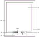
本实施例提供了一种触控显示面板,如图1和图2所示,包括显示区AA和包围显示区AA的边框区BM边框区BM包括触控信号搭接区10。其中,图1所示的触控显示面板为矩形触控显示显示面板(具体可以为手机、平板电脑等),图2所示的触控显示面板为圆形触控显示面板(具体可以为智能手表等可穿戴显示面板)。This embodiment provides a touch display panel. As shown in FIG. 1 and FIG. 2 , it includes a display area AA and a frame area BM surrounding the display area AA. The frame area BM includes a touch
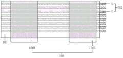
如图3和图4所示,本实施例提供的触控显示面板包括第一基板1和第二基板2。其中,第一基板包括第一衬底101、位于第一衬底101靠近第二基板2一侧的栅极层101、层间绝缘层102和阳极层106;第二基板2包括第二衬底201、位于第二衬底201靠近第一基板1一侧的第一导电层202、第二导电层204和位于第一导电层202和第二导电层204之间的绝缘层203。具体地,第一基板为阵列基板,而第二基板为盖板。As shown in FIG. 3 and FIG. 4 , the touch display panel provided by this embodiment includes a
如图3和图4所示,栅极层102包括位于触控信号搭接区10的多条扇出线L,阳极层106包括位于触控信号搭接区10的多个第一搭接电极1061。As shown in FIG. 3 and FIG. 4 , the
如图3至图5所示,第二基板2包括第二衬底201、第一导电层202、第二导电层204和位于第一导电层202与第二导电层204之间的绝缘层203。其中,第一导电层202包括位于触控信号搭接区10的触控引线2021,第二导电层204包括位于触控信号搭接区10的第二搭接电极2041,第二搭接电极2041与触控引线2021电连接且与第一搭接电极1061适配。As shown in FIGS. 3 to 5 , the
本实施例提供的触控显示面板,通过扇出线的上方的阳极层106制作第一搭接电极1061,能够减小边框的宽度,实现窄边框设计;并且,第二衬底为玻璃盖板时,该方案能够实现in-cell式触控,有利于触控显示面板的轻薄化。In the touch display panel provided in this embodiment, the
需要说明的是,本申请实施例中的触控显示面板中的阵列基板为有机发光显示面板中的阵列基板,虽然图3和图4中并未示出,但实际上,本申请中的触控显示面板还包括有机发光层以及阴极层等,由于有机发光层以及阴极层等不涉及本申请的核心发明点,因此,本申请不对有机发光层以及阴极层等进行展开说明。It should be noted that the array substrate in the touch display panel in the embodiment of the present application is the array substrate in the organic light-emitting display panel. Although it is not shown in FIG. 3 and FIG. The control display panel also includes an organic light-emitting layer and a cathode layer, etc., since the organic light-emitting layer and the cathode layer do not involve the core invention points of the application, therefore, this application does not describe the organic light-emitting layer and the cathode layer.
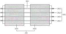
可选地,如图1或图2所示,边框区BM设置有电源负极引线VSS。如图6和图7所示,第一基板1还包括位于层间绝缘层103和阳极层106之间的源漏电极层104,以及位于源漏电极层104和阳极层106之间的平坦化层105。源漏电极层104包括位于触控信号搭接区10的多个屏蔽电极1041,屏蔽电极1041与电源负极引线VSS电连接;第一搭接电极1061在第一衬底101上的正投影覆盖屏蔽电极1041在第一衬底101上的正投影。Optionally, as shown in FIG. 1 or FIG. 2 , the frame region BM is provided with a power supply negative lead VSS. As shown in FIGS. 6 and 7 , the
需要说明的是,为了便于显示第一搭接电极1061和屏蔽电极的关系,图7中并未示出栅极绝缘层和平坦化层。It should be noted that, in order to facilitate the display of the relationship between the
本实施例提供的触控显示面板,通过将位于触控信号搭接区域10的源漏电极层104设计为与电源负极引线VSS连接的屏蔽电极1041,能够防止扇出线上的驱动信号与第一搭接电极1061上的触控信号互相干扰。The touch display panel provided in this embodiment can prevent the driving signal on the fan-out line The touch signals on the
可选地,第一导电层202的材料包括金属钼,第二导电层204的材料包括氧化铟锡(ITO)。Optionally, the material of the first
可选地,如图1所示,边框区BM包括下边框区,下边框区包括外接电路绑定区20和触控信号搭接区10,其中,触控信号搭接区10位于电源负极引线VSS靠近显示区AA的一侧,外接电路绑定区20位于电源负极引线VSS远离显示区AA的一侧。需要说明的是,图2所示的触控显示面板虽然未示出外接电路绑定区,但实际上图2所示的触控显示面板也包括外接电路绑定区。Optionally, as shown in FIG. 1, the frame area BM includes a lower frame area, and the lower frame area includes an external
本实施例通过将触控信号搭接区域10设计在下边框,使得第一搭接电极1061距离同样设置在下边框的外接电路绑定区20较近,有利于减小触控信号的传输电阻。In this embodiment, the touch
可选地,请结合图1、图2和图8,本实施例提供的触控显示面板还包括位于第一基板1与第二基板2之间的封装胶3,各第一搭接电极1061与封装胶3的距离相等。具体地,封装胶3可以涂布在电源负极引线VSS的上方,需要说明的是,电源负极引线VSS可以采用栅极层102来制作。Optionally, referring to FIG. 1 , FIG. 2 and FIG. 8 , the touch display panel provided in this embodiment further includes an
具体地,在矩形显示面板中,第一搭接电极1061可以排布为直线型;在圆形显示面板中,第一搭接电极1061呈弧形阵列排布,只要保证,各第一搭接电极1061与封装胶3的距离相等即可。Specifically, in a rectangular display panel, the first overlapping
本实施例通过使各第一搭接电极1061与封装胶3的距离相等,能够保证各触控信号的传输电阻基板一致,从而提升触控效果,也有利于在制作过程中以及将第一搭接电极1061与第二搭接电极2041对接的过程中,对第一搭接电极1061的位置进行对准,有利于降低第一搭接电极1061的制作难度以及第一搭接电极1061和第二搭接电极2041的对接难度。In this embodiment, by making the distances between the
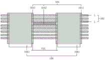
可选地,如图9所示,源漏电极层104还包括位于触控信号搭接区10且连接在相邻屏蔽电极之间的连接线1042,连接线1042在第一衬底101上的正投影与任一扇出线L在第一衬底101上的正投影的距离大于或等于0。也就是连接线1042在第一衬底101上的正投影与任一扇出线1021在第一衬底101上的正投影无交叠,这能够有效避免连接线1042上的信号与扇出线1021上的信号发生干扰。Optionally, as shown in FIG. 9 , the source-
可选地,如图10和图11所示,栅极层102包括第一栅极层1021和第二栅极层1022,第一栅极层1021包括经过触控信号搭接区10的多条第一扇出线L1,第二栅极层1022包括位于触控信号搭接区10的多条第二扇出线L2;第一扇出线L1在第一衬底101上的正投影与第二扇出线L2在第一衬底101上的正投影之间的距离大于或等于0。Optionally, as shown in FIG. 10 and FIG. 11 , the
具体地,为了避免两个栅极层发生短路,阵列基板还包括第一栅极绝缘层GI1和第二栅极绝缘层GI2。Specifically, in order to avoid a short circuit between the two gate layers, the array substrate further includes a first gate insulating layer GI1 and a second gate insulating layer GI2 .
进一步地,在与第一扇出线L1的延伸方向垂直的方向上,第一扇出线L1和第二扇出线L2交替排布。如此设置有利于提高扇出线的布线密度,有利于边框的窄化。Further, in a direction perpendicular to the extending direction of the first fan-out lines L1, the first fan-out lines L1 and the second fan-out lines L2 are alternately arranged. Such setting is beneficial to increase the wiring density of the fan-out lines, and is beneficial to the narrowing of the frame.
本实施例通过将扇出线L设置在第一栅极层1021和第二栅极层1022,并使第一扇出线L1在第一衬底101上的正投影与第二扇出线L2在第一衬底101上的正投影之间的距离大于或等于0,能够防止第一扇出线L1和第二扇出线L2上的信号彼此干扰。In this embodiment, the fan-out line L is arranged on the
如图12和图13所示,外接电路绑定区20包括触控信号绑定结构P,源漏电极层104还包括触控信号转接线1043,触控信号转接线1043的一端与第一搭接电极1061电连接,触控信号转接线1043的另一端与触控信号绑定结构P连接;触控信号转接线1043与屏蔽电极1041之间具有缝隙d,缝隙d的宽度大于触控信号转接线1043与屏蔽电极1041能够互相干扰的距离。As shown in FIG. 12 and FIG. 13 , the external
具体地,如图12所示,转接线1043可以通过过孔与第一栅极层1021中设计的走线与触控信号绑定结构P连接,或者转接线1043通过过孔与第二栅极层1022中设计的走线与触控信号绑定结构P连接。当然,转接线1043可以通过其他方式与触控信号绑定结构P连接,本申请对此不做具体限制,在实际应用中,可以根据触控信号绑定结构P所在的膜层对转接线1043与触控信号绑定结构P连接的具体方式进行选择。Specifically, as shown in FIG. 12 , the
需要说明的是,边框区的宽度能够满足缝隙d的宽度要求,也就是缝隙d的宽度并不会增加边框区的宽度。It should be noted that the width of the frame area can meet the width requirement of the gap d, that is, the width of the gap d will not increase the width of the frame area.
本实施例通过在源漏电极层104制作转接线1043,能够实现触控信号在搭接处与触控信号绑定结构之间的传输;而触控信号转接线1043与屏蔽电极1041之间的距离设置为大于触控信号转接线1043与屏蔽电极1041能够互相干扰的距离,能够避免两者之间发生干扰。In this embodiment, by fabricating the
可选地,如图13所示,平坦化层105包括第一平坦化层1051和第二平坦化层1052,第一平坦化层1051覆盖源漏电极层104且填充在屏蔽电极1041与触控信号转接线1043之间的缝隙d,第二平坦化层1052覆盖第一平坦化层1051。在本实施例中,第一平坦化层1051在起到绝缘以及平坦作用的同时,能够进一步防止屏蔽电极1041与触控信号转接线1043之间发生干扰;采用两层平坦化层能够更好地防止屏蔽电极1041上的信号与触控信号发生干扰。Optionally, as shown in FIG. 13 , the
如图14所示,可选地,第一基板1还包括隔垫物PS,隔垫物PS包括位于显示区AA的第一隔垫物PS1和位于边框区BM的第二隔垫物PS2,第一隔垫物PS1的排布密度大于第二隔垫物PS2的排布密度。As shown in FIG. 14 , optionally, the
具体地,第二隔垫物PS2设置在显示区AA与封框胶3之间。Specifically, the second spacer PS2 is disposed between the display area AA and the
本实施例通过设置隔垫物PS能够保持两个基板之间的距离,以避免两个基板互相挤压而影响电视效果,而设置在边框区BM的第二隔垫物PS2还能够分担在封装胶3烧结后边框区BM的压力,防止压力集中在触控信号搭接区,这能够改善压力集中在局部区域所导致的牛顿环的显示问题。In this embodiment, the distance between the two substrates can be maintained by setting the spacer PS, so as to prevent the two substrates from being pressed against each other and affect the TV effect, and the second spacer PS2 arranged in the frame area BM can also share the burden of the package. After the
“牛顿环”是又称“牛顿圈”,在光学上,牛顿环是一个薄膜干涉现象,其干涉图样是一些明暗相间的同心圆环。本申请中,“牛顿环”是指显示画面呈现环形的明暗相间的显示问题。"Newton's ring" is also known as "Newton's ring". In optics, Newton's ring is a thin film interference phenomenon, and its interference pattern is some concentric rings with alternating light and dark. In the present application, "Newton's ring" refers to a display problem in which the display screen presents a ring shape with alternating light and dark.
如图14和图15所示,第二隔垫物PS2可以由位于边框区BM的第一平坦化层1051和第二平坦化层1052形成,还可以仅由第一平坦化层1051或第二平坦化层1052形成,当然,还可以与显示区AA内的第一隔垫物PS1采用同一膜层同时形成。As shown in FIG. 14 and FIG. 15 , the second spacer PS2 can be formed by the
基于同一发明构思,本实施例提供了一种触控显示面板,该触控显示面板包括上述实施例中的触控显示面板。本实施例提供的触控显示面板能够实现上述实施例中各触控显示面板的有益效果,在此不再赘述。Based on the same inventive concept, this embodiment provides a touch display panel, which includes the touch display panel in the above embodiments. The touch display panel provided in this embodiment can realize the beneficial effects of the touch display panels in the above embodiments, and details will not be repeated here.
进一步地,该触控显示面板为可穿戴触控显示面板。具体地,可穿戴触控显示面板为智能手表、智能手环等。Further, the touch display panel is a wearable touch display panel. Specifically, the wearable touch display panel is a smart watch, a smart bracelet, and the like.
应用本申请实施例,至少能够实现如下有益效果:By applying the embodiments of the present application, at least the following beneficial effects can be achieved:
本实施例提供的触控显示面板和触控显示装置,通过在位于扇出线的上方的阳极层制作第一搭接电极,能够减小边框的宽度,实现窄边框设计;同时,通过将位于触控信号搭接区域的源漏电极层设计为与电源负极引线连接的屏蔽电极,能够防止扇出线上的驱动信号与第一搭接电极上的触控信号互相干扰;并且该方案中的第二基板为盖板,因此该方案能够实现in-cell式触控,有利于触控显示面板的轻薄化。The touch display panel and the touch display device provided in this embodiment can reduce the width of the frame by making the first bonding electrode on the anode layer above the fan-out line, and realize a narrow frame design; The source-drain electrode layer in the overlapping area of the control signal is designed as a shielding electrode connected to the negative lead of the power supply, which can prevent the drive signal on the fan-out line from interfering with the touch signal on the first overlapping electrode; and the second The substrate is a cover plate, so this solution can realize in-cell touch, which is conducive to thinning and thinning the touch display panel.
本技术领域技术人员可以理解,本申请中已经讨论过的各种操作、方法、流程中的步骤、措施、方案可以被交替、更改、组合或删除。进一步地,具有本申请中已经讨论过的各种操作、方法、流程中的其他步骤、措施、方案也可以被交替、更改、重排、分解、组合或删除。进一步地,现有技术中的具有与本申请中公开的各种操作、方法、流程中的步骤、措施、方案也可以被交替、更改、重排、分解、组合或删除。Those skilled in the art can understand that the various operations, methods, and steps, measures, and schemes in the processes that have been discussed in this application can be replaced, changed, combined, or deleted. Furthermore, the various operations, methods, and other steps, measures, and schemes in the processes that have been discussed in this application may also be replaced, changed, rearranged, decomposed, combined, or deleted. Further, steps, measures, and schemes in the prior art that have operations, methods, and processes disclosed in the present application may also be alternated, changed, rearranged, decomposed, combined, or deleted.
在本申请的描述中,需要理解的是,术语“中心”、“上”、“下”、“前”、“后”、“左”、“右”、“竖直”、“水平”、“顶”、“底”、“内”、“外”等指示的方位或位置关系为基于附图所示的方位或位置关系,仅是为了便于描述本申请和简化描述,而不是指示或暗示所指的装置或元件必须具有特定的方位、以特定的方位构造和操作,因此不能理解为对本申请的限制。In the description of this application, it is to be understood that the terms "center", "upper", "lower", "front", "rear", "left", "right", "vertical", "horizontal", The orientations or positional relationships indicated by "top", "bottom", "inner", "outer", etc. are based on the orientations or positional relationships shown in the drawings, and are only for the convenience of describing the application and simplifying the description, rather than indicating or implying References to devices or elements must have a particular orientation, be constructed, and operate in a particular orientation and therefore should not be construed as limiting the application.
术语“第一”、“第二”仅用于描述目的,而不能理解为指示或暗示相对重要性或者隐含指明所指示的技术特征的数量。由此,限定有“第一”、“第二”的特征可以明示或者隐含地包括一个或者更多个该特征。在本申请的描述中,除非另有说明,“多个”的含义是两个或两个以上。The terms "first" and "second" are used for descriptive purposes only, and cannot be interpreted as indicating or implying relative importance or implicitly specifying the quantity of indicated technical features. Thus, a feature defined as "first" and "second" may explicitly or implicitly include one or more of these features. In the description of the present application, unless otherwise specified, "plurality" means two or more.
在本申请的描述中,需要说明的是,除非另有明确的规定和限定,术语“安装”、“相连”、“连接”应做广义理解,例如,可以是固定连接,也可以是可拆卸连接,或一体地连接;可以是直接相连,也可以通过中间媒介间接相连,可以是两个元件内部的连通。对于本领域的普通技术人员而言,可以具体情况理解上述术语在本申请中的具体含义。In the description of this application, it should be noted that unless otherwise specified and limited, the terms "installation", "connection", and "connection" should be understood in a broad sense, for example, it can be a fixed connection or a detachable connection. Connected, or integrally connected; it can be directly connected, or indirectly connected through an intermediary, and it can be the internal communication of two elements. Those of ordinary skill in the art can understand the specific meanings of the above terms in this application in specific situations.
在本说明书的描述中,具体特征、结构、材料或者特点可以在任何的一个或多个实施例或示例中以合适的方式结合。In the description of this specification, specific features, structures, materials or characteristics may be combined in any one or more embodiments or examples in an appropriate manner.
应该理解的是,虽然附图的流程图中的各个步骤按照箭头的指示依次显示,但是这些步骤并不是必然按照箭头指示的顺序依次执行。除非本文中有明确的说明,这些步骤的执行并没有严格的顺序限制,其可以以其他的顺序执行。而且,附图的流程图中的至少一部分步骤可以包括多个子步骤或者多个阶段,这些子步骤或者阶段并不必然是在同一时刻执行完成,而是可以在不同的时刻执行,其执行顺序也不必然是依次进行,而是可以与其他步骤或者其他步骤的子步骤或者阶段的至少一部分轮流或者交替地执行。It should be understood that although the various steps in the flow chart of the accompanying drawings are displayed sequentially according to the arrows, these steps are not necessarily executed sequentially in the order indicated by the arrows. Unless otherwise specified herein, there is no strict order restriction on the execution of these steps, and they can be executed in other orders. Moreover, at least some of the steps in the flowcharts of the accompanying drawings may include multiple sub-steps or multiple stages, and these sub-steps or stages may not necessarily be executed at the same time, but may be executed at different times, and the order of execution is also It is not necessarily performed sequentially, but may be performed alternately or alternately with at least a part of other steps or sub-steps or stages of other steps.
以上所述仅是本申请的部分实施方式,应当指出,对于本技术领域的普通技术人员来说,在不脱离本申请原理的前提下,还可以做出若干改进和润饰,这些改进和润饰也应视为本申请的保护范围。The above description is only part of the implementation of the present application, and it should be pointed out that for those of ordinary skill in the art, without departing from the principle of the present application, some improvements and modifications can also be made, and these improvements and modifications are also It should be regarded as the protection scope of this application.
Claims (11)
Priority Applications (1)
| Application Number | Priority Date | Filing Date | Title |
|---|---|---|---|
| CN201911060674.XACN110825265B (en) | 2019-11-01 | 2019-11-01 | Touch display panel and touch display device |
Applications Claiming Priority (1)
| Application Number | Priority Date | Filing Date | Title |
|---|---|---|---|
| CN201911060674.XACN110825265B (en) | 2019-11-01 | 2019-11-01 | Touch display panel and touch display device |
Publications (2)
| Publication Number | Publication Date |
|---|---|
| CN110825265A CN110825265A (en) | 2020-02-21 |
| CN110825265Btrue CN110825265B (en) | 2023-05-12 |
Family
ID=69552014
Family Applications (1)
| Application Number | Title | Priority Date | Filing Date |
|---|---|---|---|
| CN201911060674.XAActiveCN110825265B (en) | 2019-11-01 | 2019-11-01 | Touch display panel and touch display device |
Country Status (1)
| Country | Link |
|---|---|
| CN (1) | CN110825265B (en) |
Families Citing this family (5)
| Publication number | Priority date | Publication date | Assignee | Title |
|---|---|---|---|---|
| WO2021184309A1 (en)* | 2020-03-19 | 2021-09-23 | 京东方科技集团股份有限公司 | Touch sensor and display device |
| CN111857403A (en)* | 2020-04-24 | 2020-10-30 | 苏州绘格光电科技有限公司 | Touch screen and preparation method thereof |
| CN112416168A (en)* | 2020-11-18 | 2021-02-26 | 云谷(固安)科技有限公司 | Display panel and display device |
| CN113257876B (en)* | 2021-05-12 | 2022-09-23 | 昆山工研院新型平板显示技术中心有限公司 | Display panel and display device |
| CN113407058A (en)* | 2021-06-23 | 2021-09-17 | 昆山国显光电有限公司 | Touch control display panel |
Citations (4)
| Publication number | Priority date | Publication date | Assignee | Title |
|---|---|---|---|---|
| WO2014036754A1 (en)* | 2012-09-07 | 2014-03-13 | 深圳市华星光电技术有限公司 | Fanout wiring design in tft-lcd narrow bezel design |
| CN207557624U (en)* | 2017-08-22 | 2018-06-29 | 京东方科技集团股份有限公司 | A kind of array substrate, display panel and display device |
| CN108550617A (en)* | 2018-06-22 | 2018-09-18 | 武汉天马微电子有限公司 | Display panel and display device |
| CN109917962A (en)* | 2019-03-05 | 2019-06-21 | 业成科技(成都)有限公司 | Touch panel |
- 2019
- 2019-11-01CNCN201911060674.XApatent/CN110825265B/enactiveActive
Patent Citations (4)
| Publication number | Priority date | Publication date | Assignee | Title |
|---|---|---|---|---|
| WO2014036754A1 (en)* | 2012-09-07 | 2014-03-13 | 深圳市华星光电技术有限公司 | Fanout wiring design in tft-lcd narrow bezel design |
| CN207557624U (en)* | 2017-08-22 | 2018-06-29 | 京东方科技集团股份有限公司 | A kind of array substrate, display panel and display device |
| CN108550617A (en)* | 2018-06-22 | 2018-09-18 | 武汉天马微电子有限公司 | Display panel and display device |
| CN109917962A (en)* | 2019-03-05 | 2019-06-21 | 业成科技(成都)有限公司 | Touch panel |
Also Published As
| Publication number | Publication date |
|---|---|
| CN110825265A (en) | 2020-02-21 |
Similar Documents
| Publication | Publication Date | Title |
|---|---|---|
| CN110825265B (en) | Touch display panel and touch display device | |
| CN107193422B (en) | Array substrate, display panel and display device | |
| CN110308822B (en) | Touch display panel and manufacturing method thereof | |
| CN114935983A (en) | A display panel and display device | |
| CN104617106A (en) | Array substrate and display device | |
| WO2020237919A1 (en) | Organic light-emitting diode display apparatus and manufacturing method therefor | |
| CN103984164B (en) | Liquid crystal display device | |
| JP2012530307A (en) | Electromagnetic induction type liquid crystal panel, manufacturing method thereof, and liquid crystal display device | |
| CN104598074A (en) | Touch panel, touch display device and manufacture method of touch panel | |
| CN111580695B (en) | Display panel, manufacturing method thereof and display device | |
| WO2019000912A1 (en) | Display panel and manufacturing method therefor, and display apparatus | |
| JPWO2012144450A1 (en) | Display device | |
| CN111625119B (en) | Touch screen and display device | |
| CN112310183B (en) | Display substrate and preparation method thereof, display device | |
| US11502159B2 (en) | Touch display panel and display device | |
| CN210271564U (en) | Display substrate and display device | |
| CN111708237B (en) | Array substrate, display panel and display device | |
| CN108877543A (en) | A kind of display panel and preparation method thereof, mobile terminal | |
| TWI650701B (en) | Line layout device suitable for narrow frame touch panel | |
| WO2022022151A1 (en) | Display panel and display device | |
| CN107422547A (en) | A kind of display panel and display device | |
| US20170097708A1 (en) | Touch screen, method for manufacturing the same, and display device | |
| CN104571696A (en) | Touch display panel and touch display device | |
| CN103293748B (en) | CF substrate with touch function and touch panel | |
| CN104951121B (en) | Touch display screen and preparation method thereof and display device |
Legal Events
| Date | Code | Title | Description |
|---|---|---|---|
| PB01 | Publication | ||
| PB01 | Publication | ||
| SE01 | Entry into force of request for substantive examination | ||
| SE01 | Entry into force of request for substantive examination | ||
| GR01 | Patent grant | ||
| GR01 | Patent grant |