CN110809705A - Proximity sensor and method of operating the same - Google Patents
Proximity sensor and method of operating the sameDownload PDFInfo
- Publication number
- CN110809705A CN110809705ACN201880040115.XACN201880040115ACN110809705ACN 110809705 ACN110809705 ACN 110809705ACN 201880040115 ACN201880040115 ACN 201880040115ACN 110809705 ACN110809705 ACN 110809705A
- Authority
- CN
- China
- Prior art keywords
- field
- light emitting
- optoelectronic device
- photosensitive
- assembly
- Prior art date
- Legal status (The legal status is an assumption and is not a legal conclusion. Google has not performed a legal analysis and makes no representation as to the accuracy of the status listed.)
- Pending
Links
Images


Classifications
- G—PHYSICS
- G01—MEASURING; TESTING
- G01S—RADIO DIRECTION-FINDING; RADIO NAVIGATION; DETERMINING DISTANCE OR VELOCITY BY USE OF RADIO WAVES; LOCATING OR PRESENCE-DETECTING BY USE OF THE REFLECTION OR RERADIATION OF RADIO WAVES; ANALOGOUS ARRANGEMENTS USING OTHER WAVES
- G01S17/00—Systems using the reflection or reradiation of electromagnetic waves other than radio waves, e.g. lidar systems
- G01S17/02—Systems using the reflection of electromagnetic waves other than radio waves
- G01S17/06—Systems determining position data of a target
- G—PHYSICS
- G01—MEASURING; TESTING
- G01C—MEASURING DISTANCES, LEVELS OR BEARINGS; SURVEYING; NAVIGATION; GYROSCOPIC INSTRUMENTS; PHOTOGRAMMETRY OR VIDEOGRAMMETRY
- G01C3/00—Measuring distances in line of sight; Optical rangefinders
- G01C3/02—Details
- G—PHYSICS
- G01—MEASURING; TESTING
- G01B—MEASURING LENGTH, THICKNESS OR SIMILAR LINEAR DIMENSIONS; MEASURING ANGLES; MEASURING AREAS; MEASURING IRREGULARITIES OF SURFACES OR CONTOURS
- G01B11/00—Measuring arrangements characterised by the use of optical techniques
- G01B11/02—Measuring arrangements characterised by the use of optical techniques for measuring length, width or thickness
- G01B11/026—Measuring arrangements characterised by the use of optical techniques for measuring length, width or thickness by measuring distance between sensor and object
- G—PHYSICS
- G01—MEASURING; TESTING
- G01S—RADIO DIRECTION-FINDING; RADIO NAVIGATION; DETERMINING DISTANCE OR VELOCITY BY USE OF RADIO WAVES; LOCATING OR PRESENCE-DETECTING BY USE OF THE REFLECTION OR RERADIATION OF RADIO WAVES; ANALOGOUS ARRANGEMENTS USING OTHER WAVES
- G01S17/00—Systems using the reflection or reradiation of electromagnetic waves other than radio waves, e.g. lidar systems
- G01S17/02—Systems using the reflection of electromagnetic waves other than radio waves
- G01S17/06—Systems determining position data of a target
- G01S17/08—Systems determining position data of a target for measuring distance only
- G01S17/10—Systems determining position data of a target for measuring distance only using transmission of interrupted, pulse-modulated waves
- G—PHYSICS
- G01—MEASURING; TESTING
- G01S—RADIO DIRECTION-FINDING; RADIO NAVIGATION; DETERMINING DISTANCE OR VELOCITY BY USE OF RADIO WAVES; LOCATING OR PRESENCE-DETECTING BY USE OF THE REFLECTION OR RERADIATION OF RADIO WAVES; ANALOGOUS ARRANGEMENTS USING OTHER WAVES
- G01S17/00—Systems using the reflection or reradiation of electromagnetic waves other than radio waves, e.g. lidar systems
- G01S17/02—Systems using the reflection of electromagnetic waves other than radio waves
- G01S17/06—Systems determining position data of a target
- G01S17/46—Indirect determination of position data
- G—PHYSICS
- G06—COMPUTING OR CALCULATING; COUNTING
- G06F—ELECTRIC DIGITAL DATA PROCESSING
- G06F3/00—Input arrangements for transferring data to be processed into a form capable of being handled by the computer; Output arrangements for transferring data from processing unit to output unit, e.g. interface arrangements
- G06F3/01—Input arrangements or combined input and output arrangements for interaction between user and computer
- G06F3/03—Arrangements for converting the position or the displacement of a member into a coded form
- G06F3/041—Digitisers, e.g. for touch screens or touch pads, characterised by the transducing means
- G06F3/042—Digitisers, e.g. for touch screens or touch pads, characterised by the transducing means by opto-electronic means
- G06F3/0421—Digitisers, e.g. for touch screens or touch pads, characterised by the transducing means by opto-electronic means by interrupting or reflecting a light beam, e.g. optical touch-screen
- H—ELECTRICITY
- H03—ELECTRONIC CIRCUITRY
- H03K—PULSE TECHNIQUE
- H03K17/00—Electronic switching or gating, i.e. not by contact-making and –breaking
- H03K17/94—Electronic switching or gating, i.e. not by contact-making and –breaking characterised by the way in which the control signals are generated
- H03K17/96—Touch switches
- H03K17/9627—Optical touch switches
- H03K17/9631—Optical touch switches using a light source as part of the switch
Landscapes
- Physics & Mathematics (AREA)
- Engineering & Computer Science (AREA)
- Electromagnetism (AREA)
- General Physics & Mathematics (AREA)
- Radar, Positioning & Navigation (AREA)
- Remote Sensing (AREA)
- Computer Networks & Wireless Communication (AREA)
- Theoretical Computer Science (AREA)
- General Engineering & Computer Science (AREA)
- Human Computer Interaction (AREA)
- Length Measuring Devices By Optical Means (AREA)
- Investigating Or Analysing Materials By Optical Means (AREA)
- Light Receiving Elements (AREA)
- Photovoltaic Devices (AREA)
- Hybrid Cells (AREA)
- Optical Radar Systems And Details Thereof (AREA)
Abstract
Translated fromChinese
Description
Translated fromChinese背景技术Background technique
光电接近传感器通常被配置为测量近距离的物体(例如手指、手或耳)的距离。光电接近传感器通过将光引导至物体上并收集从该物体反射的光而操作。通常,所收集的光的强度与物体和光电接近传感器之间的距离相关(例如成比例)。然而,物体具有一定范围的表面反射率。例如,在其中物体是手指、手或耳的情形中,物体的表面反射率可以强烈地取决于皮肤色素沉积。因此,需要可操作为独立于物体表面反射率而测量接近度的光电接近传感器。Photoelectric proximity sensors are typically configured to measure the distance of objects in close proximity, such as fingers, hands, or ears. Photoelectric proximity sensors operate by directing light onto an object and collecting light reflected from the object. Typically, the intensity of the collected light is related (eg, proportional) to the distance between the object and the photoelectric proximity sensor. However, objects have a range of surface reflectivities. For example, in the case where the object is a finger, hand or ear, the surface reflectivity of the object may depend strongly on skin pigmentation. Accordingly, there is a need for an electro-optical proximity sensor operable to measure proximity independent of object surface reflectivity.
发明内容SUMMARY OF THE INVENTION
本公开描述了可操作为大致独立于物体表面反射率而测量接近度的光电装置及其操作方法。本公开中描述的光电装置具有非对称场重叠。非对称场重叠允许大致独立于物体表面反射率的接近度测量。The present disclosure describes optoelectronic devices and methods of operation thereof operable to measure proximity substantially independently of object surface reflectance. The optoelectronic devices described in this disclosure have asymmetric field overlap. Asymmetric field overlap allows proximity measurements that are roughly independent of object surface reflectivity.
在一个方面中,例如,可操作为测量接近度的光电装置包括第一发光组件、第二发光组件和光敏组件。第一发光组件可操作为将光发射至接近光电装置的、位于第一照明场内的位置处的物体上。第一照明场的特征在于第一照明场角度和第一照明场轴线。第二发光组件可操作为将光发射至接近光电装置并位于第二照明场内的位置处的物体上。第二照明场的特征在于第二照明场角度和第二照明场轴线。In one aspect, for example, an optoelectronic device operable to measure proximity includes a first light emitting component, a second light emitting component, and a photosensitive component. The first lighting assembly is operable to emit light onto an object proximate the optoelectronic device at a location within the first illumination field. The first illumination field is characterized by a first illumination field angle and a first illumination field axis. The second light emitting assembly is operable to emit light onto an object at a location proximate the optoelectronic device and within the second illumination field. The second illumination field is characterized by a second illumination field angle and a second illumination field axis.
光敏组件可操作为在视场之上收集光。视场的特征在于视场角度和视场轴线。光敏组件可操作为将由第一发光组件发射的从物体反射的光转换为第一信号。此外,光敏组件可操作为将由第二发光组件发射的从物体反射的光转换为第二信号。光敏组件被布置为与第一发光元件相距第一间距,且光敏组件被布置为与第二发光组件相距第二间距。The photosensitive assembly is operable to collect light over the field of view. The field of view is characterized by a field angle and a field axis. The photosensitive assembly is operable to convert light reflected from the object emitted by the first light emitting assembly into a first signal. Additionally, the photosensitive assembly is operable to convert light reflected from the object emitted by the second light emitting assembly into a second signal. The photosensitive component is arranged at a first spacing from the first light emitting element, and the photosensitive component is arranged at a second distance from the second light emitting component.
在一些情形中,第一发光组件、第二发光组件和/或光敏组件包括光学组件。光学组件可以包括抗反射涂层。In some cases, the first light emitting assembly, the second light emitting assembly, and/or the photosensitive assembly include optical assemblies. The optical assembly may include an anti-reflective coating.
在一些情形中,第一发光组件和第二发光组件包括发光部件。发光部件可以包括发光二极管和/或激光二极管。In some cases, the first light emitting assembly and the second light emitting assembly include light emitting components. The light emitting components may include light emitting diodes and/or laser diodes.
在一些情形中,光敏组件包括光敏部件。光敏部件可以包括光电二极管、电荷耦合器件和/或互补金属氧化物半导体。In some cases, the photosensitive assembly includes a photosensitive component. The photosensitive components may include photodiodes, charge coupled devices, and/or complementary metal oxide semiconductors.
在一些情形中,第一间距大致不等于第二间距,且第一照明场角度大致不等于第二照明场角度。例如,第二间距在第一间距的长度的两倍与十倍之间,且第一照明场角度在第二照明场角度的角度的两倍与十倍之间。In some cases, the first pitch is substantially unequal to the second pitch, and the first illumination field angle is substantially unequal to the second illumination field angle. For example, the second spacing is between two and ten times the length of the first spacing, and the first illumination field angle is between two and ten times the angle of the second illumination field angle.
在一些情形中,非对称场重叠由包括以下中的除了一个之外的全部的配置而获得:In some cases, asymmetric field overlap is obtained by a configuration that includes all but one of the following:


第一照明场轴线大致平行于第二照明场轴线 The first illumination field axis is substantially parallel to the second illumination field axis


在一些实施方式中,第一间距不等于第二间距。在一些情形中,光电装置包括位于第一光敏组件和第二光敏组件中的仅一个上方的光学元件,其中光学元件的存在有利于非对称场重叠。在一些情形中,光电装置包括位于第一光敏组件和第二光敏组件中的每一个上方的相应光学元件,其中位于第一光敏组件上方的光学元件与位于第二光敏组件上方的光学元件的差异有利于非对称场重叠。In some embodiments, the first pitch is not equal to the second pitch. In some cases, the optoelectronic device includes an optical element positioned over only one of the first photosensitive component and the second photosensitive component, wherein the presence of the optical element facilitates asymmetric field overlap. In some cases, the optoelectronic device includes respective optical elements over each of the first photosensitive assembly and the second photosensitive assembly, wherein the difference between the optical element over the first photosensitive assembly and the optical element over the second photosensitive assembly Favorable for asymmetric field overlap.
在一些情形中,在此描述的用于获得非对称重叠的两个或更多方案可以组合使用。In some cases, two or more of the schemes described herein for obtaining asymmetric overlap may be used in combination.
在一些情形中,光电装置包括处理器以及非临时性计算机可读介质,非临时性计算机可读介质包括存储在其上的指令,指令当在处理器上运行时执行包括以下的操作:In some cases, an optoelectronic device includes a processor and a non-transitory computer-readable medium including instructions stored thereon that, when executed on the processor, perform operations including:


对于等于或大于阈值信号比的信号比,使阈值接近值与接近光电装置的物体的位置相关联。 For signal ratios equal to or greater than a threshold signal ratio, a threshold proximity value is associated with the position of an object proximate to the optoelectronic device.
在另一方面中,例如,一种用于操作光电装置的方法包括:In another aspect, for example, a method for operating an optoelectronic device includes:


将由第一发光组件发射、从物体反射并由光敏组件收集的光转换为第一信号 Convert light emitted by the first light-emitting component, reflected from the object, and collected by the photosensitive component into a first signal


将由第二发光组件发射、从物体反射并由光敏组件收集的光转换为第二信号 Convert light emitted by the second light-emitting component, reflected from the object, and collected by the photosensitive component into a second signal


在另一方面中,例如,可操作为测量接近度的光电装置包括发光组件、第一光敏组件和第二光敏组件。发光组件可操作为将光发射至接近光电装置的、位于照明场内的位置处的物体上。照明场的特征在于照明场角度和照明轴线。In another aspect, for example, an optoelectronic device operable to measure proximity includes a light emitting assembly, a first photosensitive assembly, and a second photosensitive assembly. The light emitting assembly is operable to emit light onto an object proximate the optoelectronic device at a location within the illumination field. The illumination field is characterized by the illumination field angle and the illumination axis.
第一光敏组件可操作为在第一视场之上收集光。第一视场的特征在于第一视场角度和第一视场轴线。第一光敏组件可操作为将由发光组件发射的从物体反射的光转换为第一信号。The first photosensitive component is operable to collect light over the first field of view. The first field of view is characterized by a first field of view angle and a first field of view axis. The first photosensitive component is operable to convert light emitted by the light emitting component reflected from the object into a first signal.
第二光敏组件可操作为在第二视场之上收集光。第二视场的特征在于第二视场角度和第二视轴线。第二光敏组件可操作为将由发光组件发射的从物体反射的光转换为第二信号。此外,第一光敏组件被布置为与发光组件相距第一间距,且第二光敏组件被布置为与发光组件相距第二间距。The second photosensitive component is operable to collect light over the second field of view. The second field of view is characterized by a second field of view angle and a second viewing axis. The second photosensitive component is operable to convert light emitted by the light emitting component reflected from the object into a second signal. Furthermore, the first photosensitive component is arranged at a first distance from the light emitting component, and the second photosensitive component is arranged at a second distance from the light emitting component.
在一些情形中,发光组件、第一光敏组件和/或第二光敏组件包括光学组件。光学组件可以包括抗反射涂层。In some cases, the light emitting assembly, the first photosensitive assembly, and/or the second photosensitive assembly include an optical assembly. The optical assembly may include an anti-reflective coating.
在一些情形中,发光组件包括发光部件。发光部件可以包括发光二极管和/或激光二极管。In some cases, the light emitting assembly includes a light emitting component. The light emitting components may include light emitting diodes and/or laser diodes.
在一些情形中,第一光敏组件和第二光敏组件各自包括光敏部件。光敏部件可以包括光电二极管、电荷耦合器件和/或互补金属氧化物半导体。In some cases, the first photosensitive assembly and the second photosensitive assembly each include a photosensitive component. The photosensitive components may include photodiodes, charge coupled devices, and/or complementary metal oxide semiconductors.
在一些情形中,第一间距大致不等于第二间距,且第一视场角度大致不等于第二视场角度。例如,第二间距在第一间距的长度的两倍与十倍之间,且第一视场角度在第二视场角度的角度的两倍与十倍之间。In some cases, the first pitch is not substantially equal to the second pitch, and the first angle of view is not substantially equal to the second angle of view. For example, the second spacing is between two and ten times the length of the first spacing, and the first field of view angle is between two and ten times the angle of the second field of view angle.
在一些情形中,非对称场重叠由包括以下中的除了一个之外的全部的任何配置而获得:In some cases, asymmetric field overlap is obtained by any configuration including all but one of the following:


照明场角度大致等于第一视场角度 The illumination field angle is approximately equal to the first field of view angle


在一些情形中,光电装置可以包括处理器,并且可以包括非临时性计算机可读介质,非临时性计算机可读介质包括存储在其上的指令,指令当在处理器上运行时执行包括以下的操作:In some cases, an optoelectronic device may include a processor, and may include a non-transitory computer-readable medium including instructions stored thereon that, when executed on the processor, execute including the following operate:


对于等于或大于阈值信号比的信号比,使阈值接近值与接近光电装置的物体的位置相关联。 For signal ratios equal to or greater than a threshold signal ratio, a threshold proximity value is associated with the position of an object proximate to the optoelectronic device.
在另一方面中,例如,一种用于操作光电装置的方法包括:In another aspect, for example, a method for operating an optoelectronic device includes:
从发光组件在照明场之上发射光,并发射至接近光电装置且位于照明场内的位置处的物体上 Light is emitted from the light emitting assembly over the illuminated field and onto objects at locations proximate the optoelectronic device and within the illuminated field


利用第二光敏组件收集由发光组件发射并从物体反射的光 The light emitted by the light emitting component and reflected from the object is collected by the second photosensitive component


在一些情形中,该方法进一步包括激活辅助功能的操作,辅助功能实施在主机装置上,光电装置合并在主机装置中。In some cases, the method further includes an act of activating an auxiliary function implemented on the host device in which the optoelectronic device is incorporated.
在一些情形中,辅助功能包括激活合并在主机装置中的显示屏。In some cases, the auxiliary function includes activating a display screen incorporated in the host device.
在一些情形中,辅助功能包括调节传输至合并在主机装置中的部件的电力。In some cases, the auxiliary function includes regulating power delivered to components incorporated in the host device.
在一些情形中,接近光电装置的物体的位置随着时间被收集并作为三维数据存储在非临时性计算机可读介质中。In some cases, the positions of objects proximate the optoelectronic device are collected over time and stored as three-dimensional data in a non-transitory computer-readable medium.
在一些情形中,三维数据包括物体的速度和/或加速度数据。In some cases, the three-dimensional data includes velocity and/or acceleration data of the object.
其他方面、特征和优点将从以下详细说明书、附图和权利要求变得明显。Other aspects, features and advantages will become apparent from the following detailed description, drawings and claims.
附图说明Description of drawings
图1A描绘了具有非对称场重叠的光电装置的示例;示例性装置包括光敏组件和多个发光组件。FIG. 1A depicts an example of an optoelectronic device with asymmetric field overlap; the example device includes a photosensitive component and a plurality of light-emitting components.
图1B描绘了具有非对称场重叠的另一示例性光电装置;示例性装置包括光敏组件和多个发光组件。Figure IB depicts another exemplary optoelectronic device with asymmetric field overlap; the exemplary device includes a photosensitive component and a plurality of light emitting components.
图2描绘了用于操作具有非对称场重叠的光电装置的方法的示例。2 depicts an example of a method for operating an optoelectronic device with asymmetric field overlap.
图3A描绘了具有非对称场重叠的光电装置的示例;示例性装置包括发光组件和多个光敏组件。3A depicts an example of an optoelectronic device with asymmetric field overlap; the example device includes a light emitting component and a plurality of photosensitive components.
图3B描绘了具有非对称场重叠的光电装置的另一示例;示例性装置包括发光组件和多个光敏组件。3B depicts another example of an optoelectronic device with asymmetric field overlap; an example device includes a light emitting component and a plurality of photosensitive components.
图4描绘了用于操作具有非对称场重叠的光电装置的方法的另一示例。4 depicts another example of a method for operating an optoelectronic device with asymmetric field overlap.
图5A图示了其中光敏组件与发光组件等间距的平面图。Figure 5A illustrates a plan view in which the photosensitive components are equidistant from the light emitting components.
图5B图示了其中光敏组件与发光组件不等间距的平面图。Figure 5B illustrates a plan view in which the photosensitive components are unequally spaced from the light emitting components.
图6图示了其中光敏组件的光敏部件在单个半导体芯片中实施的光电装置的示例。Figure 6 illustrates an example of an optoelectronic device in which the photosensitive components of the photosensitive assembly are implemented in a single semiconductor chip.
图7图示了其中用于产生非对称场重叠的多个方案被组合的示例。Figure 7 illustrates an example in which multiple schemes for creating asymmetric field overlap are combined.
具体实施方式Detailed ways
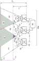
图1A描绘了可操作为独立于物体表面反射率而测量接近度的示例性光电装置100A。光电装置100A包括第一发光组件102、第二发光组件104以及光敏组件106。第一发光组件102可操作为将光108发射至位于第一照明场112内的接近光电装置100A的位置(诸如分别在第一位置111和第二位置113处)的物体110上。第一照明场112由第一照明场角度α和第一照明场轴线114表征。1A depicts an exemplary
第二发光组件104可操作为将光116发射至位于第二照明场118内的接近光电装置100A的位置(诸如分别在第一位置111和第二位置113处)的物体110上。第二照明场118由第二照明场角度β和第二照明场轴线120表征。The second
光敏组件106可操作为在视场122上方收集光。视场122由视场角度γ和视场轴线124表征。当物体110位于第一位置111处时,光109从由第一照明场112和视场122的重叠所描绘的第一区域126中(在二维绘制中)的物体110反射。同样,当物体110位于第一位置111处时,光117从由第二照明场118和视场122的重叠所描绘的区域128中(在二维绘制中)的物体110反射。
类似地,当物体110位于第二位置113处时,光109从由第一照明场112和视场122的重叠所描绘的另一第一区域127中(在二维绘制中)的物体110反射。同样,当物体110位于第二位置113处时,光117从由第二照明场118和视场122的重叠所描绘的另一区域129中(在二维绘制中)的物体110反射。Similarly, when
光敏组件106可操作为将由第一发光组件102发射并从第一位置111处的物体110反射的光109转换为第一信号。同样,光敏组件106进一步可操作为将由第二发光组件104发射并从第一位置111处的物体110反射的光117转换为第二信号。The
此外,光敏组件106被布置为远离第一发光组件102第一间距130,且光敏组件106被布置为远离第二发光组件104第二间距132。Furthermore, the
第一发光组件102、第二发光组件104和光敏组件106各自分别包括光学组件134、136和138,如图1A中所示。每个光学组件可以包括折射或衍射光学元件、微透镜阵列、滤光器或其他光学元件。在其他情形中,第一发光组件102、第二发光组件104和光敏组件106不利用光学组件134、136和138实施。可替换地,第一发光组件102、第二发光组件104和光敏组件106中的任意一个可以分别利用光学组件134、136和138实施。在一些情形中,例如,发光组件102、104可以不利用光学组件134、136实施,但是光敏组件106可以利用光学组件138实施。在一些情形中,任意或所有光学组件134、136和138可以包括抗反射涂层。The first
第一发光组件102和第二发光组件104分别包括第一发光部件140和第二发光部件142,诸如发光二极管、激光二极管、前述的组合或者前述的阵列。第一发光部件140和第二发光部件142不必相同。例如,在一些情形中,第一发光部件140可以是发光二极管,且第二发光部件142可以是激光二极管。第一发光部件140与光学组件134一起可以可操作为从第一发光组件102发射第一特定波长的光108(例如红外光或红光)。同样,第二发光部件142与光学组件136一起可以可操作为从第二发光组件104发射第二特定波长的光116(例如红外光或红光)。The first
光敏组件106可以包括对第一和第二特定波长或波长范围(例如红外光或红光)敏感的光敏部件144,诸如光电二极管、电荷耦合器件、互补金属氧化物半导体、前述的组合或前述的阵列。光敏部件144与光学组件138一起可以可操作为收集从物体110反射的光109和光117。The
本公开中描述的光电装置的特征在于非对称场重叠。如利用示例性光电装置100A所图示的,非对称场重叠允许独立于物体表面反射率的接近度测量。当例如以下时由光电装置100A获得非对称场重叠:The optoelectronic devices described in this disclosure are characterized by asymmetric field overlap. As illustrated with the exemplary
1)第一间距130和第二间距132大致相等;1) The
2)第一照明场轴线114、第二照明场轴线120和视场轴线124均大致平行;2) The first
3)第一照明场角度α和视场角度γ大致相等;以及3) the first illumination field angle α and the field of view angle γ are approximately equal; and
4)第二照明场角度β大致不等于第一照明场角度α或视场角度γ。4) The second illumination field angle β is substantially not equal to the first illumination field angle α or the field of view angle γ.
在一些情形中,第一照明场角度α在第二照明场角度β的两倍和十倍之间。例如,第一照明场角度α可以是60度且第二照明场角度β可以是10度。In some cases, the first illumination field angle α is between two and ten times the second illumination field angle β. For example, the first illumination field angle α may be 60 degrees and the second illumination field angle β may be 10 degrees.
在一些情形中,第一照明场轴线114和第二照明场轴线120大致平行,但是视场轴线124大致不平行。例如,视场轴线124可以相对于第一照明场轴线114或第二照明场轴线120倾斜1度和45度之间或更多。类似地,第一照明场轴线114和第二照明场轴线120可以相对于彼此倾斜1度和45度之间或更多。In some cases, the first
前述配置导致当物体110位于第一位置111处时第一区域126和第二区域128不相等。类似地,当物体110位于第二位置113处时另一第一区域127和另一第二区域129不相等。The foregoing configuration results in the
因为光敏组件106可操作为将从第一区域126和第二区域128发出的光分别转换为第一和第二信号,因此每个信号的幅度将不同,这是因为每个信号名义上与从每个区域反射的光量相关。因此,两个信号之比强烈取决于非对称场重叠,且很大程度独立于物体表面反射率,这是因为在该示例中物体110跨其表面呈现不变的反射率。Because the
图1A图示了第一信号和第二信号之比与物体110的位置之间的关系。对于第一位置111的第一区域126和第二区域128之比以及另一第一区域127和第二区域129之比不同,尽管(如上所述)相对于物体表面反射率不变。因此,第一和第二信号之比可以用于独立于物体表面反射率而确定物体110的位置。FIG. 1A illustrates the relationship between the ratio of the first signal and the second signal and the position of the
光电装置100A可以包括处理器146和非临时性计算机可读介质。可以通过将多个信号比与多个对应位置相关联而校准光电装置。校准的结果可以存储在非临时性计算机可读介质内所包含的标准查找表中,且可以在光电装置100A的使用期间被采用。The
为了利用单个光敏组件102收集第一和第二信号,可以在各自不同时刻转换第一和第二信号。例如,第一发光组件102可以在第一时刻发射光108,其中可以将从物体110反射的光126转换为第一信号,并随后第二发光组件104可以在第二时刻发射光116,其中可以随后将从物体110反射的光128转换为第二信号。In order to collect the first and second signals using a single
图1B描绘了可操作为独立于物体表面反射率而测量接近度的另一示例性光电装置100B,其中光电装置100B中的所有部件(包括部件编号)等同于图1A中所示的部件,除了以下两个例外:间距130和132大致不相等,且第一照明场角度α和第二照明场角度β大致相等。在一些情形中,第二间距可以在第一间距长度的两倍和六倍之间。例如,第一间距可以是1mm且第二间距可以是2mm。因此,如图1A所示产生了非对称场重叠,其中可以使用第一和第二信号之比以独立于物体表面反射率而确定物体110的位置。FIG. 1B depicts another exemplary optoelectronic device 100B operable to measure proximity independent of object surface reflectance, wherein all components (including part numbers) in optoelectronic device 100B are identical to those shown in FIG. 1A , except The following two exceptions are: the
被配置为获得非对称重叠且可操作为独立于物体表面反射率而测量接近度的光电装置的其他实施方式在本公开的范围内。非对称场重叠可以由包括以下中的除了一个之外的全部的配置而获得:Other embodiments of optoelectronic devices configured to achieve asymmetric overlap and operable to measure proximity independently of object surface reflectivity are within the scope of the present disclosure. Asymmetric field overlap can be obtained by configurations that include all but one of the following:


照明场轴线大致平行于第二视场轴线。 The illumination field axis is substantially parallel to the second field of view axis.
在一些实施方式中,第一照明场角度α和第二照明场角度β大致不等,且第一间距和第二间距大致不等。例如,第一照明场角度α在第二照明场角度β的两倍和十倍之间,第二间距可以在第一间距长度的两倍和六倍之间。在一些情形中,第一照明场角度α可以是60度,第二照明场角度β可以是10度,第一间距可以是1mm,以及第二间距可以是2mm。In some embodiments, the first illumination field angle α and the second illumination field angle β are substantially unequal, and the first spacing and the second spacing are substantially unequal. For example, the first illumination field angle α is between two and ten times the second illumination field angle β, and the second spacing may be between two and six times the length of the first spacing. In some cases, the first illumination field angle α may be 60 degrees, the second illumination field angle β may be 10 degrees, the first spacing may be 1 mm, and the second spacing may be 2 mm.
图2描绘了用于操作特征为非对称场重叠的光电装置(诸如图1A和图1B中所示的光电装置)的示例性方法。在202处,从第一发光组件102在第一照明场112之上发射光108并发射至接近光电装置且在第一照明场112内的位置111处的物体110上。2 depicts an exemplary method for operating an optoelectronic device characterized by asymmetric field overlap, such as the optoelectronic device shown in FIGS. 1A and 1B . At 202 , light 108 is emitted from the
在204处,利用光敏组件106收集由第一发光组件102发射并从物体110反射的光109。在206处,将由第一发光组件102发射、从物体110反射并由光敏组件140收集的光转换为第一信号。在208处,从第二发光组件104发射光116至第二照明场118之上并发射至在接近光电装置且在第二照明场118内的位置处的物体110上。在210处,利用光敏组件106收集由第二发光组件104发射并从物体110反射的光117。在212处,将由第二发光组件104发射、从物体110反射并由光敏组件106收集的光117转换为第二信号。At 204 , light 109 emitted by the first
在214处,通过以第二信号归一化第一信号而确定信号比。在216处,从非临时性计算机可读介质调取信号比查找表。信号比查找表包括与多个相应接近值相关联的多个校准信号比。在218处,比较信号比与包括在信号比查找表中的多个校准信号比。在220处,将信号比与多个相应接近值中的至少一个相关联。At 214, a signal ratio is determined by normalizing the first signal with the second signal. At 216, a signal ratio lookup table is retrieved from the non-transitory computer readable medium. The signal ratio lookup table includes a plurality of calibrated signal ratios associated with a plurality of corresponding proximity values. At 218, the signal ratios are compared to a plurality of calibrated signal ratios included in the signal ratio lookup table. At 220, the signal ratio is associated with at least one of a plurality of respective proximity values.
图3A描绘了可操作为独立于物体表面反射率而测量接近度的示例性光电装置300A。光电装置300A包括第一光敏组件302、第二光敏组件304和发光组件306。发光组件306可操作为将光308发射至在照明场312内的接近光电装置300A的位置(诸如分别在第一位置311和第二位置313)处的物体310上。照明场312由照明场角度α和照明场轴线314表征。3A depicts an exemplary
第一光敏组件302可操作为在第一视场316之上收集光。第一视场316由第一视场角度β和第一视场轴线318表征。当物体310位于第一位置311处时,光320从由照明场312和第一视场316的重叠所描绘的第一区域322中(在二维绘制中)的物体310反射。同样,第二光敏组件304可操作为在第二视场324之上收集光。第二视场324由第二视场角度γ和第二视场轴线326表征。当物体310位于第一位置311处时,光328从由照明场312和第二视场324的重叠所描绘的第二区域330中(在二维绘制中)的物体310反射。The first
类似地,当物体310位于第二位置313处时,光320从由照明场312和第一视场316的重叠所描绘的另一第一区域323中(在二维绘制中)的物体310反射。同样,当物体310位于第二位置313处时,光328从由照明场312和第二视场324的重叠所描绘的第二区域331中(在二维绘制中)的物体310反射。Similarly, when
第一光敏组件302可操作为将由发光组件306发射并从第一位置311处的物体310反射的光320转换为第一信号。同样,第二光敏组件304可操作为将由发光组件302发射并从第一位置311处的物体310反射的光328转换为第二信号。The first
此外,第一光敏组件302被布置为远离发光组件306第一间距332,且第二光敏组件304被布置为远离发光组件306第二间距334。如图3A中所示,在一些情形中,两个光敏组件302、304与发光组件306等距(即,间距332、334相等)。也参见图5A。在其他情形中,如以下结合图3B所述的,且如图5B中所示,两个光敏组件302、304与发光组件306间隔不相等(即间距不等)。Furthermore, the first
发光组件306、第一光敏组件302和第二光敏组件304中的每一个可以分别包括光学组件336、338和340,如图3A中所示。每个光学组件可以包括折射或衍射光学元件、微透镜阵列、滤光器或其他光学元件。在其他情形中,发光组件306、第一光敏组件302和第二光敏组件304不利用光学组件336、338和340实施。可替换地,可以分别利用光学组件336、338和340实施发光组件306、第一光敏组件302和第二光敏组件304中的任意一个。在一些情形中,例如,可以不利用光学组件336实施发光组件306,但是可以利用光学组件338、340实施光敏组件302、304。在一些情形中,任意或所有光学组件336、338、340可以包括抗反射涂层。Each of light emitting
发光组件306包括发光部件342,诸如发光二极管、激光二极管、前述的组合或前述的阵列。发光部件342与光学组件340一起可以可操作为从发光组件306发射特定波长的光308(例如红外光或红光)。
第一光敏组件302和第二光敏组件304分别包括对特定波长或波长范围(例如红外光或红光)敏感的第一光敏部件344和第二光敏部件346,诸如光电二极管、电荷耦合器件、互补金属氧化物半导体、前述的组合或前述的阵列。第一光敏部件344和第二光敏部件346不必相同。例如,在一些情形中,第一光敏部件344可以是光电二极管,且第二光敏部件346可以是电荷耦合器件。第一光敏部件344与光学组件336一起可以可操作为收集从物体310反射的光320。同样,第二光敏部件346与光学组件338一起可以可操作为收集光328。The first
如上所述,本公开中描述的光电装置具有非对称场重叠。如利用示例性光电装置300A进一步图示的,非对称场重叠允许独立于物体表面反射率的接近度测量。当例如以下时由光电装置300A获得非对称场重叠:As mentioned above, the optoelectronic devices described in this disclosure have asymmetric field overlap. As further illustrated with the exemplary
1)第一间距332和第二间距334大致相等;1) the
2)第一视场轴线318、第二视场轴线326和照明场轴线314均大致平行;2) the first field of
3)第一视场角度β和照明场角度α大致相等;以及3) the first field of view angle β and the illumination field angle α are approximately equal; and
4)第二视场角度γ大致不等于第一视场角度β或照明场角度α。4) The second field of view angle γ is substantially not equal to the first field of view angle β or the illumination field angle α.
在一些情形中,第一视场角度β在第二视场角度γ的两倍和十倍之间。例如,第一视场角度β可以是60度,且第二照明场角度γ可以是10度。In some cases, the first field of view angle β is between two and ten times the second field of view angle γ. For example, the first field of view angle β may be 60 degrees and the second illumination field angle γ may be 10 degrees.
在一些情形中,第一视场轴线318和第二视场轴线326大致平行,但是照明场轴线314大致不平行。例如,照明场轴线314可以相对于第一视场轴线318或第二视场轴线326倾斜1度和45度之间或更多。类似地,第一视场轴线318和第二视场轴线326可以相对于彼此倾斜1度和45度之间或更多。In some cases, the first field of
前述配置导致当物体310位于第一位置311处时第一区域322和第二区域330不等。类似地,当物体310位于第二位置313处时另一第一区域323和另一第二区域331不等。The foregoing configuration results in the
因为第一光敏组件302可操作为将从第一区域322发出的光320转换为第一信号,且第二光敏组件304可操作为将从第二区域330发出的光328转换为第二信号,因此每个信号的幅度将不同,这是因为每个信号名义上与从每个区域反射的光量相关。因此,两个信号之比强烈取决于非对称场重叠,且很大程度独立于物体表面反射率,这是因为在该示例中物体310跨其表面呈现不变的反射率。Because the first
图3A图示了第一信号和第二信号之比与物体310的位置之间的关系。对于第一位置311的第一区域322和第二区域330之比以及另一第一区域323和第二区域331之比不同,尽管(如上所述)相对于物体表面反射率不变。因此,可以使用第一信号和第二信号之比而独立于物体表面反射率确定物体310的位置。FIG. 3A illustrates the relationship between the ratio of the first signal and the second signal and the position of the
光电装置300A可以包括处理器348和非临时性计算机可读介质。可以通过将多个信号比与多个对应位置相关联而校准光电装置300A。校准的结果可以存储在包含于非临时性计算机可读介质内的标准查找表中,且可以在光电装置300A的使用期间被采用。The
图3B描绘了可操作为独立于物体表面反射率而测量接近度的另一示例性光电装置300B。在图3B中,光电装置300B中的所有部件(包括部件编号)等同于图3A中所示的部件,除了以下两个例外:间距332和330大致不相等(即两个光敏组件302、304与发光组件306的间隔不等),且第二视场角度γ和照明场角度α大致相等。在一些情形中,第二间距可以在第一间距长度的两倍和六倍之间。例如,第一间距可以是1mm且第二间距可以是2mm。因此,如图3A中所描述的,产生了非对称场重叠,其中可以使用第一信号和第二信号之比而独立于物体表面反射率确定物体310的位置。3B depicts another exemplary
被配置为获得非对称重叠且可操作为独立于物体表面反射率而测量接近度的光电装置的其他实施方式在本公开的范围内。非对称场重叠可以由包括以下中的除了一个之外的全部的配置而获得:Other embodiments of optoelectronic devices configured to achieve asymmetric overlap and operable to measure proximity independently of object surface reflectivity are within the scope of the present disclosure. Asymmetric field overlap can be obtained by configurations that include all but one of the following:


在一些实施方式中,第一视场角度β和第二视场角度γ大致不等,且第一间距和第二间距大致不等。例如,第一视场角度β在第二视场角度γ的两倍和十倍之间,第二间距可以在第一间距长度的两倍和六倍之间。在一些情形中,第一视场角度β可以是60度,第二视场角度γ可以是10度,第一间距可以是1mm,且第二间距可以是2mm。In some embodiments, the first field of view angle β and the second field of view angle γ are substantially unequal, and the first spacing and the second spacing are substantially unequal. For example, the first field of view angle β is between two and ten times the second field of view angle γ, and the second spacing may be between two and six times the length of the first spacing. In some cases, the first field of view angle β may be 60 degrees, the second field of view angle γ may be 10 degrees, the first spacing may be 1 mm, and the second spacing may be 2 mm.
图4描绘了用于操作特征在于非对称场重叠的光电装置(诸如图3A和图3B中所绘示例性光电装置)的另一示例性方法。在402处,从发光组件在照明场之上发射光并发射至在接近光电装置且在照明场内的位置处的物体上。4 depicts another exemplary method for operating an optoelectronic device characterized by asymmetric field overlap, such as the exemplary optoelectronic device depicted in FIGS. 3A and 3B. At 402, light is emitted from the light emitting assembly over the illuminated field and onto an object at a location proximate the optoelectronic device and within the illuminated field.
在404处,利用第一光敏组件收集由发光组件发射并从物体反射的光。在406处,将由发光组件发射、从物体反射并由第一光敏组件收集的光转换为第一信号。At 404, light emitted by the light emitting assembly and reflected from the object is collected using the first photosensitive assembly. At 406, light emitted by the light emitting component, reflected from the object, and collected by the first photosensitive component is converted into a first signal.
在408处,利用第二光敏组件收集由发光组件发射并从物体反射的光。在410处,将由发光组件发射、从物体反射并由第二光敏组件收集的光转换为第二信号。At 408, light emitted by the light emitting assembly and reflected from the object is collected using the second photosensitive assembly. At 410, light emitted by the light emitting component, reflected from the object, and collected by the second photosensitive component is converted into a second signal.
在412处,通过以第二信号归一化第一信号而确定信号比。在414处,从非临时性计算机可读介质调取信号比查找表。信号比查找表包括与多个相应接近值相关联的多个校准信号比。在416处,比较信号比与包括在信号比查找表中的多个校准信号比。在418处,将信号比与多个相应接近值中的至少一个相关联。At 412, a signal ratio is determined by normalizing the first signal with the second signal. At 414, a signal ratio lookup table is retrieved from a non-transitory computer readable medium. The signal ratio lookup table includes a plurality of calibrated signal ratios associated with a plurality of corresponding proximity values. At 416, the signal ratios are compared to a plurality of calibrated signal ratios included in the signal ratio look-up table. At 418, the signal ratio is associated with at least one of a plurality of respective proximity values.
在一些情形中,其中光电装置包括发光组件和多个光敏组件的诸如以上所述的实施方式可以提供各种优点。优点可以包括例如较低的功耗。进一步,在一些情形中,光敏组件的光敏部件344、346可以在同一半导体(例如硅)芯片602中实现,如图6的示例中所示。在该情形中,芯片内的两个光敏部件344、346之间的空间可以用于逻辑与电路604,这可以导致光电装置600的较小的总足印(footprint)。进一步,包括发光组件和多个光敏组件的一些实施方式除了可以确定相对距离/接近度之外还可以用于确定实际距离/接近度。In some cases, embodiments such as those described above in which the optoelectronic device includes a light emitting component and a plurality of photosensitive components may provide various advantages. Advantages may include, for example, lower power consumption. Further, in some cases, the
尽管在一些所示实施方式中的发光组件和光敏组件具有相关联的光学元件(例如透镜),但在一些情形中,可以省略光学元件。然而,在一些情形中,可以使用光学元件(诸如透镜)以产生非对称场重叠。在该情形中,在通道之间提供差异。例如,如果实施两个光敏组件(例如图3A或3B),则一个接收通道可以包括透镜,而另一个接收通道不包括。例如,如图7中所示,两个光敏组件302、304与发光组件306的发光部件342等距,但是光敏组件中的仅一个(例如302)包括光学元件(例如透镜)702以产生非对称场重叠。可替换地,两个接收通道均可以包括与另一接收通道中的光学元件(例如透镜)不同的相应光学元件(例如透镜)。当存在透镜时,透镜可以例如经由外壳而相对于光敏组件安装,或者透镜可以直接地模塑至光敏组件的部件上(例如直接模塑至光电二极管顶部上)。Although in some of the illustrated embodiments the light emitting assembly and the photosensitive assembly have associated optical elements (eg, lenses), in some cases the optical elements may be omitted. However, in some cases, optical elements (such as lenses) may be used to create asymmetric field overlap. In this case, differences are provided between the channels. For example, if two photosensitive assemblies are implemented (eg, Figures 3A or 3B), one receiving channel may include a lens while the other receiving channel does not. For example, as shown in Figure 7, two
通常,以上所述用于获得非对称重叠的两个或更多方案可以组合使用。因此,光敏组件的间距差异可以与光学元件(例如透镜)仅在一个光接收通道中的使用(或对于光接收通道使用不同的相应光学元件)组合,以实现非对称重叠。图7中所示的示例,其中两个光敏组件302、304与发光组件306的发光部件342间隔不等(即间距不相等)。不等的间隔引起非对称重叠,但是致力于节省空间,在一些情形中,不相等的间隔可能不足以产生充分的非对称重叠。因此,在一个光敏组件302的光敏部件344之上包括透镜702,这有利于并增强非对称重叠。其他方案(诸如照明场或视场轴线差异)也可以组合,以实现特定量的非对称重叠。In general, two or more of the schemes described above for obtaining asymmetric overlap can be used in combination. Thus, the difference in spacing of the photosensitive components can be combined with the use of optical elements (eg lenses) in only one light receiving channel (or the use of different corresponding optical elements for the light receiving channels) to achieve asymmetrical overlap. The example shown in FIG. 7, wherein the two
一些实施方式包括多个发光组件和多个光敏组件。Some embodiments include multiple light emitting assemblies and multiple photosensitive assemblies.
在一些情形中,上述方法可以包括激活辅助功能,辅助功能实施在主机装置(例如智能电话、平板计算机或膝上型计算机)上,光电装置合并在主机装置中。In some cases, the above-described method may include activating an auxiliary function implemented on a host device (eg, a smartphone, tablet, or laptop) in which the optoelectronic device is incorporated.
在一些情形中,辅助功能包括激活合并在主机装置中的显示屏。例如,在光电装置合并在智能电话中的情形中,用户可以通过将手指定位接近或接触光电装置而激活显示屏。In some cases, the auxiliary function includes activating a display screen incorporated in the host device. For example, in the case of an optoelectronic device incorporated in a smartphone, a user can activate the display screen by positioning a finger near or in contact with the optoelectronic device.
在一些情形中,辅助功能包括调节传输至合并在主机装置中的部件的电力。例如,用户可以通过将手指定位于相对于光电装置的变化位置处,而改变传输至显示屏的电力。在另一示例中,用户可以通过将手指定位于相对于光电装置的变化位置处,而改变传输至光源的电力。In some cases, the auxiliary function includes regulating power delivered to components incorporated in the host device. For example, a user can vary the power delivered to the display by positioning the hand at varying positions relative to the optoelectronic device. In another example, a user can vary the power delivered to the light source by positioning the hand at varying positions relative to the optoelectronic device.
在一些情形中,接近光电装置的物体的位置随着时间被收集并作为三维数据存储在非临时性计算机可读介质中。例如,将物体位置详述为时间的函数的数据可以用于解释姿势。例如,用户可以将手指或手伸到光电装置附近。因此,三维数据可以包括物体的速度和/或加速度数据。In some cases, the positions of objects proximate the optoelectronic device are collected over time and stored as three-dimensional data in a non-transitory computer-readable medium. For example, data detailing object position as a function of time can be used to interpret gestures. For example, a user may place a finger or hand near the optoelectronic device. Thus, the three-dimensional data may include velocity and/or acceleration data of the object.
可以对前述实施方式做出各种修改。上面在不同实施方式中描述的特征可以在同一实施方式中组合。因此,其他实施方式在权利要求的范围内。Various modifications can be made to the foregoing embodiments. Features described above in different embodiments may be combined in the same embodiment. Accordingly, other implementations are within the scope of the following claims.
Claims (35)
Applications Claiming Priority (3)
| Application Number | Priority Date | Filing Date | Title |
|---|---|---|---|
| US201762520029P | 2017-06-15 | 2017-06-15 | |
| US62/520,029 | 2017-06-15 | ||
| PCT/US2018/037514WO2018232105A1 (en) | 2017-06-15 | 2018-06-14 | Proximity sensors and methods for operating the same |
Publications (1)
| Publication Number | Publication Date |
|---|---|
| CN110809705Atrue CN110809705A (en) | 2020-02-18 |
Family
ID=64660761
Family Applications (1)
| Application Number | Title | Priority Date | Filing Date |
|---|---|---|---|
| CN201880040115.XAPendingCN110809705A (en) | 2017-06-15 | 2018-06-14 | Proximity sensor and method of operating the same |
Country Status (5)
| Country | Link |
|---|---|
| US (1) | US11402202B2 (en) |
| EP (1) | EP3638979B1 (en) |
| CN (1) | CN110809705A (en) |
| TW (1) | TWI785062B (en) |
| WO (1) | WO2018232105A1 (en) |
Families Citing this family (3)
| Publication number | Priority date | Publication date | Assignee | Title |
|---|---|---|---|---|
| DE102021132716A1 (en) | 2021-12-10 | 2023-06-15 | OSRAM Opto Semiconductors Gesellschaft mit beschränkter Haftung | RANGE SENSOR AND METHOD OF DETECTING AN OBJECT |
| WO2024189013A1 (en) | 2023-03-15 | 2024-09-19 | Ams-Osram Ag | Sensor and method for operating the sensor |
| WO2025172155A1 (en)* | 2024-02-13 | 2025-08-21 | Ams-Osram Ag | Sensor unit and method for detecting an external object |
Citations (2)
| Publication number | Priority date | Publication date | Assignee | Title |
|---|---|---|---|---|
| CN1276338C (en)* | 2001-11-02 | 2006-09-20 | 内奥诺德股份有限公司 | Display device formed or resting on a substrate |
| US20100245289A1 (en)* | 2009-03-31 | 2010-09-30 | Miroslav Svajda | Apparatus and method for optical proximity sensing and touch input control |
Family Cites Families (7)
| Publication number | Priority date | Publication date | Assignee | Title |
|---|---|---|---|---|
| KR101460813B1 (en) | 2006-09-29 | 2014-11-11 | 오스람 옵토 세미컨덕터스 게엠베하 | Organic light emitting devices and lighting devices |
| US9029756B2 (en)* | 2007-12-05 | 2015-05-12 | PixArt Imaging Incorporation, R.O.C. | Optical displacement detection apparatus and optical displacement detection method |
| US8643628B1 (en)* | 2012-10-14 | 2014-02-04 | Neonode Inc. | Light-based proximity detection system and user interface |
| US8866416B2 (en) | 2011-05-04 | 2014-10-21 | Universal Display Corporation | Illumination source using LEDs and OLEDs |
| US20130321432A1 (en)* | 2012-06-01 | 2013-12-05 | QUALCOMM MEMES Technologies, Inc. | Light guide with embedded fresnel reflectors |
| AU2013317738B2 (en)* | 2012-09-21 | 2015-05-07 | Irobot Corporation | Proximity sensing on mobile robots |
| JP6270808B2 (en)* | 2013-06-27 | 2018-01-31 | パナソニック インテレクチュアル プロパティ コーポレーション オブ アメリカPanasonic Intellectual Property Corporation of America | Motion sensor device having a plurality of light sources |
- 2018
- 2018-06-14EPEP18817554.1Apatent/EP3638979B1/enactiveActive
- 2018-06-14WOPCT/US2018/037514patent/WO2018232105A1/ennot_activeCeased
- 2018-06-14CNCN201880040115.XApatent/CN110809705A/enactivePending
- 2018-06-14USUS16/622,792patent/US11402202B2/enactiveActive
- 2018-06-15TWTW107120866Apatent/TWI785062B/enactive
Patent Citations (2)
| Publication number | Priority date | Publication date | Assignee | Title |
|---|---|---|---|---|
| CN1276338C (en)* | 2001-11-02 | 2006-09-20 | 内奥诺德股份有限公司 | Display device formed or resting on a substrate |
| US20100245289A1 (en)* | 2009-03-31 | 2010-09-30 | Miroslav Svajda | Apparatus and method for optical proximity sensing and touch input control |
Non-Patent Citations (1)
| Title |
|---|
| YONGSIN KIM ET. AL: ""A motion gesture sensor using photodiodes with limited field-of-view"", 《OPTICS EXPRESS》* |
Also Published As
| Publication number | Publication date |
|---|---|
| TW201905493A (en) | 2019-02-01 |
| EP3638979B1 (en) | 2025-08-06 |
| EP3638979A1 (en) | 2020-04-22 |
| EP3638979A4 (en) | 2021-03-24 |
| WO2018232105A1 (en) | 2018-12-20 |
| US20200149884A1 (en) | 2020-05-14 |
| US11402202B2 (en) | 2022-08-02 |
| TWI785062B (en) | 2022-12-01 |
Similar Documents
| Publication | Publication Date | Title |
|---|---|---|
| US20170135617A1 (en) | Optoelectronic modules operable to distinguish between signals indicative of reflections from an object of interest and signals indicative of a spurious reflection | |
| US9970816B2 (en) | Light sensor modules and spectrometers including an optical grating structure | |
| KR20220103962A (en) | Depth measurement via display | |
| US20180073924A1 (en) | Optoelectronic module for spectral and proximity data acquisition | |
| CN106104297A (en) | Optoelectronic module operable to identify false reflections and compensate for errors caused by false reflections | |
| TWI570387B (en) | Image ranging system, light source module and image sensing module | |
| US20080231600A1 (en) | Near-Normal Incidence Optical Mouse Illumination System with Prism | |
| CN110809705A (en) | Proximity sensor and method of operating the same | |
| US9029756B2 (en) | Optical displacement detection apparatus and optical displacement detection method | |
| US20090102793A1 (en) | Optical mouse | |
| CN112513566B (en) | detector for determining the position of at least one object | |
| CN107346411A (en) | Optical sensing module and fingerprint sensing device | |
| CN106289065B (en) | Detection method and optical device applying same | |
| US11239398B2 (en) | Optoelectronic semiconductor component and biometric sensor | |
| TWM552618U (en) | Biometric identification apparatus | |
| TWI360063B (en) | Optical navigation system having a ring pixel arra | |
| CN112074760B (en) | Photovoltaic module and method of operating the same | |
| US9980654B2 (en) | Multi-focus physiologic sensing device for condensing light | |
| US11543499B2 (en) | Hybrid refractive gradient-index optics for time-of-fly sensors | |
| US20180000393A1 (en) | Multiple physiological signals sensing chip and the multiple physiological signals sensing method thereof | |
| TWI651511B (en) | Detection method and optical device using the same | |
| TWI633528B (en) | Display calibration system and display calibration method | |
| TWI639959B (en) | Biometric identification apparatus | |
| TW201602528A (en) | Photometry measurement device | |
| WO2023275242A1 (en) | Measurement head |
Legal Events
| Date | Code | Title | Description |
|---|---|---|---|
| PB01 | Publication | ||
| PB01 | Publication | ||
| SE01 | Entry into force of request for substantive examination | ||
| SE01 | Entry into force of request for substantive examination | ||
| CB02 | Change of applicant information | ||
| CB02 | Change of applicant information | Address after:Hongmao bridge, Singapore Applicant after:AMS sensors Singapore Pte. Ltd. Address before:Hongmao bridge, Singapore Applicant before:Ames sensors Singapore Pte. Ltd. | |
| RJ01 | Rejection of invention patent application after publication | ||
| RJ01 | Rejection of invention patent application after publication | Application publication date:20200218 |